US5103387A - High voltage converter - Google Patents
High voltage converterDownload PDFInfo
- Publication number
- US5103387A US5103387AUS07/648,776US64877691AUS5103387AUS 5103387 AUS5103387 AUS 5103387AUS 64877691 AUS64877691 AUS 64877691AUS 5103387 AUS5103387 AUS 5103387A
- Authority
- US
- United States
- Prior art keywords
- high voltage
- circuit means
- power
- switch
- voltage converter
- Prior art date
- Legal status (The legal status is an assumption and is not a legal conclusion. Google has not performed a legal analysis and makes no representation as to the accuracy of the status listed.)
- Expired - Fee Related
Links
- 238000004804windingMethods0.000claimsabstractdescription17
- 239000003990capacitorSubstances0.000claimsdescription3
- 238000001514detection methodMethods0.000claimsdescription3
- 230000011664signalingEffects0.000description24
- 238000010586diagramMethods0.000description11
- 239000013643reference controlSubstances0.000description9
- 238000007599dischargingMethods0.000description3
- 230000017525heat dissipationEffects0.000description3
- 230000002159abnormal effectEffects0.000description2
- 230000015572biosynthetic processEffects0.000description2
- 238000006243chemical reactionMethods0.000description2
- 230000000737periodic effectEffects0.000description2
- 230000005540biological transmissionEffects0.000description1
- 238000004891communicationMethods0.000description1
- 238000007667floatingMethods0.000description1
- 238000000034methodMethods0.000description1
- 239000013641positive controlSubstances0.000description1
- 238000007789sealingMethods0.000description1
- 230000001052transient effectEffects0.000description1
- 230000007704transitionEffects0.000description1
Images


Classifications
- H—ELECTRICITY
- H04—ELECTRIC COMMUNICATION TECHNIQUE
- H04M—TELEPHONIC COMMUNICATION
- H04M19/00—Current supply arrangements for telephone systems
- H04M19/02—Current supply arrangements for telephone systems providing ringing current or supervisory tones, e.g. dialling tone or busy tone
- H—ELECTRICITY
- H02—GENERATION; CONVERSION OR DISTRIBUTION OF ELECTRIC POWER
- H02M—APPARATUS FOR CONVERSION BETWEEN AC AND AC, BETWEEN AC AND DC, OR BETWEEN DC AND DC, AND FOR USE WITH MAINS OR SIMILAR POWER SUPPLY SYSTEMS; CONVERSION OF DC OR AC INPUT POWER INTO SURGE OUTPUT POWER; CONTROL OR REGULATION THEREOF
- H02M3/00—Conversion of DC power input into DC power output
- H02M3/22—Conversion of DC power input into DC power output with intermediate conversion into AC
- H02M3/24—Conversion of DC power input into DC power output with intermediate conversion into AC by static converters
- H02M3/28—Conversion of DC power input into DC power output with intermediate conversion into AC by static converters using discharge tubes with control electrode or semiconductor devices with control electrode to produce the intermediate AC
- H02M3/325—Conversion of DC power input into DC power output with intermediate conversion into AC by static converters using discharge tubes with control electrode or semiconductor devices with control electrode to produce the intermediate AC using devices of a triode or a transistor type requiring continuous application of a control signal
- H02M3/335—Conversion of DC power input into DC power output with intermediate conversion into AC by static converters using discharge tubes with control electrode or semiconductor devices with control electrode to produce the intermediate AC using devices of a triode or a transistor type requiring continuous application of a control signal using semiconductor devices only
- H02M3/33569—Conversion of DC power input into DC power output with intermediate conversion into AC by static converters using discharge tubes with control electrode or semiconductor devices with control electrode to produce the intermediate AC using devices of a triode or a transistor type requiring continuous application of a control signal using semiconductor devices only having several active switching elements
Definitions
- the present inventionrelates to a high voltage converter for providing a load with an AC power of the desired waveform in which charging and discharging of the power to and from the load is controlled. More specifically, the invention is directed to the high voltage converter used in a system where controlled DC power, AC power and a combination of both are required for its operation.
- the system to which the present invention can be appliedis the telephone system where controlled DC and/or AC voltage higher than a DC source voltage provided in the system is required for certain telephony functions.
- party linesmay require "selective ringing", involving: (a) providing the ringing voltage to one or other side of the line, relative to ground; (b) superimposing either a negative or a positive DC voltage onto the AC ringing voltage; (c) ringing at different frequencies.
- For message waiting signallingit is essential that the voltage be applied and removed slowly, in order to avoid sounding the subscriber's ringers.
- the maximum current delivered to each lineshould be limited for safety reasons not to exceed a few milliamperes.
- U.S. Pat. No. 4,761,812 issued August 1988teaches a constant power telephone line circuit. It comprises a flyback switching power converter having a switching transistor circuit, a transformer having a primary winding coupled to the switching transistor circuit and device for discharging energy stored in the core such that the power output is a constant power pulse.
- U.S. Pat. No. 4,674,119, issued June 16, 1987 (Chea, Jr.)describes a wide band high voltage amplifier for telephony. It also uses a flyback generator with a capacitor storage element coupled across the line and an error signal controls the energy transfer from the flyback converter to the line.
- U.S. Pat. No. 4,056,689, issued Nov. 1, 1977 (Freimanis)describes a communication line interface circuit including a floating current source supplying a constant current substantially independent of loop length. The line interface circuit is provided with circuitry for line supervision and the detection of dial pulse signalling.
- such convertersare useful in the field of motor control of computer tape drives, and of read/write heads in computer disk drives, which are required to have rapid starting, stopping, and reversing characteristics.
- the converterIn telephony, the converter should be able to supply DC power of an adjustable voltage for providing balanced line feed for the idle, addressing and transmission states of the line. It should also be able to supply AC power of a desired waveform at voltages higher than the DC source voltage.
- a voltage higher than a DC sourceis used if, for example, it should happen that the DC source voltage typically from a battery is unusually low.
- a voltage lower than the DC sourcemight be used when the line resistance is less than the normal maximum.
- the convertercan alternatively supply signalling power to one or the other side, or both sides, of the line, when the situation requires voltages higher than or of the opposite polarity from that of the DC source. These situations include ringing, coin telephone signalling and control, and message-waiting signalling.
- the present inventionrelates to a high voltage converter for providing a power to a load by load connection lines from a DC voltage source.
- the convertercomprises a line driver circuit means to be connected to the DC voltage source for providing a line drive output and high voltage circuit means to be connected to the DC voltage source for providing a high voltage output. It further includes connection switch means for selectively connecting the line driver circuit means and the high voltage circuit means to the load connection lines for providing the line drive output, the high voltage output or a combination thereof.
- the high voltage circuit meansin turn comprises a flyback transformer which has a primary winding and two secondary windings.
- the high voltage circuit meansfurther includes a primary transistor switch connected to the primary winding for supplying the pulsed power thereto from the DC voltage source in a controlled pulsing manner and a secondary transistor switch and diode combination connected to each of the two secondary windings for controlling the flow of the power generated therein as the result of the power supplied to the primary winding.
- Each of the secondary transistor switchesis turned on or off in a controlled manner so that a high voltage output of a specific waveform is produced.
- FIG. 1is a schematic block diagram of the high voltage converter according to one embodiment of the invention.
- FIG. 2shows diagrams of voltage-current characteristics of some typical loads
- FIG. 3is a schematic circuit diagram of the high voltage circuit means according to one embodiment of the invention.
- FIG. 4is a block diagram of the power control circuit according to one embodiment of the invention.
- FIG. 5is a schematic circuit diagram of the high voltage circuit means according to another embodiment of the invention.
- FIG. 6is a circuit diagram of the overcurrent detector circuit
- FIG. 7is a circuit diagram of the power switching control circuit according to one embodiment of the invention.
- FIG. 8shows power switching control circuit output signals
- FIG. 9a and 9bare schematic block diagrams showing switch configurations according to two embodiments of the invention.
- FIG. 1shows in a schematic block diagram the high voltage converter system according to one embodiment of the present invention.
- a load 10is supplied with a controlled power by load connection lines which may be four lines in simplex configuration in other embodiments.
- a line driver circuit means 12provides various controlled DC power or AC of a desired waveform, or a combination of both to its output terminals which are connected to a current and voltage sensing network 14 via connection switch network 16 consisting of a plurality of switches S 1 , S 2 , S 3 . . .
- a high voltage circuit means 18produces a high voltage output either in AC or DC or both which is sent to the connection switch network 16.
- connection switch networkBy specifically configuring the connection switch network, the high voltage output can be supplied to the load through any of the load connection lines either directly or by way of the line driver circuit means 12.
- a power control circuit means 20is under control of a program load and command 22 and is responsive to the sensing output of the current and voltage sensing network 14 to generate control signals for the high voltage circuit means 18 and the connection switch network 16.
- a battery or other DC power source 24provides not only the operating power for various circuits and networks but also the power which is supplied to the load directly or the power which is to be converted by the high voltage circuit means before being supplied to the load.
- the connection switch network 16can be constructed from mechanical switches, solid-state switches or a combination of these.
- the power control circuit meansmay include a combination of digital and analog hardware, operated by a digital controller which may be implemented using computer architecture with stored program software.
- a high voltage convertermay involve driving reactive loads in both negative and positive polarities, such that power must at some times be delivered to the load, but at other times must be discharged from the load.
- the converteris able to operate in four distinct modes, or “quadrants", and is able to switch moderately quickly from any mode to any other mode.
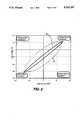
- the four operating quadrantswill here be called active source, passive source, active sink, and passive sink. They are shown on a voltage-current diagram in FIG. 2.
- a graph 30indicates the voltage-current characteristics of a standard load impedance in the telephone system as an example and chosen to be equivalent to 5 ringers in parallel, being driven by a voltage that is controlled to vary sinusoidally with time, superimposed on a DC voltage component.
- a telephone ringerdraws an AC component of current but not a DC component.
- the evident elliptical shape of the voltage-current curveindicates that the load impedance in this example includes a reactive component. Owing to the existence of a DC component of voltage but not of current, the operating characteristic in this example enters three but not all of the quadrants. However, in cases where the load has a higher reactance or there is no DC superimposition, the operation of the high voltage converter could enter into all four quadrants in turn, as shown by a graph 32.
- FIG. 3illustrates schematically the high voltage circuit means according to one embodiment of the invention.
- transistor Q1For operation in the active source and active sink quadrants, transistor Q1 is switched on and off at a periodic high frequency by a pulsing control signal PCD. While Q1 is conducting, energy is transferred from the battery or other DC source to transformer T1. When Q1 turns off, T1 supplies energy to a reservoir capacitor C1 by the known principles of a flyback power converter. T1 is provided with two secondary windings, and correspondingly two rectifying diodes D1, D2.
- the high voltage circuit meansis provided with two "grounding switches" consisting of transistors Q2 and Q3 with associated driver circuits.
- the voltage provided to the load 30may be chosen to be of either polarity. To minimize power losses, the transistor selected to conduct is made to be as fully conducting as is reasonably possible.
- the output poweris controlled by varying the "ON" duty cycle of Q1. Control signals applied to the Q2 and Q3 driver circuits turn Q2 and Q3 on and off in desired manner so that required turns-on/off durations, timings, waveforms of the output, etc. can be controlled.
- the high voltage circuit means of FIG. 3utilizes the same transistors Q2 and Q3 for discharging power from the load in the operation of passive source or passive sink quadrants. In these operations, since no power is required to be taken from the battery, Q1 is held non-conducting. By making selected Q2 or Q3 conduct in a controlled manner, power can be discharged at the rate needed at any time to maintain the desired instantaneous voltage across the load of various impedance values.
- the line driver circuit means 12provides a variety of controlled DC power or normal voice or information carrying tone AC signal power at its output terminals.
- the line driver circuit meanscontains multiple of ICs, e.g. op amps etc., and therefore the terminals VEE and VCC are provided for their operation.
- the terminal VCCis supplied with the regular operating power from the DC power supply 24.
- Various switch configurations of the connection switch means 16can be chosen so that the terminal VEE is supplied with power either from the DC power source or the high voltage circuit means as a need for increased voltage or desired waveforms could arise.
- connection switch meansdetermine the operating modes that can be provided.
- Table 1shows how the switches S1 through S8 shown in FIG. 1 allow various telephony operating modes to be provided.
- LDC and HVCstand for the line driver circuit and the high voltage circuit, e.g. the means shown in FIG. 1 by 12 and 18, respectively. Of course, there are many other possible combinations of these switches which are appropriate for other applications.
- the high voltage circuit meansWhen S1 is closed, the battery negative lead is connected to the negative supply point VEE of the line driver circuit means. In this situation, either S2 should be open, or if it is closed, the high voltage circuit means must be inactive. S1 may be opened, and S2 closed, to supply power to the loop via the high voltage circuit means. The usual reason for doing this is to provide a voltage different from that of the battery.
- the high voltage circuit meansmay be designed so that when inactive, it presents a high impedance at its output terminals. This will be assumed to be the case.
- FIG. 4is a block circuit diagram of the power control circuit means 20 which includes a reference control circuit 40, a summing circuit 42, low-pass filter 43, and a power switching control circuit 44.
- the reference control circuit 40generates a smooth analog reference voltage Vref that is a replica (on a reduced scale) of the loop powering voltage or signalling voltage that is to be generated.
- the summing circuit 42generates a voltage difference between Vref and a fraction k of the output voltage Vout of the high voltage circuit means, which is filtered by the low-pass filter to create an error voltage Verr.
- the low-pass filteris provided to remove high-frequency noise.
- the reference control circuit 40can be made of hard-wired circuit or computer-type architecture, operated by stored program coding.
- the current and voltage sensing network 14produces signals indicative of other conditions of the power supplied to the load, e.g. differential current etc. In telephony, the common mode current can be sensed here also.
- the high voltage circuit meanscan be provided with an overcurrent detector which generates an overcurrent trip signal 50 whose message 52 can be sent to the reference control circuits 40.
- the power switching control circuit 44determines in which quadrant of operation the power converter is required to be at any time, and applies control voltages to the transistor switches Q1, Q2, Q3 of the high voltage circuit means in such a way as to reduce the error voltage.
- Table 2illustrates, in terms of six different operating situations, how the four quadrants can be identified by the sign of Vref and by the sign and magnitude of Verr. They define whether Q1 should be pulsed, and which of Q2 or Q3 should be turned on, and whether the status of Q1 or Q3 should be highly conductive, or conducting in a controlled manner in proportion to the magnitude of the error.
- the pulse duration applied to Q1must never exceed a defined maximum value, in order to allow sufficient time for flyback, when the energy transferred into transformer T1 during the "on" period of Q1 is transferred to the load.
- optional but preferred "hold zones”are defined in Table 2. The purpose of the hold zones is to avoid problems caused by finite turn-off times and finite turn-on times in switches Q2 and Q3.
- the specific function of the reference control circuit in steady conditionsmay be to provide a constant reference voltage. This may not be the case during or following transient changes.
- the reference control circuitmust provide a time-varying reference voltage.
- ISDNIntegrated Services Digital Network
- the reference control circuitmay require the application of time-varying (ramped) "sealing current" power to the loop.
- the reference control circuitprovides a time-varying reference voltage.
- the reference control circuitmay be required to make adjustments to the reference voltage in response to changes in the line currents--either the loop (differential) current, or the longitudinal (common mode) current, or to the current in one or the other of the load connection lines.
- the purpose of such adjustmentsmay include limiting the current in accordance with a defined standard of operation, reducing heat dissipation within the line circuit, reducing potential hazard to personnel, or reducing any risk of damage to the components of high voltage circuit means due to overcurrent caused by abnormal loop conditions, such as ground faults or lightning.
- one of the functions of the reference control circuitwould be to analyze the sensing data in relation to the function being performed, then either re-enable the high voltage circuit means, or leave it disabled.
- FIG. 5shows another embodiment of the high voltage circuit means.
- Transistors Q1, Q2 and Q3are power-switching MOS transistors.
- elements R1, R2, Q4, Q5 and Q6provide level shifting between the control signal levels provided by the power switch control circuit, and levels close to battery negative voltage. Additionally, they are able to drive Q1 on and off at high speeds, as required for efficient power conversion. Owing to level inversion by Q4, the required logical control signal is not PCD as in FIG. 3, but the inverse, here labelled PCDB.
- Q2is driven directly by the control signals from the power switch control circuit. Typically, the levels of these signals would be less than 1 V (off) and up to about 10 V (on), so that Q2 can be a power MOS transistor of a standard type, yet have a low resistance to current flow when fully "on”.
- Q3is required to be able to control conduction at negative voltages.
- Q3is chosen to be of similar type to Q2, (n-channel MOS), and is arranged to control negative voltages by grounding its drain contact instead of the source contact as for Q2.
- the control gate of Q3must follow close to the high negative voltage that can exist on the source contact of Q3.
- Elements R3, R4 and Q7provide level shifting to control the gate voltage of Q3 under all conditions, when driven by control signal PGB, the inverted form of PG.
- high voltages on the control gate of Q3could be avoided by choosing Q3 to be a p-channel MOS, with its source grounded. If, in addition, Q3 were chosen to be normally-on (depletion type) MOS, its gate could be driven directly by positive control signals.
- resistor R5which has low ohmic value (typically about 1 ohm) and a detector circuit 60, which monitors the voltage drop across R5 to provide fast detection of excessive current in either polarity. This could be caused by sudden changes in the line conditions, either being normal conditions (e.g. ringing answer) or abnormal conditions (e.g. line surges).
- the power switch control circuitthen turns off Q1, Q2 and Q3, the high voltage circuit means can be disabled within a very short time, preventing possible damage to the components of the high voltage circuit means.
- FIG. 6is a practical implementation of the detector circuit 60. It consists of R6 and Q8, which respond to one polarity of excessive current, (causing positive voltage input to the detector) and R7 and Q9, which respond to the opposite polarity of current. The result is that an excessive current in either polarity through R5 causes a warning current in one polarity to appear at the detector output point, labelled OC.
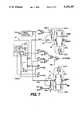
- FIG. 7shows a possible implementation of the power switching control circuit.
- Elements R1 to R3, C1 and A1 within the shaded boundary 70provide the functions of the summing circuit 42 and low-pass filter 43 in FIG. 4, producing the error voltage Verr.
- Elements R4, R5 and A2generate -Verr (inverted error).
- Amplifiers A3 and A4operate as comparators, generating digital signals SR and SE, respectively, defining the sign of the reference and the sign of the error.
- Amplifiers A5 and A6operate as fast comparators, respectively, comparing Verr and -Verr against a periodic voltage ramp Vrmp, and thereby producing pulse-width modulated digital signals PWA and PWB.
- one or other of logical AND gates G1 or G2is enabled to pass signal PCDB.
- G4also receives a logically-unconditional (clock) signal DM, which constrains the pulse width to a chosen maximum value. This ensures that Q1 in the high voltage circuit means is always switched off for a sufficient time to complete the flyback portion of its switching cycle, for every required voltage and load impedance combination.
- gate G5together with switch SW1, resistor network 72 and differential amplifier 74, provide the voltage levels of NG to control the required states of Q2, namely being “off", or “on” with a conduction proportional to Verr, or "on” in a heavily-conducting state.
- gate G6together with switch SW2, resistor network 76 and differential amplifier 78 provide the required levels of PGB, controlling the states of Q3.
- the ramp Vrmpcommences at a voltage that is offset from the comparator reference Vdcref by a small amount. When the error magnitude is smaller than this amount, no pulse is produced at PCDB. This aids in creating the "hold zones" shown in FIG. 5.
- the reference voltage Vdeltalshould be set to a level more negative than Vdcref, so that for small error magnitudes, the NG level is clamped at VDC-.
- the reference voltage Vdelta2should be set to a level that is more positive than Vdcref, so that for small error magnitudes the PGB level is clamped at VDC+.
- This clamping of NG and PGB at small error magnitude, together with the offset in the ramp voltage as mentioned above,may incidentally cause the formation of hold zones in the passive quadrants.
- the purpose of the offsetsis to ensure that for sufficiently small errors, the discharge of energy from the load can be effectively prevented.
- FIG. 8further illustrates the formation of PWA and PWB from both smaller and larger examples of the error voltage, respectively labelled Verr(1) and Verr(2) and the form of the control signals NG, PCDB and PGB, for the large and small error examples Verr(1) and Verr(2).
- FIGS. 9a and 9billustrate possible implementations of the connection switches network.
- S1is a solid-state switch, providing the same functions as S1 in FIG. 1.
- solid-state switchesare convenient when the closed-circuit resistance is not required to be very low.
- K1 and K2are metallic relays.
- FIG. 9aa symmetrical configuration of K1 and K2 provides signalling functions 1, 2, 3, 4, 5, and 7 as listed in Table 1, but excludes normal coin signalling, listed as number 6, because it is not possible to open-circuit the Ring lead while the high voltage circuit means is active.
- relays K1 and K2are connected in an offset manner, that provides the functions 1, 2, 3, 4, 5, and 6, but not the alternate form of coin signalling, listed as number 7.
- Table 3shows the available operating modes and corresponding switch and relay states for both configurations.
Landscapes
- Engineering & Computer Science (AREA)
- Power Engineering (AREA)
- Signal Processing (AREA)
- Dc-Dc Converters (AREA)
- Devices For Supply Of Signal Current (AREA)
Abstract
Description
TABLE 1 __________________________________________________________________________ HVC # S1 S2 S3 S4 S5 S6 S7 S8 STATUS TELEPHONY APPLICATION __________________________________________________________________________1 C X C C -- -- -- -- inactive Loop Idle or DC feed (LDC on Tip, Ring) 2 -- C C C -- -- -- -- active Loop Idle or DC feed (LDC on Tip, Ring) 3 C -- -- C X -- -- -- inactive Ground Start (Tip open, LDC on Ring) 4 C -- -- C C -- -- -- active Signalling on Tip (HVC on Tip, LDC on Ring) 5 X -- -- -- C -- -- -- active Coin signalling on Tip (HVC on Tip, Ring open) 6 C -- C -- -- C -- -- active Signalling on Ring (HVC on Ring, LDC on Tip) 7 X -- -- -- C C -- -- active Simplex Coin signalling (HVC on both Tip & Ring) 8 X -- -- -- C -- -- C active Signalling on Tip (HVC on Tip, Gnd on Ring) 9 X -- -- -- -- C C -- active Signalling on Ring (HVC on Ring, Gnd on Tip) __________________________________________________________________________ Definition of symbols: -- = open C = closed X = status unimportant (a "don't care" state).
TABLE 2 __________________________________________________________________________Power Converter Situations (Inset) Sign of Sign (Magnitude) Functions of Power Switching Control Circuit No. Reference of Error # Quadrant NG (Q2) PCD (Q1) PG (Q3) __________________________________________________________________________1 Negative Negative Passive OFF OFFVariable Source 2 Negative Positive (small) Hold Highly OFF OFF 3 Negative Positive Active Conducting Var. pulse Sink 4 Positive Negative Active OFF Var. pulse Highly Source Conducting 5 Positive Negative (small) Hold OFF 6 Positive Positive Passive Variable OFF OFF Sink __________________________________________________________________________
TABLE 3 __________________________________________________________________________FIG. 9a FIG. 9b # S1 K1 K2 HVC S1 K1 K2 HVC TELEPHONY APPLICATION __________________________________________________________________________1 C -- -- inactive C -- -- inactive Loop Idle or DC feed (LDC on Tip, Ring) 2 -- -- -- active -- -- -- active Loop Idle or DC feed (LDC on Tip, Ring) 3 C E -- inactive C E -- inactive Ground Start (Tip open, LDC on Ring) 4 C E -- active C E -- active Signalling on Tip (HVC on Tip, LDC on Ring) 5 Not available C E E active Coin signalling on Tip (HVC on Tip, Ring open) 6 C -- E active C -- E active Signalling on Ring (HVC on Ring, LDC on Tip) 7 C E E active Not available Simplex Coin signalling (HVC on both Tip & Ring) __________________________________________________________________________ Definition of symbols: -- = switch S1 open, or relay Kn not energized C = switch S1 closed E = relay Kn energized
Claims (11)
Priority Applications (5)
| Application Number | Priority Date | Filing Date | Title |
|---|---|---|---|
| US07/648,776US5103387A (en) | 1991-01-31 | 1991-01-31 | High voltage converter |
| CA002059055ACA2059055C (en) | 1991-01-31 | 1992-01-08 | High voltage converter |
| US07/862,478US5323461A (en) | 1991-01-31 | 1992-04-02 | Telephone line interface circuit with voltage switching |
| US08/200,081US5666406A (en) | 1991-01-31 | 1994-02-10 | Hazard prevention for telephone line interface circuits |
| US08/426,438US5511118A (en) | 1991-01-31 | 1995-04-21 | Method of providing d.c. feed to a telephone line |
Applications Claiming Priority (1)
| Application Number | Priority Date | Filing Date | Title |
|---|---|---|---|
| US07/648,776US5103387A (en) | 1991-01-31 | 1991-01-31 | High voltage converter |
Related Child Applications (1)
| Application Number | Title | Priority Date | Filing Date |
|---|---|---|---|
| US07/862,478Continuation-In-PartUS5323461A (en) | 1991-01-31 | 1992-04-02 | Telephone line interface circuit with voltage switching |
Publications (1)
| Publication Number | Publication Date |
|---|---|
| US5103387Atrue US5103387A (en) | 1992-04-07 |
Family
ID=24602191
Family Applications (2)
| Application Number | Title | Priority Date | Filing Date |
|---|---|---|---|
| US07/648,776Expired - Fee RelatedUS5103387A (en) | 1991-01-31 | 1991-01-31 | High voltage converter |
| US07/862,478Expired - LifetimeUS5323461A (en) | 1991-01-31 | 1992-04-02 | Telephone line interface circuit with voltage switching |
Family Applications After (1)
| Application Number | Title | Priority Date | Filing Date |
|---|---|---|---|
| US07/862,478Expired - LifetimeUS5323461A (en) | 1991-01-31 | 1992-04-02 | Telephone line interface circuit with voltage switching |
Country Status (2)
| Country | Link |
|---|---|
| US (2) | US5103387A (en) |
| CA (1) | CA2059055C (en) |
Cited By (13)
| Publication number | Priority date | Publication date | Assignee | Title |
|---|---|---|---|---|
| US5321596A (en)* | 1991-03-25 | 1994-06-14 | Raynet Corporation | DC/DC/AC power supply for a subscriber interphase unit |
| US5511118A (en)* | 1991-01-31 | 1996-04-23 | Northern Telecom Limited | Method of providing d.c. feed to a telephone line |
| US5539820A (en)* | 1994-10-06 | 1996-07-23 | Northern Telecom Limited | Protection of active telephone line interface circuits |
| EP0695980A4 (en)* | 1994-02-23 | 1996-07-24 | New Japan Radio Corp Ltd | Ac driving device |
| US5636274A (en)* | 1995-01-13 | 1997-06-03 | Harris Corp. | Switch controller and method |
| US5960075A (en)* | 1995-02-16 | 1999-09-28 | Northern Telecom Limited | Switchmode power converters for telephone subscriber line interface circuits |
| US6373726B1 (en)* | 1999-01-28 | 2002-04-16 | Power-One A.G. | Flyback converter with transistorized rectifier controlled by primary side control logic |
| US20040010197A1 (en)* | 1998-09-11 | 2004-01-15 | Spectrx, Inc | Multi-modal optical tissue diagnostic system |
| US20040064053A1 (en)* | 2002-09-30 | 2004-04-01 | Chang Sung K. | Diagnostic fluorescence and reflectance |
| US7558083B2 (en) | 1997-01-24 | 2009-07-07 | Synqor, Inc. | High efficiency power converter |
| US7564702B2 (en) | 1997-01-24 | 2009-07-21 | Synqor, Inc. | High efficiency power converter |
| US20140281638A1 (en)* | 2013-03-15 | 2014-09-18 | Freescale, Inc. | Application of normally closed power semiconductor devices |
| US10199950B1 (en) | 2013-07-02 | 2019-02-05 | Vlt, Inc. | Power distribution architecture with series-connected bus converter |
Families Citing this family (42)
| Publication number | Priority date | Publication date | Assignee | Title |
|---|---|---|---|---|
| US5521977A (en)* | 1993-10-29 | 1996-05-28 | Teltrend Inc. | High density telephone network interface unit |
| US5809068A (en)* | 1994-05-20 | 1998-09-15 | Multi-Tech Systems, Inc. | PCMCIA modem |
| US5619567A (en)* | 1994-10-31 | 1997-04-08 | Advanced Micro Devices | Variable DC feed characteristic in a subscriber line interface circuit |
| US5740241A (en)* | 1995-05-12 | 1998-04-14 | Carrier Access Corporation | T1 channel bank control process and apparatus |
| US5638440A (en)* | 1995-06-07 | 1997-06-10 | Advanced Micro Devices, Inc. | Protection circuit for telephone systems |
| US5636273A (en)* | 1995-06-07 | 1997-06-03 | Advanced Micro Devices Inc | Integrated ring detection circuit and power cross detection circuit with persistence timers |
| JP2845181B2 (en)* | 1995-09-22 | 1999-01-13 | 日本電気株式会社 | Subscriber circuit |
| US5721774A (en)* | 1995-12-15 | 1998-02-24 | Lucent Technologies Inc. | Longitudinally balanced, dual voltage line-feed circuit |
| US5663878A (en)* | 1996-03-21 | 1997-09-02 | Unitrode Corporation | Apparatus and method for generating a low frequency AC signal |
| US5854839A (en)* | 1996-05-10 | 1998-12-29 | Lucent Technologies Inc. | Dual voltage, self-monitoring line circuit |
| DE19623827C1 (en)* | 1996-06-14 | 1998-01-08 | Siemens Ag | Electronic speech circuitry |
| WO1998013999A2 (en)* | 1996-09-26 | 1998-04-02 | Philips Electronics N.V. | Power supply circuit, telecommunication device and method for multiple dc slope power management |
| US6700975B1 (en) | 1996-11-08 | 2004-03-02 | Telefonaktiebolaget Lm Ericsson (Publ) | Subscriber line interface circuit |
| SE507920C2 (en)* | 1996-11-08 | 1998-07-27 | Ericsson Telefon Ab L M | line circuit |
| US6377681B1 (en)* | 1998-04-01 | 2002-04-23 | National Semiconductor Corporation | Signal line driving circuit with self-controlled power dissipation |
| WO1999053627A1 (en) | 1998-04-10 | 1999-10-21 | Chrimar Systems, Inc. Doing Business As Cms Technologies | System for communicating with electronic equipment on a network |
| US6480510B1 (en) | 1998-07-28 | 2002-11-12 | Serconet Ltd. | Local area network of serial intelligent cells |
| US6115469A (en)* | 1998-08-25 | 2000-09-05 | Unitrode Corporation | Telephone line ring signal and DC power generator |
| US6748078B1 (en)* | 1998-12-18 | 2004-06-08 | Lucent Technologies Inc. | System and method for allocating overhead voltage in the transmission of pots and XDSL signals |
| DE69935961D1 (en) | 1998-12-31 | 2007-06-14 | St Microelectronics Srl | Circuit arrangement for Rufwechselspannungserzeugung for subscriber circuits |
| EP1017220B1 (en)* | 1998-12-31 | 2007-05-02 | STMicroelectronics S.r.l. | Circuit for ringing signal generation for subscriber circuits |
| US6956826B1 (en) | 1999-07-07 | 2005-10-18 | Serconet Ltd. | Local area network for distributing data communication, sensing and control signals |
| US6690677B1 (en) | 1999-07-20 | 2004-02-10 | Serconet Ltd. | Network for telephony and data communication |
| US6549616B1 (en) | 2000-03-20 | 2003-04-15 | Serconet Ltd. | Telephone outlet for implementing a local area network over telephone lines and a local area network using such outlets |
| DE10045015B4 (en)* | 2000-09-12 | 2006-01-05 | Infineon Technologies Ag | Device and method for controlling a SLIC supply voltage |
| US7450712B1 (en)* | 2000-10-21 | 2008-11-11 | Silicon Laboratories, Inc. | Low voltage sensing and control of battery referenced transistors in subscriber loop applications |
| US20050220293A1 (en)* | 2000-10-25 | 2005-10-06 | Hein Jerrell P | Subscriber loop interface circuitry with tracking battery supply |
| US20030072436A1 (en)* | 2001-10-15 | 2003-04-17 | Eckhoff Christopher D. | Subscriber line interface circuitry with modified DC feed |
| CA2360117A1 (en)* | 2001-10-24 | 2003-04-24 | Catena Networks Canada Inc. | The application of pots ringing signals without interfering with dsl signals |
| US6947554B2 (en)* | 2001-11-08 | 2005-09-20 | Motorola, Inc. | Least mean power consumption in telecommunications systems |
| US6639779B2 (en)* | 2001-12-19 | 2003-10-28 | Oneac Corporation | Frequency selective transient voltage protector |
| US7050577B2 (en)* | 2002-03-06 | 2006-05-23 | Intersil Americas Inc. | Programmable subscriber line circuit partitioned into high voltage interface and digital control subsections |
| US7206405B2 (en)* | 2002-03-06 | 2007-04-17 | Intersil Americas Inc. | Enhanced high voltage interface for partitioned subscriber line interface circuit |
| US7003103B2 (en)* | 2002-03-06 | 2006-02-21 | Intersil Americas Inc. | Mode-dependent, multiple bias-driven battery switch for subscriber line interface circuit |
| US7116778B2 (en)* | 2002-09-30 | 2006-10-03 | Silicon Laboratories, Inc. | Adaptive linefeed control for varying load on a subscriber loop |
| IL154234A (en) | 2003-01-30 | 2010-12-30 | Mosaid Technologies Inc | Method and system for providing dc power on local telephone lines |
| US7027590B2 (en)* | 2003-04-28 | 2006-04-11 | Lucent Technologies Inc. | Dynamic allocation of overhead voltage to support simultaneous transmission of signals on a telecommunication line |
| IL159838A0 (en) | 2004-01-13 | 2004-06-20 | Yehuda Binder | Information device |
| US7342388B2 (en)* | 2006-06-23 | 2008-03-11 | Winbond Electronics Corporation | Low ripple line-state dependent PWM DCDC converter controllers and methods for SLIC switching load regulation |
| US8036344B2 (en)* | 2007-03-26 | 2011-10-11 | Tyco Safety Products Canada Ltd. | Alarm system providing multiple network routing, interface module and method |
| DE102010039875A1 (en)* | 2010-08-27 | 2012-03-01 | Robert Bosch Gmbh | Method and device for operating a starter of a vehicle |
| CN102902219B (en)* | 2011-07-29 | 2017-01-25 | 富泰华工业(深圳)有限公司 | Electronic device and telephone switchboard |
Citations (9)
| Publication number | Priority date | Publication date | Assignee | Title |
|---|---|---|---|---|
| US4056689A (en)* | 1977-01-05 | 1977-11-01 | Bell Telephone Laboratories, Incorporated | Telephone subscriber line circuit |
| US4399499A (en)* | 1981-12-18 | 1983-08-16 | Gte Automatic Electric Labs Inc. | Bi-lateral four quadrant power converter |
| US4674119A (en)* | 1984-04-10 | 1987-06-16 | Itt Corporation | Wide-band high voltage amplifier for telephone exchange subscriber line interface utilizing low voltage control circuitry |
| US4713838A (en)* | 1985-10-28 | 1987-12-15 | Northern Telecom Limited | Amplifier with double rail output |
| US4716514A (en)* | 1984-12-13 | 1987-12-29 | Unitrode Corporation | Synchronous power rectifier |
| US4761812A (en)* | 1985-12-10 | 1988-08-02 | U.S. Holding Company, Inc. | Constant power telephone line circuit |
| US4816739A (en)* | 1987-09-10 | 1989-03-28 | Motorola, Inc. | DC/DC converter |
| US4882664A (en)* | 1988-06-08 | 1989-11-21 | Rane Corporation | Synchronous modulation circuit |
| US4945465A (en)* | 1988-09-15 | 1990-07-31 | U.S. Philips Corporation | Switched-mode power supply circuit |
Family Cites Families (13)
| Publication number | Priority date | Publication date | Assignee | Title |
|---|---|---|---|---|
| CH586983A5 (en)* | 1974-12-23 | 1977-04-15 | Ibm | |
| CH604454A5 (en)* | 1976-12-10 | 1978-09-15 | Siemens Ag Albis | Telephone call signal circuit |
| GB1583635A (en)* | 1977-03-02 | 1981-01-28 | Int Standard Electric Corp | Subscriber line or trunk circuit |
| US4315106A (en)* | 1979-11-28 | 1982-02-09 | International Telephone And Telegraph Corporation | Apparatus for regulating current supplied to a telephone line signal of the type employed in digital telephone systems |
| GB2065418B (en)* | 1979-12-06 | 1984-02-15 | Standard Telephones Cables Ltd | Telephone line feed |
| US4317963A (en)* | 1980-09-22 | 1982-03-02 | International Telephone And Telegraph Corporation | Subscriber line interface circuit utilizing impedance synthesizer and shared voltage source for loop current regulation control |
| US4355209A (en)* | 1980-12-29 | 1982-10-19 | Gte Automatic Electric Labs Inc. | Programmable line circuit |
| CA1157175A (en)* | 1981-02-20 | 1983-11-15 | Mitel Corporation | Power saving line circuit |
| US4431868A (en)* | 1981-07-09 | 1984-02-14 | International Telephone And Telegraph Corporation | Solid state telephone line interface circuit with ringing capability |
| US4419542A (en)* | 1982-05-17 | 1983-12-06 | Bell Telephone Laboratories, Incorporated | Battery feed circuit |
| AU589718B2 (en)* | 1985-12-20 | 1989-10-19 | Alcatel N.V. | Line circuit |
| CA1258930A (en)* | 1986-12-24 | 1989-08-29 | Reinhard Rosch | Active impedance line feed circuit |
| WO1990008441A1 (en)* | 1989-01-19 | 1990-07-26 | Fujitsu Limited | Earth detecting circuit |
- 1991
- 1991-01-31USUS07/648,776patent/US5103387A/ennot_activeExpired - Fee Related
- 1992
- 1992-01-08CACA002059055Apatent/CA2059055C/ennot_activeExpired - Fee Related
- 1992-04-02USUS07/862,478patent/US5323461A/ennot_activeExpired - Lifetime
Patent Citations (9)
| Publication number | Priority date | Publication date | Assignee | Title |
|---|---|---|---|---|
| US4056689A (en)* | 1977-01-05 | 1977-11-01 | Bell Telephone Laboratories, Incorporated | Telephone subscriber line circuit |
| US4399499A (en)* | 1981-12-18 | 1983-08-16 | Gte Automatic Electric Labs Inc. | Bi-lateral four quadrant power converter |
| US4674119A (en)* | 1984-04-10 | 1987-06-16 | Itt Corporation | Wide-band high voltage amplifier for telephone exchange subscriber line interface utilizing low voltage control circuitry |
| US4716514A (en)* | 1984-12-13 | 1987-12-29 | Unitrode Corporation | Synchronous power rectifier |
| US4713838A (en)* | 1985-10-28 | 1987-12-15 | Northern Telecom Limited | Amplifier with double rail output |
| US4761812A (en)* | 1985-12-10 | 1988-08-02 | U.S. Holding Company, Inc. | Constant power telephone line circuit |
| US4816739A (en)* | 1987-09-10 | 1989-03-28 | Motorola, Inc. | DC/DC converter |
| US4882664A (en)* | 1988-06-08 | 1989-11-21 | Rane Corporation | Synchronous modulation circuit |
| US4945465A (en)* | 1988-09-15 | 1990-07-31 | U.S. Philips Corporation | Switched-mode power supply circuit |
Cited By (23)
| Publication number | Priority date | Publication date | Assignee | Title |
|---|---|---|---|---|
| US5511118A (en)* | 1991-01-31 | 1996-04-23 | Northern Telecom Limited | Method of providing d.c. feed to a telephone line |
| US5321596A (en)* | 1991-03-25 | 1994-06-14 | Raynet Corporation | DC/DC/AC power supply for a subscriber interphase unit |
| US6118219A (en)* | 1994-02-23 | 2000-09-12 | Citizen Watch Co., Ltd. | AC driver having three power supply voltages including an internally generated voltage |
| EP0695980A4 (en)* | 1994-02-23 | 1996-07-24 | New Japan Radio Corp Ltd | Ac driving device |
| JP3313726B2 (en) | 1994-10-06 | 2002-08-12 | ノーテル・ネットワークス・リミテッド | Protection of active telephone line interface circuits |
| US5539820A (en)* | 1994-10-06 | 1996-07-23 | Northern Telecom Limited | Protection of active telephone line interface circuits |
| US5636274A (en)* | 1995-01-13 | 1997-06-03 | Harris Corp. | Switch controller and method |
| US5960075A (en)* | 1995-02-16 | 1999-09-28 | Northern Telecom Limited | Switchmode power converters for telephone subscriber line interface circuits |
| US9143042B2 (en) | 1997-01-24 | 2015-09-22 | Synqor, Inc. | High efficiency power converter |
| US7558083B2 (en) | 1997-01-24 | 2009-07-07 | Synqor, Inc. | High efficiency power converter |
| US7564702B2 (en) | 1997-01-24 | 2009-07-21 | Synqor, Inc. | High efficiency power converter |
| US8023290B2 (en) | 1997-01-24 | 2011-09-20 | Synqor, Inc. | High efficiency power converter |
| US8493751B2 (en) | 1997-01-24 | 2013-07-23 | Synqor, Inc. | High efficiency power converter |
| US20040010197A1 (en)* | 1998-09-11 | 2004-01-15 | Spectrx, Inc | Multi-modal optical tissue diagnostic system |
| US6373726B1 (en)* | 1999-01-28 | 2002-04-16 | Power-One A.G. | Flyback converter with transistorized rectifier controlled by primary side control logic |
| US20040064053A1 (en)* | 2002-09-30 | 2004-04-01 | Chang Sung K. | Diagnostic fluorescence and reflectance |
| US20140281638A1 (en)* | 2013-03-15 | 2014-09-18 | Freescale, Inc. | Application of normally closed power semiconductor devices |
| US9673692B2 (en)* | 2013-03-15 | 2017-06-06 | Nxp Usa, Inc. | Application of normally closed power semiconductor devices |
| US10199950B1 (en) | 2013-07-02 | 2019-02-05 | Vlt, Inc. | Power distribution architecture with series-connected bus converter |
| US10594223B1 (en) | 2013-07-02 | 2020-03-17 | Vlt, Inc. | Power distribution architecture with series-connected bus converter |
| US11075583B1 (en) | 2013-07-02 | 2021-07-27 | Vicor Corporation | Power distribution architecture with series-connected bus converter |
| US11705820B2 (en) | 2013-07-02 | 2023-07-18 | Vicor Corporation | Power distribution architecture with series-connected bus converter |
| US12395087B1 (en) | 2013-07-02 | 2025-08-19 | Vicor Corporation | Power distribution architecture with series-connected bus converter |
Also Published As
| Publication number | Publication date |
|---|---|
| CA2059055C (en) | 1997-02-04 |
| US5323461A (en) | 1994-06-21 |
| CA2059055A1 (en) | 1992-08-01 |
Similar Documents
| Publication | Publication Date | Title |
|---|---|---|
| US5103387A (en) | High voltage converter | |
| US4431868A (en) | Solid state telephone line interface circuit with ringing capability | |
| US4803719A (en) | Method for powering telephone apparatus and telephone apparatus powered directly from the telephone line without external power | |
| US4736286A (en) | Switching power supply | |
| US5896280A (en) | Frequency converter and improved UPS employing the same | |
| EP1232555A1 (en) | Pulse-width modulated bridge circuit within a second bridge circuit | |
| US5903448A (en) | Four quadrant flyback converter, method of operation thereof and power plant employing the same | |
| US6025999A (en) | Dual output power supply and method of operation thereof | |
| JPS6196862A (en) | Precircuit equipment for subscribers | |
| US20040178777A1 (en) | Method of forming a power system and structure therefor | |
| JPS6118379B2 (en) | ||
| EP0190110B1 (en) | Voltage convertor for telephone terminal equipment | |
| US4499532A (en) | Floating battery feed circuit | |
| EP0188570A1 (en) | Switch-mode power supply | |
| US4803610A (en) | Switching power supply | |
| CA1159975A (en) | Communication system signaling circuit | |
| US4761812A (en) | Constant power telephone line circuit | |
| EP0158290B1 (en) | A wide-band high voltage amplifier for telephone exchange subscriber line interface utilizing low voltage control circuitry | |
| CA1256941A (en) | High efficiency ringing generator | |
| US4908857A (en) | Isolated drive circuit | |
| US4734937A (en) | Telephone installation | |
| JPS6328160A (en) | Feeder circuit | |
| US5790654A (en) | Digitally controlled ring signal generator | |
| US6873702B1 (en) | Telephone subscriber system | |
| US11881775B2 (en) | Systems and methods to remove input voltage dependency in a power converter |
Legal Events
| Date | Code | Title | Description |
|---|---|---|---|
| AS | Assignment | Owner name:NORTHERN TELECOM LIMITED, CANADA Free format text:ASSIGNMENT OF ASSIGNORS INTEREST.;ASSIGNOR:BELL-NORTHERN RESEARCH LTD.;REEL/FRAME:005777/0692 Effective date:19910131 Owner name:BELL NORTHERN RESEARCH LTD., CANADA Free format text:ASSIGNMENT OF ASSIGNORS INTEREST.;ASSIGNORS:ROSENBAUM, STANLEY D.;MC GINN, DONALD S.;SUTHERLAND, BRIAN A.F.S.;REEL/FRAME:005777/0690 Effective date:19910125 | |
| FPAY | Fee payment | Year of fee payment:4 | |
| FPAY | Fee payment | Year of fee payment:8 | |
| AS | Assignment | Owner name:NORTEL NETWORKS CORPORATION, CANADA Free format text:CHANGE OF NAME;ASSIGNOR:NORTHERN TELECOM LIMITED;REEL/FRAME:010567/0001 Effective date:19990429 | |
| AS | Assignment | Owner name:NORTEL NETWORKS LIMITED, CANADA Free format text:CHANGE OF NAME;ASSIGNOR:NORTEL NETWORKS CORPORATION;REEL/FRAME:011195/0706 Effective date:20000830 Owner name:NORTEL NETWORKS LIMITED,CANADA Free format text:CHANGE OF NAME;ASSIGNOR:NORTEL NETWORKS CORPORATION;REEL/FRAME:011195/0706 Effective date:20000830 | |
| REMI | Maintenance fee reminder mailed | ||
| LAPS | Lapse for failure to pay maintenance fees | ||
| FP | Lapsed due to failure to pay maintenance fee | Effective date:20040407 | |
| STCH | Information on status: patent discontinuation | Free format text:PATENT EXPIRED DUE TO NONPAYMENT OF MAINTENANCE FEES UNDER 37 CFR 1.362 |