US5099406A - Dc-dc converter with surge voltage prevention - Google Patents
Dc-dc converter with surge voltage preventionDownload PDFInfo
- Publication number
- US5099406A US5099406AUS07/547,286US54728690AUS5099406AUS 5099406 AUS5099406 AUS 5099406AUS 54728690 AUS54728690 AUS 54728690AUS 5099406 AUS5099406 AUS 5099406A
- Authority
- US
- United States
- Prior art keywords
- switching element
- terminal
- fet
- auxiliary
- primary
- Prior art date
- Legal status (The legal status is an assumption and is not a legal conclusion. Google has not performed a legal analysis and makes no representation as to the accuracy of the status listed.)
- Expired - Lifetime
Links
- 230000002265preventionEffects0.000title1
- 239000003990capacitorSubstances0.000claimsabstractdescription46
- 238000004804windingMethods0.000claimsdescription48
- 230000003071parasitic effectEffects0.000claimsdescription17
- 230000003068static effectEffects0.000claimsdescription11
- 238000010586diagramMethods0.000description5
- 230000010355oscillationEffects0.000description5
- 238000007796conventional methodMethods0.000description2
- 230000005669field effectEffects0.000description2
- 230000001105regulatory effectEffects0.000description2
- 230000033228biological regulationEffects0.000description1
- 239000000470constituentSubstances0.000description1
- 238000010276constructionMethods0.000description1
- 230000020169heat generationEffects0.000description1
- 230000010365information processingEffects0.000description1
- 238000000034methodMethods0.000description1
- 238000012986modificationMethods0.000description1
- 230000004048modificationEffects0.000description1
- 230000003534oscillatory effectEffects0.000description1
Images


Classifications
- H—ELECTRICITY
- H02—GENERATION; CONVERSION OR DISTRIBUTION OF ELECTRIC POWER
- H02M—APPARATUS FOR CONVERSION BETWEEN AC AND AC, BETWEEN AC AND DC, OR BETWEEN DC AND DC, AND FOR USE WITH MAINS OR SIMILAR POWER SUPPLY SYSTEMS; CONVERSION OF DC OR AC INPUT POWER INTO SURGE OUTPUT POWER; CONTROL OR REGULATION THEREOF
- H02M3/00—Conversion of DC power input into DC power output
- H02M3/22—Conversion of DC power input into DC power output with intermediate conversion into AC
- H02M3/24—Conversion of DC power input into DC power output with intermediate conversion into AC by static converters
- H02M3/28—Conversion of DC power input into DC power output with intermediate conversion into AC by static converters using discharge tubes with control electrode or semiconductor devices with control electrode to produce the intermediate AC
- H02M3/325—Conversion of DC power input into DC power output with intermediate conversion into AC by static converters using discharge tubes with control electrode or semiconductor devices with control electrode to produce the intermediate AC using devices of a triode or a transistor type requiring continuous application of a control signal
- H02M3/335—Conversion of DC power input into DC power output with intermediate conversion into AC by static converters using discharge tubes with control electrode or semiconductor devices with control electrode to produce the intermediate AC using devices of a triode or a transistor type requiring continuous application of a control signal using semiconductor devices only
- H02M3/33569—Conversion of DC power input into DC power output with intermediate conversion into AC by static converters using discharge tubes with control electrode or semiconductor devices with control electrode to produce the intermediate AC using devices of a triode or a transistor type requiring continuous application of a control signal using semiconductor devices only having several active switching elements
Definitions
- This inventionrelates to a power source means, and in particular, to a power source means which generates a pulse-width-modulated output voltage at the secondary side of a transformer in response to on-off operation of a main switching element in the primary side of the transformer at a duty ratio.
- a switched-mode power source meanswhich generates a pulse-width-modulated output voltage at a transformer secondary side in response to on-off operation of the transformer primary side at a duty ratio, has been developed and is actually used extensively in electric apparatuses such as those employed for information processing and the like. The reason is that the switching circuit of such a power source means can be made small and has a high efficiency.
- FIG. 5shows a circuit diagram of a typical switched-mode power source means of the prior art.
- a direct current (DC) source 1is connected across the primary winding 3a of a transformer 3 through a switch 2.
- a diode 4 and an output capacitor 5are connected in series with the secondary winding 3b of the transformer 3, and a load 6 is connected in parallel with the output capacitor 5.
- black dotsindicate the polarity of the windings 3a, 3b of the transformer 3.
- the following duty ratio Dis also regulated, so that a pulse-width-modulated rectangular voltage is generated in the secondary winding 3b of the transformer 3 depending on the duty ratio D.
- the diode 4rectifies the rectangular voltage, and the output capacitor 5 smooths the rectified output. If the voltage of the DC source 1 is represented by Ei and the voltage across the output capacitor 5, i.e., the output voltage, is represented by Eo, one can derive the following relationship.
- nis the turn ratio between the primary and secondary windings of the transformer 3.
- FIG. 6shows a power source means which is similar to the power source means of FIG. 5 except that the switch 2 is replaced by an FET 7, that the FET 7 and the diode 4 have parasitic capacitances 7a and 4a (such as several hundred pF ⁇ several ten nF), respectively, and that primary and secondary windings 3a and 3b of transformer have leakage inductances 3c, 3d of about several ⁇ H, respectively.
- the parasitic capacitance 7a between the drain and source of FET 7is of several tends of nF to several hundreds pF.
- the leakage inductances of the primary winding 3c and the secondary winding 3d of the transformer 3arise in the order of several ⁇ H.
- FIG. 7Ashows the resulting voltage oscillation across the FET 7
- FIG. 7Bshows the resulting voltage oscillation across the diode 4.
- elements for suppressing a quick change of voltagesuch as snubber circuits made of serial circuits having resistors and capacitors, have been connected in parallel to the switching elements.
- one of the conventional methods for protecting elements from surge voltages accompanying the operation of the switching elementsis to connect a gate resistor of several hundreds of ohms to the gate of the FET, so as to slow down the rise of gate voltage and to gradually reduce the drain-source resistance of the FET at the time of being turned ON.
- Such gate resistorsuppresses the peak value of the surge current in the FET.
- Other examples of the conventionally used methods for protection against the surge voltageare connection of a saturable core in series with the FET and connection of snubber circuits or the like referred to above to the switching elements.
- an object of the present inventionis to solve the above disadvantages of the prior art by providing an improved power source means in which the occurrence of surge voltages is prevented by a circuit of simple construction. With the invention, a high power efficiency is ensured even at higher switching frequencies.
- Another object of the present inventionis to provide a power source means comprising a direct current (DC) source, a transformer having a primary winding and a secondary winding, a main switching element connected between said DC source and the primary winding of said transformer, a shunt circuit connected in parallel with said main switching element, said shunt circuit being a serial circuit having an auxiliary switching element and a capacitor, and a control circuit connected to said main switching element so as to operate said main switching element at such a duty ratio that a pulse-width-modulated output voltage is generated at the secondary winding of said transformer depending on the duty ratio, said control circuit being also connected to the auxiliary switching element of said shunt circuit so as to make the auxiliary switching element non-conductive when said main switching element is conductive and to make the auxiliary switching element conductive when said main switching element is non-conductive, the auxiliary switching element and the capacitor in said shunt circuit being such that the impedance of said shunt circuit is small at low switching frequencies of the main switching element.
- DCdirect current
- Still another object of the present inventionis to provide a power source means which further comprises at least one secondary-side switching element connected to the secondary winding of said transformer, and at least one secondary-side shunt circuit connected in parallel to the secondary-side switching element, said secondary-side shunt circuit being a serial circuit having an auxiliary switching element and a capacitor.
- Still another object of the present inventionis to provide a power source means comprising a capacitor of said shunt circuit which has a static capacitance at least ten times as large as the parasitic capacitance of said main switching element.
- Still another object of the present inventionis to provide a power source means in which the capacitor of said secondary-side shunt circuit, has a static capacitance at least ten time as large as the parasitic capacitance of said secondary-side switching element.
- a power source meansuses a direct current (DC) source connected to the primary winding of a transformer through a main switching element.
- the transformerhas a secondary winding on which an output voltage is induced in response to ON-OFF operation of the main switching element.
- a shunt circuitis connected in parallel with the main switching element, which shunt circuit is a serial circuit having an auxiliary switching element and a capacitor.
- a control circuitis connected to the main switching element so as to operate the main switching element at such a duty ratio (i.e. the ratio between ON time and the period of switching repetition of the main switching element) that a pulse-width-modulated output voltage depending on the duty ratio is generated at the secondary winding of the transformer.
- the control circuitis also connected to the auxiliary switching element of the shunt circuit so as to make the auxiliary switching element non-conductive when the main switching element is conductive and to make the auxiliary switching element conductive when the main switching element is non-conductive.
- the auxiliary switching element and the capacitor in the shunt circuitare such that the impedance of the shunt circuit is small.
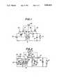
- FIG. 1is a circuit diagram of an embodiment of the power source means according to the invention.
- FIG. 2 through FIG. 4are circuit diagrams of different embodiments of the power source means according to the invention.
- FIG. 5 and FIG. 6are circuit diagrams of power source means of the prior art.
- FIG. 7A and FIG. 7Bare graphs showing oscillatory voltages generated across different elements of the power source means of FIG. 6, respectively.
- 1, 10are direct current (DC) sources; 2 is a switch; 3, 12 are transformers; 4 is a diode; 5, 14 are output capacitors; 6, 15 are loads; 7 is a field effect transistor (FET); 11, 20, 32, 33, 42, 43 are main switching elements; 13, 21, 22, 30, 31, 40, 41 are secondary-side switching elements; 16, 18, 25, 26, 28 are capacitors; 17, 19, 23, 24, 27 are auxiliary switching elements; 29 is a switching element; 35, 36, 37, 38, 53, 54 are auxiliary switching elements; 46, 47, 48, 49, 51, 52 are capacitors; and 50 and 50' are control elements.
- DCdirect current
- FIG. 1is a circuit diagram showing the configuration of an embodiment of the power source means according to the invention.
- a main switching element 11is connected between a DC source 10 and the primary winding 12a of a transformer 12.
- the main switching element 11is an FET.
- a secondary-side switching element 13is connected between the secondary winding 12b of the transformer 12 and an output capacitor 14, which secondary-side switching element 13 is a diode in this embodiment.
- a load 15is connected across the output capacitor 14. It is important in the invention to prevent occurrence of surge voltage at the time of ON-OFF switching of the main switching element 11 by connecting a shunt circuit across the main switching element 11, which shunt circuit is a serial circuit made of a capacitor 16 and an auxiliary switching element 17.
- the auxiliary switching element 17is also an FET in the illustrated embodiment.
- a secondary-side shunt circuitis connected across the secondary-side switching element 13, which secondary-side shunt circuit is a serial circuit made of a capacitor 18 and an auxiliary switching element 19.
- an FETis used as the auxiliary switching element 19.
- the main switching element 11 and the two auxiliary switching elements 17, 19are connected to a control element 50.
- the control element 50is such that, when the main switching element 11 is turned ON or made conductive, the auxiliary switching element 17 is turned OFF or made non-conductive, and when the main switching element 11 is turned OFF or made non-conductive, the auxiliary switching element 17 is turned ON or made conductive.
- the secondary-side switching element 13such as the diode is turned ON or conductive
- the auxiliary switching element 19such as the FET is turned OFF or made non-conductive, and when the secondary-side switching element 13 is turned OFF or non-conductive, the auxiliary switching element 19 is turned ON or made conductive.
- the static capacitance of the capacitor 16 in the shunt circuit for the main switching element 11such as the FET is at least ten times, preferably several tens of times, as large as the parasitic capacitance of the main switching element 11.
- the static capacitance of the capacitor 16may be selected at about 0.1 ⁇ F.
- the static capacitance of the capacitor 18 in the shunt circuit for the secondary-side switching element 13such as the diode is at least ten times, preferably several tens of times, as large as the parasitic capacitance of the secondary-side switching element 13.
- the main switching element 11repeats the switching operations at a desired repetition frequency, and a pulse-width-modulated rectangular voltage is induced in the secondary winding 12b of the transformer 12.
- the auxiliary switching element 17is turned ON or made conductive so as to short circuit the main switching element 11 through a low impedance at low frequencies.
- the capacitor 16 in the shunt circuit for the main switching element 11has a static capacitance which is at least ten times, preferably several tens of times, as large as the parasitic capacitance of the main switching element 11.
- the resonant frequency of the primary winding circuit of the transformer 12becomes lower than that with the parasitic capacitance of the main switching element 11 alone.
- the resonant frequencyshould be only about one tenth or smaller of that without the shunt circuit having capacitor 16, and the voltage across the main switching element 11 is kept substantially constant.
- the main switching element 11when the main switching element 11 is turned ON, that is, made conductive from the non-conductive state, the auxiliary switching element 17 is turned OFF and the voltage of the capacitor 16 is held at the level it had when the switch 17 was turned off. Thus, there is no power loss in the capacitor 16 when the main switching element 11 is conductive.
- the shunt circuit of the secondary-side switching element 13, or a diode in the case of FIG. 1,functions similarly. More specifically, when the secondary-side switching element 13 is turned OFF from its conductive state, the auxiliary switching element 19 is turned ON so as to close the shunt circuit through the capacitor 18 which has a large static capacitance. Hence, even when resonance is caused between the capacitor 18 of the shunt circuit and the leakage inductance of the transformer secondary winding 12b, the resonant frequency is very low, and the voltage across the secondary-side switching element 13 is kept substantially constant and occurrence of a surge voltage is prevented.
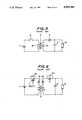
- FIG. 2shows another embodiment of the power source means according to the invention. Like parts to those of FIG. 1 are designated by like numerals.
- This embodimentrepresents a forward type power source means with the shunt circuit of the invention.
- a main switching element 20is connected to the primary side of the transformer 12.
- Two secondary-side switching elements 21 and 22are provided on the secondary-side of the transformer 12; i.e., the switch element 22 is in series with the secondary winding 12b of the transformer, and the switching element 21 shunts the secondary winding 12b of transformer 12 through the switching element 22.
- the secondary-side switching element 21is controlled by a control element 50 similar to that of FIG. 1 so as to operate in an opposite manner to the main switching element 20; namely, when one of the two switching elements is conductive, the other is non-conductive.
- the other secondary-side switching element 22is controlled so that its operation substantially corresponds to that of the main switching element 20.
- each of the switching elements 20, 21 and 22has a shunt circuit formed of capacitors 25, 26, 28, respectively, and an auxiliary switching elements 23, 24, 27 (e.g., an FET) connected in series thereto.
- Such shunt circuitsare effective in preventing the occurrence of the above-mentioned voltage surge.
- FIG. 3shows another embodiment of the invention, in which an AC voltage is produced by an inverter circuit and the AC voltage is applied to a transformer, and secondary-side switching elements (diodes) 30, 31 rectify the induced secondary-side voltage so as to produce a DC output voltage.
- each of the main switching elements (i.e., inverter switches) 32, 33 and the secondary-side switching element 30, 31has a shunt circuit, which shunt circuit is formed of a serial circuit having capacitors 48, 49, 51, 52 and auxiliary switching elements 35, 36, 37, 38 (e.g., an FET) connected thereto.
- the shunt circuitsare effective in preventing the occurrence of a voltage surge at the time of the switching operation.
- FIG. 4shows another power source means according to the invention, which also includes an inverter.
- an AC voltageis produced by a full-bridge type inverter circuit and the AC voltage is applied to a transformer, and secondary-side switching elements (diodes) 40, 41 rectify the induced secondary-side voltage so as to produce a DC output voltage, All the switching elements 35, 36, 37, 38, 53, 54 are connected to a control element 50' similar to element 50 of FIG. 1.
- Two main switching elements (inverter switches) 42 and 44are controlled so as to form a pair wherein when one switching element is conductive the other switching element is non-conductive.
- Other two main switching elements (inverter switches) 43, 45are controlled so as to form a similar pair.
- the control elementoperates the above switching elements while regulating the phase difference between the two pairs of main switching elements, i.e. the pair of 42, 44 and the other pair of 43, 45, so as to regulate the pulse width of the pulse-width-modulated output of the transformer 12.
- each of the main switching elements (i.e., inverter switches) 42, 43, 44, 45 and the secondary-side switching element 40, 41has a shunt circuit, which shunt circuits are formed of serial circuits having large-capacitance capacitors 46, 47, 48, 49 and 51, 52 and auxiliary switching elements 35, 36, 37, 38, 53, 54 (e.g., an FET) connected thereto.
- shunt circuitssubstantially prevent the occurrence of a voltage surge at the time of the switching operation.
- the FET which is used as the switching element in the illustrated embodimentsmay be replaced by a bipolar transistor or a thyristor.
- each of the main and secondary-side switching elementswhen turned OFF to a non-conductive state, it is shunted by a low impedance circuit with a low resonant frequency, which shunting is effective in preventing the occurrence of a voltage surge.
- power efficiency in the power source meansis enhanced and the switching noise is reduced, so as to improve the durability of the various circuit elements.
- the inventionfacilitates the use of a higher switching frequency of the power source means as compared with that of the conventional power source means.
Landscapes
- Engineering & Computer Science (AREA)
- Power Engineering (AREA)
- Dc-Dc Converters (AREA)
- Power Conversion In General (AREA)
Abstract
Description
D=(ON time of switch 2)/(repetition period T)
Eo=(nEiD)/(1-D)
Claims (6)
Applications Claiming Priority (2)
| Application Number | Priority Date | Filing Date | Title |
|---|---|---|---|
| JP1-228194 | 1989-09-05 | ||
| JP1228194AJPH0734653B2 (en) | 1989-09-05 | 1989-09-05 | Power supply |
Publications (1)
| Publication Number | Publication Date |
|---|---|
| US5099406Atrue US5099406A (en) | 1992-03-24 |
Family
ID=16872681
Family Applications (1)
| Application Number | Title | Priority Date | Filing Date |
|---|---|---|---|
| US07/547,286Expired - LifetimeUS5099406A (en) | 1989-09-05 | 1990-07-03 | Dc-dc converter with surge voltage prevention |
Country Status (7)
| Country | Link |
|---|---|
| US (1) | US5099406A (en) |
| EP (1) | EP0416721B1 (en) |
| JP (1) | JPH0734653B2 (en) |
| AU (1) | AU611342B2 (en) |
| CA (1) | CA2020433C (en) |
| DE (1) | DE69009359T2 (en) |
| RU (1) | RU2046526C1 (en) |
Cited By (28)
| Publication number | Priority date | Publication date | Assignee | Title |
|---|---|---|---|---|
| WO1994005076A1 (en)* | 1992-08-25 | 1994-03-03 | Square D Company | Dc to dc/dc to ac power conversion system |
| US5293111A (en)* | 1991-01-22 | 1994-03-08 | Agence Spatiale Europeenne | Method for minimizing the switching loss in a power switch |
| US5303138A (en)* | 1993-04-29 | 1994-04-12 | At&T Bell Laboratories | Low loss synchronous rectifier for application to clamped-mode power converters |
| US5317496A (en)* | 1989-12-19 | 1994-05-31 | Seiersen Ole S | DC/DC-converter with a primary circuit and at least one secondary circuit tuned as individually oscillatory circuits |
| US5327333A (en)* | 1992-11-25 | 1994-07-05 | At&T Bell Laboratories | Push push DC-DC reduced/zero voltage switching converter with off-set tapped secondary winding |
| US5363289A (en)* | 1992-12-15 | 1994-11-08 | At&T Bell Laboratories | Control apparatus for limiting voltage on a core reset capacitor |
| WO1995008863A1 (en)* | 1993-09-22 | 1995-03-30 | Nokia Telecommunications Oy | Flyback-type switched-mode power supply |
| US5455757A (en)* | 1994-01-28 | 1995-10-03 | Compaq Computer Corp. | Power converter having regeneration circuit for reducing oscillations |
| US5490055A (en)* | 1993-03-03 | 1996-02-06 | At&T Corp. | Multiloop feedback control apparatus for DC/DC converters with frequency-shaping band pass current control |
| US5619402A (en)* | 1996-04-16 | 1997-04-08 | O2 Micro, Inc. | Higher-efficiency cold-cathode fluorescent lamp power supply |
| US5621625A (en)* | 1994-08-25 | 1997-04-15 | Samsung Electronics Co., Ltd. | Surge protection circuit for a switching mode power supply |
| US5636108A (en)* | 1995-01-13 | 1997-06-03 | Sextant Avionique | DC-to-DC bidirectional voltage converters and current sensor |
| US5745351A (en)* | 1995-01-13 | 1998-04-28 | Sextant Avionique | DC-to-DC bidirectional voltage converters and current sensor |
| WO1999019974A3 (en)* | 1997-10-15 | 1999-06-24 | Reliance Electric Ind Co | Power loss reduction in power conversion circuitry |
| US6016261A (en)* | 1998-02-03 | 2000-01-18 | U.S. Philips Corporation | Switching voltage converter with synchronous rectification |
| US6021051A (en)* | 1998-12-29 | 2000-02-01 | General Electric Company | Power converter with crowbar circuit and control for very fast output voltage turn-off |
| US6081432A (en)* | 1998-05-26 | 2000-06-27 | Artesyn Technologies, Inc. | Active reset forward converter employing synchronous rectifiers |
| USRE37510E1 (en) | 1995-05-25 | 2002-01-15 | Lucent Technologies Inc. | Self-synchronized drive circuit for a synchronized rectifier in a clamped-mode power converter |
| US6373726B1 (en)* | 1999-01-28 | 2002-04-16 | Power-One A.G. | Flyback converter with transistorized rectifier controlled by primary side control logic |
| US6407934B1 (en)* | 2000-05-31 | 2002-06-18 | Matsushita Electric Industrial Co., Ltd. | DC/DC switching power supply with optimally timed synchronous rectifier |
| US6424544B1 (en)* | 1998-05-07 | 2002-07-23 | Telefonaktiebolaget Lm Ericsson | Continuous mode flyback converter |
| US6460168B1 (en) | 1998-04-23 | 2002-10-01 | Matsushita Electric Industrial Co., Ltd. | Method of designing power supply circuit and semiconductor chip |
| US6882548B1 (en)* | 2003-02-24 | 2005-04-19 | Tyco Electronics Power Systems, Inc. | Auxiliary active clamp circuit, a method of clamping a voltage of a rectifier switch and a power converter employing the circuit or method |
| US20060131961A1 (en)* | 2004-11-19 | 2006-06-22 | Matsushita Electric Industrial Co., Ltd. | Multi-output power supply circuit |
| US7558083B2 (en) | 1997-01-24 | 2009-07-07 | Synqor, Inc. | High efficiency power converter |
| US7564702B2 (en) | 1997-01-24 | 2009-07-21 | Synqor, Inc. | High efficiency power converter |
| US20100019705A1 (en)* | 2008-07-28 | 2010-01-28 | Denso Corporation | Electric power conversion circuit, and control device for multiphase electric rotary machine |
| US10199950B1 (en) | 2013-07-02 | 2019-02-05 | Vlt, Inc. | Power distribution architecture with series-connected bus converter |
Families Citing this family (4)
| Publication number | Priority date | Publication date | Assignee | Title |
|---|---|---|---|---|
| US5434768A (en)* | 1993-02-12 | 1995-07-18 | Rompower | Fixed frequency converter switching at zero voltage |
| ES2157784B1 (en)* | 1999-05-06 | 2002-02-16 | Cit Alcatel | POWER CONVERTER SWITCHED TO ZERO VOLTAGE. |
| RU2224351C2 (en)* | 2001-07-24 | 2004-02-20 | ООО "Аргонавт - ПЛЮС" | Electronic transformer |
| DE10156763A1 (en)* | 2001-11-19 | 2003-06-05 | Siemens Ag | Arrangement for DC / DC conversion |
Citations (8)
| Publication number | Priority date | Publication date | Assignee | Title |
|---|---|---|---|---|
| DE1956145A1 (en)* | 1969-11-07 | 1971-05-19 | Siemens Ag | Circuit for suppressing voltage peaks on transistors |
| US3621363A (en)* | 1968-10-16 | 1971-11-16 | Sven N J Ginnman | An arrangement for premagnetizing a static dc converter |
| SU883339A2 (en)* | 1979-02-06 | 1981-11-23 | Северо-Кавказский Государственный Научно-Исследовательский И Проектный Институт Нефтяной Промышленности | Device for suspending flush casing strings |
| US4336587A (en)* | 1981-06-29 | 1982-06-22 | Boettcher Jr Charles W | High efficiency turn-off loss reduction network with active discharge of storage capacitor |
| US4441146A (en)* | 1982-02-04 | 1984-04-03 | Vicor Corporation | Optimal resetting of the transformer's core in single ended forward converters |
| US4607322A (en)* | 1984-09-17 | 1986-08-19 | Sundstrand Corporation | Energy recovery snubber |
| US4618919A (en)* | 1984-10-04 | 1986-10-21 | Sperry Corporation | Topology for miniature power supply with low voltage and low ripple requirements |
| US4809148A (en)* | 1987-10-21 | 1989-02-28 | British Columbia Telephone Company | Full-fluxed, single-ended DC converter |
Family Cites Families (4)
| Publication number | Priority date | Publication date | Assignee | Title |
|---|---|---|---|---|
| DE2632423C3 (en)* | 1976-07-19 | 1979-09-13 | Siemens Ag, 1000 Berlin Und 8000 Muenchen | Transistor flow converters |
| EP0104278A1 (en)* | 1982-09-29 | 1984-04-04 | Johannes Mannessen | Combustion engine comprising a vaporizer-pressure regulator |
| JPS6351584U (en)* | 1986-09-18 | 1988-04-07 | ||
| JP2656625B2 (en)* | 1989-07-25 | 1997-09-24 | コーセル株式会社 | Resonant converter |
- 1989
- 1989-09-05JPJP1228194Apatent/JPH0734653B2/ennot_activeExpired - Lifetime
- 1990
- 1990-07-03DEDE69009359Tpatent/DE69009359T2/ennot_activeExpired - Fee Related
- 1990-07-03USUS07/547,286patent/US5099406A/ennot_activeExpired - Lifetime
- 1990-07-03EPEP90307253Apatent/EP0416721B1/ennot_activeExpired - Lifetime
- 1990-07-03AUAU58663/90Apatent/AU611342B2/ennot_activeCeased
- 1990-07-04CACA002020433Apatent/CA2020433C/ennot_activeExpired - Fee Related
- 1990-07-23RUSU904830666Apatent/RU2046526C1/ennot_activeIP Right Cessation
Patent Citations (8)
| Publication number | Priority date | Publication date | Assignee | Title |
|---|---|---|---|---|
| US3621363A (en)* | 1968-10-16 | 1971-11-16 | Sven N J Ginnman | An arrangement for premagnetizing a static dc converter |
| DE1956145A1 (en)* | 1969-11-07 | 1971-05-19 | Siemens Ag | Circuit for suppressing voltage peaks on transistors |
| SU883339A2 (en)* | 1979-02-06 | 1981-11-23 | Северо-Кавказский Государственный Научно-Исследовательский И Проектный Институт Нефтяной Промышленности | Device for suspending flush casing strings |
| US4336587A (en)* | 1981-06-29 | 1982-06-22 | Boettcher Jr Charles W | High efficiency turn-off loss reduction network with active discharge of storage capacitor |
| US4441146A (en)* | 1982-02-04 | 1984-04-03 | Vicor Corporation | Optimal resetting of the transformer's core in single ended forward converters |
| US4607322A (en)* | 1984-09-17 | 1986-08-19 | Sundstrand Corporation | Energy recovery snubber |
| US4618919A (en)* | 1984-10-04 | 1986-10-21 | Sperry Corporation | Topology for miniature power supply with low voltage and low ripple requirements |
| US4809148A (en)* | 1987-10-21 | 1989-02-28 | British Columbia Telephone Company | Full-fluxed, single-ended DC converter |
Cited By (42)
| Publication number | Priority date | Publication date | Assignee | Title |
|---|---|---|---|---|
| US5317496A (en)* | 1989-12-19 | 1994-05-31 | Seiersen Ole S | DC/DC-converter with a primary circuit and at least one secondary circuit tuned as individually oscillatory circuits |
| US5293111A (en)* | 1991-01-22 | 1994-03-08 | Agence Spatiale Europeenne | Method for minimizing the switching loss in a power switch |
| WO1994005076A1 (en)* | 1992-08-25 | 1994-03-03 | Square D Company | Dc to dc/dc to ac power conversion system |
| US5327333A (en)* | 1992-11-25 | 1994-07-05 | At&T Bell Laboratories | Push push DC-DC reduced/zero voltage switching converter with off-set tapped secondary winding |
| US5363289A (en)* | 1992-12-15 | 1994-11-08 | At&T Bell Laboratories | Control apparatus for limiting voltage on a core reset capacitor |
| US5490055A (en)* | 1993-03-03 | 1996-02-06 | At&T Corp. | Multiloop feedback control apparatus for DC/DC converters with frequency-shaping band pass current control |
| USRE36571E (en)* | 1993-04-29 | 2000-02-15 | Lucent Technologies Inc. | Low loss synchronous rectifier for application to clamped-mode power converters |
| US5303138A (en)* | 1993-04-29 | 1994-04-12 | At&T Bell Laboratories | Low loss synchronous rectifier for application to clamped-mode power converters |
| WO1995008863A1 (en)* | 1993-09-22 | 1995-03-30 | Nokia Telecommunications Oy | Flyback-type switched-mode power supply |
| GB2297397A (en)* | 1993-09-22 | 1996-07-31 | Nokia Telecommunications Oy | Flyback-type switched-mode power supply |
| GB2297397B (en)* | 1993-09-22 | 1997-03-26 | Nokia Telecommunications Oy | Flyback-type switched-mode power supply |
| US5455757A (en)* | 1994-01-28 | 1995-10-03 | Compaq Computer Corp. | Power converter having regeneration circuit for reducing oscillations |
| US5621625A (en)* | 1994-08-25 | 1997-04-15 | Samsung Electronics Co., Ltd. | Surge protection circuit for a switching mode power supply |
| US5636108A (en)* | 1995-01-13 | 1997-06-03 | Sextant Avionique | DC-to-DC bidirectional voltage converters and current sensor |
| US5745351A (en)* | 1995-01-13 | 1998-04-28 | Sextant Avionique | DC-to-DC bidirectional voltage converters and current sensor |
| USRE37510E1 (en) | 1995-05-25 | 2002-01-15 | Lucent Technologies Inc. | Self-synchronized drive circuit for a synchronized rectifier in a clamped-mode power converter |
| US5619402A (en)* | 1996-04-16 | 1997-04-08 | O2 Micro, Inc. | Higher-efficiency cold-cathode fluorescent lamp power supply |
| US7558083B2 (en) | 1997-01-24 | 2009-07-07 | Synqor, Inc. | High efficiency power converter |
| US7564702B2 (en) | 1997-01-24 | 2009-07-21 | Synqor, Inc. | High efficiency power converter |
| US9143042B2 (en) | 1997-01-24 | 2015-09-22 | Synqor, Inc. | High efficiency power converter |
| US8493751B2 (en) | 1997-01-24 | 2013-07-23 | Synqor, Inc. | High efficiency power converter |
| US8023290B2 (en) | 1997-01-24 | 2011-09-20 | Synqor, Inc. | High efficiency power converter |
| WO1999019974A3 (en)* | 1997-10-15 | 1999-06-24 | Reliance Electric Ind Co | Power loss reduction in power conversion circuitry |
| US5943223A (en)* | 1997-10-15 | 1999-08-24 | Reliance Electric Industrial Company | Electric switches for reducing on-state power loss |
| US6016261A (en)* | 1998-02-03 | 2000-01-18 | U.S. Philips Corporation | Switching voltage converter with synchronous rectification |
| US6684378B2 (en) | 1998-04-23 | 2004-01-27 | Matsushita Electric Industrial Co., Ltd. | Method for designing power supply circuit and semiconductor chip |
| US6460168B1 (en) | 1998-04-23 | 2002-10-01 | Matsushita Electric Industrial Co., Ltd. | Method of designing power supply circuit and semiconductor chip |
| US6424544B1 (en)* | 1998-05-07 | 2002-07-23 | Telefonaktiebolaget Lm Ericsson | Continuous mode flyback converter |
| US6081432A (en)* | 1998-05-26 | 2000-06-27 | Artesyn Technologies, Inc. | Active reset forward converter employing synchronous rectifiers |
| US6252781B1 (en) | 1998-05-26 | 2001-06-26 | Artesyn Technologies, Inc. | Active reset forward converter employing synchronous rectifiers |
| US6021051A (en)* | 1998-12-29 | 2000-02-01 | General Electric Company | Power converter with crowbar circuit and control for very fast output voltage turn-off |
| US6373726B1 (en)* | 1999-01-28 | 2002-04-16 | Power-One A.G. | Flyback converter with transistorized rectifier controlled by primary side control logic |
| US6407934B1 (en)* | 2000-05-31 | 2002-06-18 | Matsushita Electric Industrial Co., Ltd. | DC/DC switching power supply with optimally timed synchronous rectifier |
| US6882548B1 (en)* | 2003-02-24 | 2005-04-19 | Tyco Electronics Power Systems, Inc. | Auxiliary active clamp circuit, a method of clamping a voltage of a rectifier switch and a power converter employing the circuit or method |
| US20060131961A1 (en)* | 2004-11-19 | 2006-06-22 | Matsushita Electric Industrial Co., Ltd. | Multi-output power supply circuit |
| US8154236B2 (en)* | 2008-07-28 | 2012-04-10 | Denso Corporation | Electric power conversion circuit, and control device for multiphase electric rotary machine |
| US20100019705A1 (en)* | 2008-07-28 | 2010-01-28 | Denso Corporation | Electric power conversion circuit, and control device for multiphase electric rotary machine |
| US10199950B1 (en) | 2013-07-02 | 2019-02-05 | Vlt, Inc. | Power distribution architecture with series-connected bus converter |
| US10594223B1 (en) | 2013-07-02 | 2020-03-17 | Vlt, Inc. | Power distribution architecture with series-connected bus converter |
| US11075583B1 (en) | 2013-07-02 | 2021-07-27 | Vicor Corporation | Power distribution architecture with series-connected bus converter |
| US11705820B2 (en) | 2013-07-02 | 2023-07-18 | Vicor Corporation | Power distribution architecture with series-connected bus converter |
| US12395087B1 (en) | 2013-07-02 | 2025-08-19 | Vicor Corporation | Power distribution architecture with series-connected bus converter |
Also Published As
| Publication number | Publication date |
|---|---|
| AU5866390A (en) | 1991-03-14 |
| JPH0393466A (en) | 1991-04-18 |
| AU611342B2 (en) | 1991-06-06 |
| EP0416721A1 (en) | 1991-03-13 |
| DE69009359D1 (en) | 1994-07-07 |
| EP0416721B1 (en) | 1994-06-01 |
| CA2020433A1 (en) | 1991-03-06 |
| JPH0734653B2 (en) | 1995-04-12 |
| DE69009359T2 (en) | 1994-09-15 |
| RU2046526C1 (en) | 1995-10-20 |
| CA2020433C (en) | 1995-12-26 |
Similar Documents
| Publication | Publication Date | Title |
|---|---|---|
| US5099406A (en) | Dc-dc converter with surge voltage prevention | |
| EP0336725B1 (en) | Switching power supply | |
| US5796598A (en) | Voltage-converting circuit for the power supply of an electrical consumer of high output, particularly a bobbin winding machine | |
| US4814962A (en) | Zero voltage switching half bridge resonant converter | |
| EP0480575B1 (en) | Lossless snubber | |
| US6587358B1 (en) | Switching power supply circuit | |
| US4785387A (en) | Resonant converters with secondary-side resonance | |
| US4860184A (en) | Half-bridge zero-voltage switched multi-resonant converters | |
| US5943224A (en) | Post regulator with energy recovery snubber and power supply employing the same | |
| Oruganti et al. | Soft-switched DC/DC converter with PWM control | |
| US5508904A (en) | Switching regulator having superimposing chopping-wave voltage forming circuit | |
| JP3351400B2 (en) | Switching power supply | |
| KR0144540B1 (en) | Surge Protection Circuits in Switched-Mode Power Supplies | |
| US4654771A (en) | Switched power supply comprising a free-running flow converter and electrically separated control loop | |
| JPH02184267A (en) | Series resonance inverter with non-loss snabber-reset part | |
| US4486822A (en) | Switched-mode self oscillating supply voltage circuit | |
| KR20030069052A (en) | Switching power supply circuit | |
| EP0058401B1 (en) | High frequency switching circuit | |
| US5640310A (en) | Current resonance type switching power source | |
| US4453205A (en) | DC/AC Converter with shunt regulated load | |
| US4277824A (en) | Start-up circuit | |
| US6504734B2 (en) | Switched power converter utilizing a piezoelectric transformer | |
| US4250541A (en) | Push-push resonant power inverter | |
| US5327334A (en) | Zero current switching DC-DC converter incorporating a tapped resonant inductor | |
| US4464710A (en) | Simplified d.c. to d.c. converter |
Legal Events
| Date | Code | Title | Description |
|---|---|---|---|
| AS | Assignment | Owner name:KYUSHU UNIVERSITY, JAPAN Free format text:ASSIGNMENT OF ASSIGNORS INTEREST.;ASSIGNORS:HARADA, KOSUKE;SAKAMOTO, HIROSHI;REEL/FRAME:005452/0527 Effective date:19900626 | |
| STCF | Information on status: patent grant | Free format text:PATENTED CASE | |
| FEPP | Fee payment procedure | Free format text:PAYOR NUMBER ASSIGNED (ORIGINAL EVENT CODE: ASPN); ENTITY STATUS OF PATENT OWNER: SMALL ENTITY | |
| FPAY | Fee payment | Year of fee payment:4 | |
| FEPP | Fee payment procedure | Free format text:PAYER NUMBER DE-ASSIGNED (ORIGINAL EVENT CODE: RMPN); ENTITY STATUS OF PATENT OWNER: SMALL ENTITY | |
| FPAY | Fee payment | Year of fee payment:8 | |
| FEPP | Fee payment procedure | Free format text:PAYER NUMBER DE-ASSIGNED (ORIGINAL EVENT CODE: RMPN); ENTITY STATUS OF PATENT OWNER: SMALL ENTITY Free format text:PAYOR NUMBER ASSIGNED (ORIGINAL EVENT CODE: ASPN); ENTITY STATUS OF PATENT OWNER: SMALL ENTITY | |
| FPAY | Fee payment | Year of fee payment:12 | |
| FEPP | Fee payment procedure | Free format text:PAYER NUMBER DE-ASSIGNED (ORIGINAL EVENT CODE: RMPN); ENTITY STATUS OF PATENT OWNER: SMALL ENTITY Free format text:PAYOR NUMBER ASSIGNED (ORIGINAL EVENT CODE: ASPN); ENTITY STATUS OF PATENT OWNER: SMALL ENTITY |