US5097422A - Method and apparatus for designing integrated circuits - Google Patents
Method and apparatus for designing integrated circuitsDownload PDFInfo
- Publication number
- US5097422A US5097422AUS07/374,485US37448589AUS5097422AUS 5097422 AUS5097422 AUS 5097422AUS 37448589 AUS37448589 AUS 37448589AUS 5097422 AUS5097422 AUS 5097422A
- Authority
- US
- United States
- Prior art keywords
- integrated circuit
- design rule
- defining
- layout
- layers
- Prior art date
- Legal status (The legal status is an assumption and is not a legal conclusion. Google has not performed a legal analysis and makes no representation as to the accuracy of the status listed.)
- Expired - Fee Related
Links
Images


Classifications
- G—PHYSICS
- G06—COMPUTING OR CALCULATING; COUNTING
- G06F—ELECTRIC DIGITAL DATA PROCESSING
- G06F30/00—Computer-aided design [CAD]
- G06F30/30—Circuit design
- G06F30/39—Circuit design at the physical level
Definitions
- This inventionrelates to integrated circuit design tools. More particularly, this invention relates to a symbolic and dynamic method for designing integrated circuits and an apparatus for implementing such method.
- a monolithic integrated circuitis a combination of interconnected circuit elements inseparably associated on or within a continuous substrate.
- the circuit elementsare conventional components--transistors, diodes, capacitors, and resistors--fabricated in situ within or on a single crystal of semiconductor material with the capability of performing a complete electronic circuit function.
- an integrated circuitis designed in a top-down method by first designing a logic level drawing and a transistor level drawing. These drawings then are used to design the more detailed integrated circuit layout, which shows the IC layers (i.e., metal, polysilicon, active, and the ways they interrelate to form transistor gates, wires, contact points, etc.).
- the integrated circuit layoutoften referred to as "geometry,” is used to generate the integrated circuit tooling, which is a series of masks, each representing a layer for the integrated circuit. The tooling is then used by manufacturers to fabricate an integrated circuit.
- Photolithographyis any technique whereby light or other electromagnetic rays are shown through a mask to create a pattern on a silicon wafer coated with a photosensitive film.
- Dopingincludes those techniques for treating the exposed areas in the pattern to take on n- or p-type characteristics to form components of transistors and diodes.
- Metal depositionrefers to the growth or deposit of photoresist, insulating oxide, metal, polysilicon, and other materials that form the topology of the circuit.
- a layer of photoresistive materialis deposited on a semiconductor wafer.
- a mask for the integrated circuitis then placed over the layer of photoresistive material and light is shown through the mask to activate parts of the photoresistive material, thereby leaving a predetermined pattern of conductors on the wafer and exposed areas of the wafer between the conductors.
- Transistors and diodesare then formed by doping portions the exposed areas of the wafer with a chemical doping agent.
- a second maskcan then be used to generate another pattern of conductors and exposed areas which are, once again, doped. Additional doping layers may also be used. After each doping step, the photoresistive material is chemically removed from the wafer.
- a pattern of exposed areas of the waferis once again formed by exposing a layer of photoresist on the wafer through a mask.
- a layer of metal or other suitable conductoris then deposited onto portions of the exposed areas of the semiconductor wafer to form the desired interconnections between components on the wafer.
- Design rulesinclude, for example, specifications for minimum spacing between transistors and minimum separation between conductors to prevent shorting, specifications for minimum metal width, and specifications for maximum metal heights and slopes of walls which form metal junctions.
- design rulesare changing to allow for smaller and smaller spacings between materials on an integrated circuit and to allow smaller and smaller substrate areas.
- design rulesmay change during the development process of any particular circuits. Because increases in the die size of a mask by 15% typically result in a doubling of the cost of an integrated circuit, minimal substrate areas are desired.
- An object of this inventionis to provide a method and an apparatus for designing integrated circuits which are independent of the design rule constraints of conventional materials and fabrication technologies and techniques.
- Another object of this inventionis to provide a method and an apparatus for designing integrated circuits which minimize the area of a circuit layout for any given electronic circuit design, including highly complex, custom-designed integrated circuits.
- a further object of this inventionis to provide a method and an apparatus for designing integrated circuits that automate the design process so that highly complex, custom-integrated circuits can be economically produced in a relatively short time.
- a still further object of this inventionis to provide a method and an apparatus for designing integrated circuits which can be used to create electronic circuit design "building blocks,” which in turn can be used for designing highly complex integrated circuits.
- Yet another object of this inventionis to provide a method and an apparatus for designing integrated circuits which require minimal integrated circuit design expertise in operation.
- the gridis defined in relative terms, such that an origin along an x axis and an origin along a y axis are used to define reference points from which all positions on the grid are defined. These reference points are relative positions defined in terms of the origin or other reference points along the same axis, and/or one or more design rule variables.
- Integrated circuit componentscontacts, gates, wires, etc.
- a specific layoutis defined by specifying values for the design rule variables, thereby fixing the positions of the integrated circuit components.
- the method describedrefers to relatively positioning integrated circuit components and to design rule variables corresponding to positioning constraints for various fabrication technologies and techniques, the method could also be used for relatively positioning other objects and for design rule variables corresponding to other positioning constraints.
- the methodis used for designing subportions of an integrated circuit which are then integrated to form an entire integrated circuit layout database.
- the databaseis used to form tooling and/or masks for conventional fabrication processes.
- the subportionsmay be strategically designed by function, so the geometry may be used as an interchangeable module for various integrated circuit layouts or as a building block in highly complex integrated circuits.
- module compilationis commonly referred to as "module compilation.”
- One apparatus for implementing this inventionis a computer system used to host software tools for designing integrated circuits.
- a subset of the software tools and the methodology for using such subsetcombine to be the preferred embodiment of the method of this invention.
- the computer systemis used to automate the design process and might include additional software tools for integrating modules, simulating integrated circuit performance, printing geometries, and creating tooling (such as masks).
- FIG. 1is an isometric view of an embodiment of the apparatus for designing integrated circuits.
- FIG. 2is a flow chart for designing an integrated circuit module compiler using the apparatus of FIG. 1.
- FIG. 3is a sample gate level schematic of one cell of a clocked dynamic shift register.
- FIG. 4is a sample discrete device level schematic of one cell of a clocked dynamic shift register.
- FIG. 5is a sample hand-drawn geometry layout of a clocked dynamic shift register.
- FIG. 6is a sample schematic symbol for an eight-bit clocked dynamic shift register.
- FIG. 7is a flow chart showing the steps performed by the compiler-link editor when generating an executable module compiler for producing the integrated circuit layout geometry.
- FIG. 8is a schematic diagram showing the directory file organization for a clocked dynamic shift register of unspecified length.
- FIG. 9is a layout of the geometry generated from the source code of Table 2.
- FIGS. 10A and 10Bare layouts of a shift register cell, expressing the cell in two distinct technologies.
- the preferred embodiment of the apparatus for designing integrated circuits 10is a conventional computer system including a computer 12, terminal 14, printer 16, and plotter 18.
- the computeris a VAX 11/785, model no. 11-785-AA, manufactured by Digital Equipment Corporation (DEC);
- the terminalis an AED 767 monitor terminal manufactured by Advanced Electronic Design, Inc.;
- the printermay be any one of a large number of available models;
- the plotteris an HP 7475A manufactured by Hewlett-Packard, Inc.
- the VAX 11/785uses a UNIX version 4.2 operating system and includes an interface program for the AED 767 monitor called "Caesar version 7," developed at the University of California at Berkeley, and a "C" program language compiler, developed by Bell Laboratories.
- the method for designing integrated circuitsis embodied within a Compiler Development System (CDS).
- CDSCompiler Development System
- the computer system 10includes a set of software tools for designing integrated circuit module compilers, each consisting of source code and executable code.
- the integrated circuit moduleis an array of cells. Each cell, in turn, is the geometric definition of the required integrated circuit components. Every module can be combined, like a building block, with other modules in order to create a complete geometric description of an integrated circuit and a corresponding mask work.
- the preferred embodiment of the methodis, in effect, the implementation of a high level software language referred to as the "Silicon Compiler Software Language for Integrated Circuits" (SLIC).
- SLICSoftware Language for Integrated Circuits
- Each SLIC commandcomprises, in one embodiment, a set of "C" language function calls.
- the preferred embodimentis a language for writing source code which is to be compiled to generate executable code. Execution of the executable code results in a specific geometry layout.
- the module compilermay be used with other module compilers or alone to develop an integrated circuit layout.
- the software tools for developing module compilersare used with other software in packages such as the ConcordeTM VLSI Compiler produced by Seattle Silicon Technology, Inc.
- These other software toolsinclude programs for interconnecting modules, such as the Pride/Auto RouteTM software tool within the ConcordeTM package.
- a modular approachis used for designing a complex integrate circuit.
- the circuit for each moduleis designed, tested, and debugged before it is integrated with other modules to form the complete integrated circuit layout and mask work.
- the preferred embodiment of the methodis a software embodiment designed to run on the VAX 11/785 having a Unix Version 4.2 operating system and a "C" compiler
- other embodiments of the methodcould be software programs designed to run on computer systems using other computers, terminals, printers, and plotters with another operating system and programming language.
- Still other embodiments of the methodneed not take the form of a computer program or be implemented through a computer system.
- SLICis an extension language of the "C" programming language. SLIC is used to write geometry generator source code for generating a layout. A second extension language, GSSLIC, may be used to write simulation model source code for simulating the performance of the layout design. A third extension language, SSSLIC, may be used to write schematic symbol generator source code for deriving a schematic symbol for the module under development (e.g., the logic symbol for an ⁇ OR ⁇ gate with inputs and outputs).
- the designeridentifies the module specification 20, including the technology to be used (e.g., CMOS or BIPOLAR), the functional characteristics of the circuit, a connection diagram, the approximate dimensions, and the end user input options for the integrated circuit module.
- the designerthen develops preliminary high-level drawings of the integrated circuit.
- One drawingtypically, is a gate level drawing 22 specifying the circuits with standard gates and interconnections.
- the gatesare reduced to their discrete devices (i.e., transistors) in a device level drawing 24.
- a preliminary layout drawing 26is then derived, translating the discrete devices into a physical geometry of layers and components, such as wires, contacts, etc.
- a clocked dynamic shift registermight be specified as follows:
- the designwill be implemented in CMOS PWELL technology, with Vdd above, +5 volts, GND below, 0.5 volts.
- the inputwill be placed on the left, the output on the right.
- Each cell (or bit) of the shift registerwill delay an input signal one clock cycle.
- the number of bits, and thus the number of delays,is determined by the designer. There is to be no limit to the number of bits allowed.
- the gate level schematic (drawing 22 in FIG. 2) for one cell of the serial-in, serial-out clocked dynamic shift register specified aboveconsists of two clocked inverters 28, 30, which together have the effect of delaying an input signal one clock cycle.
- a single cell at the discrete device level (drawing 24 in FIG. 2) for the serial-in, serial-out clocked dynamic shift register specified abovecomprises two identical buffers, each consisting of a basic inverter circuit of transistors 32, 34, 36, 38 and 32', 34', 36', 38'.
- the preliminary, manually drawn layout (drawing 26 in FIG. 2) for one cell of the serial-in, serial-out clocked dynamic shift registeris shown, comprising its component metal 40, polysilicon 42, and active (diffusion) region 44, PWELL 46, P+ region 48, and N+ regions 50.
- the input, output, clock signals (CLK1, CLK2), inverted clock signals (CLK1NOT, CLK2NOT), power voltage (Vdd), and ground connections (GND)are all labeled.
- the designerstrategically identifies reference points (X1-X5, Y1-Y9) for forming a dynamic virtual grid.
- Each reference pointis defined along an X axis or a Y axis.
- the reference pointsare defined as all horizontal rows and vertical columns that contain at least one contact (specified by an "X" in FIG. 5).
- These reference pointscan be defined with respect to other landmarks, such as transistor gates, the center of a wire, or other geometric features.
- Design rule variablesare variables specifying configuration constraints, such as metal width, polysilicon width, metal spacing, etc.
- a sample of design rule variables, by no means a complete list,is included below in Table 1.
- the virtual gridmay be abstracted from the reference points to consist of lines crossing each other, wherein the spacing between lines is not determined.
- the gridis not part of the layout, but instead is a virtual grid for dynamically defining relative integrated circuit feature positions.
- the virtual gridis superimposed on a fixed grid of centi- micron units, using the X origin and Y origin as the link between the two grids.
- the fixed griddefines the precision designed into the geometry generator for relatively positioning components on the virtual grid.
- the designermay wish to design a modified gate level drawing 52 (see FIG. 2) as a result of the discovery of advantageous gate level changes that can be made. For example, an alternative way of realizing a given logic function could be discovered at this point.
- the designeralso defines a schematic symbol drawing 54 to be used to represent the module in an overall schematic diagram of an integrated circuit using the shift register. Referring to FIG. 6, a schematic symbol 56 for an eight-bit clocked dynamic shift register is shown.
- the designercan write a computer program using the well-known "C” programming language and SLIC commands to generate a design rule-independent layout rule module compiler.
- the designermay write shell source code 58 in the "C" programming language to define the module, may include a file of design rules, and may also develop an interactive menu to make the completed module compiler "user-friendly.”
- SLIC commandsas geometry generator source code 60.
- This source codedefines the dynamic virtual grid in terms of the reference points shown in FIG. 5.
- Table 2an example of SLIC source code used to define the reference points for one cell of the clocked dynamic shift register specified above is shown in program lines 81-85 and 88-96.
- This examplealso includes shell source code 58. ##SPC1##
- reference pointsare defined using landmark commands.
- landmark x1is defined in terms of the origin
- landmark x3is defined in terms of the x1 landmark and a variable, rtend, which is defined as "the greater of the two design rule variables ⁇ nac2pwc ⁇ ⁇ pac2sbc. ⁇ ”
- nac2pwcmeans the center of an n+ active contact to the center of p+ active contact
- pac2sbcmeans the center of p+ active contact to the center of substrate contact.
- the source code for the clocked dynamic shift register example specified aboveincludes SLIC source code for defining a metal layer (lines 101-129), an active layer (lines 130-140), a polysilicon layer (lines 141-173), the substrate and PWELL contacts (lines 174-181), and all other contacts (lines 182-205), followed by the N+ active layer (lines 206-213), P+ active layer (lines 214-221), PWELL layer (lines 222-229), and the ports (lines 230-249).
- the moduleis defined to include a variable number of cells, "nbits.”
- the features of the integrated circuitare defined in terms of a specified layer, reference points, and design rule variables.
- the power and ground lines, the clock lines, and the transistor connections for the clocked dynamic shift register exampleare each metal features. They are defined using the SLIC "wire" statement.
- the wireis defined using reference points and design rule variables to specify the width of the wire and the X and Y beginning point direction (right-left (X), up-down (Y), diagonal (XY)), and end point (x or y).
- wire (bm, x1, y1); x (x5+rtend), which defines a power linemeans "draw a wire of big metal (bm) width from landmarks x1, y1 in a horizontal direction to x5 plus the value of rtend.”
- rtendis a variable defined as "a function of two design rule variables ⁇ nac2pwc ⁇ and ⁇ pac2sbc. ⁇ "
- commandsare part of the SLIC extension language used for defining layouts: grid commands, primitive geometry commands, contact commands, label commands, draw/place commands, location commands, attribute commands, bounding box commands, and miscellaneous commands. Many of these commands are shown in the listing of Table 2.
- Grid commandsdefine the reference points that form the virtual dynamic grid of the layout drawing (see lines 81-96 in Table 2), thereby describing their virtual geometric relationship.
- the position of a landmarkis usually defined relative to a previously defined landmark other than the first landmark along each axis.
- the first point defined in an axisis usually an origin. This relative definition enables the user to establish a dependency among the landmarks. Thus, when a landmark is moved, subordinate landmarks will move with it, whereas independent landmarks will not.
- Primitive geometry commandsare used for placing a layer, a wire, a polygon, or a box on the virtual dynamic grid and are defined as functions of layer, reference points, and design rule variables. Examples are shown on lines 117-120 of Table 2. Geometry commands enable extension of a wire center, an edge in an X direction or a Y direction, or a diagonal direction by a given length.
- Contact commandsare used to place contact cells at specified coordinates (for example see lines 186-193 and 196-201).
- a contactis a juncture point for joining two layers to provide a conductive path for current flow. Examples are found in lines 186-201 of Table 2.
- Label commandsare used for defining ports, such as power ports, ground ports, input ports, output ports, etc. Illustrations of the label commands can be seen on lines 233-247 of the listing in Table 2. Additionally, there are node label commands for defining nodes used for simulation purposes.
- Location commandsretrieve the a location and size a port. Attribute commands assign attributes to a cell or elements within a cell, such as the location of a port on one side of a module.
- Bounding box commandsare used for defining a cell or module boundary or perimeter.
- the geometry generator, simulation model generator, and schematic symbol generator source codesare compiled and linked (if the latter two codes have been written) using the computer system's "C" compiler and link editor 66 to produce a module compiler 68.
- the module compilerthen generates a geometry database and possibly a simulation model and a schematic symbol databases. These databases are the embodiment of the IC module created. They may be scrutinized by debugging programs, viewed and plotted as geometry, and ultimately converted to a format for mask work generation. To plot the module and layout, the geometry data base is transformed into a format readable by the plotter. The layout of the module is then plotted layer by layer, including the port and node labels.
- FIG. 7is a flow chart showing the steps performed by the compiler-link editor when generating an executable module compiler for producing the integrated circuit layout geometry.
- the compilerconsists of up to four elements: a shell, a geometry generator, a simulation model generator, and a schematic symbol generator. To produce only the integrated circuit layout geometry, the shell and geometry generator are required.
- the compiler shellconsists of a user interface, initialization routines, and, possibly, a scanner, parser, and error handler. In the user interface of the compiler shell, it can seen that the user specifies module name (step 72), design rule set (step 73), and, where applicable, the number of bits required (step 74). In the example of a shift register, the number of bits must be specified.
- step 75the compiler shell passes the specifications of module name and number of bits to the geometry, simulation model, and schematic symbol generators. Rule set and process parameter tables referenced by the specified design rule set (step 73) are passed to the generators in step 76. Entering its initialization routines, the compiler shell then initiates the setup of the integrated circuit module database (step 77).
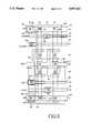
- FIG. 8is a schematic diagram showing the directory file organization of the intergrated circuit module database set up in step 77 (FIG. 7). This organization is illustrated in terms of a clocked dynamic shift register of unspecified length.
- Directory 110is a directory named for the design rule specified (step 73). Within this directory, the initialization routines of the shell compiler create subdirectories sstsim (112) and sstbody (114). The shell compiler then writes to directory sstsim (112) a set of simulation primitives to be used by the simulation model generator.
- File dsr 116are stored under directory sstbody 114.
- Hierarchical files dsr 118, bit0 120, SRsubcell 122, STAGE1 124, and simulation primitive files s . . . 126are stored under directory sstsim 112 to be used in the simulation generator.
- the geometry generatoraccepts the parameters from the user interface and creates the layers (for example, polycrystalline silicon, metal, and active) making up the physical module.
- This layer-by-layer descriptionconstitutes the layout view of the integrated circuit module. This view is written to subdirectory sstif 128, which is created by the geometry generator.
- This directorycontains the hierarchical files dsr 130, bit0 132, SRsubcell 134, and STAGE1 136. Starting at the bottom of the hierarchy, STAGE1 represents only one of the clocked stages required for a shift register subcell.
- File SRsubcell 134contains the next higher description of how copies of STAGE1 (136) are connected.
- bit0 (132)is described in terms of connections of SRsubcell 134, while the highest hierarchical level, file dsr (130), is described in terms of file bit0 (132).
- the geometry generatoralso calls a utility named makefp, which reads the sstif files and extracts from them a footprint description consisting of the module's global bounding box with labeled terminal ports. These data are placed in subdirectory fp 138 in file dsr 140.
- the files specified under the directories shown in FIG. 8are created by a call to the geometry generator (step 78).
- the geometry generatoraccepts parameters from the user interface of the compiler shell in step 79 from which the geometry generator creates a layer-by-layer description of the physical module (step 150).
- Directory sstifis created in step 152 and the layer-by-layer description is distributed to the files 130-136 of directory sstif 128 (154).
- the footprint directoryis extracted from the sstif files in step 156 and stored in file fp in step 158.
- FIG. 9shows a black and white copy of the color plot 70 derived from the source code of Table 2.
- the design rule variablesare fixed at given values, thereby generating a specific version of the integrated circuit layout for the module under development.
- the design rule variablesare defined in the form of a data file accessed during execution. If a version of the module is needed in a different rule set, a design rule variable file containing these new values can be substituted for the original file.
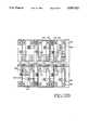
- FIGS. 10A and 10Bshow the same shift register cell as expressed in two different technologies according to the method and apparatus of the present invention. Each cell is arranged as two rows, each row being a three-bit shift register.
- the techology for the shift register shown in FIG. 8Ais 3-micron CMOS, having one metal and one polysilicon layer.
- the dimensions of the layout shown in FIG. 8Aare 120.5 microns horizontally by 98 microns vertically, with a resulting aspect ratio (i.e., height/width) of 0.813.
- FIG. 8Bis a layout of a 2-micron CMOS 3-by-2 shift register cell having two metal and one polycrystalline silicon layer.
- the dimensions of the bounding box of this layoutare 88.06 microns horizontally and 75.42 microns vertically. This produces an aspect ratio of 0.856.
- the design rules of the 3-micron CMOS technology shown in FIG. 8Arequires the polycrystalline silicon area 94 around contact 96 to be spaced apart from active trace 98.
- the polycrystalline silicon area 94' surrounding contact 96'is allowed to abut the active trace 98' according to the design rules of the 2-micron CMOS technology shown in FIG. 8B.
- the metal layer 100 of contact 96coincides with polycrystalline silicon area 94 in FIG. 8A, in the technology of FIG. 8B, the metal area 100' extends beyond the boundaries of area 94'.
- FIGS. 8A and 8BCareful comparison of FIGS. 8A and 8B also shows that contacts designated as areas 102 and 102', respectively, are of distinctly different relative sizes. In particular, in the vicinity of contact 104, contact area 102, metal area 106, and active areas 108 have distinctly different relative sizes than do their counterparts (indicated by primed numbers) in FIG. 8B.
Landscapes
- Engineering & Computer Science (AREA)
- Computer Hardware Design (AREA)
- Physics & Mathematics (AREA)
- Theoretical Computer Science (AREA)
- Evolutionary Computation (AREA)
- Geometry (AREA)
- General Engineering & Computer Science (AREA)
- General Physics & Mathematics (AREA)
- Design And Manufacture Of Integrated Circuits (AREA)
Abstract
Description
This application is a continuation of U.S. application Ser. No. 06/917,917 filed Oct. 10, 1986, now abandonned.
This invention relates to integrated circuit design tools. More particularly, this invention relates to a symbolic and dynamic method for designing integrated circuits and an apparatus for implementing such method.
A monolithic integrated circuit is a combination of interconnected circuit elements inseparably associated on or within a continuous substrate. Typically, the circuit elements are conventional components--transistors, diodes, capacitors, and resistors--fabricated in situ within or on a single crystal of semiconductor material with the capability of performing a complete electronic circuit function.
In practice, an integrated circuit is designed in a top-down method by first designing a logic level drawing and a transistor level drawing. These drawings then are used to design the more detailed integrated circuit layout, which shows the IC layers (i.e., metal, polysilicon, active, and the ways they interrelate to form transistor gates, wires, contact points, etc.). The integrated circuit layout, often referred to as "geometry," is used to generate the integrated circuit tooling, which is a series of masks, each representing a layer for the integrated circuit. The tooling is then used by manufacturers to fabricate an integrated circuit.
Typically, monolithic integrated circuits are fabricated by a process of photolithography, doping, and material deposition. Photolithography is any technique whereby light or other electromagnetic rays are shown through a mask to create a pattern on a silicon wafer coated with a photosensitive film. Doping includes those techniques for treating the exposed areas in the pattern to take on n- or p-type characteristics to form components of transistors and diodes. "Material deposition" refers to the growth or deposit of photoresist, insulating oxide, metal, polysilicon, and other materials that form the topology of the circuit.
In one method for fabricating an integrated circuit, a layer of photoresistive material is deposited on a semiconductor wafer. A mask for the integrated circuit is then placed over the layer of photoresistive material and light is shown through the mask to activate parts of the photoresistive material, thereby leaving a predetermined pattern of conductors on the wafer and exposed areas of the wafer between the conductors. Transistors and diodes are then formed by doping portions the exposed areas of the wafer with a chemical doping agent. A second mask can then be used to generate another pattern of conductors and exposed areas which are, once again, doped. Additional doping layers may also be used. After each doping step, the photoresistive material is chemically removed from the wafer. When the final doping layer has been completed, a pattern of exposed areas of the wafer is once again formed by exposing a layer of photoresist on the wafer through a mask. A layer of metal or other suitable conductor is then deposited onto portions of the exposed areas of the semiconductor wafer to form the desired interconnections between components on the wafer. Though there are many fabrication technologies, fabrication techniques, and integrated circuit materials, fabricating the design for the integrated circuit through one or more masks is used consistently.
Depending on the fabrication technologies and techniques, and the materials used, different configuration constraints apply. These constraints are commonly referred to as "geometric design rules" or "design rules." Design rules include, for example, specifications for minimum spacing between transistors and minimum separation between conductors to prevent shorting, specifications for minimum metal width, and specifications for maximum metal heights and slopes of walls which form metal junctions.
With the continued improvement of fabrication technologies and techniques and the development of new materials used in defining electronic circuits, design rules are changing to allow for smaller and smaller spacings between materials on an integrated circuit and to allow smaller and smaller substrate areas. Thus design rules may change during the development process of any particular circuits. Because increases in the die size of a mask by 15% typically result in a doubling of the cost of an integrated circuit, minimal substrate areas are desired.
One of the most commonly used methods for changing integrated circuit layouts to account for these design rules or changes in these design rules is called the "manual compaction method." If the substrate area specification is reduced during the middle of the design process, the designer, using the manual compaction method, manually varies each of the spacings shown in the integrated circuit layout. Because the relative movement of any component impacts the spacing of all adjacent components, the adjacent components may also have to be moved. As a result, this manual process is very tedious and time-consuming. It consequently limits the circuit complexity that integrated circuits designed in this manner can achieve, and precludes the development of a market for most custom-integrated circuits.
Another method used to make changes in integrated circuit layouts is the virtual grid compaction method, developed at Bell Laboratories. In this method, a virtual grid of typical worst-case component spacing is defined and the circuit components are relatively positioned on the grid using an automatic post-processing algorithm. Each grid line is then sequentially moved closer to another grid line until a design rule is violated. A problem with this approach is that the design rule constraint must apply to the entire grid line, thereby impacting neighboring devices which may have allowed for less spacing and thus more compaction.
Typically, the manual compaction processes have been the expensive and time-consuming processes used for minimizing the area and cost of an integrated circuit. A turnaround time of six months or more has been common. There has long been a need for a versatile and simple compaction method that can accommodate the various design rules and constraints from different fabrication techniques and materials and achieve compaction results comparable to manual methods.
An object of this invention is to provide a method and an apparatus for designing integrated circuits which are independent of the design rule constraints of conventional materials and fabrication technologies and techniques.
Another object of this invention is to provide a method and an apparatus for designing integrated circuits which minimize the area of a circuit layout for any given electronic circuit design, including highly complex, custom-designed integrated circuits.
A further object of this invention is to provide a method and an apparatus for designing integrated circuits that automate the design process so that highly complex, custom-integrated circuits can be economically produced in a relatively short time.
A still further object of this invention is to provide a method and an apparatus for designing integrated circuits which can be used to create electronic circuit design "building blocks," which in turn can be used for designing highly complex integrated circuits.
Yet another object of this invention is to provide a method and an apparatus for designing integrated circuits which require minimal integrated circuit design expertise in operation.
These and other objects of the invention are accomplished by a method for designing layouts using a dynamic virtual grid and a set of design rule variables. The grid is defined in relative terms, such that an origin along an x axis and an origin along a y axis are used to define reference points from which all positions on the grid are defined. These reference points are relative positions defined in terms of the origin or other reference points along the same axis, and/or one or more design rule variables. Integrated circuit components (contacts, gates, wires, etc.), then, are defined as one or more polygons, in a specific layer, using the reference points and design rule variables. A specific layout is defined by specifying values for the design rule variables, thereby fixing the positions of the integrated circuit components. If the fabrication process for manufacturing the chip changes or the technology changes to allow for smaller dimensions, thereby changing the layout position constraints (a part of the design rules), the design rule variables are changed accordingly and a new geometry is defined. Designing integrated circuits in this manner thus achieves design rule independence.
Though the method described refers to relatively positioning integrated circuit components and to design rule variables corresponding to positioning constraints for various fabrication technologies and techniques, the method could also be used for relatively positioning other objects and for design rule variables corresponding to other positioning constraints.
Typically, the method is used for designing subportions of an integrated circuit which are then integrated to form an entire integrated circuit layout database. The database is used to form tooling and/or masks for conventional fabrication processes. The subportions may be strategically designed by function, so the geometry may be used as an interchangeable module for various integrated circuit layouts or as a building block in highly complex integrated circuits. Thus, the method is commonly referred to as "module compilation."
One apparatus for implementing this invention is a computer system used to host software tools for designing integrated circuits. A subset of the software tools and the methodology for using such subset combine to be the preferred embodiment of the method of this invention. The computer system is used to automate the design process and might include additional software tools for integrating modules, simulating integrated circuit performance, printing geometries, and creating tooling (such as masks).
FIG. 1 is an isometric view of an embodiment of the apparatus for designing integrated circuits.
FIG. 2 is a flow chart for designing an integrated circuit module compiler using the apparatus of FIG. 1.
FIG. 3 is a sample gate level schematic of one cell of a clocked dynamic shift register.
FIG. 4 is a sample discrete device level schematic of one cell of a clocked dynamic shift register.
FIG. 5 is a sample hand-drawn geometry layout of a clocked dynamic shift register.
FIG. 6 is a sample schematic symbol for an eight-bit clocked dynamic shift register.
FIG. 7 is a flow chart showing the steps performed by the compiler-link editor when generating an executable module compiler for producing the integrated circuit layout geometry.
FIG. 8 is a schematic diagram showing the directory file organization for a clocked dynamic shift register of unspecified length.
FIG. 9 is a layout of the geometry generated from the source code of Table 2.
FIGS. 10A and 10B are layouts of a shift register cell, expressing the cell in two distinct technologies.
Referring to FIG. 1, the preferred embodiment of the apparatus for designingintegrated circuits 10 is a conventional computer system including acomputer 12,terminal 14,printer 16, andplotter 18. In one embodiment, the computer is a VAX 11/785, model no. 11-785-AA, manufactured by Digital Equipment Corporation (DEC); the terminal is an AED 767 monitor terminal manufactured by Advanced Electronic Design, Inc.; the printer may be any one of a large number of available models; and the plotter is an HP 7475A manufactured by Hewlett-Packard, Inc. The VAX 11/785 uses a UNIX version 4.2 operating system and includes an interface program for the AED 767 monitor called "Caesar version 7," developed at the University of California at Berkeley, and a "C" program language compiler, developed by Bell Laboratories. In the preferred embodiment, the method for designing integrated circuits is embodied within a Compiler Development System (CDS).
Thecomputer system 10 includes a set of software tools for designing integrated circuit module compilers, each consisting of source code and executable code. The integrated circuit module is an array of cells. Each cell, in turn, is the geometric definition of the required integrated circuit components. Every module can be combined, like a building block, with other modules in order to create a complete geometric description of an integrated circuit and a corresponding mask work.
The preferred embodiment of the method is, in effect, the implementation of a high level software language referred to as the "Silicon Compiler Software Language for Integrated Circuits" (SLIC). Each SLIC command comprises, in one embodiment, a set of "C" language function calls. Thus, the preferred embodiment is a language for writing source code which is to be compiled to generate executable code. Execution of the executable code results in a specific geometry layout.
The module compiler, developed using CDS, may be used with other module compilers or alone to develop an integrated circuit layout. Typically, the software tools for developing module compilers are used with other software in packages such as the Concorde™ VLSI Compiler produced by Seattle Silicon Technology, Inc. These other software tools include programs for interconnecting modules, such as the Pride/Auto Route™ software tool within the Concorde™ package.
Typically, a modular approach is used for designing a complex integrate circuit. In this approach, the circuit for each module is designed, tested, and debugged before it is integrated with other modules to form the complete integrated circuit layout and mask work.
Although the preferred embodiment of the method is a software embodiment designed to run on the VAX 11/785 having a Unix Version 4.2 operating system and a "C" compiler, other embodiments of the method could be software programs designed to run on computer systems using other computers, terminals, printers, and plotters with another operating system and programming language. Still other embodiments of the method need not take the form of a computer program or be implemented through a computer system.
SLIC is an extension language of the "C" programming language. SLIC is used to write geometry generator source code for generating a layout. A second extension language, GSSLIC, may be used to write simulation model source code for simulating the performance of the layout design. A third extension language, SSSLIC, may be used to write schematic symbol generator source code for deriving a schematic symbol for the module under development (e.g., the logic symbol for an `OR` gate with inputs and outputs).
Referring to FIG. 2, the following is a description of the methodology used to design integrated circuit module compilers. As a preliminary step, the designer identifies themodule specification 20, including the technology to be used (e.g., CMOS or BIPOLAR), the functional characteristics of the circuit, a connection diagram, the approximate dimensions, and the end user input options for the integrated circuit module. The designer then develops preliminary high-level drawings of the integrated circuit. One drawing, typically, is a gate level drawing 22 specifying the circuits with standard gates and interconnections. At the next level, the gates are reduced to their discrete devices (i.e., transistors) in a device level drawing 24. From the device level drawing, a preliminary layout drawing 26 is then derived, translating the discrete devices into a physical geometry of layers and components, such as wires, contacts, etc.
As an example, a clocked dynamic shift register might be specified as follows:
The design will be implemented in CMOS PWELL technology, with Vdd above, +5 volts, GND below, 0.5 volts. The input will be placed on the left, the output on the right. Each cell (or bit) of the shift register will delay an input signal one clock cycle. The number of bits, and thus the number of delays, is determined by the designer. There is to be no limit to the number of bits allowed.
Referring to FIG. 3, the gate level schematic (drawing 22 in FIG. 2) for one cell of the serial-in, serial-out clocked dynamic shift register specified above consists of two clockedinverters transistors
Referring to FIG. 5, the preliminary, manually drawn layout (drawing 26 in FIG. 2) for one cell of the serial-in, serial-out clocked dynamic shift register is shown, comprising itscomponent metal 40,polysilicon 42, and active (diffusion)region 44,PWELL 46,P+ region 48, andN+ regions 50. The input, output, clock signals (CLK1, CLK2), inverted clock signals (CLK1NOT, CLK2NOT), power voltage (Vdd), and ground connections (GND) are all labeled.
The designer strategically identifies reference points (X1-X5, Y1-Y9) for forming a dynamic virtual grid. Each reference point is defined along an X axis or a Y axis. In this case, the reference points are defined as all horizontal rows and vertical columns that contain at least one contact (specified by an "X" in FIG. 5). These reference points can be defined with respect to other landmarks, such as transistor gates, the center of a wire, or other geometric features.
The positions of these reference points will be defined using SLIC source code as mathematical functions of an origin, another reference point, and/or one or more design rule variables, electrical rule variables, or other constraints. The relationships among the reference points can be referred to as virtual geometric relationships. Design rule variables are variables specifying configuration constraints, such as metal width, polysilicon width, metal spacing, etc. A sample of design rule variables, by no means a complete list, is included below in Table 1.
By defining the reference points in this manner, the virtual grid may be abstracted from the reference points to consist of lines crossing each other, wherein the spacing between lines is not determined. The grid is not part of the layout, but instead is a virtual grid for dynamically defining relative integrated circuit feature positions. The virtual grid is superimposed on a fixed grid of centi- micron units, using the X origin and Y origin as the link between the two grids. The fixed grid defines the precision designed into the geometry generator for relatively positioning components on the virtual grid.
After designing the preliminary layout and labeling the reference points, the designer may wish to design a modified gate level drawing 52 (see FIG. 2) as a result of the discovery of advantageous gate level changes that can be made. For example, an alternative way of realizing a given logic function could be discovered at this point. As a preliminary step, the designer also defines a schematic symbol drawing 54 to be used to represent the module in an overall schematic diagram of an integrated circuit using the shift register. Referring to FIG. 6, aschematic symbol 56 for an eight-bit clocked dynamic shift register is shown.
TABLE 1 ______________________________________ Design Rule Variables Below is a sample list of design rule variables defining minimum value constraints between material edges for a typical CMOS process. Name Description ______________________________________ aw Active area width as Active area spacing (N + Active to N+ Active or P+ Active to P + Active) napasi N+ active area to P+ active area (in PWELL, different potentials) pww Minimum PWELL width pwona PWELL overlap of N+ active inside PWELL pyw Poly width pys Poly spacing cw Cut width cs Cut spacing aoc Active overlap of contact moc Metal overlap of contact mw Metal width ms Metal spacing ppw P+ mask width nnw N+ mask width pds Pad-to-pad spacing (glass-to-glass) saw Scribe line active width scw Scribe line cut width pwss PWELL spacing, same potential pac2sbc Center of p+ active contact to center of substrate contact a2pycm Center of active wire to center of poly contact in the direction of metal ac2pycm Center of active contact to center of poly-metal contact in the direction of metal hac Half active contact width dac Delta value by which the center of a minimum width active wire must diverge from the center of a contact-width active wire to achieve a common edge py2py Poly wire center to poly wire center (minimum width assumed) py2pyc Poly wire center (minimum width assumed) to center of poly contact, poly contact not in direction of metal mc2mc Metal wire center to metal wire center, widest possible contacts assumed bm2bm Spacing between centers of big metal wires dpyc Delta value by which the center of a minimum width poly wire must diverge from the center of a contact-width poly wire to achieve a common edge ac2gt Center of active contact to center of gate region nac2pac Center of n+ active contact to center of p+ active contact bm Big metal width mw Minimum metal width gtx2 Center of gate region to poly extension beyond gate minus 1/2 poly width pyoc Poly overlap of contact not in direction of metal pyw Minimum poly width pwopac Pwell overlap of p+ active cut pwonac Pwell overlap of n+ active cut noac N+ mask overlap of active cut ______________________________________
Using the design rule variables in Table 1, the designer can write a computer program using the well-known "C" programming language and SLIC commands to generate a design rule-independent layout rule module compiler. Using the module specification 20 (in FIG. 2), the designer may writeshell source code 58 in the "C" programming language to define the module, may include a file of design rules, and may also develop an interactive menu to make the completed module compiler "user-friendly."
Using the layout drawing 26 (in FIGS. 2 and 5) for reference, the designer includes SLIC commands as geometrygenerator source code 60. This source code defines the dynamic virtual grid in terms of the reference points shown in FIG. 5. Referring to Table 2, below, an example of SLIC source code used to define the reference points for one cell of the clocked dynamic shift register specified above is shown in program lines 81-85 and 88-96. This example also includesshell source code 58. ##SPC1##
In this example, reference points are defined using landmark commands. Note that landmark x1 is defined in terms of the origin, and landmark x3 is defined in terms of the x1 landmark and a variable, rtend, which is defined as "the greater of the two design rule variables `nac2pwc` `pac2sbc.`" "nac2pwc" means the center of an n+ active contact to the center of p+ active contact, and "pac2sbc" means the center of p+ active contact to the center of substrate contact.
The cell features are then defined layer by layer and feature by feature in terms of landmarks and design rule variables. Again referring to Table 2, the source code for the clocked dynamic shift register example specified above includes SLIC source code for defining a metal layer (lines 101-129), an active layer (lines 130-140), a polysilicon layer (lines 141-173), the substrate and PWELL contacts (lines 174-181), and all other contacts (lines 182-205), followed by the N+ active layer (lines 206-213), P+ active layer (lines 214-221), PWELL layer (lines 222-229), and the ports (lines 230-249). At lines 266-274, the module is defined to include a variable number of cells, "nbits."
As previously mentioned, the features of the integrated circuit are defined in terms of a specified layer, reference points, and design rule variables. For example, the power and ground lines, the clock lines, and the transistor connections for the clocked dynamic shift register example are each metal features. They are defined using the SLIC "wire" statement. The wire is defined using reference points and design rule variables to specify the width of the wire and the X and Y beginning point direction (right-left (X), up-down (Y), diagonal (XY)), and end point (x or y). Thus, in program line 110 of Table 2, wire (bm, x1, y1); x (x5+rtend), which defines a power line, means "draw a wire of big metal (bm) width from landmarks x1, y1 in a horizontal direction to x5 plus the value of rtend." "rtend" is a variable defined as "a function of two design rule variables `nac2pwc` and `pac2sbc.`"
The following types of commands are part of the SLIC extension language used for defining layouts: grid commands, primitive geometry commands, contact commands, label commands, draw/place commands, location commands, attribute commands, bounding box commands, and miscellaneous commands. Many of these commands are shown in the listing of Table 2.
Grid commands define the reference points that form the virtual dynamic grid of the layout drawing (see lines 81-96 in Table 2), thereby describing their virtual geometric relationship. The position of a landmark is usually defined relative to a previously defined landmark other than the first landmark along each axis. The first point defined in an axis is usually an origin. This relative definition enables the user to establish a dependency among the landmarks. Thus, when a landmark is moved, subordinate landmarks will move with it, whereas independent landmarks will not.
Primitive geometry commands are used for placing a layer, a wire, a polygon, or a box on the virtual dynamic grid and are defined as functions of layer, reference points, and design rule variables. Examples are shown on lines 117-120 of Table 2. Geometry commands enable extension of a wire center, an edge in an X direction or a Y direction, or a diagonal direction by a given length.
Contact commands are used to place contact cells at specified coordinates (for example see lines 186-193 and 196-201). A contact is a juncture point for joining two layers to provide a conductive path for current flow. Examples are found in lines 186-201 of Table 2.
Label commands are used for defining ports, such as power ports, ground ports, input ports, output ports, etc. Illustrations of the label commands can be seen on lines 233-247 of the listing in Table 2. Additionally, there are node label commands for defining nodes used for simulation purposes.
Draw commands put instances of cells in specified reference point. Place commands place instances of cells at locations relative to previously placed instances.
Location commands retrieve the a location and size a port. Attribute commands assign attributes to a cell or elements within a cell, such as the location of a port on one side of a module.
Bounding box commands are used for defining a cell or module boundary or perimeter.
While the above has been a description of the SLIC extension language commands used to write geometrygenerator source code 60, a designer may go further and write simulation model generator source code 62 (see FIG. 2) using the GSSLIC extension language or schematic symbolgenerator source code 64 using the SSSLIC extension language. The designer would write these extra codes if there were a need to simulate or develop a schematic symbol for the circuit developed.
The geometry generator, simulation model generator, and schematic symbol generator source codes are compiled and linked (if the latter two codes have been written) using the computer system's "C" compiler andlink editor 66 to produce amodule compiler 68. The module compiler then generates a geometry database and possibly a simulation model and a schematic symbol databases. These databases are the embodiment of the IC module created. They may be scrutinized by debugging programs, viewed and plotted as geometry, and ultimately converted to a format for mask work generation. To plot the module and layout, the geometry data base is transformed into a format readable by the plotter. The layout of the module is then plotted layer by layer, including the port and node labels.
FIG. 7 is a flow chart showing the steps performed by the compiler-link editor when generating an executable module compiler for producing the integrated circuit layout geometry. The compiler consists of up to four elements: a shell, a geometry generator, a simulation model generator, and a schematic symbol generator. To produce only the integrated circuit layout geometry, the shell and geometry generator are required. The compiler shell consists of a user interface, initialization routines, and, possibly, a scanner, parser, and error handler. In the user interface of the compiler shell, it can seen that the user specifies module name (step 72), design rule set (step 73), and, where applicable, the number of bits required (step 74). In the example of a shift register, the number of bits must be specified. Instep 75, the compiler shell passes the specifications of module name and number of bits to the geometry, simulation model, and schematic symbol generators. Rule set and process parameter tables referenced by the specified design rule set (step 73) are passed to the generators instep 76. Entering its initialization routines, the compiler shell then initiates the setup of the integrated circuit module database (step 77).
FIG. 8 is a schematic diagram showing the directory file organization of the intergrated circuit module database set up in step 77 (FIG. 7). This organization is illustrated in terms of a clocked dynamic shift register of unspecified length. Directory 110 is a directory named for the design rule specified (step 73). Within this directory, the initialization routines of the shell compiler create subdirectories sstsim (112) and sstbody (114). The shell compiler then writes to directory sstsim (112) a set of simulation primitives to be used by the simulation model generator.File dsr 116 are stored underdirectory sstbody 114. Hierarchical files dsr 118,bit0 120,SRsubcell 122,STAGE1 124, and simulation primitive files s . . . 126 are stored underdirectory sstsim 112 to be used in the simulation generator.
The geometry generator accepts the parameters from the user interface and creates the layers (for example, polycrystalline silicon, metal, and active) making up the physical module. This layer-by-layer description constitutes the layout view of the integrated circuit module. This view is written tosubdirectory sstif 128, which is created by the geometry generator. This directory contains the hierarchical files dsr 130,bit0 132,SRsubcell 134, andSTAGE1 136. Starting at the bottom of the hierarchy, STAGE1 represents only one of the clocked stages required for a shift register subcell.File SRsubcell 134 contains the next higher description of how copies of STAGE1 (136) are connected. Likewise, bit0 (132) is described in terms of connections ofSRsubcell 134, while the highest hierarchical level, file dsr (130), is described in terms of file bit0 (132).
The geometry generator also calls a utility named makefp, which reads the sstif files and extracts from them a footprint description consisting of the module's global bounding box with labeled terminal ports. These data are placed in subdirectory fp 138 in file dsr 140.
Referring back to FIG. 7, the files specified under the directories shown in FIG. 8 are created by a call to the geometry generator (step 78). Following this call, the geometry generator accepts parameters from the user interface of the compiler shell instep 79 from which the geometry generator creates a layer-by-layer description of the physical module (step 150). Directory sstif is created instep 152 and the layer-by-layer description is distributed to the files 130-136 of directory sstif 128 (154). The footprint directory is extracted from the sstif files instep 156 and stored in file fp instep 158.
FIG. 9 shows a black and white copy of thecolor plot 70 derived from the source code of Table 2.
At the time of compilation, the design rule variables are fixed at given values, thereby generating a specific version of the integrated circuit layout for the module under development. The design rule variables are defined in the form of a data file accessed during execution. If a version of the module is needed in a different rule set, a design rule variable file containing these new values can be substituted for the original file.
FIGS. 10A and 10B show the same shift register cell as expressed in two different technologies according to the method and apparatus of the present invention. Each cell is arranged as two rows, each row being a three-bit shift register. The techology for the shift register shown in FIG. 8A is 3-micron CMOS, having one metal and one polysilicon layer. The dimensions of the layout shown in FIG. 8A are 120.5 microns horizontally by 98 microns vertically, with a resulting aspect ratio (i.e., height/width) of 0.813. FIG. 8B is a layout of a 2-micron CMOS 3-by-2 shift register cell having two metal and one polycrystalline silicon layer. The dimensions of the bounding box of this layout are 88.06 microns horizontally and 75.42 microns vertically. This produces an aspect ratio of 0.856.
Beside the fact that there has been an obvious change of size between these two layouts, the method and apparatus of the present invention have given rise to more subtle, but operationally important, distinctions in the layout. To illustrate, because of the change in design rules between these two processes, a close comparison ofoverlaps 80 and 80' (FIGS. 8A and 8B, respectively) shows that therelative overlap 80 of thepolysilicon crystalline trace 82 beyondactive trace 84 exceeds that of overlap 80' of trace 82' beyond trace 84'.
In addition, the overlap ofP+ region 86 andN+ region 88 with respect toactive traces polycrystalline silicon area 94 aroundcontact 96 to be spaced apart fromactive trace 98. By way of contrast, the polycrystalline silicon area 94' surrounding contact 96' is allowed to abut the active trace 98' according to the design rules of the 2-micron CMOS technology shown in FIG. 8B. In addition, where themetal layer 100 ofcontact 96 coincides withpolycrystalline silicon area 94 in FIG. 8A, in the technology of FIG. 8B, the metal area 100' extends beyond the boundaries of area 94'.
Careful comparison of FIGS. 8A and 8B also shows that contacts designated asareas 102 and 102', respectively, are of distinctly different relative sizes. In particular, in the vicinity ofcontact 104,contact area 102,metal area 106, andactive areas 108 have distinctly different relative sizes than do their counterparts (indicated by primed numbers) in FIG. 8B.
By means of specification of reference points in terms of design rule variables, and the subsequent specification of the numerical values defining these design rule variables, it is apparent that the present invention provides a particularly advantageous method and apparatus for the technology-independent specification of the layout of the features in an integrated circuit.
While a preferred embodiment of this invention has been described, the invention is capable of modification and addition without departing from its basic principles. Accordingly, the invention is not intended to be limited to the exact embodiment illustrated, which is presented only as an example. The scope of the invention should be determined by reference to the claims and their equivalents, interpreted in light of the prior art.
Claims (16)
1. A method of designing the layout of the physical geometry of an integrated circuit, the layout comprising a plurality of layers formed on a surface of a substrate, each layer including a pattern of a material having predetermined electrical properties, said method comprising:
identifying a plurality of design rule variables, each design rule variable relating to at least one geometric constraint with respect to a pattern on at least one of said layers;
defining first and second virtual coordinate axes with respect to the surface of said substrate; and
defining the position of at least a portion of the pattern in at least one of said layers relative to at least one of said coordinate axes as a function of at least one of said design rule variables and the position of at least a portion of a pattern in another of said layers.
2. The method of claim 1, further including the step of defining a module specification which describes the function and technology of said integrated circuit, and wherein said step of defining the positions of at least a portion of the pattern in at least one of said layers is performed as a function of said module specification.
3. The method of claim 1, further including the step of generating a simulation model of said integrated circuit to mathematically simulate said integrated circuit, thereby allowing the performance of said integrated circuit to be verified and tested.
4. The method of claim 1, further including the step of plotting the layout of said integrated circuit after the positions of said patterns have been defined.
5. The method of claim 1 wherein said first and second virtual coordinate axes have an origin and a predetermined relationship to the surface of said substrate, and wherein said step of defining the position of at least a portion of the pattern in at least one of said layers includes the steps of:
defining landmark points among said pattern by expressing the coordinates of said pattern in terms of reference points along said first and second virtual coordinate axes, the definition of at least one reference point on said layer being given relative to said origin as a function of a reference point on another of said layers and a set of said design rule variables; and
substituting respective values for said design rule variables into the definitions of said reference points.
6. A method of designing the layout of the physical geometry of an integrated circuit, the layout comprising a plurality of layers formed on a surface of a substrate, each layer including a pattern of a material having predetermined electrical properties, the pattern of materials interacting to form elemental electrical circuit features, such as transistors, contacts, and signal traces, which interfit with each other, at least one elemental electrical circuit feature being subject to at least one geometric constraint relative to another elemental electrical feature, the method comprising the steps of:
identifying a plurality of design rule variables, each design rule variable relating to at least one of said geometric constraints;
defining first and second virtual coordinate axes with respect to the surface of said substrate; and
defining the positions of at least a portion of some of said elemental electrical circuit features in at least one of said integrated circuit layers relative to at least one of said coordinate axes as a function of at least one of said design rule variables and the position of at least one portion of another of said elemental electrical circuit features on the same integrated circuit layer.
7. The method of claim 6, further including the step of defining a module specification which describes the function and technology of said integrated circuit, and wherein said step of defining the positions of at least some of said elemental electrical circuit features is performed as a function of said module specification.
8. The method of claim 6, further including the step of generating a simulation model of said integrated circuit to mathematically simulate said integrated circuit, thereby allowing the performance of said integrated circuit to be verified and tested.
9. The method of claim 6, further including the step of plotting the layout of said integrated circuit after the positions of said elemental electrical circuit features have been defined.
10. The method of claim 6 wherein said first and second virtual coordinate axes have an origin and a predetermined relationship to the surface of said substrate, and wherein said step of defining the position of at least some of said elemental electrical circuit features in at least one of said layers includes the steps of:
defining landmark points among said elemental electrical circuit features by expressing the coordinates of said circuit features in terms of reference points along said first and second virtual coordinate axes, the definition of at least one reference point on said layer being given relative to said origin as a function of a reference point on another of said layers and a set of said design rule variables; and
substituting respective values for said design rule variables into the definitions of said reference points.
11. An apparatus for designing the layout of the physical geometry of an integrated circuit, the layout comprising a plurality of layers formed on a surface of a substrate, each layer including a pattern of a material having predetermined electrical properties, said apparatus comprising:
input means for accepting a plurality of values corresponding to respective design rule variables, each design rule variable relating to at least one geometric constraint with respect to at least one of said layers;
means for defining first and second virtual coordinate axes with respect to the surface of said substrate; and
memory means for storing said plurality of values and said first and second virtual coordinate axes; and
processing means for defining the position of at least a portion of the pattern in at least one of said layers relative to at least one of said coordinate axes as a function of at least one of said design rule variables and the position of at least a portion of a pattern in another of said layers.
12. The apparatus of claim 11, further including a simulation model generator for generating a mathematical model of said integrated circuit to simulate said integrated circuit, thereby allowing the performance of said integrated circuit to be verified and tested.
13. The apparatus of claim 11, further including means operatively connected to said processing means for plotting the layout of said integrated circuit after the positions of said patterns have been defined.
14. An apparatus for designing the layout of the physical geometry of an integrated circuit, the layout comprising a plurality of layers formed on a surface of a substrate, each layer including a pattern of a material having predetermined electrical properties, the patterns of materials interacting to form elemental electrical circuit features such as transistors, contacts, and signal traces, which interfit with each other, at least one elemental electrical circuit feature being subject to at least one geometric constraint relative to another elemental electrical feature, said apparatus comprising:
input means for accepting a plurality of values corresponding to respective design rule variables,, each design rule variable relating to at least one of said geometric constraints;
means for defining first and second virtual coordinate axes with respect to the surface of said substrate;
memory means for storing said plurality of values and said first and second virtual coordinate axes; and
processing means for defining the positions of at least a portion of some of said elemental electrical circuit features in at least one of said integrated circuit layers relative to at least one of said coordinate axes as a function of at least one of said design rule variables and the position of at least one portion of another of said elemental electrical circuit features on the same integrated circuit layer.
15. The apparatus of claim 14, further including a simulation model generator for generating a mathematical model of said integrated circuit to simulate said integrated circuit, thereby allowing the performance of said integrated circuit to be verified and tested.
16. The apparatus of claim 14, further including means operatively connected to said processing means for plotting the layout of said integrated circuit after the positions of said elemental electrical circuit features have been defined.
Priority Applications (1)
| Application Number | Priority Date | Filing Date | Title |
|---|---|---|---|
| US07/374,485US5097422A (en) | 1986-10-10 | 1989-06-29 | Method and apparatus for designing integrated circuits |
Applications Claiming Priority (2)
| Application Number | Priority Date | Filing Date | Title |
|---|---|---|---|
| US91791786A | 1986-10-10 | 1986-10-10 | |
| US07/374,485US5097422A (en) | 1986-10-10 | 1989-06-29 | Method and apparatus for designing integrated circuits |
Related Parent Applications (1)
| Application Number | Title | Priority Date | Filing Date |
|---|---|---|---|
| US91791786AContinuation | 1986-10-10 | 1986-10-10 |
Publications (1)
| Publication Number | Publication Date |
|---|---|
| US5097422Atrue US5097422A (en) | 1992-03-17 |
Family
ID=27006629
Family Applications (1)
| Application Number | Title | Priority Date | Filing Date |
|---|---|---|---|
| US07/374,485Expired - Fee RelatedUS5097422A (en) | 1986-10-10 | 1989-06-29 | Method and apparatus for designing integrated circuits |
Country Status (1)
| Country | Link |
|---|---|
| US (1) | US5097422A (en) |
Cited By (117)
| Publication number | Priority date | Publication date | Assignee | Title |
|---|---|---|---|---|
| US5282146A (en)* | 1990-05-02 | 1994-01-25 | Kabushiki Kaisha Toshiba | Test assistant system for logical design process |
| US5297053A (en)* | 1991-06-04 | 1994-03-22 | Computervision Corporation | Method and apparatus for deferred package assignment for components of an electronic circuit for a printed circuit board |
| US5315534A (en)* | 1991-06-25 | 1994-05-24 | Unisys Corporation | Computer process for interconnecting logic circuits utilizing softwire statements |
| US5337255A (en)* | 1991-10-30 | 1994-08-09 | Xilinx, Inc. | Method for implementing set/reset synchronously or asynchronously in a programmable logic device |
| US5347465A (en)* | 1992-05-12 | 1994-09-13 | International Business Machines Corporation | Method of integrated circuit chips design |
| US5365454A (en)* | 1990-10-18 | 1994-11-15 | Mitsubishi Denki Kabushiki Kaisha | Layout designing method for a semiconductor integrated circuit device |
| US5369596A (en)* | 1990-11-22 | 1994-11-29 | Kabushiki Kaisha Toshiba | Semiconductor integrated circuit fabrication method |
| US5394338A (en)* | 1990-12-17 | 1995-02-28 | Mitsubishi Denki Kabushiki Kaisha | Module cell generating device for a semiconductor integrated circuit |
| US5406498A (en)* | 1992-02-06 | 1995-04-11 | Nec Corporation | Floor-planning system for predetermining a layout for a PCB or an LSI based on a block diagram |
| US5412591A (en)* | 1990-08-09 | 1995-05-02 | Vlsi Technology, Inc. | Schematic compiler for a multi-format high speed multiplier |
| US5416722A (en)* | 1992-11-19 | 1995-05-16 | Vlsi Technology, Inc. | System and method for compacting integrated circuit layouts |
| US5448494A (en)* | 1989-12-20 | 1995-09-05 | Fujitsu Limited | Mask data processing apparatus for integrated circuit production |
| US5481475A (en)* | 1993-12-10 | 1996-01-02 | International Business Machines Corporation | Method of semiconductor device representation for fast and inexpensive simulations of semiconductor device manufacturing processes |
| US5536955A (en)* | 1993-03-29 | 1996-07-16 | Toppan Electronics (Usa) Inc. | Electronic devices for use in generating integrated circuit structures and method therefor |
| US5568396A (en)* | 1994-01-21 | 1996-10-22 | Cadence Design Systems, Inc. | Identifying overconstraints using port abstraction graphs |
| WO1996042060A1 (en)* | 1995-06-12 | 1996-12-27 | Cascade Design Automation Corporation | Method and apparatus for point landmark design of integrated circuits |
| US5592392A (en)* | 1994-11-22 | 1997-01-07 | Mentor Graphics Corporation | Integrated circuit design apparatus with extensible circuit elements |
| US5610831A (en)* | 1993-11-05 | 1997-03-11 | Kabushiki Kaisha Toshiba | Semiconductor element layout method employing process migration |
| US5613102A (en)* | 1993-11-30 | 1997-03-18 | Lucent Technologies Inc. | Method of compressing data for use in performing VLSI mask layout verification |
| US5612893A (en)* | 1993-12-22 | 1997-03-18 | Vlsi Technology, Inc. | Method and apparatus for compacting integrataed circuits with transistor sizing |
| US5617328A (en)* | 1994-05-23 | 1997-04-01 | Winbond Electronics Corporation | Automatic code pattern generator for repetitious patterns in an integrated circuit layout |
| US5633807A (en)* | 1995-05-01 | 1997-05-27 | Lucent Technologies Inc. | System and method for generating mask layouts |
| US5633804A (en)* | 1994-12-19 | 1997-05-27 | Motorola, Inc. | Method for automatically producing printed wiring board fabrication drawings |
| US5663892A (en)* | 1994-03-29 | 1997-09-02 | Kabushiki Kaisha Toshiba | Method of compacting layouts of semiconductor integrated circuit designed in a hierarchy |
| US5701255A (en)* | 1994-09-14 | 1997-12-23 | Matsushita Electric Industrial Co., Ltd. | Cell generation method and cell generation system |
| US5712794A (en)* | 1995-11-03 | 1998-01-27 | Motorola, Inc. | Automated method for adding attributes indentified on a schematic diagram to an integrated circuit layout |
| US5757657A (en)* | 1996-02-07 | 1998-05-26 | International Business Machines Corporation | Adaptive incremental placement of circuits on VLSI chip |
| WO1998055950A1 (en)* | 1997-06-06 | 1998-12-10 | Chapman David C | Integrated circuit layout synthesis tool |
| US5856933A (en)* | 1994-06-03 | 1999-01-05 | University Of South Florida | System and method for digital simulation of an electrical circuit |
| US5889681A (en)* | 1995-10-31 | 1999-03-30 | Kabushiki Kaisha Toshiba | Method of generating layout of semiconductor integrated circuit |
| US5903470A (en)* | 1993-02-17 | 1999-05-11 | Matsushita Electric Industrial Co., Ltd. | Method and apparatus for automatically designing logic circuit, and multiplier |
| US5905654A (en)* | 1992-11-26 | 1999-05-18 | Mitsubishi Denki Kabushiki Kaisha | Method and device for designing layout of milliwave or microwave integrated circuit |
| US5953519A (en)* | 1995-06-12 | 1999-09-14 | Fura; David A. | Method and system for generating electronic hardware simulation models |
| US5984510A (en)* | 1996-11-01 | 1999-11-16 | Motorola Inc. | Automatic synthesis of standard cell layouts |
| US6128767A (en)* | 1997-10-30 | 2000-10-03 | Chapman; David C. | Polygon representation in an integrated circuit layout |
| US6182020B1 (en)* | 1992-10-29 | 2001-01-30 | Altera Corporation | Design verification method for programmable logic design |
| US6209123B1 (en) | 1996-11-01 | 2001-03-27 | Motorola, Inc. | Methods of placing transistors in a circuit layout and semiconductor device with automatically placed transistors |
| US6236746B1 (en) | 1996-10-01 | 2001-05-22 | Semiconductor Insights, Inc. | Method to extract circuit information |
| US6263098B1 (en)* | 1998-09-11 | 2001-07-17 | The United States Of America As Represented By The Secretary Of The Army | Determination of functionality for integrated circuit modules |
| US6289116B1 (en)* | 1996-09-27 | 2001-09-11 | Semiconductor Insights, Inc. | Computer-assisted design analysis method for extracting device and interconnect information |
| US6363518B1 (en)* | 1993-11-04 | 2002-03-26 | Cadence Design Systems, Inc. | Automated positioning of relative instances along a given dimension |
| US20020069397A1 (en)* | 2000-12-06 | 2002-06-06 | Steven Teig | Method and apparatus for placing circuit modules |
| US20020100007A1 (en)* | 2000-12-06 | 2002-07-25 | Steven Teig | Recursive partitioning placement method and apparatus |
| US20020147958A1 (en)* | 2000-12-07 | 2002-10-10 | Steven Teig | Method and apparatus for adaptively selecting the wiring model for a design region |
| US20020157075A1 (en)* | 2000-12-06 | 2002-10-24 | Steven Teig | Method and apparatus for computing placement costs |
| US20020170027A1 (en)* | 2000-12-06 | 2002-11-14 | Steven Teig | Method and apparatus for pre-computing placement costs |
| US6484307B2 (en)* | 2000-03-17 | 2002-11-19 | Infineon Technologies Ag | Method for fabricating and checking structures of electronic circuits in a semiconductor substrate |
| US20020199165A1 (en)* | 2000-12-06 | 2002-12-26 | Steven Teig | Method and apparatus for pre-computing attributes of routes |
| US20030018947A1 (en)* | 2000-12-07 | 2003-01-23 | Steven Teig | Hierarchical routing method and apparatus that use diagonal routes |
| US20030023937A1 (en)* | 2001-06-01 | 2003-01-30 | Mcmanus Michael J. | Method and apparatus for design of integrated circuits |
| US6529621B1 (en) | 1998-12-17 | 2003-03-04 | Kla-Tencor | Mechanisms for making and inspecting reticles |
| US20030056187A1 (en)* | 2000-12-06 | 2003-03-20 | Steven Teig | Method and appartus for routing |
| US20030066043A1 (en)* | 2001-08-23 | 2003-04-03 | Steven Teig | Routing method and apparatus |
| US20030064559A1 (en)* | 2001-08-23 | 2003-04-03 | Steven Teig | Method and apparatus for generating routes for groups of related node configurations |
| US20030066042A1 (en)* | 2001-08-23 | 2003-04-03 | Steven Teig | Routing method and apparatus |
| US20030088841A1 (en)* | 2000-12-06 | 2003-05-08 | Steven Teig | Partitioning placement method and apparatus |
| US20030186685A1 (en)* | 2000-08-01 | 2003-10-02 | Gianmario Bollano | Module for generating circuits for analysing bit strings inside data cells, method for generating this type of circuit and relative circuit |
| US6654489B2 (en) | 1999-05-03 | 2003-11-25 | Kla-Tencor Technologies Corporation | Apparatus and methods for collecting global data during a reticle inspection |
| US6662350B2 (en)* | 2002-01-28 | 2003-12-09 | International Business Machines Corporation | FinFET layout generation |
| US6671864B2 (en)* | 2000-12-06 | 2003-12-30 | Cadence Design Systems, Inc. | Method and apparatus for using a diagonal line to measure an attribute of a bounding box of a net |
| US20040098695A1 (en)* | 2002-11-18 | 2004-05-20 | Steven Teig | Method and apparatus for routing |
| US20040098680A1 (en)* | 2002-11-18 | 2004-05-20 | Steven Teig | Method and apparatus for searching for a three-dimensional global path |
| US20040098698A1 (en)* | 2002-11-18 | 2004-05-20 | Steven Teig | Method and apparatus for searching for a global path |
| US20040098694A1 (en)* | 2002-11-18 | 2004-05-20 | Steven Teig | Method and apparatus for routing |
| US20040098691A1 (en)* | 2002-11-18 | 2004-05-20 | Steven Teig | Method and apparatus for performing an exponential path search |
| US20040098697A1 (en)* | 2002-11-18 | 2004-05-20 | Jonathan Frankle | Method and apparatus for routing with independent goals on different layers |
| US20040098696A1 (en)* | 2002-11-18 | 2004-05-20 | Steven Teig | Method and apparatus for routing |
| US20040103387A1 (en)* | 2002-11-18 | 2004-05-27 | Steven Teig | Method and apparatus for computing capacity of a region for non-manhattan routing |
| US20040243963A1 (en)* | 2001-12-31 | 2004-12-02 | Srinivasan Vinoo N. | Method and apparatus for layout synthesis of regular structures using relative placement |
| US6892371B1 (en)* | 2002-01-22 | 2005-05-10 | Cadence Design Systems, Inc. | Method and apparatus for performing geometric routing |
| US6904571B1 (en)* | 1996-04-15 | 2005-06-07 | Altera Corporation | Algorithm and methodology for the polygonalization of sparse circuit schematics |
| US6957411B1 (en)* | 2001-06-03 | 2005-10-18 | Cadence Design Systems, Inc. | Gridless IC layout and method and apparatus for generating such a layout |
| US6966047B1 (en) | 2002-04-09 | 2005-11-15 | Kla-Tencor Technologies Corporation | Capturing designer intent in reticle inspection |
| US20060036972A1 (en)* | 2004-08-12 | 2006-02-16 | Broadcom Corporation | Interchangeable integrated circuit building blocks |
| US7003754B2 (en) | 2000-12-07 | 2006-02-21 | Cadence Design Systems, Inc. | Routing method and apparatus that use of diagonal routes |
| US7013445B1 (en) | 2002-12-31 | 2006-03-14 | Cadence Design Systems, Inc. | Post processor for optimizing manhattan integrated circuits placements into non manhattan placements |
| US20060100829A1 (en)* | 1993-03-29 | 2006-05-11 | John Lynch | Method and apparatus for configuring systems |
| US7058913B1 (en)* | 2001-09-06 | 2006-06-06 | Cadence Design Systems, Inc. | Analytical placement method and apparatus |
| US7089519B1 (en) | 2002-12-31 | 2006-08-08 | Cadence Design System, Inc. | Method and system for performing placement on non Manhattan semiconductor integrated circuits |
| US7143382B2 (en) | 2001-08-23 | 2006-11-28 | Cadence Design Systems, Inc. | Method and apparatus for storing routes |
| US20070094628A1 (en)* | 2005-10-26 | 2007-04-26 | Freescale Semiconductor, Inc. | Methods of generating planar double gate transistor shapes and data processing system readable media to perform the methods |
| US20070093029A1 (en)* | 2005-10-26 | 2007-04-26 | Freescale Semiconductor, Inc. | Methods of generating planar double gate transistor shapes and data processing system readable media to perform the methods |
| US20070097148A1 (en)* | 2005-10-31 | 2007-05-03 | Seiko Epson Corporation | Layout system, layout program, and layout method |
| US20070118825A1 (en)* | 2005-11-21 | 2007-05-24 | Intersil Americas Inc. | Usage of a buildcode to specify layout characteristics |
| US7398498B2 (en) | 2001-08-23 | 2008-07-08 | Cadence Design Systems, Inc. | Method and apparatus for storing routes for groups of related net configurations |
| US7506295B1 (en) | 2002-12-31 | 2009-03-17 | Cadence Design Systems, Inc. | Non manhattan floor plan architecture for integrated circuits |
| US20100011333A1 (en)* | 2006-03-09 | 2010-01-14 | Tela Innovations, Inc. | Semiconductor Device Layout Having Restricted Layout Region Including Linear Shaped Gate Electrode Layout Features Defined with Minimum End-to-End Spacing and At Least Eight Transistors |
| US20100187633A1 (en)* | 2008-03-13 | 2010-07-29 | Tela Innovations, Inc. | Channelized Gate Level Cross-Coupled Transistor Device with Cross-Coupled Transistors Defined on Two Gate Electrode Tracks with Crossing Gate Electrode Connections |
| US20110296364A1 (en)* | 2010-06-01 | 2011-12-01 | Synopsys, Inc. | Method and apparatus for custom module generation |
| CN102402633A (en)* | 2010-09-17 | 2012-04-04 | 中国科学院微电子研究所 | A Method of Establishing a Program for Generating Parameterized Device Physical Layout Units |
| US8214778B2 (en) | 2007-08-02 | 2012-07-03 | Tela Innovations, Inc. | Methods for cell phasing and placement in dynamic array architecture and implementation of the same |
| US8225239B2 (en) | 2006-03-09 | 2012-07-17 | Tela Innovations, Inc. | Methods for defining and utilizing sub-resolution features in linear topology |
| US8225261B2 (en)* | 2006-03-09 | 2012-07-17 | Tela Innovations, Inc. | Methods for defining contact grid in dynamic array architecture |
| US8245180B2 (en) | 2006-03-09 | 2012-08-14 | Tela Innovations, Inc. | Methods for defining and using co-optimized nanopatterns for integrated circuit design and apparatus implementing same |
| US8247846B2 (en) | 2006-03-09 | 2012-08-21 | Tela Innovations, Inc. | Oversized contacts and vias in semiconductor chip defined by linearly constrained topology |
| US8283701B2 (en) | 2007-08-02 | 2012-10-09 | Tela Innovations, Inc. | Semiconductor device with dynamic array sections defined and placed according to manufacturing assurance halos |
| US8286107B2 (en) | 2007-02-20 | 2012-10-09 | Tela Innovations, Inc. | Methods and systems for process compensation technique acceleration |
| US8341586B2 (en) | 2002-11-18 | 2012-12-25 | Cadence Design Systems, Inc. | Method and system for routing |
| US8448102B2 (en) | 2006-03-09 | 2013-05-21 | Tela Innovations, Inc. | Optimizing layout of irregular structures in regular layout context |
| US8453094B2 (en) | 2008-01-31 | 2013-05-28 | Tela Innovations, Inc. | Enforcement of semiconductor structure regularity for localized transistors and interconnect |
| US8471391B2 (en) | 2008-03-27 | 2013-06-25 | Tela Innovations, Inc. | Methods for multi-wire routing and apparatus implementing same |
| US8541879B2 (en) | 2007-12-13 | 2013-09-24 | Tela Innovations, Inc. | Super-self-aligned contacts and method for making the same |
| US8653857B2 (en) | 2006-03-09 | 2014-02-18 | Tela Innovations, Inc. | Circuitry and layouts for XOR and XNOR logic |
| US8658542B2 (en) | 2006-03-09 | 2014-02-25 | Tela Innovations, Inc. | Coarse grid design methods and structures |
| US8661392B2 (en) | 2009-10-13 | 2014-02-25 | Tela Innovations, Inc. | Methods for cell boundary encroachment and layouts implementing the Same |
| US8667443B2 (en) | 2007-03-05 | 2014-03-04 | Tela Innovations, Inc. | Integrated circuit cell library for multiple patterning |
| US8680626B2 (en) | 2007-10-26 | 2014-03-25 | Tela Innovations, Inc. | Methods, structures, and designs for self-aligning local interconnects used in integrated circuits |
| US8839175B2 (en) | 2006-03-09 | 2014-09-16 | Tela Innovations, Inc. | Scalable meta-data objects |
| US8863063B2 (en) | 2009-05-06 | 2014-10-14 | Tela Innovations, Inc. | Finfet transistor circuit |
| US9035359B2 (en) | 2006-03-09 | 2015-05-19 | Tela Innovations, Inc. | Semiconductor chip including region including linear-shaped conductive structures forming gate electrodes and having electrical connection areas arranged relative to inner region between transistors of different types and associated methods |
| US9122832B2 (en) | 2008-08-01 | 2015-09-01 | Tela Innovations, Inc. | Methods for controlling microloading variation in semiconductor wafer layout and fabrication |
| US9159627B2 (en) | 2010-11-12 | 2015-10-13 | Tela Innovations, Inc. | Methods for linewidth modification and apparatus implementing the same |
| US9230910B2 (en) | 2006-03-09 | 2016-01-05 | Tela Innovations, Inc. | Oversized contacts and vias in layout defined by linearly constrained topology |
| US9563733B2 (en) | 2009-05-06 | 2017-02-07 | Tela Innovations, Inc. | Cell circuit and layout with linear finfet structures |
| US10216890B2 (en) | 2004-04-21 | 2019-02-26 | Iym Technologies Llc | Integrated circuits having in-situ constraints |
| US20240119751A1 (en)* | 2022-10-06 | 2024-04-11 | Bentley Systems, Incorporated | Techniques for extracting associations between text labels and symbols and links in schematic diagrams |
| US12406519B1 (en) | 2022-07-29 | 2025-09-02 | Bentley Systems, Incorporated | Techniques for extracting links and connectivity from schematic diagrams |
Citations (11)
| Publication number | Priority date | Publication date | Assignee | Title |
|---|---|---|---|---|
| US4500963A (en)* | 1982-11-29 | 1985-02-19 | The United States Of America As Represented By The Secretary Of The Army | Automatic layout program for hybrid microcircuits (HYPAR) |
| US4554625A (en)* | 1983-06-14 | 1985-11-19 | International Business Machines Corporation | Method for generating an optimized nested arrangement of constrained rectangles |
| US4577276A (en)* | 1983-09-12 | 1986-03-18 | At&T Bell Laboratories | Placement of components on circuit substrates |
| US4580228A (en)* | 1983-06-06 | 1986-04-01 | The United States Of America As Represented By The Secretary Of The Army | Automated design program for LSI and VLSI circuits |
| US4584653A (en)* | 1983-03-22 | 1986-04-22 | Fujitsu Limited | Method for manufacturing a gate array integrated circuit device |
| US4630219A (en)* | 1983-11-23 | 1986-12-16 | International Business Machines Corporation | Element placement method |
| US4635208A (en)* | 1985-01-18 | 1987-01-06 | Hewlett-Packard Company | Computer-aided design of systems |
| US4656603A (en)* | 1984-03-01 | 1987-04-07 | The Cadware Group, Ltd. | Schematic diagram generating system using library of general purpose interactively selectable graphic primitives to create special applications icons |
| US4667290A (en)* | 1984-09-10 | 1987-05-19 | 501 Philon, Inc. | Compilers using a universal intermediate language |
| USH354H (en)* | 1986-04-04 | 1987-10-06 | The United States Of America As Represented By The Secretary Of The Army | Linear algorithm for non-linear interpolation for computer aided designs |
| US4700317A (en)* | 1983-11-28 | 1987-10-13 | Hitachi, Ltd. | Automatic layout planner and a method for automatically creating a layout plan |
- 1989
- 1989-06-29USUS07/374,485patent/US5097422A/ennot_activeExpired - Fee Related
Patent Citations (11)
| Publication number | Priority date | Publication date | Assignee | Title |
|---|---|---|---|---|
| US4500963A (en)* | 1982-11-29 | 1985-02-19 | The United States Of America As Represented By The Secretary Of The Army | Automatic layout program for hybrid microcircuits (HYPAR) |
| US4584653A (en)* | 1983-03-22 | 1986-04-22 | Fujitsu Limited | Method for manufacturing a gate array integrated circuit device |
| US4580228A (en)* | 1983-06-06 | 1986-04-01 | The United States Of America As Represented By The Secretary Of The Army | Automated design program for LSI and VLSI circuits |
| US4554625A (en)* | 1983-06-14 | 1985-11-19 | International Business Machines Corporation | Method for generating an optimized nested arrangement of constrained rectangles |
| US4577276A (en)* | 1983-09-12 | 1986-03-18 | At&T Bell Laboratories | Placement of components on circuit substrates |
| US4630219A (en)* | 1983-11-23 | 1986-12-16 | International Business Machines Corporation | Element placement method |
| US4700317A (en)* | 1983-11-28 | 1987-10-13 | Hitachi, Ltd. | Automatic layout planner and a method for automatically creating a layout plan |
| US4656603A (en)* | 1984-03-01 | 1987-04-07 | The Cadware Group, Ltd. | Schematic diagram generating system using library of general purpose interactively selectable graphic primitives to create special applications icons |
| US4667290A (en)* | 1984-09-10 | 1987-05-19 | 501 Philon, Inc. | Compilers using a universal intermediate language |
| US4635208A (en)* | 1985-01-18 | 1987-01-06 | Hewlett-Packard Company | Computer-aided design of systems |
| USH354H (en)* | 1986-04-04 | 1987-10-06 | The United States Of America As Represented By The Secretary Of The Army | Linear algorithm for non-linear interpolation for computer aided designs |
Cited By (342)
| Publication number | Priority date | Publication date | Assignee | Title |
|---|---|---|---|---|
| US5448494A (en)* | 1989-12-20 | 1995-09-05 | Fujitsu Limited | Mask data processing apparatus for integrated circuit production |
| US5282146A (en)* | 1990-05-02 | 1994-01-25 | Kabushiki Kaisha Toshiba | Test assistant system for logical design process |
| US5412591A (en)* | 1990-08-09 | 1995-05-02 | Vlsi Technology, Inc. | Schematic compiler for a multi-format high speed multiplier |
| US5365454A (en)* | 1990-10-18 | 1994-11-15 | Mitsubishi Denki Kabushiki Kaisha | Layout designing method for a semiconductor integrated circuit device |
| US5369596A (en)* | 1990-11-22 | 1994-11-29 | Kabushiki Kaisha Toshiba | Semiconductor integrated circuit fabrication method |
| US5394338A (en)* | 1990-12-17 | 1995-02-28 | Mitsubishi Denki Kabushiki Kaisha | Module cell generating device for a semiconductor integrated circuit |
| US5297053A (en)* | 1991-06-04 | 1994-03-22 | Computervision Corporation | Method and apparatus for deferred package assignment for components of an electronic circuit for a printed circuit board |
| US5315534A (en)* | 1991-06-25 | 1994-05-24 | Unisys Corporation | Computer process for interconnecting logic circuits utilizing softwire statements |
| US5337255A (en)* | 1991-10-30 | 1994-08-09 | Xilinx, Inc. | Method for implementing set/reset synchronously or asynchronously in a programmable logic device |
| US5406498A (en)* | 1992-02-06 | 1995-04-11 | Nec Corporation | Floor-planning system for predetermining a layout for a PCB or an LSI based on a block diagram |
| US5347465A (en)* | 1992-05-12 | 1994-09-13 | International Business Machines Corporation | Method of integrated circuit chips design |
| US6601221B1 (en)* | 1992-10-29 | 2003-07-29 | Altera Corporation | Design verification method for programmable logic design |
| US20030182645A1 (en)* | 1992-10-29 | 2003-09-25 | Altera Corporation | Design verification method for programmable logic design |
| US7398483B2 (en)* | 1992-10-29 | 2008-07-08 | Altera Corporation | Design verification method for programmable logic design |
| US6182020B1 (en)* | 1992-10-29 | 2001-01-30 | Altera Corporation | Design verification method for programmable logic design |
| US5416722A (en)* | 1992-11-19 | 1995-05-16 | Vlsi Technology, Inc. | System and method for compacting integrated circuit layouts |
| US5689433A (en)* | 1992-11-19 | 1997-11-18 | Vlsi Technology, Inc. | Method and apparatus for compacting integrated circuits with wire length minimization |
| US5905654A (en)* | 1992-11-26 | 1999-05-18 | Mitsubishi Denki Kabushiki Kaisha | Method and device for designing layout of milliwave or microwave integrated circuit |
| US5903470A (en)* | 1993-02-17 | 1999-05-11 | Matsushita Electric Industrial Co., Ltd. | Method and apparatus for automatically designing logic circuit, and multiplier |
| US5536955A (en)* | 1993-03-29 | 1996-07-16 | Toppan Electronics (Usa) Inc. | Electronic devices for use in generating integrated circuit structures and method therefor |
| US20060100829A1 (en)* | 1993-03-29 | 2006-05-11 | John Lynch | Method and apparatus for configuring systems |
| US6363518B1 (en)* | 1993-11-04 | 2002-03-26 | Cadence Design Systems, Inc. | Automated positioning of relative instances along a given dimension |
| US5610831A (en)* | 1993-11-05 | 1997-03-11 | Kabushiki Kaisha Toshiba | Semiconductor element layout method employing process migration |
| US5613102A (en)* | 1993-11-30 | 1997-03-18 | Lucent Technologies Inc. | Method of compressing data for use in performing VLSI mask layout verification |
| US5481475A (en)* | 1993-12-10 | 1996-01-02 | International Business Machines Corporation | Method of semiconductor device representation for fast and inexpensive simulations of semiconductor device manufacturing processes |
| US5612893A (en)* | 1993-12-22 | 1997-03-18 | Vlsi Technology, Inc. | Method and apparatus for compacting integrataed circuits with transistor sizing |
| US5568396A (en)* | 1994-01-21 | 1996-10-22 | Cadence Design Systems, Inc. | Identifying overconstraints using port abstraction graphs |
| US5581474A (en)* | 1994-01-21 | 1996-12-03 | Cadence Design Systems, Inc. | Identifying overconstraints using port abstraction graphs |
| US5663892A (en)* | 1994-03-29 | 1997-09-02 | Kabushiki Kaisha Toshiba | Method of compacting layouts of semiconductor integrated circuit designed in a hierarchy |
| US5617328A (en)* | 1994-05-23 | 1997-04-01 | Winbond Electronics Corporation | Automatic code pattern generator for repetitious patterns in an integrated circuit layout |
| US6131081A (en)* | 1994-06-03 | 2000-10-10 | University Of South Florida | System and method for digital simulation of an electrical circuit |
| US5856933A (en)* | 1994-06-03 | 1999-01-05 | University Of South Florida | System and method for digital simulation of an electrical circuit |
| US5701255A (en)* | 1994-09-14 | 1997-12-23 | Matsushita Electric Industrial Co., Ltd. | Cell generation method and cell generation system |
| US5592392A (en)* | 1994-11-22 | 1997-01-07 | Mentor Graphics Corporation | Integrated circuit design apparatus with extensible circuit elements |
| US5633804A (en)* | 1994-12-19 | 1997-05-27 | Motorola, Inc. | Method for automatically producing printed wiring board fabrication drawings |
| US5633807A (en)* | 1995-05-01 | 1997-05-27 | Lucent Technologies Inc. | System and method for generating mask layouts |
| WO1996042060A1 (en)* | 1995-06-12 | 1996-12-27 | Cascade Design Automation Corporation | Method and apparatus for point landmark design of integrated circuits |
| US5953519A (en)* | 1995-06-12 | 1999-09-14 | Fura; David A. | Method and system for generating electronic hardware simulation models |
| US5889681A (en)* | 1995-10-31 | 1999-03-30 | Kabushiki Kaisha Toshiba | Method of generating layout of semiconductor integrated circuit |
| US5712794A (en)* | 1995-11-03 | 1998-01-27 | Motorola, Inc. | Automated method for adding attributes indentified on a schematic diagram to an integrated circuit layout |
| US5901066A (en)* | 1995-11-03 | 1999-05-04 | Motorola, Inc. | Automated method for adding attributes identified on a schematic diagram to an integrated circuit layout |
| US5757657A (en)* | 1996-02-07 | 1998-05-26 | International Business Machines Corporation | Adaptive incremental placement of circuits on VLSI chip |
| US6904571B1 (en)* | 1996-04-15 | 2005-06-07 | Altera Corporation | Algorithm and methodology for the polygonalization of sparse circuit schematics |
| US6289116B1 (en)* | 1996-09-27 | 2001-09-11 | Semiconductor Insights, Inc. | Computer-assisted design analysis method for extracting device and interconnect information |
| US6236746B1 (en) | 1996-10-01 | 2001-05-22 | Semiconductor Insights, Inc. | Method to extract circuit information |
| US6209123B1 (en) | 1996-11-01 | 2001-03-27 | Motorola, Inc. | Methods of placing transistors in a circuit layout and semiconductor device with automatically placed transistors |
| US5984510A (en)* | 1996-11-01 | 1999-11-16 | Motorola Inc. | Automatic synthesis of standard cell layouts |
| WO1998055950A1 (en)* | 1997-06-06 | 1998-12-10 | Chapman David C | Integrated circuit layout synthesis tool |
| US6128767A (en)* | 1997-10-30 | 2000-10-03 | Chapman; David C. | Polygon representation in an integrated circuit layout |
| US6263098B1 (en)* | 1998-09-11 | 2001-07-17 | The United States Of America As Represented By The Secretary Of The Army | Determination of functionality for integrated circuit modules |
| US6529621B1 (en) | 1998-12-17 | 2003-03-04 | Kla-Tencor | Mechanisms for making and inspecting reticles |
| US6654489B2 (en) | 1999-05-03 | 2003-11-25 | Kla-Tencor Technologies Corporation | Apparatus and methods for collecting global data during a reticle inspection |
| US6484307B2 (en)* | 2000-03-17 | 2002-11-19 | Infineon Technologies Ag | Method for fabricating and checking structures of electronic circuits in a semiconductor substrate |
| US20030186685A1 (en)* | 2000-08-01 | 2003-10-02 | Gianmario Bollano | Module for generating circuits for analysing bit strings inside data cells, method for generating this type of circuit and relative circuit |
| US7024650B2 (en) | 2000-12-06 | 2006-04-04 | Cadence Design Systems, Inc. | Method and apparatus for considering diagonal wiring in placement |
| US7080336B2 (en) | 2000-12-06 | 2006-07-18 | Cadence Design Systems, Inc. | Method and apparatus for computing placement costs |
| US6910198B2 (en) | 2000-12-06 | 2005-06-21 | Cadence Design Systems, Inc. | Method and apparatus for pre-computing and using placement costs within a partitioned region for multiple wiring models |
| US20030056187A1 (en)* | 2000-12-06 | 2003-03-20 | Steven Teig | Method and appartus for routing |
| US20020069397A1 (en)* | 2000-12-06 | 2002-06-06 | Steven Teig | Method and apparatus for placing circuit modules |
| US6907593B2 (en) | 2000-12-06 | 2005-06-14 | Cadence Design Systems, Inc. | Method and apparatus for pre-computing attributes of routes |
| US6904580B2 (en) | 2000-12-06 | 2005-06-07 | Cadence Design Systems, Inc. | Method and apparatus for pre-computing placement costs |
| US20030088841A1 (en)* | 2000-12-06 | 2003-05-08 | Steven Teig | Partitioning placement method and apparatus |
| US20060010412A1 (en)* | 2000-12-06 | 2006-01-12 | Steven Teig | Method and Apparatus for Using Connection Graphs with Potential Diagonal Edges to Model Interconnect Topologies During Placement |
| US20020199165A1 (en)* | 2000-12-06 | 2002-12-26 | Steven Teig | Method and apparatus for pre-computing attributes of routes |
| US20020170027A1 (en)* | 2000-12-06 | 2002-11-14 | Steven Teig | Method and apparatus for pre-computing placement costs |
| US6651233B2 (en) | 2000-12-06 | 2003-11-18 | Cadence Design Systems, Inc. | Method and apparatus for measuring congestion in a partitioned region |
| US20020157075A1 (en)* | 2000-12-06 | 2002-10-24 | Steven Teig | Method and apparatus for computing placement costs |
| US20060206848A1 (en)* | 2000-12-06 | 2006-09-14 | Steven Teig | Method and apparatus for considering diagonal wiring in placement |
| US6671864B2 (en)* | 2000-12-06 | 2003-12-30 | Cadence Design Systems, Inc. | Method and apparatus for using a diagonal line to measure an attribute of a bounding box of a net |
| US6678872B2 (en) | 2000-12-06 | 2004-01-13 | Cadence Design Systems, Inc. | Method and apparatus for using a diagonal line to measure congestion in a region of an integrated-circuit layout |
| US6848091B2 (en) | 2000-12-06 | 2005-01-25 | Cadence Design Systems, Inc. | Partitioning placement method and apparatus |
| US6988256B2 (en) | 2000-12-06 | 2006-01-17 | Cadence Design Systems, Inc. | Method and apparatus for pre-computing and using multiple placement cost attributes to quantify the quality of a placement configuration within a partitioned region |
| US7100137B2 (en) | 2000-12-06 | 2006-08-29 | Cadence Design Systems, Inc. | Method and apparatus for quantifying the quality of placement configurations in a partitioned region of an integrated circuit layout |
| US6826737B2 (en) | 2000-12-06 | 2004-11-30 | Cadence Design Systems, Inc. | Recursive partitioning placement method and apparatus |
| US7089523B2 (en) | 2000-12-06 | 2006-08-08 | Cadence Design Systems, Inc. | Method and apparatus for using connection graphs with potential diagonal edges to model interconnect topologies during placement |
| US6952815B2 (en) | 2000-12-06 | 2005-10-04 | Cadence Design Systems, Inc. | Probabilistic routing method and apparatus |
| US6802049B2 (en) | 2000-12-06 | 2004-10-05 | Cadence Design Systems, Inc. | Method and apparatus for computing placement costs by calculating bend values of connection graphs that model interconnect line topologies |
| US7055120B2 (en) | 2000-12-06 | 2006-05-30 | Cadence Design Systems, Inc. | Method and apparatus for placing circuit modules |
| US20020100007A1 (en)* | 2000-12-06 | 2002-07-25 | Steven Teig | Recursive partitioning placement method and apparatus |
| US20020124231A1 (en)* | 2000-12-06 | 2002-09-05 | Steven Teig | Method and apparatus for pre-computing and using placement costs within a partitioned region for multiple wiring models |
| US7013450B2 (en) | 2000-12-06 | 2006-03-14 | Cadence Design Systems, Inc. | Method and apparatus for routing |
| US20040123260A1 (en)* | 2000-12-06 | 2004-06-24 | Steven Teig | Method and Apparatus for Pre-computing and Using Multiple Placement Cost Attributes to Quantify the Quality of a Placement a Configuration within a Partitioned Region |
| US20030018947A1 (en)* | 2000-12-07 | 2003-01-23 | Steven Teig | Hierarchical routing method and apparatus that use diagonal routes |
| US7003754B2 (en) | 2000-12-07 | 2006-02-21 | Cadence Design Systems, Inc. | Routing method and apparatus that use of diagonal routes |
| US7073150B2 (en) | 2000-12-07 | 2006-07-04 | Cadence Design Systems, Inc. | Hierarchical routing method and apparatus that use diagonal routes |
| US20020147958A1 (en)* | 2000-12-07 | 2002-10-10 | Steven Teig | Method and apparatus for adaptively selecting the wiring model for a design region |
| US6957410B2 (en) | 2000-12-07 | 2005-10-18 | Cadence Design Systems, Inc. | Method and apparatus for adaptively selecting the wiring model for a design region |
| US6883154B2 (en) | 2001-01-19 | 2005-04-19 | Cadence Design Systems, Inc. | LP method and apparatus for identifying route propagations |
| US6687893B2 (en) | 2001-01-19 | 2004-02-03 | Cadence Design Systems, Inc. | Method and apparatus for pre-computing routes for multiple wiring models |
| US6738960B2 (en) | 2001-01-19 | 2004-05-18 | Cadence Design Systems, Inc. | Method and apparatus for producing sub-optimal routes for a net by generating fake configurations |
| US7096448B2 (en) | 2001-01-19 | 2006-08-22 | Cadence Design Systems, Inc. | Method and apparatus for diagonal routing by using several sets of lines |
| US7139994B2 (en) | 2001-01-19 | 2006-11-21 | Cadence Design Systems, Inc. | Method and apparatus for pre-computing routes |
| US6915501B2 (en) | 2001-01-19 | 2005-07-05 | Cadence Design Systems, Inc. | LP method and apparatus for identifying routes |
| US6839882B2 (en)* | 2001-06-01 | 2005-01-04 | Virtual Silicon Technology, Inc. | Method and apparatus for design of integrated circuits |
| US6766496B2 (en)* | 2001-06-01 | 2004-07-20 | Virtual Silicon Technology, Inc. | Method and apparatus for integrated circuit design with a software tool |
| US20030023936A1 (en)* | 2001-06-01 | 2003-01-30 | Mcmanus Michael J. | Method and apparatus for integrated circuit design with a software tool |
| US20030023937A1 (en)* | 2001-06-01 | 2003-01-30 | Mcmanus Michael J. | Method and apparatus for design of integrated circuits |
| US6957411B1 (en)* | 2001-06-03 | 2005-10-18 | Cadence Design Systems, Inc. | Gridless IC layout and method and apparatus for generating such a layout |
| US7143382B2 (en) | 2001-08-23 | 2006-11-28 | Cadence Design Systems, Inc. | Method and apparatus for storing routes |
| US6745379B2 (en) | 2001-08-23 | 2004-06-01 | Cadence Design Systems, Inc. | Method and apparatus for identifying propagation for routes with diagonal edges |
| US20030066042A1 (en)* | 2001-08-23 | 2003-04-03 | Steven Teig | Routing method and apparatus |
| US6931616B2 (en) | 2001-08-23 | 2005-08-16 | Cadence Design Systems, Inc. | Routing method and apparatus |
| US6877149B2 (en) | 2001-08-23 | 2005-04-05 | Cadence Design Systems, Inc. | Method and apparatus for pre-computing routes |
| US20030064559A1 (en)* | 2001-08-23 | 2003-04-03 | Steven Teig | Method and apparatus for generating routes for groups of related node configurations |
| US7155697B2 (en) | 2001-08-23 | 2006-12-26 | Cadence Design Systems, Inc. | Routing method and apparatus |
| US7398498B2 (en) | 2001-08-23 | 2008-07-08 | Cadence Design Systems, Inc. | Method and apparatus for storing routes for groups of related net configurations |
| US20030066043A1 (en)* | 2001-08-23 | 2003-04-03 | Steven Teig | Routing method and apparatus |
| US6795958B2 (en) | 2001-08-23 | 2004-09-21 | Cadence Design Systems, Inc. | Method and apparatus for generating routes for groups of related node configurations |
| US7493581B2 (en)* | 2001-09-06 | 2009-02-17 | Cadence Design Systems, Inc. | Analytical placement method and apparatus |
| US7058913B1 (en)* | 2001-09-06 | 2006-06-06 | Cadence Design Systems, Inc. | Analytical placement method and apparatus |
| US20060236291A1 (en)* | 2001-09-06 | 2006-10-19 | Andrew Siegel | Analytical placement method and apparatus |
| US7350174B2 (en)* | 2001-12-31 | 2008-03-25 | Intel Corporation | Method and apparatus for layout synthesis of regular structures using relative placement |
| US20040243963A1 (en)* | 2001-12-31 | 2004-12-02 | Srinivasan Vinoo N. | Method and apparatus for layout synthesis of regular structures using relative placement |
| US6892371B1 (en)* | 2002-01-22 | 2005-05-10 | Cadence Design Systems, Inc. | Method and apparatus for performing geometric routing |
| US6662350B2 (en)* | 2002-01-28 | 2003-12-09 | International Business Machines Corporation | FinFET layout generation |
| US6966047B1 (en) | 2002-04-09 | 2005-11-15 | Kla-Tencor Technologies Corporation | Capturing designer intent in reticle inspection |
| US20040103387A1 (en)* | 2002-11-18 | 2004-05-27 | Steven Teig | Method and apparatus for computing capacity of a region for non-manhattan routing |
| US7010771B2 (en) | 2002-11-18 | 2006-03-07 | Cadence Design Systems, Inc. | Method and apparatus for searching for a global path |
| US20040098694A1 (en)* | 2002-11-18 | 2004-05-20 | Steven Teig | Method and apparatus for routing |
| US7080342B2 (en) | 2002-11-18 | 2006-07-18 | Cadence Design Systems, Inc | Method and apparatus for computing capacity of a region for non-Manhattan routing |
| US20040098691A1 (en)* | 2002-11-18 | 2004-05-20 | Steven Teig | Method and apparatus for performing an exponential path search |
| US20040098698A1 (en)* | 2002-11-18 | 2004-05-20 | Steven Teig | Method and apparatus for searching for a global path |
| US20040098680A1 (en)* | 2002-11-18 | 2004-05-20 | Steven Teig | Method and apparatus for searching for a three-dimensional global path |
| US20040098695A1 (en)* | 2002-11-18 | 2004-05-20 | Steven Teig | Method and apparatus for routing |
| US20040098697A1 (en)* | 2002-11-18 | 2004-05-20 | Jonathan Frankle | Method and apparatus for routing with independent goals on different layers |
| US7047513B2 (en) | 2002-11-18 | 2006-05-16 | Cadence Design Systems, Inc. | Method and apparatus for searching for a three-dimensional global path |
| US20040098696A1 (en)* | 2002-11-18 | 2004-05-20 | Steven Teig | Method and apparatus for routing |
| US6988257B2 (en) | 2002-11-18 | 2006-01-17 | Cadence Design Systems, Inc. | Method and apparatus for routing |
| US7480885B2 (en) | 2002-11-18 | 2009-01-20 | Cadence Design Systems, Inc. | Method and apparatus for routing with independent goals on different layers |
| US20090077522A1 (en)* | 2002-11-18 | 2009-03-19 | Jonathan Frankle | Method and apparatus for routing with independent goals on different layers |
| US7171635B2 (en) | 2002-11-18 | 2007-01-30 | Cadence Design Systems, Inc. | Method and apparatus for routing |
| US8112733B2 (en) | 2002-11-18 | 2012-02-07 | Cadence Design Systems, Inc. | Method and apparatus for routing with independent goals on different layers |
| US8341586B2 (en) | 2002-11-18 | 2012-12-25 | Cadence Design Systems, Inc. | Method and system for routing |
| US6996789B2 (en) | 2002-11-18 | 2006-02-07 | Cadence Design Systems, Inc. | Method and apparatus for performing an exponential path search |
| US7003752B2 (en) | 2002-11-18 | 2006-02-21 | Cadence Design Systems, Inc. | Method and apparatus for routing |
| US7013445B1 (en) | 2002-12-31 | 2006-03-14 | Cadence Design Systems, Inc. | Post processor for optimizing manhattan integrated circuits placements into non manhattan placements |
| US7089519B1 (en) | 2002-12-31 | 2006-08-08 | Cadence Design System, Inc. | Method and system for performing placement on non Manhattan semiconductor integrated circuits |
| US7506295B1 (en) | 2002-12-31 | 2009-03-17 | Cadence Design Systems, Inc. | Non manhattan floor plan architecture for integrated circuits |
| US10846454B2 (en) | 2004-04-21 | 2020-11-24 | Iym Technologies Llc | Integrated circuits having in-situ constraints |
| US10216890B2 (en) | 2004-04-21 | 2019-02-26 | Iym Technologies Llc | Integrated circuits having in-situ constraints |
| US10860773B2 (en) | 2004-04-21 | 2020-12-08 | Iym Technologies Llc | Integrated circuits having in-situ constraints |
| US20060036972A1 (en)* | 2004-08-12 | 2006-02-16 | Broadcom Corporation | Interchangeable integrated circuit building blocks |
| US7146580B2 (en)* | 2004-08-12 | 2006-12-05 | Broadcom Corporation | Interchangeable integrated circuit building blocks |
| US7491594B2 (en) | 2005-10-26 | 2009-02-17 | Freescale Semiconductor, Inc. | Methods of generating planar double gate transistor shapes |
| US7530037B2 (en) | 2005-10-26 | 2009-05-05 | Freescale Semiconductor, Inc. | Methods of generating planar double gate transistor shapes and data processing system readable media to perform the methods |
| US20070093029A1 (en)* | 2005-10-26 | 2007-04-26 | Freescale Semiconductor, Inc. | Methods of generating planar double gate transistor shapes and data processing system readable media to perform the methods |
| US20070094628A1 (en)* | 2005-10-26 | 2007-04-26 | Freescale Semiconductor, Inc. | Methods of generating planar double gate transistor shapes and data processing system readable media to perform the methods |
| US7590959B2 (en)* | 2005-10-31 | 2009-09-15 | Seiko Epson Corporation | Layout system, layout program, and layout method for text or other layout elements along a grid |
| US20070097148A1 (en)* | 2005-10-31 | 2007-05-03 | Seiko Epson Corporation | Layout system, layout program, and layout method |
| US7461366B2 (en)* | 2005-11-21 | 2008-12-02 | Intersil Americas Inc. | Usage of a buildcode to specify layout characteristics |
| US20070118825A1 (en)* | 2005-11-21 | 2007-05-24 | Intersil Americas Inc. | Usage of a buildcode to specify layout characteristics |
| US8088680B2 (en) | 2006-03-09 | 2012-01-03 | Tela Innovations, Inc. | Method for fabricating integrated circuit having at least three linear-shaped gate electrode level conductive features of equal length positioned side-by-side at equal pitch |
| US9240413B2 (en) | 2006-03-09 | 2016-01-19 | Tela Innovations, Inc. | Methods, structures, and designs for self-aligning local interconnects used in integrated circuits |
| US20100012985A1 (en)* | 2006-03-09 | 2010-01-21 | Tela Innovations, Inc. | Semiconductor Device Portion Having Sub-193 Nanometers -Sized Gate Electrode Conductive Structures Formed from Linear Shaped Gate Electrode Layout Features Defined with Minimum End-to-End Spacing and Having At Least Eight Transistors |
| US20100019285A1 (en)* | 2006-03-09 | 2010-01-28 | Tela Innovations, Inc. | Cell of Semiconductor Device Having Sub-193 Nanometers-Sized Gate Electrode Conductive Structures Formed from Rectangular Shaped Gate Electrode Layout Features and At Least Eight Transistors |
| US20100025736A1 (en)* | 2006-03-09 | 2010-02-04 | Tela Innovations, Inc. | Cell of Semiconductor Device Having Gate Electrode Conductive Structures Formed from Linear Shaped Gate Electrode Layout Features Defined with Minimum End-to-End Spacing and At Least Eight Transistors |
| US20100032722A1 (en)* | 2006-03-09 | 2010-02-11 | Tela Innovations, Inc. | Semiconductor Device Portion Having Gate Electrode Conductive Structures Formed from Linear Shaped Gate Electrode Layout Features Defined with Minimum End-to-End Spacing and Having At Least Eight Transistors |
| US20100011333A1 (en)* | 2006-03-09 | 2010-01-14 | Tela Innovations, Inc. | Semiconductor Device Layout Having Restricted Layout Region Including Linear Shaped Gate Electrode Layout Features Defined with Minimum End-to-End Spacing and At Least Eight Transistors |
| US20100006950A1 (en)* | 2006-03-09 | 2010-01-14 | Tela Innovations, Inc. | Semiconductor Device Portion Having Gate Electrode Conductive Structures Formed from Rectangular Shaped Gate Electrode Layout Features and Having At Least Eight Transistors |
| US10230377B2 (en) | 2006-03-09 | 2019-03-12 | Tela Innovations, Inc. | Circuitry and layouts for XOR and XNOR logic |
| US10217763B2 (en) | 2006-03-09 | 2019-02-26 | Tela Innovations, Inc. | Semiconductor chip having region including gate electrode features of rectangular shape on gate horizontal grid and first-metal structures of rectangular shape on at least eight first-metal gridlines of first-metal vertical grid |
| US20100011328A1 (en)* | 2006-03-09 | 2010-01-14 | Tela Innovations, Inc. | Semiconductor Device Layout Including Cell Layout Having Restricted Gate Electrode Level Layout with Linear Shaped Gate Electrode Layout Features Defined with Minimum End-to-End Spacing and Equal Number of PMOS and NMOS Transistors |
| US10186523B2 (en) | 2006-03-09 | 2019-01-22 | Tela Innovations, Inc. | Semiconductor chip having region including gate electrode features formed in part from rectangular layout shapes on gate horizontal grid and first-metal structures formed in part from rectangular layout shapes on at least eight first-metal gridlines of first-metal vertical grid |
| US10141335B2 (en) | 2006-03-09 | 2018-11-27 | Tela Innovations, Inc. | Semiconductor CIP including region having rectangular-shaped gate structures and first metal structures |
| US10141334B2 (en) | 2006-03-09 | 2018-11-27 | Tela Innovations, Inc. | Semiconductor chip including region having rectangular-shaped gate structures and first-metal structures |
| US8058671B2 (en) | 2006-03-09 | 2011-11-15 | Tela Innovations, Inc. | Semiconductor device having at least three linear-shaped electrode level conductive features of equal length positioned side-by-side at equal pitch |
| US9917056B2 (en) | 2006-03-09 | 2018-03-13 | Tela Innovations, Inc. | Coarse grid design methods and structures |
| US8072003B2 (en) | 2006-03-09 | 2011-12-06 | Tela Innovations, Inc. | Integrated circuit device and associated layout including two pairs of co-aligned complementary gate electrodes with offset gate contact structures |
| US8089098B2 (en) | 2006-03-09 | 2012-01-03 | Tela Innovations, Inc. | Integrated circuit device and associated layout including linear gate electrodes of different transistor types next to linear-shaped non-gate conductive segment |
| US8088681B2 (en) | 2006-03-09 | 2012-01-03 | Tela Innovations, Inc. | Method for fabricating integrated circuit including separated diffusion regions of different type each having four gate electrodes with each of two complementary gate electrode pairs formed from respective linear condcutive segment |
| US20100012982A1 (en)* | 2006-03-09 | 2010-01-21 | Tela Innovations, Inc. | Semiconductor Device Portion Having Sub-Wavelength-Sized Gate Electrode Conductive Structures Formed from Linear Shaped Gate Electrode Layout Features Defined Along At Least Four Gate Electrode Tracks with Minimum End-to-End Spacing and Having Corresponding Non-Symmetric Diffusion Regions |
| US8089103B2 (en) | 2006-03-09 | 2012-01-03 | Tela Innovations, Inc. | Integrated circuit device with gate level region including at least three linear-shaped conductive segments having offset line ends and forming three transistors of first type and one transistor of second type |
| US8089101B2 (en) | 2006-03-09 | 2012-01-03 | Tela Innovations, Inc. | Integrated circuit device with gate electrode level region including two side-by-side ones of at least three linear-shaped conductive structures electrically connected to each other through non-gate level |
| US8089104B2 (en) | 2006-03-09 | 2012-01-03 | Tela Innovations, Inc. | Integrated circuit with gate electrode level region including multiple linear-shaped conductive structures forming gate electrodes of transistors and including uniformity extending portions of different size |
| US8089100B2 (en) | 2006-03-09 | 2012-01-03 | Tela Innovations, Inc. | Integrated circuit with gate electrode level region including at least four linear-shaped conductive structures forming gate electrodes of transistors and including extending portions of at least two different sizes |
| US8088682B2 (en) | 2006-03-09 | 2012-01-03 | Tela Innovations, Inc. | Method for fabricating integrated circuit with gate electrode level region including two side-by-side ones of at least three linear-shaped conductive structures electrically connected to each other through non-gate level |
| US8088679B2 (en) | 2006-03-09 | 2012-01-03 | Tela Innovations, Inc. | Method for fabricating integrated circuit with gate electrode level portion including at least two complementary transistor forming linear conductive segments and at least one non-gate linear conductive segment |
| US8089102B2 (en) | 2006-03-09 | 2012-01-03 | Tela Innovations, Inc. | Method for fabricating integrated circuit having three or more linear-shaped gate electrode level conductive segments of both equal length and equal pitch |
| US8089099B2 (en) | 2006-03-09 | 2012-01-03 | Tela Innovations, Inc, | Integrated circuit device and associated layout including gate electrode level region of 965 NM radius with linear-shaped conductive segments on fixed pitch |
| US8101975B2 (en) | 2006-03-09 | 2012-01-24 | Tela Innovations, Inc. | Integrated circuit device with gate level region including non-gate linear conductive segment positioned within 965 nanometers of four transistors of first type and four transistors of second type |
| US8110854B2 (en) | 2006-03-09 | 2012-02-07 | Tela Innovations, Inc. | Integrated circuit device with linearly defined gate electrode level region and shared diffusion region of first type connected to shared diffusion region of second type through at least two interconnect levels |
| US20100017772A1 (en)* | 2006-03-09 | 2010-01-21 | Tela Innovations, Inc. | Layout of Cell of Semiconductor Device Having Rectangular Shaped Gate Electrode Layout Features and At Least Eight Transistors with Corresponding p-type and n-type Diffusion Regions Separated by Central Inactive Region |
| US8129753B2 (en) | 2006-03-09 | 2012-03-06 | Tela Innovations, Inc. | Integrated circuit including gate electrode level region including at least seven linear-shaped conductive structures of equal length positioned at equal pitch with at least two linear-shaped conductive structures each forming one transistor and having extending portion sized greater than gate portion |
| US8129756B2 (en) | 2006-03-09 | 2012-03-06 | Tela Innovations, Inc. | Integrated circuit including at least six linear-shaped conductive structures forming gate electrodes of transistors with at least two different extension distances beyond conductive contacting structures |
| US8129751B2 (en) | 2006-03-09 | 2012-03-06 | Tela Innovations, Inc. | Integrated circuit including at least six linear-shaped conductive structures forming gate electrodes and including four conductive contacting structures having at least two different connection distances |
| US8129752B2 (en) | 2006-03-09 | 2012-03-06 | Tela Innovations, Inc. | Integrated circuit including a linear-shaped conductive structure forming one gate electrode and having length greater than or equal to one-half the length of linear-shaped conductive structure forming two gate electrodes |
| US8129750B2 (en) | 2006-03-09 | 2012-03-06 | Tela Innovations, Inc. | Integrated circuit including at least six linear-shaped conductive structures forming gate electrodes of transistors with at least two linear-shaped conductive structures of different length |
| US8129754B2 (en) | 2006-03-09 | 2012-03-06 | Tela Innovations, Inc. | Integrated circuit with gate electrode level including at least six linear-shaped conductive structures forming gate electrodes of transisters with at least one pair of linear-shaped conductive structures having offset ends |
| US8129755B2 (en) | 2006-03-09 | 2012-03-06 | Tela Innovations, Inc. | Integrated circuit with gate electrode level including at least four linear-shaped conductive structures of equal length and equal pitch with linear-shaped conductive structure forming one transistor |
| US8129757B2 (en) | 2006-03-09 | 2012-03-06 | Tela Innovations, Inc. | Integrated circuit including at least six linear-shaped conductive structive structures at equal pitch including at least two linear-shaped conductive structures having non-gate portions of different length |
| US8129819B2 (en) | 2006-03-09 | 2012-03-06 | Tela Innovations, Inc. | Method of fabricating integrated circuit including at least six linear-shaped conductive structures at equal pitch including at least two linear-shaped conductive structures having non-gate portions of different length |
| US8134184B2 (en) | 2006-03-09 | 2012-03-13 | Tela Innovations, Inc. | Integrated circuit having gate electrode level region including at least four linear-shaped conductive structures with some outer-contacted linear-shaped conductive structures having larger outer extending portion than inner extending portion |
| US8134186B2 (en) | 2006-03-09 | 2012-03-13 | Tela Innovations, Inc. | Integrated circuit including at least three linear-shaped conductive structures at equal pitch including linear-shaped conductive structure having non-gate portion length greater than gate portion length |
| US8134183B2 (en) | 2006-03-09 | 2012-03-13 | Tela Innovations, Inc. | Integrated circuit including linear-shaped conductive structures that have gate portions and extending portions of different size |
| US8134185B2 (en) | 2006-03-09 | 2012-03-13 | Tela Innovations, Inc. | Integrated circuit having gate electrode level region including at least seven linear-shaped conductive structures at equal pitch including linear-shaped conductive structure forming transistors of two different types and at least three linear-shaped conductive structures having aligned ends |
| US8138525B2 (en) | 2006-03-09 | 2012-03-20 | Tela Innovations, Inc. | Integrated circuit including at least three linear-shaped conductive structures of different length each forming gate of different transistor |
| US9905576B2 (en) | 2006-03-09 | 2018-02-27 | Tela Innovations, Inc. | Semiconductor chip including region having rectangular-shaped gate structures and first metal structures |
| US8198656B2 (en) | 2006-03-09 | 2012-06-12 | Tela Innovations, Inc. | Integrated circuit including gate electrode level region including at least four linear-shaped conductive structures of equal length having aligned ends and positioned at equal pitch and forming multiple gate electrodes of transistors of different type |
| US8207053B2 (en) | 2006-03-09 | 2012-06-26 | Tela Innovations, Inc. | Electrodes of transistors with at least two linear-shaped conductive structures of different length |
| US9859277B2 (en) | 2006-03-09 | 2018-01-02 | Tela Innovations, Inc. | Methods, structures, and designs for self-aligning local interconnects used in integrated circuits |
| US8217428B2 (en) | 2006-03-09 | 2012-07-10 | Tela Innovations, Inc. | Integrated circuit including gate electrode level region including at least three linear-shaped conductive structures of equal length having aligned ends and positioned at equal pitch and forming multiple gate electrodes of transistors of different type |
| US8225239B2 (en) | 2006-03-09 | 2012-07-17 | Tela Innovations, Inc. | Methods for defining and utilizing sub-resolution features in linear topology |
| US8225261B2 (en)* | 2006-03-09 | 2012-07-17 | Tela Innovations, Inc. | Methods for defining contact grid in dynamic array architecture |
| US8245180B2 (en) | 2006-03-09 | 2012-08-14 | Tela Innovations, Inc. | Methods for defining and using co-optimized nanopatterns for integrated circuit design and apparatus implementing same |
| US8247846B2 (en) | 2006-03-09 | 2012-08-21 | Tela Innovations, Inc. | Oversized contacts and vias in semiconductor chip defined by linearly constrained topology |
| US8253172B2 (en) | 2006-03-09 | 2012-08-28 | Tela Innovations, Inc. | Semiconductor device with linearly restricted gate level region including four serially connected transistors of first type and four serially connected transistors of second type separated by non-diffusion region |
| US8253173B2 (en) | 2006-03-09 | 2012-08-28 | Tela Innovations, Inc. | Semiconductor device with gate level including four transistors of first type and four transistors of second type separated by non-diffusion region and having at least two gate contacts positioned outside separating non-diffusion region |
| US8258548B2 (en) | 2006-03-09 | 2012-09-04 | Tela Innovations, Inc. | Semiconductor device with gate level including four transistors of first type and four transistors of second type separated by non-diffusion region with restricted gate contact placement over separating non-diffusion region |
| US8258547B2 (en) | 2006-03-09 | 2012-09-04 | Tela Innovations, Inc. | Semiconductor device with linearly restricted gate level region including two transistors of first type and two transistors of second type with offset gate contacts |
| US8258549B2 (en) | 2006-03-09 | 2012-09-04 | Tela Innovations, Inc. | Semiconductor device including two transistors of first type having gates formed by conductors of different length respectively aligned with two transistors of second type having gates formed by conductors of different length |
| US8258552B2 (en) | 2006-03-09 | 2012-09-04 | Tela Innovations, Inc. | Semiconductor device including at least six transistor forming linear shapes with at least two transistor forming linear shapes having offset ends |
| US8258551B2 (en) | 2006-03-09 | 2012-09-04 | Tela Innovations, Inc. | Semiconductor device with gate level including transistors of first type and transistors of second type with corresponding gate contact placement restriction |
| US8258550B2 (en) | 2006-03-09 | 2012-09-04 | Tela Innovations, Inc. | Semiconductor device including at least six transistor forming linear shapes including at least two transistor forming linear shapes having different extension distances beyond gate contact |
| US9754878B2 (en) | 2006-03-09 | 2017-09-05 | Tela Innovations, Inc. | Semiconductor chip including a chip level based on a layout that includes both regular and irregular wires |
| US8264009B2 (en) | 2006-03-09 | 2012-09-11 | Tela Innovations, Inc. | Semiconductor device with linearly restricted gate level region including four transistors of first type and four transistors of second type with gate defining shapes of different length |
| US9741719B2 (en) | 2006-03-09 | 2017-08-22 | Tela Innovations, Inc. | Methods, structures, and designs for self-aligning local interconnects used in integrated circuits |
| US8264008B2 (en) | 2006-03-09 | 2012-09-11 | Tela Innovations, Inc. | Semiconductor device including transistor forming linear shapes including gate portions and extending portions of different size |
| US8264007B2 (en) | 2006-03-09 | 2012-09-11 | Tela Innovations, Inc. | Semiconductor device including at least six transistor forming linear shapes including at least two different gate contact connection distances |
| US9711495B2 (en) | 2006-03-09 | 2017-07-18 | Tela Innovations, Inc. | Oversized contacts and vias in layout defined by linearly constrained topology |
| US9673825B2 (en) | 2006-03-09 | 2017-06-06 | Tela Innovations, Inc. | Circuitry and layouts for XOR and XNOR logic |
| US9589091B2 (en) | 2006-03-09 | 2017-03-07 | Tela Innovations, Inc. | Scalable meta-data objects |
| US9443947B2 (en) | 2006-03-09 | 2016-09-13 | Tela Innovations, Inc. | Semiconductor chip including region having integrated circuit transistor gate electrodes formed by various conductive structures of specified shape and position and method for manufacturing the same |
| US20100017771A1 (en)* | 2006-03-09 | 2010-01-21 | Tela Innovations, Inc. | Layout of Cell of Semiconductor Device Having Rectangular Shaped Gate Electrode Layout Features and At Least Eight Transistors |
| US9425272B2 (en) | 2006-03-09 | 2016-08-23 | Tela Innovations, Inc. | Semiconductor chip including integrated circuit including four transistors of first transistor type and four transistors of second transistor type with electrical connections between various transistors and methods for manufacturing the same |
| US9425273B2 (en) | 2006-03-09 | 2016-08-23 | Tela Innovations, Inc. | Semiconductor chip including integrated circuit including at least five gate level conductive structures having particular spatial and electrical relationship and method for manufacturing the same |
| US9425145B2 (en) | 2006-03-09 | 2016-08-23 | Tela Innovations, Inc. | Oversized contacts and vias in layout defined by linearly constrained topology |
| US9336344B2 (en) | 2006-03-09 | 2016-05-10 | Tela Innovations, Inc. | Coarse grid design methods and structures |
| US8436400B2 (en) | 2006-03-09 | 2013-05-07 | Tela Innovations, Inc. | Semiconductor device with gate level including gate electrode conductors for transistors of first type and transistors of second type with some gate electrode conductors of different length |
| US8448102B2 (en) | 2006-03-09 | 2013-05-21 | Tela Innovations, Inc. | Optimizing layout of irregular structures in regular layout context |
| US20100017769A1 (en)* | 2006-03-09 | 2010-01-21 | Tela Innovations, Inc. | Layout of Cell of Semiconductor Device Having Rectangular Shaped Gate Electrode Layout Features and Equal Number of PMOS and NMOS Transistors |
| US9230910B2 (en) | 2006-03-09 | 2016-01-05 | Tela Innovations, Inc. | Oversized contacts and vias in layout defined by linearly constrained topology |
| US9035359B2 (en) | 2006-03-09 | 2015-05-19 | Tela Innovations, Inc. | Semiconductor chip including region including linear-shaped conductive structures forming gate electrodes and having electrical connection areas arranged relative to inner region between transistors of different types and associated methods |
| US9009641B2 (en) | 2006-03-09 | 2015-04-14 | Tela Innovations, Inc. | Circuits with linear finfet structures |
| US8952425B2 (en) | 2006-03-09 | 2015-02-10 | Tela Innovations, Inc. | Integrated circuit including at least four linear-shaped conductive structures having extending portions of different length |
| US8946781B2 (en) | 2006-03-09 | 2015-02-03 | Tela Innovations, Inc. | Integrated circuit including gate electrode conductive structures with different extension distances beyond contact |
| US8921897B2 (en) | 2006-03-09 | 2014-12-30 | Tela Innovations, Inc. | Integrated circuit with gate electrode conductive structures having offset ends |
| US8921896B2 (en) | 2006-03-09 | 2014-12-30 | Tela Innovations, Inc. | Integrated circuit including linear gate electrode structures having different extension distances beyond contact |
| US8839175B2 (en) | 2006-03-09 | 2014-09-16 | Tela Innovations, Inc. | Scalable meta-data objects |
| US8823062B2 (en) | 2006-03-09 | 2014-09-02 | Tela Innovations, Inc. | Integrated circuit with offset line end spacings in linear gate electrode level |
| US8658542B2 (en) | 2006-03-09 | 2014-02-25 | Tela Innovations, Inc. | Coarse grid design methods and structures |
| US8653857B2 (en) | 2006-03-09 | 2014-02-18 | Tela Innovations, Inc. | Circuitry and layouts for XOR and XNOR logic |
| US8286107B2 (en) | 2007-02-20 | 2012-10-09 | Tela Innovations, Inc. | Methods and systems for process compensation technique acceleration |
| US9633987B2 (en) | 2007-03-05 | 2017-04-25 | Tela Innovations, Inc. | Integrated circuit cell library for multiple patterning |
| US10074640B2 (en) | 2007-03-05 | 2018-09-11 | Tela Innovations, Inc. | Integrated circuit cell library for multiple patterning |
| US8667443B2 (en) | 2007-03-05 | 2014-03-04 | Tela Innovations, Inc. | Integrated circuit cell library for multiple patterning |
| US8966424B2 (en) | 2007-03-07 | 2015-02-24 | Tela Innovations, Inc. | Methods for cell phasing and placement in dynamic array architecture and implementation of the same |
| US9424387B2 (en) | 2007-03-07 | 2016-08-23 | Tela Innovations, Inc. | Methods for cell phasing and placement in dynamic array architecture and implementation of the same |
| US9910950B2 (en) | 2007-03-07 | 2018-03-06 | Tela Innovations, Inc. | Methods for cell phasing and placement in dynamic array architecture and implementation of the same |
| US9595515B2 (en) | 2007-03-07 | 2017-03-14 | Tela Innovations, Inc. | Semiconductor chip including integrated circuit defined within dynamic array section |
| US8283701B2 (en) | 2007-08-02 | 2012-10-09 | Tela Innovations, Inc. | Semiconductor device with dynamic array sections defined and placed according to manufacturing assurance halos |
| US8214778B2 (en) | 2007-08-02 | 2012-07-03 | Tela Innovations, Inc. | Methods for cell phasing and placement in dynamic array architecture and implementation of the same |
| US8356268B2 (en) | 2007-08-02 | 2013-01-15 | Tela Innovations, Inc. | Integrated circuit device including dynamic array section with gate level having linear conductive features on at least three side-by-side lines and uniform line end spacings |
| US8756551B2 (en) | 2007-08-02 | 2014-06-17 | Tela Innovations, Inc. | Methods for designing semiconductor device with dynamic array section |
| US8759882B2 (en) | 2007-08-02 | 2014-06-24 | Tela Innovations, Inc. | Semiconductor device with dynamic array sections defined and placed according to manufacturing assurance halos |
| US8549455B2 (en) | 2007-08-02 | 2013-10-01 | Tela Innovations, Inc. | Methods for cell phasing and placement in dynamic array architecture and implementation of the same |
| US10734383B2 (en) | 2007-10-26 | 2020-08-04 | Tela Innovations, Inc. | Methods, structures, and designs for self-aligning local interconnects used in integrated circuits |
| US8680626B2 (en) | 2007-10-26 | 2014-03-25 | Tela Innovations, Inc. | Methods, structures, and designs for self-aligning local interconnects used in integrated circuits |
| US8541879B2 (en) | 2007-12-13 | 2013-09-24 | Tela Innovations, Inc. | Super-self-aligned contacts and method for making the same |
| US9818747B2 (en) | 2007-12-13 | 2017-11-14 | Tela Innovations, Inc. | Super-self-aligned contacts and method for making the same |
| US8951916B2 (en) | 2007-12-13 | 2015-02-10 | Tela Innovations, Inc. | Super-self-aligned contacts and method for making the same |
| US10461081B2 (en) | 2007-12-13 | 2019-10-29 | Tel Innovations, Inc. | Super-self-aligned contacts and method for making the same |
| US9281371B2 (en) | 2007-12-13 | 2016-03-08 | Tela Innovations, Inc. | Super-self-aligned contacts and method for making the same |
| US9530734B2 (en) | 2008-01-31 | 2016-12-27 | Tela Innovations, Inc. | Enforcement of semiconductor structure regularity for localized transistors and interconnect |
| US9202779B2 (en) | 2008-01-31 | 2015-12-01 | Tela Innovations, Inc. | Enforcement of semiconductor structure regularity for localized transistors and interconnect |
| US8453094B2 (en) | 2008-01-31 | 2013-05-28 | Tela Innovations, Inc. | Enforcement of semiconductor structure regularity for localized transistors and interconnect |
| US8701071B2 (en) | 2008-01-31 | 2014-04-15 | Tela Innovations, Inc. | Enforcement of semiconductor structure regularity for localized transistors and interconnect |
| US9213792B2 (en) | 2008-03-13 | 2015-12-15 | Tela Innovations, Inc. | Semiconductor chip including digital logic circuit including at least six transistors with some transistors forming cross-coupled transistor configuration and associated methods |
| US8735944B2 (en) | 2008-03-13 | 2014-05-27 | Tela Innovations, Inc. | Integrated circuit including cross-coupled transistors having gate electrodes formed within gate level feature layout channels with serially connected transistors |
| US8835989B2 (en) | 2008-03-13 | 2014-09-16 | Tela Innovations, Inc. | Integrated circuit including cross-coupled transistors having gate electrodes formed within gate level feature layout channels with gate electrode placement specifications |
| US8847331B2 (en) | 2008-03-13 | 2014-09-30 | Tela Innovations, Inc. | Semiconductor chip including region having cross-coupled transistor configuration with offset electrical connection areas on gate electrode forming conductive structures and at least two different inner extension distances of gate electrode forming conductive structures |
| US8847329B2 (en) | 2008-03-13 | 2014-09-30 | Tela Innovations, Inc. | Cross-coupled transistor circuit defined having diffusion regions of common node on opposing sides of same gate electrode track with at least two non-inner positioned gate contacts |
| US8853793B2 (en) | 2008-03-13 | 2014-10-07 | Tela Innovations, Inc. | Integrated circuit including gate electrode level region including cross-coupled transistors having gate contacts located over inner portion of gate electrode level region and offset gate level feature line ends |
| US8853794B2 (en) | 2008-03-13 | 2014-10-07 | Tela Innovations, Inc. | Integrated circuit within semiconductor chip including cross-coupled transistor configuration |
| US20100187633A1 (en)* | 2008-03-13 | 2010-07-29 | Tela Innovations, Inc. | Channelized Gate Level Cross-Coupled Transistor Device with Cross-Coupled Transistors Defined on Two Gate Electrode Tracks with Crossing Gate Electrode Connections |
| US8866197B2 (en) | 2008-03-13 | 2014-10-21 | Tela Innovations, Inc. | Integrated circuit including cross-coupled transistors having gate electrodes formed within gate level feature layout channels with at least two gate electrodes electrically connected to each other through another transistor forming gate level feature |
| US8872283B2 (en) | 2008-03-13 | 2014-10-28 | Tela Innovations, Inc. | Integrated circuit including cross-coupled transistors having gate electrodes formed within gate level feature layout channels with shared diffusion regions on opposite sides of two-transistor-forming gate level feature |
| US8564071B2 (en) | 2008-03-13 | 2013-10-22 | Tela Innovations, Inc. | Integrated circuit including cross-coupled transistors having gate electrodes formed within gate level feature layout channels with at least two different gate level feature extensions beyond contact |
| US8558322B2 (en) | 2008-03-13 | 2013-10-15 | Tela Innovations, Inc. | Integrated circuit including cross-coupled transistors having gate electrodes formed within gate level feature layout channels with at least two gate electrodes electrically connected to each other through gate level feature |
| US8552508B2 (en) | 2008-03-13 | 2013-10-08 | Tela Innovations, Inc. | Integrated circuit including cross-coupled transistors having gate electrodes formed within gate level feature layout channels with shared diffusion regions on opposite sides of two-transistor-forming gate level feature and electrical connection of transistor gates through linear interconnect conductors in single interconnect layer |
| US8552509B2 (en) | 2008-03-13 | 2013-10-08 | Tela Innovations, Inc. | Integrated circuit including cross-coupled transistors having gate electrodes formed within gate level feature layout channels with other transistors positioned between cross-coupled transistors |
| US8569841B2 (en) | 2008-03-13 | 2013-10-29 | Tela Innovations, Inc. | Integrated circuit including cross-coupled transistors having gate electrodes formed within gate level feature layout channels with at least one gate level feature extending into adjacent gate level feature layout channel |
| US8575706B2 (en) | 2008-03-13 | 2013-11-05 | Tela Innovations, Inc. | Integrated circuit including cross-coupled transistors having gate electrodes formed within gate level feature layout channels with at least two different gate level features inner extensions beyond gate electrode |
| US8816402B2 (en) | 2008-03-13 | 2014-08-26 | Tela Innovations, Inc. | Integrated circuit including cross-coupled transistors having gate electrodes formed within gate level feature layout channels with gate level feature layout channel including single transistor |
| US8785978B2 (en) | 2008-03-13 | 2014-07-22 | Tela Innovations, Inc. | Integrated circuit including cross-coupled transistors having gate electrodes formed within gate level feature layout channels with electrical connection of cross-coupled transistors through same interconnect layer |
| US9081931B2 (en) | 2008-03-13 | 2015-07-14 | Tela Innovations, Inc. | Cross-coupled transistor circuit having diffusion regions of common node on opposing sides of same gate electrode track and gate node connection through single interconnect layer |
| US9117050B2 (en) | 2008-03-13 | 2015-08-25 | Tela Innovations, Inc. | Integrated circuit including cross-coupled transistors having gate electrodes formed within gate level feature layout channels with gate contact position and offset specifications |
| US20100187625A1 (en)* | 2008-03-13 | 2010-07-29 | Tela Innovations, Inc. | Linear Gate Level Cross-Coupled Transistor Device with Cross-Coupled Transistors Defined on Four Gate Electrode Tracks with Crossing Gate Electrode Connections |
| US8592872B2 (en) | 2008-03-13 | 2013-11-26 | Tela Innovations, Inc. | Integrated circuit including cross-coupled transistors with two transistors of different type having gate electrodes formed by common gate level feature with shared diffusion regions on opposite sides of common gate level feature |
| US10727252B2 (en) | 2008-03-13 | 2020-07-28 | Tela Innovations, Inc. | Semiconductor chip including integrated circuit having cross-coupled transistor configuration and method for manufacturing the same |
| US8785979B2 (en) | 2008-03-13 | 2014-07-22 | Tela Innovations, Inc. | Integrated circuit including cross-coupled transistors having gate electrodes formed within gate level feature layout channels with two inside positioned gate contacts and two outside positioned gate contacts and electrical connection of cross-coupled transistors through same interconnect layer |
| US9208279B2 (en) | 2008-03-13 | 2015-12-08 | Tela Innovations, Inc. | Semiconductor chip including digital logic circuit including linear-shaped conductive structures having electrical connection areas located within inner region between transistors of different type and associated methods |
| US8587034B2 (en) | 2008-03-13 | 2013-11-19 | Tela Innovations, Inc. | Integrated circuit including cross-coupled transistors having gate electrodes formed within gate level feature layout channels with four inside positioned gate contacts and electrical connection of transistor gates through linear interconnect conductors in single interconnect layer |
| US10658385B2 (en) | 2008-03-13 | 2020-05-19 | Tela Innovations, Inc. | Cross-coupled transistor circuit defined on four gate electrode tracks |
| US8772839B2 (en) | 2008-03-13 | 2014-07-08 | Tela Innovations, Inc. | Integrated circuit including cross-coupled transistors having gate electrodes formed within gate level feature layout channels with four inside positioned gate contacts having offset and aligned relationships and electrical connection of transistor gates through linear interconnect conductors in single interconnect layer |
| US9245081B2 (en) | 2008-03-13 | 2016-01-26 | Tela Innovations, Inc. | Semiconductor chip including digital logic circuit including at least nine linear-shaped conductive structures collectively forming gate electrodes of at least six transistors with some transistors forming cross-coupled transistor configuration and associated methods |
| US10651200B2 (en) | 2008-03-13 | 2020-05-12 | Tela Innovations, Inc. | Cross-coupled transistor circuit defined on three gate electrode tracks |
| US8581303B2 (en) | 2008-03-13 | 2013-11-12 | Tela Innovations, Inc. | Integrated circuit including cross-coupled trasistors having gate electrodes formed within gate level feature layout channels with four inside positioned gate contacts having offset relationships and electrical connection of cross-coupled transistors through same interconnect layer |
| US8405162B2 (en) | 2008-03-13 | 2013-03-26 | Tela Innovations, Inc. | Integrated circuit including gate electrode level region including cross-coupled transistors having at least one gate contact located over outer portion of gate electrode level region |
| US20100187621A1 (en)* | 2008-03-13 | 2010-07-29 | Tela Innovations, Inc. | Linear Gate Level Cross-Coupled Transistor Device with Constant Gate Electrode Pitch |
| US8742462B2 (en) | 2008-03-13 | 2014-06-03 | Tela Innovations, Inc. | Integrated circuit including cross-coupled transistors having gate electrodes formed within gate level feature layout channels with gate contact position specifications |
| US8405163B2 (en) | 2008-03-13 | 2013-03-26 | Tela Innovations, Inc. | Integrated circuit including cross-coupled transistors having gate electrodes formed within gate level feature layout channels with shared diffusion regions on opposite sides of two-transistor-forming gate level feature |
| US8395224B2 (en) | 2008-03-13 | 2013-03-12 | Tela Innovations, Inc. | Linear gate level cross-coupled transistor device with non-overlapping PMOS transistors and non-overlapping NMOS transistors relative to directions of gate electrodes |
| US8742463B2 (en) | 2008-03-13 | 2014-06-03 | Tela Innovations, Inc. | Integrated circuit including cross-coupled transistors having gate electrodes formed within gate level feature layout channels with outer positioned gate contacts |
| US8836045B2 (en) | 2008-03-13 | 2014-09-16 | Tela Innovations, Inc. | Cross-coupled transistor circuit having diffusion regions of common node on opposing sides of same gate electrode track |
| US20100187615A1 (en)* | 2008-03-13 | 2010-07-29 | Tela Innovations, Inc. | Linear Gate Level Cross-Coupled Transistor Device with Direct Electrical Connection of Cross-Coupled Transistors to Common Diffusion Node |
| US8735995B2 (en) | 2008-03-13 | 2014-05-27 | Tela Innovations, Inc. | Cross-coupled transistor circuit defined on three gate electrode tracks with diffusion regions of common node on opposing sides of same gate electrode track |
| US9536899B2 (en) | 2008-03-13 | 2017-01-03 | Tela Innovations, Inc. | Semiconductor chip including integrated circuit having cross-coupled transistor configuration and method for manufacturing the same |
| US20100252890A1 (en)* | 2008-03-13 | 2010-10-07 | Tela Innovations, Inc. | Linear Gate Level Cross-Coupled Transistor Device with Non-Overlapping PMOS Transistors and Non-Overlapping NMOS Transistors Relative to Direction of Gate Electrodes |
| US8729643B2 (en) | 2008-03-13 | 2014-05-20 | Tela Innovations, Inc. | Cross-coupled transistor circuit including offset inner gate contacts |
| US8729606B2 (en) | 2008-03-13 | 2014-05-20 | Tela Innovations, Inc. | Integrated circuit including cross-coupled transistors having gate electrodes formed within gate level feature layout channels |
| US8680583B2 (en) | 2008-03-13 | 2014-03-25 | Tela Innovations, Inc. | Integrated circuit including cross-coupled transistors having gate electrodes formed within at least nine gate level feature layout channels |
| US8274099B2 (en) | 2008-03-13 | 2012-09-25 | Tela Innovations, Inc. | Integrated circuit including cross-coupled transistors having gate electrodes formed within gate level feature layout channels with gate contact position and offset specifications |
| US20100252891A1 (en)* | 2008-03-13 | 2010-10-07 | Tela Innovations, Inc. | Linear Gate Level Cross-Coupled Transistor Device with Equal Width PMOS Transistors and Equal Width NMOS Transistors |
| US8264044B2 (en) | 2008-03-13 | 2012-09-11 | Tela Innovations, Inc. | Integrated circuit including cross-coupled transistors having two complementary pairs of co-aligned gate electrodes with offset contacting structures positioned between transistors of different type |
| US8264049B2 (en) | 2008-03-13 | 2012-09-11 | Tela Innovations, Inc. | Integrated circuit including cross-coupled transistors with two transistors of different type having gate electrodes formed by common gate level feature with shared diffusion regions on opposite sides of common gate level feature |
| US8258581B2 (en) | 2008-03-13 | 2012-09-04 | Tela Innovations, Inc. | Integrated circuit including cross-coupled transistors with two transistors of different type formed by same gate level structure and two transistors of different type formed by separate gate level structures |
| US20100258879A1 (en)* | 2008-03-13 | 2010-10-14 | Tela Innovations, Inc. | Channelized Gate Level Cross-Coupled Transistor Device with Cross-Coupled Transistor Gate Electrode Connections Made Using Linear First Interconnect Level above Gate Electrode Level |
| US8669595B2 (en) | 2008-03-13 | 2014-03-11 | Tela Innovations, Inc. | Integrated circuit including cross-coupled transistors having gate electrodes formed within gate level feature layout channels with gate contact position, alignment, and offset specifications |
| US8669594B2 (en) | 2008-03-13 | 2014-03-11 | Tela Innovations, Inc. | Integrated circuit including cross-coupled transistors having gate electrodes formed within at least twelve gate level feature layout channels |
| US9871056B2 (en) | 2008-03-13 | 2018-01-16 | Tela Innovations, Inc. | Semiconductor chip including integrated circuit having cross-coupled transistor configuration and method for manufacturing the same |
| US8058691B2 (en) | 2008-03-13 | 2011-11-15 | Tela Innovations, Inc. | Semiconductor device including cross-coupled transistors formed from linear-shaped gate level features |
| US8581304B2 (en) | 2008-03-13 | 2013-11-12 | Tela Innovations, Inc. | Integrated circuit including cross-coupled transistors having gate electrodes formed within gate level feature layout channels with four inside positioned gate contacts having offset and aligned relationships |
| US10020321B2 (en) | 2008-03-13 | 2018-07-10 | Tela Innovations, Inc. | Cross-coupled transistor circuit defined on two gate electrode tracks |
| US8471391B2 (en) | 2008-03-27 | 2013-06-25 | Tela Innovations, Inc. | Methods for multi-wire routing and apparatus implementing same |
| US9779200B2 (en) | 2008-03-27 | 2017-10-03 | Tela Innovations, Inc. | Methods for multi-wire routing and apparatus implementing same |
| US9390215B2 (en) | 2008-03-27 | 2016-07-12 | Tela Innovations, Inc. | Methods for multi-wire routing and apparatus implementing same |
| US8759985B2 (en) | 2008-03-27 | 2014-06-24 | Tela Innovations, Inc. | Methods for multi-wire routing and apparatus implementing same |
| US9122832B2 (en) | 2008-08-01 | 2015-09-01 | Tela Innovations, Inc. | Methods for controlling microloading variation in semiconductor wafer layout and fabrication |
| US8863063B2 (en) | 2009-05-06 | 2014-10-14 | Tela Innovations, Inc. | Finfet transistor circuit |
| US9563733B2 (en) | 2009-05-06 | 2017-02-07 | Tela Innovations, Inc. | Cell circuit and layout with linear finfet structures |
| US10446536B2 (en) | 2009-05-06 | 2019-10-15 | Tela Innovations, Inc. | Cell circuit and layout with linear finfet structures |
| US8661392B2 (en) | 2009-10-13 | 2014-02-25 | Tela Innovations, Inc. | Methods for cell boundary encroachment and layouts implementing the Same |
| US9530795B2 (en) | 2009-10-13 | 2016-12-27 | Tela Innovations, Inc. | Methods for cell boundary encroachment and semiconductor devices implementing the same |
| US9269702B2 (en) | 2009-10-13 | 2016-02-23 | Tela Innovations, Inc. | Methods for cell boundary encroachment and layouts implementing the same |
| US9195791B2 (en)* | 2010-06-01 | 2015-11-24 | Synopsys, Inc. | Custom module generation |
| US20110296364A1 (en)* | 2010-06-01 | 2011-12-01 | Synopsys, Inc. | Method and apparatus for custom module generation |
| CN102402633A (en)* | 2010-09-17 | 2012-04-04 | 中国科学院微电子研究所 | A Method of Establishing a Program for Generating Parameterized Device Physical Layout Units |
| US9159627B2 (en) | 2010-11-12 | 2015-10-13 | Tela Innovations, Inc. | Methods for linewidth modification and apparatus implementing the same |
| US9704845B2 (en) | 2010-11-12 | 2017-07-11 | Tela Innovations, Inc. | Methods for linewidth modification and apparatus implementing the same |
| US12406519B1 (en) | 2022-07-29 | 2025-09-02 | Bentley Systems, Incorporated | Techniques for extracting links and connectivity from schematic diagrams |
| US20240119751A1 (en)* | 2022-10-06 | 2024-04-11 | Bentley Systems, Incorporated | Techniques for extracting associations between text labels and symbols and links in schematic diagrams |
| US12288411B2 (en)* | 2022-10-06 | 2025-04-29 | Bentley Systems, Incorporated | Techniques for extracting associations between text labels and symbols and links in schematic diagrams |
Similar Documents
| Publication | Publication Date | Title |
|---|---|---|
| US5097422A (en) | Method and apparatus for designing integrated circuits | |
| Williams | Sticks-a graphical compiler for high level lsl design | |
| US5381343A (en) | Hier archical pitchmaking compaction method and system for integrated circuit design | |
| US5351197A (en) | Method and apparatus for designing the layout of a subcircuit in an integrated circuit | |
| US5604680A (en) | Virtual interface representation of hierarchical symbolic layouts | |
| US6714903B1 (en) | Placement and routing of circuits using a combined processing/buffer cell | |
| US6338972B1 (en) | Off-grid metal layer utilization | |
| US6904571B1 (en) | Algorithm and methodology for the polygonalization of sparse circuit schematics | |
| Hon et al. | A guide to LSI implementation | |
| US6446248B1 (en) | Spare cells placement methodology | |
| US20050076316A1 (en) | Design-manufacturing interface via a unified model | |
| CN113168494B (en) | Method and system for integrated circuit (IC) layout migration integrating professional layout design experience | |
| CN113705149A (en) | Quantum chip design auxiliary tool architecture implementation method, equipment and medium | |
| US10885256B1 (en) | Method and system for integrated circuit (IC) layout migration integrated with layout expertise | |
| Wolf et al. | A novel analog module generator environment | |
| US7055114B2 (en) | Systems and processes for asymmetrically shrinking a VLSI layout | |
| TW202234282A (en) | System and method for automatic generation of standard cells using satisfiability modulo theory solver | |
| CN116187253A (en) | Layout Versus Schematic (LVS) device extraction using pattern matching | |
| TW569108B (en) | Method of combining power lines to form standard logic unit database | |
| Cavin et al. | Design of integrated circuits: Directions and challenges | |
| Persky et al. | The Hughes automated layout system-automated LSI/VLSI layout based on channel routing | |
| US6526540B1 (en) | Flip chip trace library generator | |
| KR20210028798A (en) | Manufacturing method of semiconductor device | |
| Wolf et al. | New description language and graphical user interface for module generation in analog layouts | |
| Boogers | Redesign of the GADL compiler |
Legal Events
| Date | Code | Title | Description |
|---|---|---|---|
| FPAY | Fee payment | Year of fee payment:4 | |
| FEPP | Fee payment procedure | Free format text:PAYOR NUMBER ASSIGNED (ORIGINAL EVENT CODE: ASPN); ENTITY STATUS OF PATENT OWNER: SMALL ENTITY | |
| REMI | Maintenance fee reminder mailed | ||
| LAPS | Lapse for failure to pay maintenance fees | ||
| FP | Lapsed due to failure to pay maintenance fee | Effective date:20000317 | |
| STCH | Information on status: patent discontinuation | Free format text:PATENT EXPIRED DUE TO NONPAYMENT OF MAINTENANCE FEES UNDER 37 CFR 1.362 |