US5097101A - Method of forming a conductive contact bump on a flexible substrate and a flexible substrate - Google Patents
Method of forming a conductive contact bump on a flexible substrate and a flexible substrateDownload PDFInfo
- Publication number
- US5097101A US5097101AUS07/650,549US65054991AUS5097101AUS 5097101 AUS5097101 AUS 5097101AUS 65054991 AUS65054991 AUS 65054991AUS 5097101 AUS5097101 AUS 5097101A
- Authority
- US
- United States
- Prior art keywords
- island
- sheet
- metal
- flexible
- insulating material
- Prior art date
- Legal status (The legal status is an assumption and is not a legal conclusion. Google has not performed a legal analysis and makes no representation as to the accuracy of the status listed.)
- Expired - Lifetime
Links
- 238000000034methodMethods0.000titleclaimsdescription25
- 239000000758substrateSubstances0.000titledescription14
- 239000011810insulating materialSubstances0.000claimsabstractdescription22
- RYGMFSIKBFXOCR-UHFFFAOYSA-NCopperChemical compound[Cu]RYGMFSIKBFXOCR-UHFFFAOYSA-N0.000claimsabstractdescription13
- 229910052802copperInorganic materials0.000claimsabstractdescription13
- 239000010949copperSubstances0.000claimsabstractdescription13
- 239000004642PolyimideSubstances0.000claimsabstractdescription7
- 229920001721polyimidePolymers0.000claimsabstractdescription7
- 239000002184metalSubstances0.000claimsdescription26
- 229910052751metalInorganic materials0.000claimsdescription26
- 239000000463materialSubstances0.000claimsdescription11
- 239000004020conductorSubstances0.000claimsdescription8
- 238000000151depositionMethods0.000claimsdescription2
- 239000002131composite materialSubstances0.000description7
- 239000007788liquidSubstances0.000description3
- 238000004519manufacturing processMethods0.000description3
- 238000005259measurementMethods0.000description2
- 229910000881Cu alloyInorganic materials0.000description1
- 229910000640Fe alloyInorganic materials0.000description1
- BQCADISMDOOEFD-UHFFFAOYSA-NSilverChemical compound[Ag]BQCADISMDOOEFD-UHFFFAOYSA-N0.000description1
- 239000000853adhesiveSubstances0.000description1
- 230000001070adhesive effectEffects0.000description1
- 230000000694effectsEffects0.000description1
- 229920001971elastomerPolymers0.000description1
- 239000000806elastomerSubstances0.000description1
- PCHJSUWPFVWCPO-UHFFFAOYSA-NgoldChemical compound[Au]PCHJSUWPFVWCPO-UHFFFAOYSA-N0.000description1
- 229910052737goldInorganic materials0.000description1
- 239000010931goldSubstances0.000description1
- 150000002739metalsChemical class0.000description1
- 229920000642polymerPolymers0.000description1
- 229910052709silverInorganic materials0.000description1
- 239000004332silverSubstances0.000description1
- 238000005728strengtheningMethods0.000description1
- 238000012876topographyMethods0.000description1
Images

Classifications
- H—ELECTRICITY
- H05—ELECTRIC TECHNIQUES NOT OTHERWISE PROVIDED FOR
- H05K—PRINTED CIRCUITS; CASINGS OR CONSTRUCTIONAL DETAILS OF ELECTRIC APPARATUS; MANUFACTURE OF ASSEMBLAGES OF ELECTRICAL COMPONENTS
- H05K3/00—Apparatus or processes for manufacturing printed circuits
- H05K3/40—Forming printed elements for providing electric connections to or between printed circuits
- H05K3/4007—Surface contacts, e.g. bumps
- H—ELECTRICITY
- H05—ELECTRIC TECHNIQUES NOT OTHERWISE PROVIDED FOR
- H05K—PRINTED CIRCUITS; CASINGS OR CONSTRUCTIONAL DETAILS OF ELECTRIC APPARATUS; MANUFACTURE OF ASSEMBLAGES OF ELECTRICAL COMPONENTS
- H05K1/00—Printed circuits
- H05K1/02—Details
- H05K1/03—Use of materials for the substrate
- H05K1/0393—Flexible materials
- H—ELECTRICITY
- H05—ELECTRIC TECHNIQUES NOT OTHERWISE PROVIDED FOR
- H05K—PRINTED CIRCUITS; CASINGS OR CONSTRUCTIONAL DETAILS OF ELECTRIC APPARATUS; MANUFACTURE OF ASSEMBLAGES OF ELECTRICAL COMPONENTS
- H05K2201/00—Indexing scheme relating to printed circuits covered by H05K1/00
- H05K2201/03—Conductive materials
- H05K2201/0332—Structure of the conductor
- H05K2201/0364—Conductor shape
- H05K2201/0367—Metallic bump or raised conductor not used as solder bump
- H—ELECTRICITY
- H05—ELECTRIC TECHNIQUES NOT OTHERWISE PROVIDED FOR
- H05K—PRINTED CIRCUITS; CASINGS OR CONSTRUCTIONAL DETAILS OF ELECTRIC APPARATUS; MANUFACTURE OF ASSEMBLAGES OF ELECTRICAL COMPONENTS
- H05K2201/00—Indexing scheme relating to printed circuits covered by H05K1/00
- H05K2201/03—Conductive materials
- H05K2201/0332—Structure of the conductor
- H05K2201/0364—Conductor shape
- H05K2201/0382—Continuously deformed conductors
- H—ELECTRICITY
- H05—ELECTRIC TECHNIQUES NOT OTHERWISE PROVIDED FOR
- H05K—PRINTED CIRCUITS; CASINGS OR CONSTRUCTIONAL DETAILS OF ELECTRIC APPARATUS; MANUFACTURE OF ASSEMBLAGES OF ELECTRICAL COMPONENTS
- H05K2201/00—Indexing scheme relating to printed circuits covered by H05K1/00
- H05K2201/09—Shape and layout
- H05K2201/09009—Substrate related
- H05K2201/091—Locally and permanently deformed areas including dielectric material
- H—ELECTRICITY
- H05—ELECTRIC TECHNIQUES NOT OTHERWISE PROVIDED FOR
- H05K—PRINTED CIRCUITS; CASINGS OR CONSTRUCTIONAL DETAILS OF ELECTRIC APPARATUS; MANUFACTURE OF ASSEMBLAGES OF ELECTRICAL COMPONENTS
- H05K2203/00—Indexing scheme relating to apparatus or processes for manufacturing printed circuits covered by H05K3/00
- H05K2203/01—Tools for processing; Objects used during processing
- H05K2203/0104—Tools for processing; Objects used during processing for patterning or coating
- H05K2203/0108—Male die used for patterning, punching or transferring
- H—ELECTRICITY
- H05—ELECTRIC TECHNIQUES NOT OTHERWISE PROVIDED FOR
- H05K—PRINTED CIRCUITS; CASINGS OR CONSTRUCTIONAL DETAILS OF ELECTRIC APPARATUS; MANUFACTURE OF ASSEMBLAGES OF ELECTRICAL COMPONENTS
- H05K2203/00—Indexing scheme relating to apparatus or processes for manufacturing printed circuits covered by H05K3/00
- H05K2203/01—Tools for processing; Objects used during processing
- H05K2203/0104—Tools for processing; Objects used during processing for patterning or coating
- H05K2203/0113—Female die used for patterning or transferring, e.g. temporary substrate having recessed pattern
- Y—GENERAL TAGGING OF NEW TECHNOLOGICAL DEVELOPMENTS; GENERAL TAGGING OF CROSS-SECTIONAL TECHNOLOGIES SPANNING OVER SEVERAL SECTIONS OF THE IPC; TECHNICAL SUBJECTS COVERED BY FORMER USPC CROSS-REFERENCE ART COLLECTIONS [XRACs] AND DIGESTS
- Y10—TECHNICAL SUBJECTS COVERED BY FORMER USPC
- Y10T—TECHNICAL SUBJECTS COVERED BY FORMER US CLASSIFICATION
- Y10T29/00—Metal working
- Y10T29/49—Method of mechanical manufacture
- Y10T29/49002—Electrical device making
- Y10T29/49117—Conductor or circuit manufacturing
- Y10T29/49124—On flat or curved insulated base, e.g., printed circuit, etc.
- Y10T29/49155—Manufacturing circuit on or in base
- Y10T29/49165—Manufacturing circuit on or in base by forming conductive walled aperture in base
Definitions
- This inventionrelates to a method of forming a conductive contact bump on a flexible insulating substrate.
- a test and measurement instrument or other item of electronic apparatusis composed of multiple distinct modules.
- Each modulehas an interface region, in which there are contact pads that are connected to other modules of the instrument or to an external device, such as a device under test.
- a flexible circuit boardfor interconnecting two modules of a test and measurement instrument.
- a flexible circuit boardcomprises a substrate of flexible insulating material, such as polyimide, and metal conductor runs adhering to the substrate. Generally, each run terminates at the two opposite ends of the flexible circuit board in respective contact pads.
- the two ends of the flexible circuit boardare placed with their front surfaces (the surfaces provided with contact pads) in contact with the interface regions of the two modules respectively, and respective bodies of elastomer material are compressed against the back surface of the circuit board at its two opposite ends so that the contact pads of the circuit board are held in electrically conductive pressure contact with corresponding pads of the modules. Since the substrate material of the circuit board is flexible, the circuit board can conform to an interface region that is not planar.
- Contact bumpsmay be provided on the contact pads of the flexible circuit board in order that the contact pressure between the pads of the flexible circuit board and the corresponding pads of the electronic modules should be sufficient to achieve reliable electrically conductive connection between the conductor runs of the flexible circuit board and the pads of the modules.
- contact bumps on a flexible circuit boardby deforming the contact pads.
- the flexible circuit boardis placed with its back surface (the surface without contact pads) against a female die formed with multiple recesses, and a male die having pins that register with the recesses is pressed against the back surface of the circuit board so that the contact pads are deformed into the recesses respectively.
- the metal of the contact padsis strained beyond its yield point, and therefore contact bumps that project from the front surface of the flexible circuit board are formed.
- This method of forming a contact bumpis subject to the disadvantage that the bump is not very strong, and therefore when the circuit board is first used there is a possibility that the bump will be at least partially crushed, impairing the quality of the pressure contact between the pad of the flexible circuit board and the corresponding pad of the electronic module.
- a second known technique for improving the strength of a hollow contact bumpinvolves providing a second layer of copper or other metal on the back surface of the substrate.
- the second layer of copperis continuous and is strained beyond the yield point when the contact bump is formed, and thus supports the contact bump against crushing.
- this techniqueis subject to disadvantage, in that the circuit board is much stiffer than a circuit board with metal on only one side, and therefore it is not as well able to conform to non-planar interface regions of the modules to be connected.
- a sheet of flexible insulating material having first and second opposite sides and first and second layers of metal on the first and second sides respectivelyis processed by removing metal of the first and second layers so as to define at least one contact pad on the first side and at least one discrete island on the second side, the island confronting the contact pad through the sheet of insulating material, and applying force to the island in the direction from the second side toward the first side, whereby the island is deformed plastically to form a dimple and the contact pad is deformed plastically to form a contact bump.
- a method of forming a flexible circuit boardcomprises providing a sheet of flexible insulating material having first and second opposite sides, depositing first and second layers of metal on the first and second opposite sides respectively of the sheet of insulating material, removing metal of the first and second layers so as to define at least one contact pad on the first side of the sheet of insulating material and at least one discrete island on the second side, the island confronting the pad through the sheet of insulating material, and applying force to the island in the direction from the second side toward the first side, whereby the island is deformed plastically to form a dimple and the pad is deformed plastically to form a bump.
- a method of processing a sheet of insulating material having first and second opposite sides, at least one contact pad on the first side, and a continuous layer of metal on the second sidecomprises the steps of removing metal from the second side so as to leave at least one discrete island that confronts the pad through the sheet of insulating material, and applying force to the island in the direction from the second side toward the first side, whereby the island is deformed plastically to form a dimple and the pad is deformed plastically to form a bump.
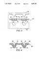
- FIG. 1is a partial sectional view of a composite structure used in fabrication of a flexible circuit at a first stage in fabrication
- FIG. 2Ais a partial sectional view of the composite structure at a second stage in fabrication
- FIG. 2Bis a plain view of the structure shown in FIG. 2A,
- FIG. 2Cis a bottom view of the structure shown in FIG. 2A.
- FIG. 3is a sectional view of the structure shown in FIGS. 2A-2C when received in a forming tool
- FIG. 4is a partial sectional view of the composite structure after forming in the tool shown in FIG. 3.
- FIG. 1illustrates a three-layer composite structure comprising a substrate 2 of insulating material having layers 4 and 6 of copper adhered to its front and back surfaces 8, 10 respectively.
- the substratemay, for example, be a single sheet of polyimide or it may be a composite sheet comprising two or more layers of polyimide bonded together by adhesive material.
- the insulating substrateis at least about 0.05 mm thick and the layers of copper are about 0.04 mm thick.
- layer 4is selectively etched to define discrete conductor runs 14 and contact pads 16.
- Layer 6is selectively etched to define discrete islands 18 and a ground plane 20. Islands 18 lie directly behind contact pads 14, so that each contact pad is confronted through the substrate by an island 18.
- the resulting structureis designated 22.
- the structure 22is placed in a forming tool comprising a female die 26 formed with recesses 30 shaped to correspond to the configuration of the desired contact bumps, and a male die 34 having pins 38 positioned to enter the recesses respectively.
- the composite structure 22is positioned with each contact pad 16 over one of the recesses 30, and the male die is then forced down, toward the female die.
- the pinsdeform the composite structure, so that the contact pads 16 form convex bumps 42 (FIG. 4) at the front surface of the substrate and the islands 18 define concave dimples 46 at the back surface of the substrate.
- a layer 48 of conductive material, such as silver paste,is applied to the back surface of the deformed structure 22' in order to provide a continuous ground plane. Such a layer is very flexible and does not interfere significantly with the ability of structure 22' to conform to a non-planar interface region of a module of electronic apparatus.
- the bumpsAfter the bumps have been formed, they are coated with an environmentally stable metal, such as gold (not shown), in order to ensure that a reliable electrically conductive pressure contact can be achieved between the bumps and the contact pads of a module of electronic apparatus.
- an environmentally stable metalsuch as gold (not shown)
- the flexible circuit board shown in FIG. 4has the advantage afforded by use of a layer of metal on the back surface of the substrate, without the disadvantage that arises from that layer being continuous.
- bumps having a height of from about 0.1 mm to about 0.3 mm, preferably about 0.2 mm,can be formed.
- the minimum spacing between the bumpsdepends on the thicknesses of the various layers of the flexible circuit board. In the case of the described embodiment of the invention, bumps have been formed with a spacing of about 1.8 mm.
- the inventionis not restricted to the particular embodiment that has been described, and that variations may be made therein without departing from the scope of the invention as defined in the appended claims and equivalents thereof.
- the inventionis not limited to use of copper as the metal of the contact pads and islands, since other formable metals, such as alloys of copper and alloys of iron, also could be used.
- the inventionis not restricted to the bumps being of any particular shape, since the shape of the bumps depends on the shape of the female die and the shape of the forming pin.
- the islands 18are shown as being of the same general shape as the contact pads 16, this is not essential, nor is it essential that the islands be the same size as the pads.
- a layer of flexible conductive materialbe applied to the back surface of the flexible circuit board after the bumps have been formed, this is not essential. It is also not essential to the invention that the forming tool have two rigid dies, since bumps may be formed by use of a male or female die in conjunction with a conformal forming member.
Landscapes
- Engineering & Computer Science (AREA)
- Manufacturing & Machinery (AREA)
- Microelectronics & Electronic Packaging (AREA)
- Manufacturing Of Electrical Connectors (AREA)
- Multi-Conductor Connections (AREA)
- Coupling Device And Connection With Printed Circuit (AREA)
- Printing Elements For Providing Electric Connections Between Printed Circuits (AREA)
Abstract
Description
Claims (12)
Priority Applications (2)
| Application Number | Priority Date | Filing Date | Title |
|---|---|---|---|
| US07/650,549US5097101A (en) | 1991-02-05 | 1991-02-05 | Method of forming a conductive contact bump on a flexible substrate and a flexible substrate |
| JP4054267AJPH05109457A (en) | 1991-02-05 | 1992-02-05 | Projection molding method |
Applications Claiming Priority (1)
| Application Number | Priority Date | Filing Date | Title |
|---|---|---|---|
| US07/650,549US5097101A (en) | 1991-02-05 | 1991-02-05 | Method of forming a conductive contact bump on a flexible substrate and a flexible substrate |
Publications (1)
| Publication Number | Publication Date |
|---|---|
| US5097101Atrue US5097101A (en) | 1992-03-17 |
Family
ID=24609368
Family Applications (1)
| Application Number | Title | Priority Date | Filing Date |
|---|---|---|---|
| US07/650,549Expired - LifetimeUS5097101A (en) | 1991-02-05 | 1991-02-05 | Method of forming a conductive contact bump on a flexible substrate and a flexible substrate |
Country Status (2)
| Country | Link |
|---|---|
| US (1) | US5097101A (en) |
| JP (1) | JPH05109457A (en) |
Cited By (53)
| Publication number | Priority date | Publication date | Assignee | Title |
|---|---|---|---|---|
| US5213511A (en)* | 1992-03-27 | 1993-05-25 | Hughes Aircraft Company | Dimple interconnect for flat cables and printed wiring boards |
| US5263244A (en)* | 1992-04-17 | 1993-11-23 | Gould Inc. | Method of making a flexible printed circuit sensor assembly for detecting optical pulses |
| US5283949A (en)* | 1992-11-03 | 1994-02-08 | Jurisich Peter L | Method of producing a printed circuit board having a conductive pattern thereon |
| US5288235A (en)* | 1992-12-14 | 1994-02-22 | Hughes Aircraft Company | Electrical interconnects having a supported bulge configuration |
| US5343616A (en)* | 1992-02-14 | 1994-09-06 | Rock Ltd. | Method of making high density self-aligning conductive networks and contact clusters |
| US5451722A (en)* | 1993-04-08 | 1995-09-19 | Gregoire; George D. | Printed circuit board with metallized grooves |
| GB2292840A (en)* | 1994-08-26 | 1996-03-06 | Nfi Electronics Ltd | Ensuring contact |
| US5528001A (en)* | 1992-02-14 | 1996-06-18 | Research Organization For Circuit Knowledge | Circuit of electrically conductive paths on a dielectric with a grid of isolated conductive features that are electrically insulated from the paths |
| US5584120A (en)* | 1992-02-14 | 1996-12-17 | Research Organization For Circuit Knowledge | Method of manufacturing printed circuits |
| US5629837A (en)* | 1995-09-20 | 1997-05-13 | Oz Technologies, Inc. | Button contact for surface mounting an IC device to a circuit board |
| US5928001A (en)* | 1997-09-08 | 1999-07-27 | Motorola, Inc. | Surface mountable flexible interconnect |
| US5950305A (en)* | 1992-02-14 | 1999-09-14 | Research Organization For Circuit Knowledge | Environmentally desirable method of manufacturing printed circuits |
| US6042391A (en)* | 1996-12-19 | 2000-03-28 | Telefonaktiebolaget Lm Ericsson | High density electrical connectors |
| US6085414A (en)* | 1996-08-15 | 2000-07-11 | Packard Hughes Interconnect Company | Method of making a flexible circuit with raised features protruding from two surfaces and products therefrom |
| US6256882B1 (en)* | 1998-07-14 | 2001-07-10 | Cascade Microtech, Inc. | Membrane probing system |
| US6407566B1 (en) | 2000-04-06 | 2002-06-18 | Micron Technology, Inc. | Test module for multi-chip module simulation testing of integrated circuit packages |
| US6437584B1 (en) | 1996-08-08 | 2002-08-20 | Cascade Microtech, Inc. | Membrane probing system with local contact scrub |
| US20020129894A1 (en)* | 2001-01-08 | 2002-09-19 | Kuo-Chuan Liu | Method for joining and an ultra-high density interconnect |
| US6464513B1 (en) | 2000-01-05 | 2002-10-15 | Micron Technology, Inc. | Adapter for non-permanently connecting integrated circuit devices to multi-chip modules and method of using same |
| US20030040139A1 (en)* | 2001-08-21 | 2003-02-27 | Canella Robert L. | Spring contact for establishing non-permanent electrical connection between an integrated circuit device lead element and a substrate, apparatus including same and method of use |
| US20030042595A1 (en)* | 2001-08-29 | 2003-03-06 | Canella Robert L. | Substrate with contact array and substrate assemblies |
| US20030090278A1 (en)* | 2001-08-21 | 2003-05-15 | Kenneth Smith | Membrane probing system |
| US6578264B1 (en) | 1999-06-04 | 2003-06-17 | Cascade Microtech, Inc. | Method for constructing a membrane probe using a depression |
| US20030132767A1 (en)* | 2000-02-25 | 2003-07-17 | Tervo Paul A. | Membrane probing system |
| US20040000371A1 (en)* | 1999-11-03 | 2004-01-01 | Bhullar Raghbir S. | Embedded metallic deposits |
| US20040088854A1 (en)* | 2001-11-28 | 2004-05-13 | 3M Innovative Properties Company | Abrasion resistant electrode and device |
| US20050237364A1 (en)* | 2004-04-26 | 2005-10-27 | Hirosumi Ito | Printed wiring board and electric device using the same |
| US20060006889A1 (en)* | 2004-07-07 | 2006-01-12 | Kenneth Smith | Probe head having a membrane suspended probe |
| US7161363B2 (en) | 2002-05-23 | 2007-01-09 | Cascade Microtech, Inc. | Probe for testing a device under test |
| US7233160B2 (en) | 2000-12-04 | 2007-06-19 | Cascade Microtech, Inc. | Wafer probe |
| US7271603B2 (en) | 2003-05-23 | 2007-09-18 | Cascade Microtech, Inc. | Shielded probe for testing a device under test |
| US7285969B2 (en) | 2002-11-13 | 2007-10-23 | Cascade Microtech, Inc. | Probe for combined signals |
| US7403028B2 (en) | 2006-06-12 | 2008-07-22 | Cascade Microtech, Inc. | Test structure and probe for differential signals |
| US7420381B2 (en) | 2004-09-13 | 2008-09-02 | Cascade Microtech, Inc. | Double sided probing structures |
| US7427868B2 (en) | 2003-12-24 | 2008-09-23 | Cascade Microtech, Inc. | Active wafer probe |
| EP1973158A1 (en) | 2007-03-23 | 2008-09-24 | Delphi Technologies, Inc. | Electronic component |
| US7443186B2 (en) | 2006-06-12 | 2008-10-28 | Cascade Microtech, Inc. | On-wafer test structures for differential signals |
| US7449899B2 (en) | 2005-06-08 | 2008-11-11 | Cascade Microtech, Inc. | Probe for high frequency signals |
| US7504842B2 (en) | 1997-05-28 | 2009-03-17 | Cascade Microtech, Inc. | Probe holder for testing of a test device |
| US7535247B2 (en) | 2005-01-31 | 2009-05-19 | Cascade Microtech, Inc. | Interface for testing semiconductors |
| US7609077B2 (en) | 2006-06-09 | 2009-10-27 | Cascade Microtech, Inc. | Differential signal probe with integral balun |
| US7619419B2 (en) | 2005-06-13 | 2009-11-17 | Cascade Microtech, Inc. | Wideband active-passive differential signal probe |
| US7656172B2 (en) | 2005-01-31 | 2010-02-02 | Cascade Microtech, Inc. | System for testing semiconductors |
| US7723999B2 (en) | 2006-06-12 | 2010-05-25 | Cascade Microtech, Inc. | Calibration structures for differential signal probing |
| US7764072B2 (en) | 2006-06-12 | 2010-07-27 | Cascade Microtech, Inc. | Differential signal probing system |
| US7876114B2 (en) | 2007-08-08 | 2011-01-25 | Cascade Microtech, Inc. | Differential waveguide probe |
| US7888957B2 (en) | 2008-10-06 | 2011-02-15 | Cascade Microtech, Inc. | Probing apparatus with impedance optimized interface |
| US20110113619A1 (en)* | 2009-11-17 | 2011-05-19 | Viscarra Alberto F | Process for fabricating a three dimensional molded feed structure |
| US8410806B2 (en) | 2008-11-21 | 2013-04-02 | Cascade Microtech, Inc. | Replaceable coupon for a probing apparatus |
| US9491854B2 (en) | 2009-07-31 | 2016-11-08 | Raytheon Company | Multi-layer microwave corrugated printed circuit board and method |
| WO2018231442A1 (en)* | 2017-06-12 | 2018-12-20 | Invensas Corporation | Deformable electrical contacts with conformable target pads |
| CN112040671A (en)* | 2020-08-30 | 2020-12-04 | 深圳市实锐泰科技有限公司 | Manufacturing method of flexible board raised circuit structure and flexible board raised circuit structure |
| EP4326011A3 (en)* | 2022-08-17 | 2024-02-28 | Aptiv Technologies Limited | Systems and methods for shaping flexible circuits to improve routing and attachment |
Families Citing this family (2)
| Publication number | Priority date | Publication date | Assignee | Title |
|---|---|---|---|---|
| JP4723431B2 (en)* | 2006-07-28 | 2011-07-13 | シャープ株式会社 | Circuit board manufacturing method |
| JP5363943B2 (en)* | 2009-10-26 | 2013-12-11 | 株式会社日本マイクロニクス | Conductive sheet, method for manufacturing conductive sheet, probe card, and inspection apparatus |
Citations (9)
| Publication number | Priority date | Publication date | Assignee | Title |
|---|---|---|---|---|
| US2912745A (en)* | 1955-08-25 | 1959-11-17 | Erie Resistor Corp | Method of making a printed circuit |
| US4116517A (en)* | 1976-04-15 | 1978-09-26 | International Telephone And Telegraph Corporation | Flexible printed circuit and electrical connection therefor |
| US4173712A (en)* | 1978-08-30 | 1979-11-06 | General Ionex Corporation | Electrical circuit component protecting device |
| US4396457A (en)* | 1982-03-17 | 1983-08-02 | E. I. Du Pont De Nemours And Company | Method of making bumped-beam tape |
| US4403272A (en)* | 1980-06-02 | 1983-09-06 | Oak Industries Inc. | Membrane switch interconnect tail and printed circuit board connection |
| US4736277A (en)* | 1986-01-03 | 1988-04-05 | Motorola, Inc. | Metal printed circuit panels including mesas for coupling circuitry thereon to signal ground |
| US4784972A (en)* | 1984-08-18 | 1988-11-15 | Matsushita Electric Industrial Co. Ltd. | Method of joining beam leads with projections to device electrodes |
| US4835859A (en)* | 1987-12-03 | 1989-06-06 | Tektronix, Inc. | Method of forming a contact bump |
| GB2222727A (en)* | 1988-08-31 | 1990-03-14 | Shinetsu Polymer Co | Method for preparing a double-sided flexible circuit board with electrical connection at a through-hole |
- 1991
- 1991-02-05USUS07/650,549patent/US5097101A/ennot_activeExpired - Lifetime
- 1992
- 1992-02-05JPJP4054267Apatent/JPH05109457A/enactivePending
Patent Citations (9)
| Publication number | Priority date | Publication date | Assignee | Title |
|---|---|---|---|---|
| US2912745A (en)* | 1955-08-25 | 1959-11-17 | Erie Resistor Corp | Method of making a printed circuit |
| US4116517A (en)* | 1976-04-15 | 1978-09-26 | International Telephone And Telegraph Corporation | Flexible printed circuit and electrical connection therefor |
| US4173712A (en)* | 1978-08-30 | 1979-11-06 | General Ionex Corporation | Electrical circuit component protecting device |
| US4403272A (en)* | 1980-06-02 | 1983-09-06 | Oak Industries Inc. | Membrane switch interconnect tail and printed circuit board connection |
| US4396457A (en)* | 1982-03-17 | 1983-08-02 | E. I. Du Pont De Nemours And Company | Method of making bumped-beam tape |
| US4784972A (en)* | 1984-08-18 | 1988-11-15 | Matsushita Electric Industrial Co. Ltd. | Method of joining beam leads with projections to device electrodes |
| US4736277A (en)* | 1986-01-03 | 1988-04-05 | Motorola, Inc. | Metal printed circuit panels including mesas for coupling circuitry thereon to signal ground |
| US4835859A (en)* | 1987-12-03 | 1989-06-06 | Tektronix, Inc. | Method of forming a contact bump |
| GB2222727A (en)* | 1988-08-31 | 1990-03-14 | Shinetsu Polymer Co | Method for preparing a double-sided flexible circuit board with electrical connection at a through-hole |
Cited By (130)
| Publication number | Priority date | Publication date | Assignee | Title |
|---|---|---|---|---|
| US5477612A (en)* | 1992-02-14 | 1995-12-26 | Rock Ltd. Partnership | Method of making high density conductive networks |
| US5950305A (en)* | 1992-02-14 | 1999-09-14 | Research Organization For Circuit Knowledge | Environmentally desirable method of manufacturing printed circuits |
| US5819579A (en)* | 1992-02-14 | 1998-10-13 | Research Organization For Circuit Knowledge | Forming die for manufacturing printed circuits |
| US5584120A (en)* | 1992-02-14 | 1996-12-17 | Research Organization For Circuit Knowledge | Method of manufacturing printed circuits |
| US5343616A (en)* | 1992-02-14 | 1994-09-06 | Rock Ltd. | Method of making high density self-aligning conductive networks and contact clusters |
| US5526565A (en)* | 1992-02-14 | 1996-06-18 | Research Organization For Circuit Knowledge Limited Partnership | High density self-aligning conductive networks and contact clusters and method and apparatus for making same |
| US5528001A (en)* | 1992-02-14 | 1996-06-18 | Research Organization For Circuit Knowledge | Circuit of electrically conductive paths on a dielectric with a grid of isolated conductive features that are electrically insulated from the paths |
| US5213511A (en)* | 1992-03-27 | 1993-05-25 | Hughes Aircraft Company | Dimple interconnect for flat cables and printed wiring boards |
| US5263244A (en)* | 1992-04-17 | 1993-11-23 | Gould Inc. | Method of making a flexible printed circuit sensor assembly for detecting optical pulses |
| US5390670A (en)* | 1992-04-17 | 1995-02-21 | Gould Electronics Inc. | Flexible printed circuit sensor assembly for detecting optical pulses |
| US5283949A (en)* | 1992-11-03 | 1994-02-08 | Jurisich Peter L | Method of producing a printed circuit board having a conductive pattern thereon |
| US5288235A (en)* | 1992-12-14 | 1994-02-22 | Hughes Aircraft Company | Electrical interconnects having a supported bulge configuration |
| US5451722A (en)* | 1993-04-08 | 1995-09-19 | Gregoire; George D. | Printed circuit board with metallized grooves |
| GB2292840A (en)* | 1994-08-26 | 1996-03-06 | Nfi Electronics Ltd | Ensuring contact |
| WO1996019912A1 (en)* | 1994-12-19 | 1996-06-27 | Research Organization For Circuit Knowledge | An environmentally desirable method of manufacturing printed circuits, printed circuits made thereby and associated apparatus |
| US5629837A (en)* | 1995-09-20 | 1997-05-13 | Oz Technologies, Inc. | Button contact for surface mounting an IC device to a circuit board |
| US6437584B1 (en) | 1996-08-08 | 2002-08-20 | Cascade Microtech, Inc. | Membrane probing system with local contact scrub |
| US6927585B2 (en) | 1996-08-08 | 2005-08-09 | Cascade Microtech, Inc. | Membrane probing system with local contact scrub |
| US20050231223A1 (en)* | 1996-08-08 | 2005-10-20 | Cascade Microtech, Inc. | Membrane probing system with local contact scrub |
| US7541821B2 (en) | 1996-08-08 | 2009-06-02 | Cascade Microtech, Inc. | Membrane probing system with local contact scrub |
| US7893704B2 (en) | 1996-08-08 | 2011-02-22 | Cascade Microtech, Inc. | Membrane probing structure with laterally scrubbing contacts |
| US20020135388A1 (en)* | 1996-08-08 | 2002-09-26 | Gleason K. Reed | Membrane probing system with local contact scrub |
| US7109731B2 (en) | 1996-08-08 | 2006-09-19 | Cascade Microtech, Inc. | Membrane probing system with local contact scrub |
| US6085414A (en)* | 1996-08-15 | 2000-07-11 | Packard Hughes Interconnect Company | Method of making a flexible circuit with raised features protruding from two surfaces and products therefrom |
| US6042391A (en)* | 1996-12-19 | 2000-03-28 | Telefonaktiebolaget Lm Ericsson | High density electrical connectors |
| US7504842B2 (en) | 1997-05-28 | 2009-03-17 | Cascade Microtech, Inc. | Probe holder for testing of a test device |
| US5928001A (en)* | 1997-09-08 | 1999-07-27 | Motorola, Inc. | Surface mountable flexible interconnect |
| US6860009B2 (en) | 1998-07-14 | 2005-03-01 | Cascade Microtech, Inc. | Probe construction using a recess |
| US7681312B2 (en) | 1998-07-14 | 2010-03-23 | Cascade Microtech, Inc. | Membrane probing system |
| US7400155B2 (en) | 1998-07-14 | 2008-07-15 | Cascade Microtech, Inc. | Membrane probing system |
| US7266889B2 (en) | 1998-07-14 | 2007-09-11 | Cascade Microtech, Inc. | Membrane probing system |
| US7761986B2 (en) | 1998-07-14 | 2010-07-27 | Cascade Microtech, Inc. | Membrane probing method using improved contact |
| US8451017B2 (en) | 1998-07-14 | 2013-05-28 | Cascade Microtech, Inc. | Membrane probing method using improved contact |
| US6708386B2 (en) | 1998-07-14 | 2004-03-23 | Cascade Microtech, Inc. | Method for probing an electrical device having a layer of oxide thereon |
| US6256882B1 (en)* | 1998-07-14 | 2001-07-10 | Cascade Microtech, Inc. | Membrane probing system |
| US20050136562A1 (en)* | 1998-07-14 | 2005-06-23 | Reed Gleason | Membrane probing system |
| US20040093716A1 (en)* | 1998-07-14 | 2004-05-20 | Reed Gleason | Membrane probing system |
| US20040154155A1 (en)* | 1998-07-14 | 2004-08-12 | Reed Gleason | Membrane probing system |
| US6825677B2 (en) | 1998-07-14 | 2004-11-30 | Cascade Microtech, Inc. | Membrane probing system |
| US7533462B2 (en) | 1999-06-04 | 2009-05-19 | Cascade Microtech, Inc. | Method of constructing a membrane probe |
| US6578264B1 (en) | 1999-06-04 | 2003-06-17 | Cascade Microtech, Inc. | Method for constructing a membrane probe using a depression |
| US7178236B2 (en) | 1999-06-04 | 2007-02-20 | Cascade Microtech, Inc. | Method for constructing a membrane probe using a depression |
| US20030192183A1 (en)* | 1999-06-04 | 2003-10-16 | Reed Gleason | Method for constructing a membrane probe using a depression |
| US20040000371A1 (en)* | 1999-11-03 | 2004-01-01 | Bhullar Raghbir S. | Embedded metallic deposits |
| US7326066B2 (en) | 2000-01-05 | 2008-02-05 | Micron Technology, Inc. | Adapter for non-permanently connecting integrated circuit devices to multi-chip modules and method of using same |
| US20050082661A1 (en)* | 2000-01-05 | 2005-04-21 | Saeed Momempour | Adapter for non-permanently connecting integrated circuit devices to multi-chip modules and method of using same |
| US20020196598A1 (en)* | 2000-01-05 | 2002-12-26 | Saeed Momenpour | Adapter for non-permanently connecting integrated circuit devices to multi-chip modules and method of using same |
| US6464513B1 (en) | 2000-01-05 | 2002-10-15 | Micron Technology, Inc. | Adapter for non-permanently connecting integrated circuit devices to multi-chip modules and method of using same |
| US6843661B2 (en) | 2000-01-05 | 2005-01-18 | Micron Technology, Inc. | Adapter for non-permanently connecting integrated circuit devices to multi-chip modules and method of using same |
| US7403025B2 (en) | 2000-02-25 | 2008-07-22 | Cascade Microtech, Inc. | Membrane probing system |
| US20050007131A1 (en)* | 2000-02-25 | 2005-01-13 | Cascade Microtech, Inc. | Membrane probing system |
| US6930498B2 (en) | 2000-02-25 | 2005-08-16 | Cascade Microtech, Inc. | Membrane probing system |
| US6838890B2 (en) | 2000-02-25 | 2005-01-04 | Cascade Microtech, Inc. | Membrane probing system |
| US20050248359A1 (en)* | 2000-02-25 | 2005-11-10 | Cascade Microtech, Inc. | Membrane probing system |
| US20030132767A1 (en)* | 2000-02-25 | 2003-07-17 | Tervo Paul A. | Membrane probing system |
| US7148711B2 (en) | 2000-02-25 | 2006-12-12 | Cascade Microtech, Inc. | Membrane probing system |
| US6407566B1 (en) | 2000-04-06 | 2002-06-18 | Micron Technology, Inc. | Test module for multi-chip module simulation testing of integrated circuit packages |
| US7688097B2 (en) | 2000-12-04 | 2010-03-30 | Cascade Microtech, Inc. | Wafer probe |
| US7233160B2 (en) | 2000-12-04 | 2007-06-19 | Cascade Microtech, Inc. | Wafer probe |
| US7456646B2 (en) | 2000-12-04 | 2008-11-25 | Cascade Microtech, Inc. | Wafer probe |
| US7495461B2 (en) | 2000-12-04 | 2009-02-24 | Cascade Microtech, Inc. | Wafer probe |
| US7761983B2 (en) | 2000-12-04 | 2010-07-27 | Cascade Microtech, Inc. | Method of assembling a wafer probe |
| US6884313B2 (en) | 2001-01-08 | 2005-04-26 | Fujitsu Limited | Method and system for joining and an ultra-high density interconnect |
| US20020129894A1 (en)* | 2001-01-08 | 2002-09-19 | Kuo-Chuan Liu | Method for joining and an ultra-high density interconnect |
| US7355420B2 (en) | 2001-08-21 | 2008-04-08 | Cascade Microtech, Inc. | Membrane probing system |
| US20030090278A1 (en)* | 2001-08-21 | 2003-05-15 | Kenneth Smith | Membrane probing system |
| US7045889B2 (en) | 2001-08-21 | 2006-05-16 | Micron Technology, Inc. | Device for establishing non-permanent electrical connection between an integrated circuit device lead element and a substrate |
| US20050067687A1 (en)* | 2001-08-21 | 2005-03-31 | Canella Robert L. | Device for establishing non-permanent electrical connection between an integrated circuit device lead element and a substrate |
| US7279788B2 (en) | 2001-08-21 | 2007-10-09 | Micron Technology, Inc. | Device for establishing non-permanent electrical connection between an integrated circuit device lead element and a substrate |
| US7492175B2 (en) | 2001-08-21 | 2009-02-17 | Cascade Microtech, Inc. | Membrane probing system |
| US7192806B2 (en) | 2001-08-21 | 2007-03-20 | Micron Technology, Inc. | Method of establishing non-permanent electrical connection between an integrated circuit device lead element and a substrate |
| US20030040139A1 (en)* | 2001-08-21 | 2003-02-27 | Canella Robert L. | Spring contact for establishing non-permanent electrical connection between an integrated circuit device lead element and a substrate, apparatus including same and method of use |
| US7094065B2 (en) | 2001-08-21 | 2006-08-22 | Micron Technology, Inc. | Device for establishing non-permanent electrical connection between an integrated circuit device lead element and a substrate |
| US20050070133A1 (en)* | 2001-08-21 | 2005-03-31 | Canella Robert L. | Device for establishing non-permanent electrical connection between an integrated circuit device lead element and a substrate |
| US20050073041A1 (en)* | 2001-08-21 | 2005-04-07 | Canella Robert L. | Device for establishing non-permanent electrical connection between an integrated circuit device lead element and a substrate |
| US7049693B2 (en) | 2001-08-29 | 2006-05-23 | Micron Technology, Inc. | Electrical contact array for substrate assemblies |
| US20030042595A1 (en)* | 2001-08-29 | 2003-03-06 | Canella Robert L. | Substrate with contact array and substrate assemblies |
| US7120999B2 (en) | 2001-08-29 | 2006-10-17 | Micron Technology, Inc. | Methods of forming a contact array in situ on a substrate |
| US20040058470A1 (en)* | 2001-08-29 | 2004-03-25 | Canella Robert L. | Methods of forming a contact array in situ on a substrate and resulting substrate assemblies |
| US20040088854A1 (en)* | 2001-11-28 | 2004-05-13 | 3M Innovative Properties Company | Abrasion resistant electrode and device |
| US7069651B2 (en)* | 2001-11-28 | 2006-07-04 | 3M Innovative Properties Company | Abrasion resistant electrode and device |
| US7489149B2 (en) | 2002-05-23 | 2009-02-10 | Cascade Microtech, Inc. | Shielded probe for testing a device under test |
| US7518387B2 (en) | 2002-05-23 | 2009-04-14 | Cascade Microtech, Inc. | Shielded probe for testing a device under test |
| US7304488B2 (en) | 2002-05-23 | 2007-12-04 | Cascade Microtech, Inc. | Shielded probe for high-frequency testing of a device under test |
| US7436194B2 (en) | 2002-05-23 | 2008-10-14 | Cascade Microtech, Inc. | Shielded probe with low contact resistance for testing a device under test |
| US7161363B2 (en) | 2002-05-23 | 2007-01-09 | Cascade Microtech, Inc. | Probe for testing a device under test |
| US7482823B2 (en) | 2002-05-23 | 2009-01-27 | Cascade Microtech, Inc. | Shielded probe for testing a device under test |
| US7453276B2 (en) | 2002-11-13 | 2008-11-18 | Cascade Microtech, Inc. | Probe for combined signals |
| US7285969B2 (en) | 2002-11-13 | 2007-10-23 | Cascade Microtech, Inc. | Probe for combined signals |
| US7417446B2 (en) | 2002-11-13 | 2008-08-26 | Cascade Microtech, Inc. | Probe for combined signals |
| US7498829B2 (en) | 2003-05-23 | 2009-03-03 | Cascade Microtech, Inc. | Shielded probe for testing a device under test |
| US7501842B2 (en) | 2003-05-23 | 2009-03-10 | Cascade Microtech, Inc. | Shielded probe for testing a device under test |
| US7271603B2 (en) | 2003-05-23 | 2007-09-18 | Cascade Microtech, Inc. | Shielded probe for testing a device under test |
| US7898273B2 (en) | 2003-05-23 | 2011-03-01 | Cascade Microtech, Inc. | Probe for testing a device under test |
| US7427868B2 (en) | 2003-12-24 | 2008-09-23 | Cascade Microtech, Inc. | Active wafer probe |
| US7759953B2 (en) | 2003-12-24 | 2010-07-20 | Cascade Microtech, Inc. | Active wafer probe |
| US7703889B2 (en) | 2004-04-26 | 2010-04-27 | Brother Kogyo Kabushiki Kaisha | Printed wiring board and electric device using the same |
| US20050237364A1 (en)* | 2004-04-26 | 2005-10-27 | Hirosumi Ito | Printed wiring board and electric device using the same |
| US7514944B2 (en) | 2004-07-07 | 2009-04-07 | Cascade Microtech, Inc. | Probe head having a membrane suspended probe |
| US7368927B2 (en) | 2004-07-07 | 2008-05-06 | Cascade Microtech, Inc. | Probe head having a membrane suspended probe |
| US20060006889A1 (en)* | 2004-07-07 | 2006-01-12 | Kenneth Smith | Probe head having a membrane suspended probe |
| US7420381B2 (en) | 2004-09-13 | 2008-09-02 | Cascade Microtech, Inc. | Double sided probing structures |
| US8013623B2 (en) | 2004-09-13 | 2011-09-06 | Cascade Microtech, Inc. | Double sided probing structures |
| US7656172B2 (en) | 2005-01-31 | 2010-02-02 | Cascade Microtech, Inc. | System for testing semiconductors |
| US7940069B2 (en) | 2005-01-31 | 2011-05-10 | Cascade Microtech, Inc. | System for testing semiconductors |
| US7898281B2 (en) | 2005-01-31 | 2011-03-01 | Cascade Mircotech, Inc. | Interface for testing semiconductors |
| US7535247B2 (en) | 2005-01-31 | 2009-05-19 | Cascade Microtech, Inc. | Interface for testing semiconductors |
| US7449899B2 (en) | 2005-06-08 | 2008-11-11 | Cascade Microtech, Inc. | Probe for high frequency signals |
| US7619419B2 (en) | 2005-06-13 | 2009-11-17 | Cascade Microtech, Inc. | Wideband active-passive differential signal probe |
| US7609077B2 (en) | 2006-06-09 | 2009-10-27 | Cascade Microtech, Inc. | Differential signal probe with integral balun |
| US7764072B2 (en) | 2006-06-12 | 2010-07-27 | Cascade Microtech, Inc. | Differential signal probing system |
| US7750652B2 (en) | 2006-06-12 | 2010-07-06 | Cascade Microtech, Inc. | Test structure and probe for differential signals |
| US7723999B2 (en) | 2006-06-12 | 2010-05-25 | Cascade Microtech, Inc. | Calibration structures for differential signal probing |
| US7403028B2 (en) | 2006-06-12 | 2008-07-22 | Cascade Microtech, Inc. | Test structure and probe for differential signals |
| US7443186B2 (en) | 2006-06-12 | 2008-10-28 | Cascade Microtech, Inc. | On-wafer test structures for differential signals |
| EP1973158A1 (en) | 2007-03-23 | 2008-09-24 | Delphi Technologies, Inc. | Electronic component |
| US7876114B2 (en) | 2007-08-08 | 2011-01-25 | Cascade Microtech, Inc. | Differential waveguide probe |
| US7888957B2 (en) | 2008-10-06 | 2011-02-15 | Cascade Microtech, Inc. | Probing apparatus with impedance optimized interface |
| US10267848B2 (en) | 2008-11-21 | 2019-04-23 | Formfactor Beaverton, Inc. | Method of electrically contacting a bond pad of a device under test with a probe |
| US8410806B2 (en) | 2008-11-21 | 2013-04-02 | Cascade Microtech, Inc. | Replaceable coupon for a probing apparatus |
| US9429638B2 (en) | 2008-11-21 | 2016-08-30 | Cascade Microtech, Inc. | Method of replacing an existing contact of a wafer probing assembly |
| US9491854B2 (en) | 2009-07-31 | 2016-11-08 | Raytheon Company | Multi-layer microwave corrugated printed circuit board and method |
| US9072164B2 (en)* | 2009-11-17 | 2015-06-30 | Raytheon Company | Process for fabricating a three dimensional molded feed structure |
| US20110113619A1 (en)* | 2009-11-17 | 2011-05-19 | Viscarra Alberto F | Process for fabricating a three dimensional molded feed structure |
| WO2018231442A1 (en)* | 2017-06-12 | 2018-12-20 | Invensas Corporation | Deformable electrical contacts with conformable target pads |
| US10750614B2 (en)* | 2017-06-12 | 2020-08-18 | Invensas Corporation | Deformable electrical contacts with conformable target pads |
| CN112040671A (en)* | 2020-08-30 | 2020-12-04 | 深圳市实锐泰科技有限公司 | Manufacturing method of flexible board raised circuit structure and flexible board raised circuit structure |
| CN112040671B (en)* | 2020-08-30 | 2024-03-15 | 深圳市实锐泰科技有限公司 | Manufacturing method of flexible board raised circuit structure and flexible board raised circuit structure |
| EP4326011A3 (en)* | 2022-08-17 | 2024-02-28 | Aptiv Technologies Limited | Systems and methods for shaping flexible circuits to improve routing and attachment |
| US12156342B2 (en) | 2022-08-17 | 2024-11-26 | Aptiv Technologies AG | Systems and methods for shaping flexible circuits to improve routing and attachment |
Also Published As
| Publication number | Publication date |
|---|---|
| JPH05109457A (en) | 1993-04-30 |
Similar Documents
| Publication | Publication Date | Title |
|---|---|---|
| US5097101A (en) | Method of forming a conductive contact bump on a flexible substrate and a flexible substrate | |
| KR100437436B1 (en) | Semiconductor package manufacturing method and semiconductor package | |
| US6313402B1 (en) | Stress relief bend useful in an integrated circuit redistribution patch | |
| US6420664B1 (en) | Metal foil having bumps, circuit substrate having the metal foil, and semiconductor device having the circuit substrate | |
| JP2934202B2 (en) | Method for forming conductive bumps on wiring board | |
| US5329423A (en) | Compressive bump-and-socket interconnection scheme for integrated circuits | |
| JP2867209B2 (en) | Method of connecting flexible circuit board to contact object and structure thereof | |
| JPH0992776A (en) | Lead frame and semiconductor device | |
| US20040201396A1 (en) | Floating interposer | |
| US6989291B2 (en) | Method for manufacturing circuit devices | |
| US6271057B1 (en) | Method of making semiconductor chip package | |
| US7030033B2 (en) | Method for manufacturing circuit devices | |
| US20040101666A1 (en) | Inspection contact sheet and method of fabricating the same | |
| JPH07335695A (en) | IC chip module assembly and biasing member used for the same | |
| US4835859A (en) | Method of forming a contact bump | |
| US6802930B2 (en) | Method of making a laminated structure | |
| JPH1013003A (en) | Semiconductor device | |
| DE102015114645B4 (en) | SMART CARD, DEVICE AND METHOD | |
| US12124035B2 (en) | Stretchable film assembly with conductive traces | |
| JPH09148378A (en) | IC module for IC card, manufacturing method thereof, and IC card using the IC module | |
| US6109369A (en) | Chip scale package | |
| JP4030220B2 (en) | Semiconductor chip mounting structure | |
| JP2823667B2 (en) | Semiconductor element mounting method | |
| TWI288970B (en) | Method of making reinforced semiconductor package | |
| JPH1065322A (en) | Method for forming conductive bumps on electrical components |
Legal Events
| Date | Code | Title | Description |
|---|---|---|---|
| AS | Assignment | Owner name:TEKTRONIX, INC. AN OR CORPORATION, OREGON Free format text:ASSIGNMENT OF ASSIGNORS INTEREST.;ASSIGNOR:TROBOUGH, DOUGLAS W.;REEL/FRAME:005935/0992 Effective date:19910201 | |
| STCF | Information on status: patent grant | Free format text:PATENTED CASE | |
| FPAY | Fee payment | Year of fee payment:4 | |
| FPAY | Fee payment | Year of fee payment:8 | |
| AS | Assignment | Owner name:LAURENCE J. MARHOEFER, VIRGINIA Free format text:ASSIGNMENT OF ASSIGNORS INTEREST;ASSIGNOR:TEKTONIX, INC.;REEL/FRAME:011035/0920 Effective date:20000622 | |
| AS | Assignment | Owner name:RESTON POINTE LLC, MICHIGAN Free format text:ASSIGNMENT OF ASSIGNORS INTEREST;ASSIGNOR:MARHOEFER, LAURENCE J.;REEL/FRAME:012188/0900 Effective date:20000926 | |
| FEPP | Fee payment procedure | Free format text:PAYOR NUMBER ASSIGNED (ORIGINAL EVENT CODE: ASPN); ENTITY STATUS OF PATENT OWNER: LARGE ENTITY | |
| AS | Assignment | Owner name:RESEARCH INVESTMENT NETWORK, INC., CALIFORNIA Free format text:ASSIGNMENT OF ASSIGNORS INTEREST;ASSIGNOR:RESTON POINTE, LLC;REEL/FRAME:013634/0765 Effective date:20030502 | |
| FPAY | Fee payment | Year of fee payment:12 | |
| AS | Assignment | Owner name:AMERICAN VIDEO GRAPHICS, L.P., TEXAS Free format text:ASSIGNMENT OF ASSIGNORS INTEREST;ASSIGNOR:RESEARCH INVESTMENT NETWORK, INC.;REEL/FRAME:014734/0229 Effective date:20040614 |