US5088190A - Method of forming an apparatus for burn in testing of integrated circuit chip - Google Patents
Method of forming an apparatus for burn in testing of integrated circuit chipDownload PDFInfo
- Publication number
- US5088190A US5088190AUS07/575,456US57545690AUS5088190AUS 5088190 AUS5088190 AUS 5088190AUS 57545690 AUS57545690 AUS 57545690AUS 5088190 AUS5088190 AUS 5088190A
- Authority
- US
- United States
- Prior art keywords
- integrated circuit
- chip
- circuit chip
- socket
- connection
- Prior art date
- Legal status (The legal status is an assumption and is not a legal conclusion. Google has not performed a legal analysis and makes no representation as to the accuracy of the status listed.)
- Expired - Lifetime
Links
Images

Classifications
- G—PHYSICS
- G01—MEASURING; TESTING
- G01R—MEASURING ELECTRIC VARIABLES; MEASURING MAGNETIC VARIABLES
- G01R31/00—Arrangements for testing electric properties; Arrangements for locating electric faults; Arrangements for electrical testing characterised by what is being tested not provided for elsewhere
- G01R31/28—Testing of electronic circuits, e.g. by signal tracer
- G01R31/2851—Testing of integrated circuits [IC]
- G01R31/2855—Environmental, reliability or burn-in testing
- G01R31/286—External aspects, e.g. related to chambers, contacting devices or handlers
- G01R31/2863—Contacting devices, e.g. sockets, burn-in boards or mounting fixtures
- G—PHYSICS
- G01—MEASURING; TESTING
- G01R—MEASURING ELECTRIC VARIABLES; MEASURING MAGNETIC VARIABLES
- G01R1/00—Details of instruments or arrangements of the types included in groups G01R5/00 - G01R13/00 and G01R31/00
- G01R1/02—General constructional details
- G01R1/04—Housings; Supporting members; Arrangements of terminals
- G01R1/0408—Test fixtures or contact fields; Connectors or connecting adaptors; Test clips; Test sockets
- G01R1/0433—Sockets for IC's or transistors
- G01R1/0483—Sockets for un-leaded IC's having matrix type contact fields, e.g. BGA or PGA devices; Sockets for unpackaged, naked chips
- G—PHYSICS
- G01—MEASURING; TESTING
- G01R—MEASURING ELECTRIC VARIABLES; MEASURING MAGNETIC VARIABLES
- G01R31/00—Arrangements for testing electric properties; Arrangements for locating electric faults; Arrangements for electrical testing characterised by what is being tested not provided for elsewhere
- G01R31/28—Testing of electronic circuits, e.g. by signal tracer
- G01R31/2851—Testing of integrated circuits [IC]
- G01R31/2886—Features relating to contacting the IC under test, e.g. probe heads; chucks
- H—ELECTRICITY
- H01—ELECTRIC ELEMENTS
- H01R—ELECTRICALLY-CONDUCTIVE CONNECTIONS; STRUCTURAL ASSOCIATIONS OF A PLURALITY OF MUTUALLY-INSULATED ELECTRICAL CONNECTING ELEMENTS; COUPLING DEVICES; CURRENT COLLECTORS
- H01R12/00—Structural associations of a plurality of mutually-insulated electrical connecting elements, specially adapted for printed circuits, e.g. printed circuit boards [PCB], flat or ribbon cables, or like generally planar structures, e.g. terminal strips, terminal blocks; Coupling devices specially adapted for printed circuits, flat or ribbon cables, or like generally planar structures; Terminals specially adapted for contact with, or insertion into, printed circuits, flat or ribbon cables, or like generally planar structures
- H01R12/50—Fixed connections
- H01R12/51—Fixed connections for rigid printed circuits or like structures
- H01R12/55—Fixed connections for rigid printed circuits or like structures characterised by the terminals
- H01R12/57—Fixed connections for rigid printed circuits or like structures characterised by the terminals surface mounting terminals
- H—ELECTRICITY
- H01—ELECTRIC ELEMENTS
- H01L—SEMICONDUCTOR DEVICES NOT COVERED BY CLASS H10
- H01L2224/00—Indexing scheme for arrangements for connecting or disconnecting semiconductor or solid-state bodies and methods related thereto as covered by H01L24/00
- H01L2224/01—Means for bonding being attached to, or being formed on, the surface to be connected, e.g. chip-to-package, die-attach, "first-level" interconnects; Manufacturing methods related thereto
- H01L2224/42—Wire connectors; Manufacturing methods related thereto
- H01L2224/47—Structure, shape, material or disposition of the wire connectors after the connecting process
- H01L2224/48—Structure, shape, material or disposition of the wire connectors after the connecting process of an individual wire connector
- H01L2224/4805—Shape
- H01L2224/4809—Loop shape
- H01L2224/48091—Arched
- H—ELECTRICITY
- H01—ELECTRIC ELEMENTS
- H01L—SEMICONDUCTOR DEVICES NOT COVERED BY CLASS H10
- H01L2924/00—Indexing scheme for arrangements or methods for connecting or disconnecting semiconductor or solid-state bodies as covered by H01L24/00
- H01L2924/01—Chemical elements
- H01L2924/01014—Silicon [Si]
- H—ELECTRICITY
- H01—ELECTRIC ELEMENTS
- H01L—SEMICONDUCTOR DEVICES NOT COVERED BY CLASS H10
- H01L2924/00—Indexing scheme for arrangements or methods for connecting or disconnecting semiconductor or solid-state bodies as covered by H01L24/00
- H01L2924/01—Chemical elements
- H01L2924/01039—Yttrium [Y]
- H—ELECTRICITY
- H01—ELECTRIC ELEMENTS
- H01L—SEMICONDUCTOR DEVICES NOT COVERED BY CLASS H10
- H01L2924/00—Indexing scheme for arrangements or methods for connecting or disconnecting semiconductor or solid-state bodies as covered by H01L24/00
- H01L2924/01—Chemical elements
- H01L2924/01079—Gold [Au]
- H—ELECTRICITY
- H01—ELECTRIC ELEMENTS
- H01R—ELECTRICALLY-CONDUCTIVE CONNECTIONS; STRUCTURAL ASSOCIATIONS OF A PLURALITY OF MUTUALLY-INSULATED ELECTRICAL CONNECTING ELEMENTS; COUPLING DEVICES; CURRENT COLLECTORS
- H01R12/00—Structural associations of a plurality of mutually-insulated electrical connecting elements, specially adapted for printed circuits, e.g. printed circuit boards [PCB], flat or ribbon cables, or like generally planar structures, e.g. terminal strips, terminal blocks; Coupling devices specially adapted for printed circuits, flat or ribbon cables, or like generally planar structures; Terminals specially adapted for contact with, or insertion into, printed circuits, flat or ribbon cables, or like generally planar structures
- H01R12/70—Coupling devices
- H01R12/71—Coupling devices for rigid printing circuits or like structures
- H01R12/712—Coupling devices for rigid printing circuits or like structures co-operating with the surface of the printed circuit or with a coupling device exclusively provided on the surface of the printed circuit
- H01R12/714—Coupling devices for rigid printing circuits or like structures co-operating with the surface of the printed circuit or with a coupling device exclusively provided on the surface of the printed circuit with contacts abutting directly the printed circuit; Button contacts therefore provided on the printed circuit
- Y—GENERAL TAGGING OF NEW TECHNOLOGICAL DEVELOPMENTS; GENERAL TAGGING OF CROSS-SECTIONAL TECHNOLOGIES SPANNING OVER SEVERAL SECTIONS OF THE IPC; TECHNICAL SUBJECTS COVERED BY FORMER USPC CROSS-REFERENCE ART COLLECTIONS [XRACs] AND DIGESTS
- Y10—TECHNICAL SUBJECTS COVERED BY FORMER USPC
- Y10T—TECHNICAL SUBJECTS COVERED BY FORMER US CLASSIFICATION
- Y10T29/00—Metal working
- Y10T29/49—Method of mechanical manufacture
- Y10T29/49002—Electrical device making
- Y10T29/49117—Conductor or circuit manufacturing
- Y10T29/49124—On flat or curved insulated base, e.g., printed circuit, etc.
- Y10T29/49147—Assembling terminal to base
- Y10T29/49149—Assembling terminal to base by metal fusion bonding
Definitions
- This inventionrelates in general to integrated circuit testing, and more particularly to an integrated circuit chip burn-in socket and method.
- the cantilever beam structurecan only accommodate an integrated circuit chip having a line array of landing pads or solder bumps. That is, only if the integrated circuit test connections surround the perimeter of integrated circuit chip can the cantilever beam structure test the integrated circuit chip. While numerous integrated circuit chips have such a configuration, more complex high performance integrated circuit chips use test connections interior to the perimeter of integrated circuit chip. Additionally, the mechanical structure and materials of the cantilever beams allows no greater separation between the beams than approximately 100 microns. These two problems limit the complexity or, similarly, the test connection density (i.e., number of test connections per unit area) that the test socket adapter can accommodate. Furthermore, the cantilever beams are brittle and can be deflected no more than approximately 50 microns without breaking. This imposes a limit on the planarity differences that can exist between the integrated circuit chip and the adapter.
- the present inventionprovides an apparatus and method for high performance and high density burn-in testing of bare integrated circuit chips.
- the inventioncomprises a connection circuit secured to a compliant base and a socket assembly that holds a bare integrated circuit chip to provide an electrical path from the chip to test circuitry via the connection circuit.
- a high density integrated circuit burn-in socketfor burn-in testing of a bare integrated circuit chip prior to integrating the chip with a number of other chips in a multiple-chip module.
- the high-density connection circuitcomprises either a line array or area array of landing pads and solder bumps designed to engage respective solder bumps and landing pads on an integrated circuit chip to be tested.
- the compliant baseincludes a substrate to which a compliant layer and an etched metal layer is attached.
- the metal layerincludes a connection circuit, a portion of which essentially mirrors the circuits of the integrated circuit chip design.
- a ceramic disk, called a nestadjoins the metal layer and receives the bare integrated circuit chip to assure proper alignment between integrated circuit chip and the connection circuit of the metal layer.
- a socket assemblyreceives the compliant base and includes-connections from the metal layer connection circuit through to test circuitry. Additionally, the socket assembly provides a securing mechanism to assure positive engagement of the bare integrated circuit chip within the nest.
- the compliant insulatorcomprises a layer of polyimide or other compliant material having a sufficient thickness and compliance to absorb anticipated planarity differences between integrated circuit test connections and the connection circuit.
- the connection circuitis designed to have solder bumps to engage integrated circuit landing pads.
- the connection circuit designassociates a landing pad with each such solder bump to electrically mate with the integrated circuit chip solder bump.
- a technical advantage of the present inventionis that it permits bare integrated circuit chip testing prior to the integrated circuit chip being integrated with a number of chips in a multiple-chip module. This can significantly reduce multiple-chip module fabrication costs.
- connection circuitis made from an etched metal layer.
- the present inventioncan provide a larger number of electrical connections per unit area between the bare integrated circuit chip and the test circuitry. This greater density is critical to the higher density test connections characteristic of today's more complex integrated circuit chips.
- connection circuitryBy adhering the connection circuitry to a compliant layer, the present invention provides a more durable and resilient test circuit connection.
- Yet another technical advantage of the present inventionis that by applying the metal layer to the polyimide coat and etching the metal layer, it is possible to create a two-dimensional circuit having test connections extending beyond the perimeter of the integrated circuit chip. This aids in testing more complex integrated circuit chips.
- FIG. 1is a perspective view of a high density integrated circuit chip test socket constructed in accordance with a preferred embodiment of the present invention
- FIG. 2is a cross-sectional schematic view of the chip burn-in socket of FIG. 1;
- FIG. 3is a cross-sectional schematic view of an integrated circuit chip engaging the connection circuit according to a preferred embodiment of the present invention
- FIG. 4is an empirically determined plot of compression versus load for a polyimide film used in a preferred embodiment of the present invention
- FIGS. 5a-dare cross-sectional views of a method for constructing the compliant base and connection circuit of the socket test head of a preferred embodiment of the present invention.
- FIG. 6is a schematic cross-sectional view of an alternative embodiment of the present invention.
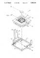
- FIG 1is an exploded perspective view of a high-density integrated circuit chip burn-in socket 10 constructed in accordance with the preferred embodiment of the present invention.
- chip burn-in socket 10comprises two principal sections, socket unit 20 and socket frame 21 into which socket unit 20 fits.
- Socket unit 20receives integrated circuit chip 11.
- Socket unit 20comprises socket block 24 from which extend connector pins 26.
- At the uppermost surface of socket block 24appears ground plate 13 to which attach wire bondings 25 which in turn, connect to connection circuit 32.
- Next 28adjoins connection circuit 32 and comprises orientation holes 101, 102 and nest opening 12.
- Integrated circuit chip 11fits within nest opening 12 and connects to connection leads 33 of connection circuit 32, as will be seen.
- Socket frame 21includes corner supports 14, frame wall 23, and frame lid 22.
- Compression spring 29mounts to frame lid 22 by pivoting lid hinge 203 and connects frame lid 22 to socket frame 21.
- latch 200attaches to frame wall 203.
- Notch 200comprises latch base 202 through which latch pin 201 moves.
- nest opening 12 of nest 28is precisely defined to receive integrated circuit chip 11.
- Orientation holes 101 and 102assure proper positioning when installing nest 28 over connection circuit 32.
- Socket frame 21receives socket unit 20 with frame walls 23 surrounding the perimeter of socket block 24.
- Connector pins 26, when socket unit 20 is within socket frame 21,extend below socket frame 21 to permit connection with test circuitry not shown.
- frame lid 22is designed to close over socket unit 20.
- Latch 200is designed to secure frame lid 22 over socket unit 20 by extending latch pin 201 over lid tip 205, thereby holding chip 11 firmly within nest 28.
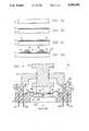
- FIG. 2is a cross-sectional schematic view of the integrated chip burn-in socket 10 of FIG. 1.
- FIG. 2shows socket unit 20 mounted within socket frame 21.
- Frame lid 22pivots on lid hinge 203 and is secured over frame walls 23 by latch 200.
- Latch 200comprises latch pin 201 which fits through latch base 202 and over lid tip 205.
- Compression spring 29mounts to frame lid 22 and presses integrated circuit chip 11 against solder bumps 33.
- Solder bumps 33attach to connection circuit 32 and provide an electrical connection to chip 11.
- Connection circuit 32adjoins compliant layer 31 and has wire bondings 25 that connect to connector pins 26.
- Connector pins 26penetrate through socket block 24 and extend sufficiently to connect to appropriate test circuitry and provide an electrical path between wire bondings 25 and the test circuitry.
- Compliant layer 31adjoins substrate 30 which attaches to foundation plate 27. Foundation plate 27 mounts within socket block 24.
- Compression spring 29in the preferred embodiment, comprises a blade spring with a blade section that exerts a positive spring force against integrated circuit chip 11 when frame lid 22 is locked in position.
- An alternative embodiment to the blade spring configuration of compression spring 29may be a screw assembly that may attach to the outer surface of frame lid 22 and extend through frame lid 22 to direct a variable positive pressure against integrated circuit chip 11. Thus, screwing the compression screw against the back surface of integrated circuit chip 11 assures positive engagement between solder bumps 33 and integrated circuit chip 11.
- a critical design parameter of the present inventionis the size and orientation of nest opening 12 (FIG. 1) that receives integrated circuit chip 11.
- Nest opening 12must be only slightly larger than the planar area of integrated circuit chip 11.
- Nest opening 12has an orientation that permits the connection points of integrated circuit chip 11 to mate precisely with solder bumps 33.
- Connection circuit 32is modeled from the data base of the integrated circuit chip to be tested.
- the data base of the integrated circuit chip 11can be adapted to form test connection circuit 32.
- This integrated circuitcan be formed by known integrated circuit fabrication techniques including etching a thin metal layer to form the integrated circuit.
- FIG. 2shows a solder bump 33 to connect to integrated circuit chip 11, this assumes that there is an associated landing pad on the chip 11. If, instead, chip 11 has a solder bump with which connection circuit 32 must associate, a landing pad on connection circuit 32 can replace solder bump 33.
- Compliant layer 31may be any compliant material that can be deposited by semiconductor device fabrication techniques and which has sufficient compliance properties for the purposes of the present invention as will be discussed.
- Substrates 30comprises a silicon material but may be another material such-as quartz, depending on desired material and conducted properties.
- Substrate 30attaches to foundation plate 27 by adhesive or other means.
- Foundation plate 27has a outwardly bevelled edge that anchors foundation plate 27. Through a bonded layer between foundation plate 27 and substrate 30, the remainder of socket test head 34 rigidly mounts within socket block 24.
- socket unit 20 componentsuse various materials.
- nest 28comprises a ceramic material in which a laser drill may cut orientation holes 101 and 102 as well as nest opening 12.
- Connection circuit 32, wire bondings 25, and connector pins 26may comprise a tungstenized gold material that provides sufficient strength and electrical conductivity for the needs of the present invention.
- Solder bumps 33may use a tungstenized gold alloy for electrical connection to connection circuit 32.
- Compliant layer 31may be a polyimide layer for which compressive properties vary as a function of layer thickness.
- Substrate 30may be silicon, although other rigid materials may be used.
- Foundation plate 27may also comprise silicon or other material sufficient to rigidly anchor socket test head 34 thereto with the use of epoxy or one other adhesive. Additionally, and adhesive may be used to affix nest 28 firmly to connection circuit 32.
- FIGS. 3 and 4are related and show compressive properties that compliant layer 31 may possess to absorb planarity differences between connections on integrated circuit chip 11 and solder bumps 33 of socket test head 34.
- FIG. 3shows a representative engagement of integrated circuit chip 11 with socket test head 34.
- integrated circuit chip 11includes landing pads 301, 302, 303 and 304 which receive solder bumps 33, including individual bumps 331, 332, 333 and 334. Solder bumps attach to respective connection circuit which attach to compliant layer 31. Compliant layer 31 mounts to substrate 30.
- solder bump 331mates with landing pad 301 without any compression of compliant layer 31.
- Solder bumps 333 and 334mate with pads 303 and 304 and make depressions of approximately equal magnitude within compliant layer 31 upon their respective engagements.
- the connection between landing pad 302 and solder bump 333makes an even larger depression in compliant layer 31.
- Compliant layer 31absorbs this difference however. Note that rigid substrate 30 evenly distributes force among the four connections of FIG. 3, and compliant layer 31 cooperates to assure positive connection among all four landing pad-solder bump combinations.
- FIG. 4illustrates the relationship between compliant layer 31 compression and load using as compliant layer 31 a material having the trade name Hitachi PIQ 3600 with a load area of 6.22 ⁇ 10 -3 cm 2 .
- FIG. 4illustrated that as the load upon compliant layer 31 increases, the compression as a percent of initial thickness also increases in approximately linearly. With this information, it is a simple matter to determine the necessary thickness of compliant layer 31. In other words, the thickness may be adjusted as a function of the anticipated planarity differences that compliant layer 31 must absorb. Obviously, if materials other that Hitachi PIQ 3600 are used for compliant layer 31, a similar compression versus load characteristic curve can be generated. Different materials may also require varying thicknesses of complaint layer 31 for anticipated planarity differences and loads.
- FIGS. 5a-dprovide cross-sectional views of a segment of socket test head 34, that illustrates the use of known semiconductor fabrication techniques.
- the fabrication technique that FIGS. 5 a-d illustrateis similar to those shown in U.S. Pat. application Ser. No. 07/560,398, filed July 31, 1990, entitled "High Performance AC Test Head,” by Kwon et. al., who are also co-inventors of the present invention, which patent application in its entirety is hereby incorporated.
- FIGS. 5a-dbegins with a silicon substrate of sufficient thickness for the present invention.
- FIG. 5bshows the application of a thin polyimide coat to serve as compliant layer 31 on substrate 30.
- Polyimide coat 31can be applied using known semiconductor fabrication techniques.
- FIG. 5cshows the creation of connection circuit 32 over compliant layer 31. Connection circuit 32 appears as a result of depositing metal on the top of polyimide film 31 and etching or otherwise patterning the layer to provide an electrical path forming connection circuit 32 for connecting the integrated circuit chip to the test circuitry.
- FIG. 5dshows the creation of solder bump 33 serving as connection lead 33.
- Metal bump 33is a hard metal material coated with tungstenized gold that can provide positive connection between integrated circuit chip 11 and connection circuit 32.
- FIG. 6is a schematic cross-sectional view of an alternative embodiment of the present invention.
- socket frame 60performs a similar function to socket frame 20, however, socket frame 60 assures good electrical contact between connection leads 33 and landing pads on integrated circuit chip 11.
- socket frame 60includes thread engaged pedestal 601 which mounts on threads within pedestal frame 602.
- Pedestal frame 602attaches to socket frame lid 609 which includes x-direction adjustor at 603, radial adjustor 604 and y-direction adjustor 605.
- Socket frame 60further includes socket frame base 620 into which mount connector pins 626 and ground pins 627. Within the center of socket frame base 610 is transparent window 608.
- Connector pins 620have attached to them bonding wires 25 which connect to connection circuit 32 of socket test head 64.
- Clear foundation plate 27attaches to transparent material window 608 and anchors socket test head 64 to socket frame base 610.
- Socket test head 64comprises within substrate 30 a transparent material 607 and transparent compliant material 606. A line of sight exists in the embodiment of FIG. 6 beginning at transparent material 608, continuing through clear foundation plate 27, base 607 and clear compliant layer 606.
- FIG. 6does not have the nest arrangement of FIGS. 1-5, this alternative arrangement provides a pedestal-type holder 601 that holds integrated circuit chip 11 and permit movement in the x,y,z, and ⁇ directions. This allows alignment of integrated circuit chip 11 up over connection circuit 32.
- the configuration of FIG. 6also provides a way to scrub contact pads of oxides and other unnecessary and obstructive materials, whether on the socket test head 34 or integrated circuit chip 11 by permitting appropriate x, y, z or ⁇ movement.
Landscapes
- Engineering & Computer Science (AREA)
- Computer Hardware Design (AREA)
- Microelectronics & Electronic Packaging (AREA)
- Physics & Mathematics (AREA)
- General Physics & Mathematics (AREA)
- General Engineering & Computer Science (AREA)
- Environmental & Geological Engineering (AREA)
- Testing Of Individual Semiconductor Devices (AREA)
Abstract
Description
This invention relates in general to integrated circuit testing, and more particularly to an integrated circuit chip burn-in socket and method.
Electronic systems often comprise many individual integrated circuit chips packaged together in a multiple integrated circuit chip module. Multiple-chip module assembly methods include a test known as integrated circuit chip burn-in testing. Burn-in testing includes operating the integrated circuits at a higher than normal operating temperature and voltage to overstress the chips. These tests assure that integrated circuits being tested can satisfy normal operating conditions for which they are designed.
Multiple-chip modules have leads that permit easy electrical connection to the individual chips. At one time, integrated circuit chips were often more expensive than the packaging to which they were attached in forming multiple chip modules. Furthermore, earlier multi-chip integrated circuit modules had fewer chips per module. As a result, it made sense to first assemble integrated circuit chips to the multiple-chip module packaging and then test the individual chips. If a chip failed, the entire module would be discarded. The combined cost and difficulty of testing and perhaps having to discard the entire multiple-chip module, however, was usually less than that of testing and perhaps having to discard the smaller individual chips.
Today's more sophisticated and complicated integrated circuits and packaging technologies have significantly changed cost considerations for integrated circuit module fabrication. With more expensive packaging for complicated integrated circuit modules, as well as reduced integrated circuit fabrication costs, in many cases a significantly larger portion of total fabrication costs go to the packages supporting integrated circuit chips. For complicated circuits and their supporting packaging, it no longer makes economic sense to discard the entire multiple-chip module in the event of a failed integrated circuit chip.
Consequently, there is a need for a device and method that permits integrated circuit chip testing prior to assembly into a multiple-chip integrated circuit module.
Some attempts have been made to overcome limitations associated with test devices that can only test integrated circuits after packaging. For example, U.S. Pat. application Ser. No. 330,839, filed Mar. 30, 1989, entitled "Flip Chip Test Socket Adapter and Method" by S. Malhi, et al., incorporated by reference herein, describes a test socket adapter. That application discloses a method and apparatus for allowing bare chips, i.e., integrated circuit chips prior to packaging, to be tested for burn-in testing. In the Malhi test socket adapter, a bare integrated circuit chip may be inserted into and held. Cantilever beams on the Malhi device deflect and compensate for planarity variations at electrical connections when the chip engages the test socket adapter. The deflection of the cantilever beams allows a positive contact between the test connections and the cantilever beams for burn-in testing.
While the Malhi disclosure solves numerous problems associated with integrated circuit chip testing, significant improvement in such devices is yet necessary. In particular, the cantilever beam structure can only accommodate an integrated circuit chip having a line array of landing pads or solder bumps. That is, only if the integrated circuit test connections surround the perimeter of integrated circuit chip can the cantilever beam structure test the integrated circuit chip. While numerous integrated circuit chips have such a configuration, more complex high performance integrated circuit chips use test connections interior to the perimeter of integrated circuit chip. Additionally, the mechanical structure and materials of the cantilever beams allows no greater separation between the beams than approximately 100 microns. These two problems limit the complexity or, similarly, the test connection density (i.e., number of test connections per unit area) that the test socket adapter can accommodate. Furthermore, the cantilever beams are brittle and can be deflected no more than approximately 50 microns without breaking. This imposes a limit on the planarity differences that can exist between the integrated circuit chip and the adapter.
Thus, there is a need for an integrated circuit chip socket adapter that can provide test connections interior to the perimeter of the integrated circuit chip.
There is also a need for a bare integrated circuit chip test socket that can provide greater test connection density than known devices.
Additionally, there is a need for a bare integrated circuit chip burn-in test socket that provides sufficient compliance for greater planarity differences than conventional adapters provide.
The present invention provides an apparatus and method for high performance and high density burn-in testing of bare integrated circuit chips. The invention comprises a connection circuit secured to a compliant base and a socket assembly that holds a bare integrated circuit chip to provide an electrical path from the chip to test circuitry via the connection circuit.
In accordance with one aspect of the invention, there is provided a high density integrated circuit burn-in socket for burn-in testing of a bare integrated circuit chip prior to integrating the chip with a number of other chips in a multiple-chip module. The high-density connection circuit comprises either a line array or area array of landing pads and solder bumps designed to engage respective solder bumps and landing pads on an integrated circuit chip to be tested.
The compliant base includes a substrate to which a compliant layer and an etched metal layer is attached. The metal layer includes a connection circuit, a portion of which essentially mirrors the circuits of the integrated circuit chip design. A ceramic disk, called a nest, adjoins the metal layer and receives the bare integrated circuit chip to assure proper alignment between integrated circuit chip and the connection circuit of the metal layer. A socket assembly receives the compliant base and includes-connections from the metal layer connection circuit through to test circuitry. Additionally, the socket assembly provides a securing mechanism to assure positive engagement of the bare integrated circuit chip within the nest.
In a further aspect of the invention, the compliant insulator comprises a layer of polyimide or other compliant material having a sufficient thickness and compliance to absorb anticipated planarity differences between integrated circuit test connections and the connection circuit. The connection circuit is designed to have solder bumps to engage integrated circuit landing pads. Alternatively, where the integrated circuit chip connection has its own solder bumps, the connection circuit design associates a landing pad with each such solder bump to electrically mate with the integrated circuit chip solder bump.
A technical advantage of the present invention is that it permits bare integrated circuit chip testing prior to the integrated circuit chip being integrated with a number of chips in a multiple-chip module. This can significantly reduce multiple-chip module fabrication costs.
Another technical advantage of the present invention is that the connection circuit is made from an etched metal layer. The present invention can provide a larger number of electrical connections per unit area between the bare integrated circuit chip and the test circuitry. This greater density is critical to the higher density test connections characteristic of today's more complex integrated circuit chips.
Another technical advantage is that by adhering the connection circuitry to a compliant layer, the present invention provides a more durable and resilient test circuit connection.
Yet another technical advantage of the present invention is that by applying the metal layer to the polyimide coat and etching the metal layer, it is possible to create a two-dimensional circuit having test connections extending beyond the perimeter of the integrated circuit chip. This aids in testing more complex integrated circuit chips.
Moreover, the combination of high density integrated circuit chip test connection circuitry and the ability of the present invention to make connections within the perimeter of the integrated circuit chip is a further technical advantage of the present invention.
For a more complete understanding of the present invention and for further advantages thereof, reference is now made to the following detailed description, taken in conjunction with the accompanying FIGURES, in which:
FIG. 1 is a perspective view of a high density integrated circuit chip test socket constructed in accordance with a preferred embodiment of the present invention;
FIG. 2 is a cross-sectional schematic view of the chip burn-in socket of FIG. 1;
FIG. 3 is a cross-sectional schematic view of an integrated circuit chip engaging the connection circuit according to a preferred embodiment of the present invention;
FIG. 4 is an empirically determined plot of compression versus load for a polyimide film used in a preferred embodiment of the present invention;
FIGS. 5a-d are cross-sectional views of a method for constructing the compliant base and connection circuit of the socket test head of a preferred embodiment of the present invention; and
FIG. 6 is a schematic cross-sectional view of an alternative embodiment of the present invention.
The preferred embodiment of the present invention is best understood by referring to the FIGURES, like numerals being used for like and corresponding parts of the various drawings.
FIG 1 is an exploded perspective view of a high-density integrated circuit chip burn-insocket 10 constructed in accordance with the preferred embodiment of the present invention. According to FIG. 1, chip burn-insocket 10 comprises two principal sections,socket unit 20 andsocket frame 21 into whichsocket unit 20 fits.Socket unit 20 receives integratedcircuit chip 11.Socket unit 20 comprisessocket block 24 from which extend connector pins 26. At the uppermost surface ofsocket block 24 appearsground plate 13 to which attachwire bondings 25 which in turn, connect toconnection circuit 32. Next 28 adjoinsconnection circuit 32 and comprises orientation holes 101, 102 andnest opening 12. Integratedcircuit chip 11 fits withinnest opening 12 and connects to connection leads 33 ofconnection circuit 32, as will be seen.
As FIG. 1 indicates, nest opening 12 ofnest 28 is precisely defined to receiveintegrated circuit chip 11. Orientation holes 101 and 102 assure proper positioning when installingnest 28 overconnection circuit 32.Socket frame 21 receivessocket unit 20 withframe walls 23 surrounding the perimeter ofsocket block 24. Connector pins 26, whensocket unit 20 is withinsocket frame 21, extend belowsocket frame 21 to permit connection with test circuitry not shown. Withsocket unit 20 insocket frame 21,frame lid 22 is designed to close oversocket unit 20.Latch 200 is designed to secureframe lid 22 oversocket unit 20 by extendinglatch pin 201 overlid tip 205, thereby holdingchip 11 firmly withinnest 28.
FIG. 2 is a cross-sectional schematic view of the integrated chip burn-insocket 10 of FIG. 1. FIG. 2 showssocket unit 20 mounted withinsocket frame 21.Frame lid 22 pivots onlid hinge 203 and is secured overframe walls 23 bylatch 200.Latch 200 compriseslatch pin 201 which fits throughlatch base 202 and overlid tip 205.Compression spring 29 mounts to framelid 22 and presses integratedcircuit chip 11 against solder bumps 33. Solder bumps 33 attach toconnection circuit 32 and provide an electrical connection tochip 11.Connection circuit 32 adjoinscompliant layer 31 and has wire bondings 25 that connect to connector pins 26. Connector pins 26 penetrate throughsocket block 24 and extend sufficiently to connect to appropriate test circuitry and provide an electrical path betweenwire bondings 25 and the test circuitry.Compliant layer 31 adjoinssubstrate 30 which attaches tofoundation plate 27.Foundation plate 27 mounts withinsocket block 24.
A critical design parameter of the present invention is the size and orientation of nest opening 12 (FIG. 1) that receives integratedcircuit chip 11. Nest opening 12 must be only slightly larger than the planar area ofintegrated circuit chip 11. Nest opening 12 has an orientation that permits the connection points ofintegrated circuit chip 11 to mate precisely with solder bumps 33.
In the preferred embodiment of the present invention,socket unit 20 components use various materials. For example,nest 28 comprises a ceramic material in which a laser drill may cutorientation holes nest opening 12.Connection circuit 32,wire bondings 25, and connector pins 26 may comprise a tungstenized gold material that provides sufficient strength and electrical conductivity for the needs of the present invention. Solder bumps 33 may use a tungstenized gold alloy for electrical connection toconnection circuit 32.Compliant layer 31 may be a polyimide layer for which compressive properties vary as a function of layer thickness.Substrate 30 may be silicon, although other rigid materials may be used.Foundation plate 27 may also comprise silicon or other material sufficient to rigidly anchorsocket test head 34 thereto with the use of epoxy or one other adhesive. Additionally, and adhesive may be used to affixnest 28 firmly toconnection circuit 32.
FIGS. 3 and 4 are related and show compressive properties thatcompliant layer 31 may possess to absorb planarity differences between connections onintegrated circuit chip 11 and solder bumps 33 ofsocket test head 34.
FIG. 3 shows a representative engagement ofintegrated circuit chip 11 withsocket test head 34. In FIG. 3, integratedcircuit chip 11 includeslanding pads solder bumps 33, includingindividual bumps compliant layer 31.Compliant layer 31 mounts tosubstrate 30.
As FIG. 3 shows,solder bump 331 mates withlanding pad 301 without any compression ofcompliant layer 31. Solder bumps 333 and 334, however, mate withpads compliant layer 31 upon their respective engagements. The connection betweenlanding pad 302 andsolder bump 333 makes an even larger depression incompliant layer 31.Compliant layer 31 absorbs this difference however. Note thatrigid substrate 30 evenly distributes force among the four connections of FIG. 3, andcompliant layer 31 cooperates to assure positive connection among all four landing pad-solder bump combinations.
FIG. 4 illustrates the relationship betweencompliant layer 31 compression and load using as compliant layer 31 a material having the trade name Hitachi PIQ 3600 with a load area of 6.22×10⁻³ cm2. FIG. 4 illustrated that as the load uponcompliant layer 31 increases, the compression as a percent of initial thickness also increases in approximately linearly. With this information, it is a simple matter to determine the necessary thickness ofcompliant layer 31. In other words, the thickness may be adjusted as a function of the anticipated planarity differences thatcompliant layer 31 must absorb. Obviously, if materials other that Hitachi PIQ 3600 are used forcompliant layer 31, a similar compression versus load characteristic curve can be generated. Different materials may also require varying thicknesses ofcomplaint layer 31 for anticipated planarity differences and loads.
FIGS. 5a-d provide cross-sectional views of a segment ofsocket test head 34, that illustrates the use of known semiconductor fabrication techniques. The fabrication technique that FIGS. 5 a-d illustrate is similar to those shown in U.S. Pat. application Ser. No. 07/560,398, filed July 31, 1990, entitled "High Performance AC Test Head," by Kwon et. al., who are also co-inventors of the present invention, which patent application in its entirety is hereby incorporated.
The fabrication sequence of FIGS. 5a-d begins with a silicon substrate of sufficient thickness for the present invention. FIG. 5b shows the application of a thin polyimide coat to serve ascompliant layer 31 onsubstrate 30.Polyimide coat 31 can be applied using known semiconductor fabrication techniques. FIG. 5c shows the creation ofconnection circuit 32 overcompliant layer 31.Connection circuit 32 appears as a result of depositing metal on the top ofpolyimide film 31 and etching or otherwise patterning the layer to provide an electrical path formingconnection circuit 32 for connecting the integrated circuit chip to the test circuitry. FIG. 5d shows the creation ofsolder bump 33 serving asconnection lead 33.Metal bump 33 is a hard metal material coated with tungstenized gold that can provide positive connection betweenintegrated circuit chip 11 andconnection circuit 32.
FIG. 6 is a schematic cross-sectional view of an alternative embodiment of the present invention. In this embodiment,socket frame 60 performs a similar function tosocket frame 20, however,socket frame 60 assures good electrical contact between connection leads 33 and landing pads onintegrated circuit chip 11. In FIG. 6,socket frame 60 includes thread engagedpedestal 601 which mounts on threads withinpedestal frame 602.Pedestal frame 602 attaches tosocket frame lid 609 which includes x-direction adjustor at 603,radial adjustor 604 and y-direction adjustor 605.Socket frame 60 further includes socket frame base 620 into which mount connector pins 626 and ground pins 627. Within the center ofsocket frame base 610 istransparent window 608.
Connector pins 620 have attached to them bondingwires 25 which connect toconnection circuit 32 ofsocket test head 64.Clear foundation plate 27 attaches totransparent material window 608 and anchorssocket test head 64 tosocket frame base 610.Socket test head 64, comprises within substrate 30 atransparent material 607 and transparentcompliant material 606. A line of sight exists in the embodiment of FIG. 6 beginning attransparent material 608, continuing throughclear foundation plate 27,base 607 and clearcompliant layer 606.
Although the configuration of FIG. 6 does not have the nest arrangement of FIGS. 1-5, this alternative arrangement provides a pedestal-type holder 601 that holds integratedcircuit chip 11 and permit movement in the x,y,z, and Θ directions. This allows alignment ofintegrated circuit chip 11 up overconnection circuit 32. The configuration of FIG. 6 also provides a way to scrub contact pads of oxides and other unnecessary and obstructive materials, whether on thesocket test head 34 or integratedcircuit chip 11 by permitting appropriate x, y, z or Θ movement. There may be other possible configurations within the scope of the present invention to allow ease of alignment, insertion, and removal of theintegrated circuit chip 11 for AC and burn-in testing.
Although the invention has been described with reference to the above specific embodiments, this description is not meant to be construed in a limiting sense. Various modifications of a disclosed embodiment, as well as alternative embodiments of the invention will become apparent to persons skilled in the art upon reference to the above description. It is further contemplated that the appended claims will cover such modifications that fall within the true scope of the invention.
Claims (7)
1. A method for forming an apparatus for urn-in testing of a base integrated circuit chip comprising the steps of:
forming a substrate;
forming a compliant layer over said substrate;
forming a connection circuit over said compliant layer; and
forming an est to receive the integrated circuit chip over said connection circuit.
2. The method of claim 1, further comprising the step of forming solder bumps and landing pads on said connection circuit to connect between said connection circuit and the integrated circuit chip.
3. A method for forming an apparatus for burn-in testing of a base integrated circuit chip comprising the steps of:
forming a substrate;
forming a compliant layer over said substrate such that said substrate and said compliant layer forms a base;
forming a connection circuit over said compliant layer; and
4. The method of claim 3, further comprising the steps of forming solder bumps and landing pads on said connection circuit to connect between said connection circuit and the integrated circuit chip.
5. The method of claim 3, further comprising the step of forming a nest to receive the integrated circuit chip over said connection circuit.
6. The method of claim 3, further comprising the steps of providing a plurality of connecting pins suitable for connecting said block to test circuitry and connecting a plurality of wire bonds between said connection circuitry to said plurality of pins.
7. The method of claim 5 and further comprising the steps of providing a plurality of connecting pins suitable for connecting said block to test circuitry and connecting a plurality of wire bonds between said connection circuitry to said plurality of pins.
Priority Applications (1)
| Application Number | Priority Date | Filing Date | Title |
|---|---|---|---|
| US07/575,456US5088190A (en) | 1990-08-30 | 1990-08-30 | Method of forming an apparatus for burn in testing of integrated circuit chip |
Applications Claiming Priority (1)
| Application Number | Priority Date | Filing Date | Title |
|---|---|---|---|
| US07/575,456US5088190A (en) | 1990-08-30 | 1990-08-30 | Method of forming an apparatus for burn in testing of integrated circuit chip |
Publications (1)
| Publication Number | Publication Date |
|---|---|
| US5088190Atrue US5088190A (en) | 1992-02-18 |
Family
ID=24300397
Family Applications (1)
| Application Number | Title | Priority Date | Filing Date |
|---|---|---|---|
| US07/575,456Expired - LifetimeUS5088190A (en) | 1990-08-30 | 1990-08-30 | Method of forming an apparatus for burn in testing of integrated circuit chip |
Country Status (1)
| Country | Link |
|---|---|
| US (1) | US5088190A (en) |
Cited By (99)
| Publication number | Priority date | Publication date | Assignee | Title |
|---|---|---|---|---|
| US5289631A (en)* | 1992-03-04 | 1994-03-01 | Mcnc | Method for testing, burn-in, and/or programming of integrated circuit chips |
| FR2705522A1 (en)* | 1993-05-14 | 1994-11-25 | Samsung Electronics Co Ltd | Apparatus and method for debugging test |
| US5376010A (en)* | 1994-02-08 | 1994-12-27 | Minnesota Mining And Manufacturing Company | Burn-in socket |
| US5389819A (en)* | 1992-12-10 | 1995-02-14 | Yamaichi Electronics Co., Ltd. | Socket for an IC carrier having a flexible wiring sheet superimposed over an IC body and an elastic backup member elastically pressing the flexible wiring sheet into contact with the IC body |
| EP0614089A3 (en)* | 1993-03-01 | 1995-07-12 | Ibm | Method and apparatus for in-situ testing of integrated circuit chips. |
| US5451165A (en)* | 1994-07-27 | 1995-09-19 | Minnesota Mining And Manufacturing Company | Temporary package for bare die test and burn-in |
| US5483741A (en)* | 1993-09-03 | 1996-01-16 | Micron Technology, Inc. | Method for fabricating a self limiting silicon based interconnect for testing bare semiconductor dice |
| US5487999A (en)* | 1991-06-04 | 1996-01-30 | Micron Technology, Inc. | Method for fabricating a penetration limited contact having a rough textured surface |
| US5495179A (en)* | 1991-06-04 | 1996-02-27 | Micron Technology, Inc. | Carrier having interchangeable substrate used for testing of semiconductor dies |
| US5519332A (en)* | 1991-06-04 | 1996-05-21 | Micron Technology, Inc. | Carrier for testing an unpackaged semiconductor die |
| US5523586A (en)* | 1993-09-20 | 1996-06-04 | Kabushiki Kaisha Toshiba | Burn-in socket used in a burn-in test for semiconductor chips |
| US5541525A (en)* | 1991-06-04 | 1996-07-30 | Micron Technology, Inc. | Carrier for testing an unpackaged semiconductor die |
| US5543725A (en)* | 1993-08-25 | 1996-08-06 | Sunright Limited | Reusable carrier for burn-in/testing on non packaged die |
| US5559444A (en)* | 1991-06-04 | 1996-09-24 | Micron Technology, Inc. | Method and apparatus for testing unpackaged semiconductor dice |
| US5578934A (en)* | 1991-06-04 | 1996-11-26 | Micron Technology, Inc. | Method and apparatus for testing unpackaged semiconductor dice |
| US5581875A (en)* | 1994-02-18 | 1996-12-10 | Murata Manufacturing Co., Ltd. | Method of manufacturing circuit module |
| US5585282A (en)* | 1991-06-04 | 1996-12-17 | Micron Technology, Inc. | Process for forming a raised portion on a projecting contact for electrical testing of a semiconductor |
| US5589781A (en)* | 1990-09-20 | 1996-12-31 | Higgins; H. Dan | Die carrier apparatus |
| EP0768534A1 (en)* | 1995-10-09 | 1997-04-16 | Nitto Denko Corporation | Method for fabrication of probe structure and circuit substrate therefor |
| US5633122A (en)* | 1993-08-16 | 1997-05-27 | Micron Technology, Inc. | Test fixture and method for producing a test fixture for testing unpackaged semiconductor die |
| US5634267A (en)* | 1991-06-04 | 1997-06-03 | Micron Technology, Inc. | Method and apparatus for manufacturing known good semiconductor die |
| US5691649A (en)* | 1991-06-04 | 1997-11-25 | Micron Technology, Inc. | Carrier having slide connectors for testing unpackaged semiconductor dice |
| US5705933A (en)* | 1993-08-25 | 1998-01-06 | Sunright Limited | Resuable carrier for burn-in/testing on non packaged die |
| US5716218A (en)* | 1991-06-04 | 1998-02-10 | Micron Technology, Inc. | Process for manufacturing an interconnect for testing a semiconductor die |
| US5721496A (en)* | 1996-01-23 | 1998-02-24 | Micron Technology, Inc. | Method and apparatus for leak checking unpackaged semiconductor dice |
| US5739050A (en)* | 1996-01-26 | 1998-04-14 | Micron Technology, Inc. | Method and apparatus for assembling a semiconductor package for testing |
| US5742169A (en)* | 1996-02-20 | 1998-04-21 | Micron Technology, Inc. | Apparatus for testing interconnects for semiconductor dice |
| US5756370A (en)* | 1996-02-08 | 1998-05-26 | Micron Technology, Inc. | Compliant contact system with alignment structure for testing unpackaged semiconductor dice |
| US5783461A (en)* | 1996-10-03 | 1998-07-21 | Micron Technology, Inc. | Temporary semiconductor package having hard-metal, dense-array ball contacts and method of fabrication |
| US5808360A (en)* | 1996-05-15 | 1998-09-15 | Micron Technology, Inc. | Microbump interconnect for bore semiconductor dice |
| US5815000A (en)* | 1991-06-04 | 1998-09-29 | Micron Technology, Inc. | Method for testing semiconductor dice with conventionally sized temporary packages |
| US5825195A (en)* | 1992-06-10 | 1998-10-20 | Micron Technology, Inc. | Method and apparatus for testing an unpackaged semiconductor die |
| US5834945A (en)* | 1996-12-31 | 1998-11-10 | Micron Technology, Inc. | High speed temporary package and interconnect for testing semiconductor dice and method of fabrication |
| US5872449A (en)* | 1996-01-26 | 1999-02-16 | Lsi Logic Corporation | Semiconductor package qualification chip |
| US5894218A (en)* | 1994-04-18 | 1999-04-13 | Micron Technology, Inc. | Method and apparatus for automatically positioning electronic dice within component packages |
| USRE36217E (en)* | 1995-02-06 | 1999-06-01 | Minnesota Mining And Manufacturing Company | Top load socket for ball grid array devices |
| WO1999030174A1 (en)* | 1997-12-11 | 1999-06-17 | Micron Technology, Inc. | Test system with mechanical alignment for semiconductor chip scale packages and dice |
| US5915977A (en)* | 1997-06-02 | 1999-06-29 | Micron Technology, Inc. | System and interconnect for making temporary electrical connections with bumped semiconductor components |
| US5923179A (en)* | 1996-03-29 | 1999-07-13 | Intel Corporation | Thermal enhancing test/burn in socket for C4 and tab packaging |
| US5929647A (en)* | 1996-07-02 | 1999-07-27 | Micron Technology, Inc. | Method and apparatus for testing semiconductor dice |
| US5962921A (en)* | 1997-03-31 | 1999-10-05 | Micron Technology, Inc. | Interconnect having recessed contact members with penetrating blades for testing semiconductor dice and packages with contact bumps |
| US5982185A (en)* | 1996-07-01 | 1999-11-09 | Micron Technology, Inc. | Direct connect carrier for testing semiconductor dice and method of fabrication |
| US6007348A (en)* | 1996-05-07 | 1999-12-28 | Advanced Intercommunications Corporation | Solder ball terminal |
| US6016060A (en)* | 1997-03-25 | 2000-01-18 | Micron Technology, Inc. | Method, apparatus and system for testing bumped semiconductor components |
| US6025728A (en)* | 1997-04-25 | 2000-02-15 | Micron Technology, Inc. | Semiconductor package with wire bond protective member |
| US6040702A (en)* | 1997-07-03 | 2000-03-21 | Micron Technology, Inc. | Carrier and system for testing bumped semiconductor components |
| US6060894A (en)* | 1997-03-03 | 2000-05-09 | Micron Technology, Inc. | Temporary package, method and system for testing semiconductor dice having backside electrodes |
| US6072326A (en)* | 1997-08-22 | 2000-06-06 | Micron Technology, Inc. | System for testing semiconductor components |
| US6087845A (en)* | 1990-08-29 | 2000-07-11 | Micron Technology, Inc. | Universal wafer carrier for wafer level die burn-in |
| US6091250A (en)* | 1991-06-04 | 2000-07-18 | Micron Technology, Inc. | Discrete die burn-in for nonpackaged die |
| US6094057A (en)* | 1995-10-20 | 2000-07-25 | Kabushiki Kaisha Toshiba | Board for evaluating the characteristics of a semiconductor chip and a method for mounting a semiconductor chip thereon |
| US6094058A (en)* | 1991-06-04 | 2000-07-25 | Micron Technology, Inc. | Temporary semiconductor package having dense array external contacts |
| US6214716B1 (en) | 1998-09-30 | 2001-04-10 | Micron Technology, Inc. | Semiconductor substrate-based BGA interconnection and methods of farication same |
| US6219908B1 (en) | 1991-06-04 | 2001-04-24 | Micron Technology, Inc. | Method and apparatus for manufacturing known good semiconductor die |
| US20010002624A1 (en)* | 1993-11-16 | 2001-06-07 | Igor Y. Khandros | Tip structures. |
| US6256202B1 (en) | 2000-02-18 | 2001-07-03 | Advanced Interconnections Corporation | Integrated circuit intercoupling component with heat sink |
| US6255833B1 (en) | 1997-03-04 | 2001-07-03 | Micron Technology, Inc. | Method for testing semiconductor dice and chip scale packages |
| US6262581B1 (en)* | 1998-04-20 | 2001-07-17 | Samsung Electronics Co., Ltd. | Test carrier for unpackaged semiconducter chip |
| US6285202B1 (en) | 1999-02-19 | 2001-09-04 | Micron Technology, Inc. | Test carrier with force applying mechanism guide and terminal contact protector |
| US6285203B1 (en) | 1999-06-14 | 2001-09-04 | Micron Technology, Inc. | Test system having alignment member for aligning semiconductor components |
| US6285201B1 (en)* | 1997-10-06 | 2001-09-04 | Micron Technology, Inc. | Method and apparatus for capacitively testing a semiconductor die |
| US20010020747A1 (en)* | 1998-12-31 | 2001-09-13 | Formfactor, Inc. | Special contact points for accessing internal circuitry of an integrated circuit |
| US6294839B1 (en) | 1999-08-30 | 2001-09-25 | Micron Technology, Inc. | Apparatus and methods of packaging and testing die |
| US20010024118A1 (en)* | 1991-06-04 | 2001-09-27 | Warren M. Farnworth | Bondpad attachments having self-limiting properties for penetration of semiconductor die |
| US6297660B2 (en) | 1999-01-13 | 2001-10-02 | Micron Technology, Inc. | Test carrier with variable force applying mechanism for testing semiconductor components |
| US6332946B1 (en)* | 1998-03-12 | 2001-12-25 | International Business Machines Corporation | Method for assembling a multi-layered ceramic package |
| US6340894B1 (en) | 1991-06-04 | 2002-01-22 | Micron Technology, Inc. | Semiconductor testing apparatus including substrate with contact members and conductive polymer interconnect |
| US6353326B2 (en) | 1998-08-28 | 2002-03-05 | Micron Technology, Inc. | Test carrier with molded interconnect for testing semiconductor components |
| US6396291B1 (en) | 1999-04-23 | 2002-05-28 | Micron Technology, Inc. | Method for testing semiconductor components |
| US6429671B1 (en)* | 1998-11-25 | 2002-08-06 | Advanced Micro Devices, Inc. | Electrical test probe card having a removable probe head assembly with alignment features and a method for aligning the probe head assembly to the probe card |
| US20020132501A1 (en)* | 2001-03-16 | 2002-09-19 | Eldridge Benjamin N. | Wafer level interposer |
| US20020155728A1 (en)* | 1990-09-24 | 2002-10-24 | Tessera, Inc. | Semiconductor chip assemblies, methods of making same and components for same |
| US20020197895A1 (en)* | 1999-08-17 | 2002-12-26 | Formfactor, Inc. | Electrical contractor, especially wafer level contactor, using fluid pressure |
| US6512386B2 (en)* | 1998-12-22 | 2003-01-28 | Fujitsu Limited | Device testing contactor, method of producing the same, and device testing carrier |
| US6522125B2 (en)* | 1998-05-11 | 2003-02-18 | Advantest Corporation | Tray transfer arm, electronic component testing apparatus and tray transfer method |
| US20030097877A1 (en)* | 2001-11-27 | 2003-05-29 | Hawkes Malcolm V. | Shadow-creating apparatus |
| US20030101584A1 (en)* | 1998-06-09 | 2003-06-05 | Shigeru Matsumura | Bump and method of forming bump |
| US6593762B1 (en)* | 1999-11-01 | 2003-07-15 | Agilent Technologies, Inc. | Apparatus for testing electronic components |
| US20030174486A1 (en)* | 2002-03-15 | 2003-09-18 | Borcherding Gary W. | Limited movement system for motor switch mounted thermo-protector |
| US20030174473A1 (en)* | 2002-03-15 | 2003-09-18 | Lewis William R. | Limited movement system for motor switch mounted thermo-protector |
| US6630372B2 (en) | 1997-02-14 | 2003-10-07 | Micron Technology, Inc. | Method for routing die interconnections using intermediate connection elements secured to the die face |
| US6639416B1 (en) | 1996-07-02 | 2003-10-28 | Micron Technology, Inc. | Method and apparatus for testing semiconductor dice |
| WO2003046510A3 (en)* | 2001-11-27 | 2003-11-27 | Electro Scient Ind Inc | A shadow-creating apparatus |
| US6700782B1 (en)* | 2002-11-27 | 2004-03-02 | Intel Corporation | Apparatus and method to retain an electronic component in a precise position during assembly manufacturing |
| US6763578B2 (en) | 1988-09-30 | 2004-07-20 | Micron Technology, Inc. | Method and apparatus for manufacturing known good semiconductor die |
| US20040178813A1 (en)* | 2003-03-13 | 2004-09-16 | Hiroshi Okubo | Apparatus and method for testing electronic component |
| US20040261979A1 (en)* | 2003-06-30 | 2004-12-30 | Meng-Jen Wang | [heat sink structure] |
| US20050079763A1 (en)* | 1996-10-10 | 2005-04-14 | Lemke Timothy A. | High density connector and method of manufacture |
| US20050122690A1 (en)* | 2003-12-04 | 2005-06-09 | Dell Products L.P. | Method and apparatus for attaching a processor and corresponding heat sink to a circuit board |
| US20060017451A1 (en)* | 2000-03-23 | 2006-01-26 | Salman Akram | Substrates including alignment fences |
| US6998860B1 (en) | 1991-06-04 | 2006-02-14 | Micron Technology, Inc. | Method for burn-in testing semiconductor dice |
| US20060033517A1 (en)* | 1994-11-15 | 2006-02-16 | Formfactor, Inc. | Probe for semiconductor devices |
| US7084656B1 (en)* | 1993-11-16 | 2006-08-01 | Formfactor, Inc. | Probe for semiconductor devices |
| US20070285115A1 (en)* | 1990-08-29 | 2007-12-13 | Micron Technology, Inc. | Universal wafer carrier for wafer level die burn-in |
| US20080036100A1 (en)* | 2006-05-17 | 2008-02-14 | Tessera, Inc. | Solder elements with columnar structures and methods of making the same |
| US20100014243A1 (en)* | 2008-07-21 | 2010-01-21 | Hon Hai Precision Industry Co., Ltd. | Heat dissipation apparatus |
| WO2016192926A1 (en)* | 2015-05-29 | 2016-12-08 | Muehlbauer GmbH & Co. KG | Thermal compression apparatus comprising a spring element with variably adjustable prestressing, and method for connecting electrical components to a substrate using the thermal compression apparatus |
| US20170131347A1 (en)* | 2015-11-05 | 2017-05-11 | Shenzhen Sireda Technology Co., Ltd | Test fixture and test device for ic |
| CN112881896A (en)* | 2021-02-07 | 2021-06-01 | 荀露 | Conductive assembly and testing device |
Citations (7)
| Publication number | Priority date | Publication date | Assignee | Title |
|---|---|---|---|---|
| US3596228A (en)* | 1969-05-29 | 1971-07-27 | Ibm | Fluid actuated contactor |
| US3832769A (en)* | 1971-05-26 | 1974-09-03 | Minnesota Mining & Mfg | Circuitry and method |
| US4048438A (en)* | 1974-10-23 | 1977-09-13 | Amp Incorporated | Conductor patterned substrate providing stress release during direct attachment of integrated circuit chips |
| US4237607A (en)* | 1977-06-01 | 1980-12-09 | Citizen Watch Co., Ltd. | Method of assembling semiconductor integrated circuit |
| US4649339A (en)* | 1984-04-25 | 1987-03-10 | Honeywell Inc. | Integrated circuit interface |
| US4779340A (en)* | 1984-03-26 | 1988-10-25 | Axonix Corporation | Programmable electronic interconnect system and method of making |
| US4968589A (en)* | 1988-10-26 | 1990-11-06 | General Signal Corporation | Probe card for integrated circuit chip and method of making probe card |
- 1990
- 1990-08-30USUS07/575,456patent/US5088190A/ennot_activeExpired - Lifetime
Patent Citations (7)
| Publication number | Priority date | Publication date | Assignee | Title |
|---|---|---|---|---|
| US3596228A (en)* | 1969-05-29 | 1971-07-27 | Ibm | Fluid actuated contactor |
| US3832769A (en)* | 1971-05-26 | 1974-09-03 | Minnesota Mining & Mfg | Circuitry and method |
| US4048438A (en)* | 1974-10-23 | 1977-09-13 | Amp Incorporated | Conductor patterned substrate providing stress release during direct attachment of integrated circuit chips |
| US4237607A (en)* | 1977-06-01 | 1980-12-09 | Citizen Watch Co., Ltd. | Method of assembling semiconductor integrated circuit |
| US4779340A (en)* | 1984-03-26 | 1988-10-25 | Axonix Corporation | Programmable electronic interconnect system and method of making |
| US4649339A (en)* | 1984-04-25 | 1987-03-10 | Honeywell Inc. | Integrated circuit interface |
| US4968589A (en)* | 1988-10-26 | 1990-11-06 | General Signal Corporation | Probe card for integrated circuit chip and method of making probe card |
Cited By (216)
| Publication number | Priority date | Publication date | Assignee | Title |
|---|---|---|---|---|
| US6763578B2 (en) | 1988-09-30 | 2004-07-20 | Micron Technology, Inc. | Method and apparatus for manufacturing known good semiconductor die |
| US20070103180A1 (en)* | 1990-08-29 | 2007-05-10 | Wood Alan G | Universal wafer carrier for wafer level die burn-in |
| US7362113B2 (en) | 1990-08-29 | 2008-04-22 | Micron Technology, Inc. | Universal wafer carrier for wafer level die burn-in |
| US20030206030A1 (en)* | 1990-08-29 | 2003-11-06 | Wood Alan G. | Universal wafer carrier for wafer level die burn-in |
| US20040212391A1 (en)* | 1990-08-29 | 2004-10-28 | Wood Alan G. | Method for universal wafer carrier for wafer level die burn-in |
| US6535012B1 (en) | 1990-08-29 | 2003-03-18 | Micron Technology, Inc. | Universal wafer carrier for wafer level die burn-in |
| US6087845A (en)* | 1990-08-29 | 2000-07-11 | Micron Technology, Inc. | Universal wafer carrier for wafer level die burn-in |
| US6091254A (en)* | 1990-08-29 | 2000-07-18 | Micron Technology, Inc. | Universal wafer carrier for wafer level die burn-in |
| US20050237075A1 (en)* | 1990-08-29 | 2005-10-27 | Wood Alan G | Method for testing using a universal wafer carrier for wafer level die burn-in |
| US20050237077A1 (en)* | 1990-08-29 | 2005-10-27 | Wood Alan G | Method for testing using a universal wafer carrier for wafer level die burn-in |
| US20050237076A1 (en)* | 1990-08-29 | 2005-10-27 | Wood Alan G | Method for testing using a universal wafer carrier for wafer level die burn-in |
| US20050253619A1 (en)* | 1990-08-29 | 2005-11-17 | Wood Alan G | Method for testing using a universal wafer carrier for wafer level die burn-in |
| US7112985B2 (en) | 1990-08-29 | 2006-09-26 | Micron Technology, Inc. | Method for testing using a universal wafer carrier for wafer level die burn-in |
| US6737882B2 (en) | 1990-08-29 | 2004-05-18 | Micron Technology, Inc. | Method for universal wafer carrier for wafer level die burn-in |
| US7112986B2 (en) | 1990-08-29 | 2006-09-26 | Micron Technology, Inc. | Method for testing using a universal wafer carrier for wafer level die burn-in |
| US20050253620A1 (en)* | 1990-08-29 | 2005-11-17 | Wood Alan G | Method for testing using a universal wafer carrier for wafer level die burn-in |
| US7141997B2 (en) | 1990-08-29 | 2006-11-28 | Micron Technology, Inc. | Method for testing using a universal wafer carrier for wafer level die burn-in |
| US7161373B2 (en) | 1990-08-29 | 2007-01-09 | Micron Technology, Inc. | Method for testing using a universal wafer carrier for wafer level die burn-in |
| US7167012B2 (en) | 1990-08-29 | 2007-01-23 | Micron Technology, Inc. | Universal wafer carrier for wafer level die burn-in |
| US6342789B1 (en) | 1990-08-29 | 2002-01-29 | Micron Technology, Inc. | Universal wafer carrier for wafer level die burn-in |
| US7167014B2 (en) | 1990-08-29 | 2007-01-23 | Micron Technology, Inc. | Method for testing using a universal wafer carrier for wafer level die burn-in |
| US7511520B2 (en) | 1990-08-29 | 2009-03-31 | Micron Technology, Inc. | Universal wafer carrier for wafer level die burn-in |
| US7288953B2 (en) | 1990-08-29 | 2007-10-30 | Micron Technology, Inc. | Method for testing using a universal wafer carrier for wafer level die burn-in |
| US20070285115A1 (en)* | 1990-08-29 | 2007-12-13 | Micron Technology, Inc. | Universal wafer carrier for wafer level die burn-in |
| US5589781A (en)* | 1990-09-20 | 1996-12-31 | Higgins; H. Dan | Die carrier apparatus |
| US7291910B2 (en) | 1990-09-24 | 2007-11-06 | Tessera, Inc. | Semiconductor chip assemblies, methods of making same and components for same |
| US20020155728A1 (en)* | 1990-09-24 | 2002-10-24 | Tessera, Inc. | Semiconductor chip assemblies, methods of making same and components for same |
| US20050087855A1 (en)* | 1990-09-24 | 2005-04-28 | Tessera, Inc. | Microelectronic component and assembly having leads with offset portions |
| US5815000A (en)* | 1991-06-04 | 1998-09-29 | Micron Technology, Inc. | Method for testing semiconductor dice with conventionally sized temporary packages |
| US6219908B1 (en) | 1991-06-04 | 2001-04-24 | Micron Technology, Inc. | Method and apparatus for manufacturing known good semiconductor die |
| US6091251A (en)* | 1991-06-04 | 2000-07-18 | Wood; Alan G. | Discrete die burn-in for nonpackaged die |
| US5796264A (en)* | 1991-06-04 | 1998-08-18 | Micron Technology, Inc. | Apparatus for manufacturing known good semiconductor dice |
| US5691649A (en)* | 1991-06-04 | 1997-11-25 | Micron Technology, Inc. | Carrier having slide connectors for testing unpackaged semiconductor dice |
| US6222379B1 (en) | 1991-06-04 | 2001-04-24 | Micron Technology, Inc. | Conventionally sized temporary package for testing semiconductor dice |
| US6265245B1 (en) | 1991-06-04 | 2001-07-24 | Micron Technology, Inc. | Compliant interconnect for testing a semiconductor die |
| US20040214409A1 (en)* | 1991-06-04 | 2004-10-28 | Warren Farnworth | Method and apparatus for manufacturing known good semiconductor die |
| US6091250A (en)* | 1991-06-04 | 2000-07-18 | Micron Technology, Inc. | Discrete die burn-in for nonpackaged die |
| US5844418A (en)* | 1991-06-04 | 1998-12-01 | Micron Technology, Inc. | Carrier having interchangeable substrate used for testing of semiconductor dies |
| US6828812B2 (en)* | 1991-06-04 | 2004-12-07 | Micron Technology, Inc. | Test apparatus for testing semiconductor dice including substrate with penetration limiting contacts for making electrical connections |
| US5634267A (en)* | 1991-06-04 | 1997-06-03 | Micron Technology, Inc. | Method and apparatus for manufacturing known good semiconductor die |
| US5878485A (en)* | 1991-06-04 | 1999-03-09 | Micron Technologoy, Inc. | Method for fabricating a carrier for testing unpackaged semiconductor dice |
| US5716218A (en)* | 1991-06-04 | 1998-02-10 | Micron Technology, Inc. | Process for manufacturing an interconnect for testing a semiconductor die |
| US5896036A (en)* | 1991-06-04 | 1999-04-20 | Micron Technology, Inc. | Carrier for testing semiconductor dice |
| US6068669A (en)* | 1991-06-04 | 2000-05-30 | Micron Technology, Inc. | Compliant interconnect for testing a semiconductor die |
| US5487999A (en)* | 1991-06-04 | 1996-01-30 | Micron Technology, Inc. | Method for fabricating a penetration limited contact having a rough textured surface |
| US5495179A (en)* | 1991-06-04 | 1996-02-27 | Micron Technology, Inc. | Carrier having interchangeable substrate used for testing of semiconductor dies |
| US5519332A (en)* | 1991-06-04 | 1996-05-21 | Micron Technology, Inc. | Carrier for testing an unpackaged semiconductor die |
| US20010024118A1 (en)* | 1991-06-04 | 2001-09-27 | Warren M. Farnworth | Bondpad attachments having self-limiting properties for penetration of semiconductor die |
| US5949242A (en)* | 1991-06-04 | 1999-09-07 | Micron Technology, Inc. | Method and apparatus for testing unpackaged semiconductor dice |
| US6094058A (en)* | 1991-06-04 | 2000-07-25 | Micron Technology, Inc. | Temporary semiconductor package having dense array external contacts |
| US6998860B1 (en) | 1991-06-04 | 2006-02-14 | Micron Technology, Inc. | Method for burn-in testing semiconductor dice |
| US6392429B1 (en) | 1991-06-04 | 2002-05-21 | Micron Technology, Inc. | Temporary semiconductor package having dense array external contacts |
| US5585282A (en)* | 1991-06-04 | 1996-12-17 | Micron Technology, Inc. | Process for forming a raised portion on a projecting contact for electrical testing of a semiconductor |
| US6215322B1 (en)* | 1991-06-04 | 2001-04-10 | Micron Technology, Inc. | Conventionally sized temporary package for testing semiconductor dice |
| US5541525A (en)* | 1991-06-04 | 1996-07-30 | Micron Technology, Inc. | Carrier for testing an unpackaged semiconductor die |
| US6060893A (en)* | 1991-06-04 | 2000-05-09 | Micron Technology, Inc. | Carrier having slide connectors for testing unpackaged semiconductor dice |
| US6340894B1 (en) | 1991-06-04 | 2002-01-22 | Micron Technology, Inc. | Semiconductor testing apparatus including substrate with contact members and conductive polymer interconnect |
| US5559444A (en)* | 1991-06-04 | 1996-09-24 | Micron Technology, Inc. | Method and apparatus for testing unpackaged semiconductor dice |
| US5578934A (en)* | 1991-06-04 | 1996-11-26 | Micron Technology, Inc. | Method and apparatus for testing unpackaged semiconductor dice |
| US6983536B2 (en) | 1991-06-04 | 2006-01-10 | Micron Technology, Inc. | Method and apparatus for manufacturing known good semiconductor die |
| US5289631A (en)* | 1992-03-04 | 1994-03-01 | Mcnc | Method for testing, burn-in, and/or programming of integrated circuit chips |
| US5381946A (en)* | 1992-03-04 | 1995-01-17 | Mcnc | Method of forming differing volume solder bumps |
| US5374893A (en)* | 1992-03-04 | 1994-12-20 | Mcnc | Apparatus for testing, burn-in, and/or programming of integrated circuit chips, and for placing solder bumps thereon |
| US5825195A (en)* | 1992-06-10 | 1998-10-20 | Micron Technology, Inc. | Method and apparatus for testing an unpackaged semiconductor die |
| US5389819A (en)* | 1992-12-10 | 1995-02-14 | Yamaichi Electronics Co., Ltd. | Socket for an IC carrier having a flexible wiring sheet superimposed over an IC body and an elastic backup member elastically pressing the flexible wiring sheet into contact with the IC body |
| EP0614089A3 (en)* | 1993-03-01 | 1995-07-12 | Ibm | Method and apparatus for in-situ testing of integrated circuit chips. |
| FR2705522A1 (en)* | 1993-05-14 | 1994-11-25 | Samsung Electronics Co Ltd | Apparatus and method for debugging test |
| US5633122A (en)* | 1993-08-16 | 1997-05-27 | Micron Technology, Inc. | Test fixture and method for producing a test fixture for testing unpackaged semiconductor die |
| US5543725A (en)* | 1993-08-25 | 1996-08-06 | Sunright Limited | Reusable carrier for burn-in/testing on non packaged die |
| US5705933A (en)* | 1993-08-25 | 1998-01-06 | Sunright Limited | Resuable carrier for burn-in/testing on non packaged die |
| US5483741A (en)* | 1993-09-03 | 1996-01-16 | Micron Technology, Inc. | Method for fabricating a self limiting silicon based interconnect for testing bare semiconductor dice |
| US5523586A (en)* | 1993-09-20 | 1996-06-04 | Kabushiki Kaisha Toshiba | Burn-in socket used in a burn-in test for semiconductor chips |
| US7084656B1 (en)* | 1993-11-16 | 2006-08-01 | Formfactor, Inc. | Probe for semiconductor devices |
| US20010002624A1 (en)* | 1993-11-16 | 2001-06-07 | Igor Y. Khandros | Tip structures. |
| US20070176619A1 (en)* | 1993-11-16 | 2007-08-02 | Formfactor, Inc. | Probe For Semiconductor Devices |
| US5376010A (en)* | 1994-02-08 | 1994-12-27 | Minnesota Mining And Manufacturing Company | Burn-in socket |
| US5581875A (en)* | 1994-02-18 | 1996-12-10 | Murata Manufacturing Co., Ltd. | Method of manufacturing circuit module |
| US6353312B1 (en) | 1994-04-18 | 2002-03-05 | Micron Technology, Inc. | Method for positioning a semiconductor die within a temporary package |
| US6492187B1 (en) | 1994-04-18 | 2002-12-10 | Micron Technology, Inc. | Method for automatically positioning electronic die within component packages |
| US6210984B1 (en) | 1994-04-18 | 2001-04-03 | Micron Technology, Inc. | Method and apparatus for automatically positioning electronic dice within component packages |
| US5955877A (en)* | 1994-04-18 | 1999-09-21 | Micron Technology, Inc. | Method and apparatus for automatically positioning electronic dice within component packages |
| US6064194A (en)* | 1994-04-18 | 2000-05-16 | Micron Technology, Inc. | Method and apparatus for automatically positioning electronic dice within component packages |
| US5894218A (en)* | 1994-04-18 | 1999-04-13 | Micron Technology, Inc. | Method and apparatus for automatically positioning electronic dice within component packages |
| US6150828A (en)* | 1994-04-18 | 2000-11-21 | Micron Technology, Inc. | Method and apparatus for automatically positioning electronic dice with component packages |
| US6900459B2 (en) | 1994-04-18 | 2005-05-31 | Micron Technology, Inc. | Apparatus for automatically positioning electronic dice within component packages |
| US5451165A (en)* | 1994-07-27 | 1995-09-19 | Minnesota Mining And Manufacturing Company | Temporary package for bare die test and burn-in |
| US20060033517A1 (en)* | 1994-11-15 | 2006-02-16 | Formfactor, Inc. | Probe for semiconductor devices |
| US7200930B2 (en) | 1994-11-15 | 2007-04-10 | Formfactor, Inc. | Probe for semiconductor devices |
| USRE36217E (en)* | 1995-02-06 | 1999-06-01 | Minnesota Mining And Manufacturing Company | Top load socket for ball grid array devices |
| EP1691206A3 (en)* | 1995-05-01 | 2006-08-30 | Micron Technology, Inc. | Method and apparatus for testing semiconductor dice |
| EP0826152A4 (en)* | 1995-05-01 | 1998-12-23 | Micron Technology Inc | Method and apparatus for testing semiconductor dice |
| EP0768534A1 (en)* | 1995-10-09 | 1997-04-16 | Nitto Denko Corporation | Method for fabrication of probe structure and circuit substrate therefor |
| US6094057A (en)* | 1995-10-20 | 2000-07-25 | Kabushiki Kaisha Toshiba | Board for evaluating the characteristics of a semiconductor chip and a method for mounting a semiconductor chip thereon |
| US5721496A (en)* | 1996-01-23 | 1998-02-24 | Micron Technology, Inc. | Method and apparatus for leak checking unpackaged semiconductor dice |
| US5739050A (en)* | 1996-01-26 | 1998-04-14 | Micron Technology, Inc. | Method and apparatus for assembling a semiconductor package for testing |
| US5872449A (en)* | 1996-01-26 | 1999-02-16 | Lsi Logic Corporation | Semiconductor package qualification chip |
| US6005288A (en)* | 1996-02-08 | 1999-12-21 | Micron Technology, Inc. | Compliant contact system with alignment structure for testing unpackaged semiconductor device |
| US5756370A (en)* | 1996-02-08 | 1998-05-26 | Micron Technology, Inc. | Compliant contact system with alignment structure for testing unpackaged semiconductor dice |
| US5742169A (en)* | 1996-02-20 | 1998-04-21 | Micron Technology, Inc. | Apparatus for testing interconnects for semiconductor dice |
| US5949241A (en)* | 1996-02-20 | 1999-09-07 | Micron Technology, Inc. | Method for testing interconnects and semiconductor dice |
| US5923179A (en)* | 1996-03-29 | 1999-07-13 | Intel Corporation | Thermal enhancing test/burn in socket for C4 and tab packaging |
| US6325280B1 (en) | 1996-05-07 | 2001-12-04 | Advanced Interconnections Corporation | Solder ball terminal |
| US6007348A (en)* | 1996-05-07 | 1999-12-28 | Advanced Intercommunications Corporation | Solder ball terminal |
| US5808360A (en)* | 1996-05-15 | 1998-09-15 | Micron Technology, Inc. | Microbump interconnect for bore semiconductor dice |
| US5834366A (en)* | 1996-05-15 | 1998-11-10 | Micron Technology, Inc. | Method for fabricating microbump interconnect for bare semiconductor dice |
| US5982185A (en)* | 1996-07-01 | 1999-11-09 | Micron Technology, Inc. | Direct connect carrier for testing semiconductor dice and method of fabrication |
| US6639416B1 (en) | 1996-07-02 | 2003-10-28 | Micron Technology, Inc. | Method and apparatus for testing semiconductor dice |
| US5929647A (en)* | 1996-07-02 | 1999-07-27 | Micron Technology, Inc. | Method and apparatus for testing semiconductor dice |
| US5783461A (en)* | 1996-10-03 | 1998-07-21 | Micron Technology, Inc. | Temporary semiconductor package having hard-metal, dense-array ball contacts and method of fabrication |
| US8167630B2 (en) | 1996-10-10 | 2012-05-01 | Fci Americas Technology Llc | High density connector and method of manufacture |
| US7476110B2 (en) | 1996-10-10 | 2009-01-13 | Fci Americas Technology, Inc. | High density connector and method of manufacture |
| US20050079763A1 (en)* | 1996-10-10 | 2005-04-14 | Lemke Timothy A. | High density connector and method of manufacture |
| US5834945A (en)* | 1996-12-31 | 1998-11-10 | Micron Technology, Inc. | High speed temporary package and interconnect for testing semiconductor dice and method of fabrication |
| US6188232B1 (en) | 1996-12-31 | 2001-02-13 | Micron Technology, Inc. | Temporary package, system, and method for testing semiconductor dice and chip scale packages |
| US6630372B2 (en) | 1997-02-14 | 2003-10-07 | Micron Technology, Inc. | Method for routing die interconnections using intermediate connection elements secured to the die face |
| US6956294B2 (en)* | 1997-02-14 | 2005-10-18 | Micron Technology, Inc. | Apparatus for routing die interconnections using intermediate connection elements secured to the die face |
| US6060894A (en)* | 1997-03-03 | 2000-05-09 | Micron Technology, Inc. | Temporary package, method and system for testing semiconductor dice having backside electrodes |
| US6072323A (en)* | 1997-03-03 | 2000-06-06 | Micron Technology, Inc. | Temporary package, and method system for testing semiconductor dice having backside electrodes |
| US6255833B1 (en) | 1997-03-04 | 2001-07-03 | Micron Technology, Inc. | Method for testing semiconductor dice and chip scale packages |
| US6016060A (en)* | 1997-03-25 | 2000-01-18 | Micron Technology, Inc. | Method, apparatus and system for testing bumped semiconductor components |
| US6091252A (en)* | 1997-03-25 | 2000-07-18 | Micron Technolopgy, Inc. | Method, apparatus and system for testing bumped semiconductor components |
| US6232243B1 (en) | 1997-03-31 | 2001-05-15 | Micron Technology, Inc. | Interconnect having recessed contact members with penetrating blades for testing semiconductor dice and packages with contact bumps |
| US5962921A (en)* | 1997-03-31 | 1999-10-05 | Micron Technology, Inc. | Interconnect having recessed contact members with penetrating blades for testing semiconductor dice and packages with contact bumps |
| US6255840B1 (en) | 1997-04-25 | 2001-07-03 | Micron Technology, Inc. | Semiconductor package with wire bond protective member |
| US6025728A (en)* | 1997-04-25 | 2000-02-15 | Micron Technology, Inc. | Semiconductor package with wire bond protective member |
| US5915977A (en)* | 1997-06-02 | 1999-06-29 | Micron Technology, Inc. | System and interconnect for making temporary electrical connections with bumped semiconductor components |
| US5931685A (en)* | 1997-06-02 | 1999-08-03 | Micron Technology, Inc. | Interconnect for making temporary electrical connections with bumped semiconductor components |
| US6313651B1 (en) | 1997-07-03 | 2001-11-06 | Micron Technology, Inc. | Carrier and system for testing bumped semiconductor components |
| US6040702A (en)* | 1997-07-03 | 2000-03-21 | Micron Technology, Inc. | Carrier and system for testing bumped semiconductor components |
| US6072326A (en)* | 1997-08-22 | 2000-06-06 | Micron Technology, Inc. | System for testing semiconductor components |
| US6208157B1 (en) | 1997-08-22 | 2001-03-27 | Micron Technology, Inc. | Method for testing semiconductor components |
| US6369597B2 (en) | 1997-10-06 | 2002-04-09 | Micron Technology, Inc. | Method and apparatus for capacitively testing a semiconductor die |
| US6420890B2 (en) | 1997-10-06 | 2002-07-16 | Micron Technology, Inc. | Method and apparatus for capacitively testing a semiconductor die |
| US6329828B1 (en) | 1997-10-06 | 2001-12-11 | Micron Technology, Inc. | Method and apparatus for capacitively testing a semiconductor die |
| US6356092B2 (en) | 1997-10-06 | 2002-03-12 | Micron Technology, Inc. | Method and apparatus for capacitively testing a semiconductor die |
| US6285201B1 (en)* | 1997-10-06 | 2001-09-04 | Micron Technology, Inc. | Method and apparatus for capacitively testing a semiconductor die |
| US6426639B2 (en) | 1997-10-06 | 2002-07-30 | Micron Technology, Inc. | Method and apparatus for capacitively testing a semiconductor die |
| US6229324B1 (en) | 1997-12-11 | 2001-05-08 | Micron Technology, Inc. | Test system with mechanical alignment for semiconductor chip scale packages and dice |
| US6353328B2 (en) | 1997-12-11 | 2002-03-05 | Micron Technology, Inc. | Test system with mechanical alignment for semiconductor chip scale packages and dice |
| US6018249A (en)* | 1997-12-11 | 2000-01-25 | Micron Technolgoy, Inc. | Test system with mechanical alignment for semiconductor chip scale packages and dice |
| WO1999030174A1 (en)* | 1997-12-11 | 1999-06-17 | Micron Technology, Inc. | Test system with mechanical alignment for semiconductor chip scale packages and dice |
| US6332946B1 (en)* | 1998-03-12 | 2001-12-25 | International Business Machines Corporation | Method for assembling a multi-layered ceramic package |
| US6262581B1 (en)* | 1998-04-20 | 2001-07-17 | Samsung Electronics Co., Ltd. | Test carrier for unpackaged semiconducter chip |
| US6522125B2 (en)* | 1998-05-11 | 2003-02-18 | Advantest Corporation | Tray transfer arm, electronic component testing apparatus and tray transfer method |
| US7084657B2 (en)* | 1998-06-09 | 2006-08-01 | Advantest Corporation | Bump and method of forming bump |
| US20030101584A1 (en)* | 1998-06-09 | 2003-06-05 | Shigeru Matsumura | Bump and method of forming bump |
| US6642730B1 (en) | 1998-08-28 | 2003-11-04 | Micron Technology, Inc. | Test carrier with molded interconnect for testing semiconductor components |
| US6353326B2 (en) | 1998-08-28 | 2002-03-05 | Micron Technology, Inc. | Test carrier with molded interconnect for testing semiconductor components |
| US6544461B1 (en) | 1998-08-28 | 2003-04-08 | Micron Technology, Inc. | Test carrier with molded interconnect for testing semiconductor components |
| US6646286B1 (en) | 1998-09-30 | 2003-11-11 | Micron Technology, Inc. | Semiconductor substrate-based BGA interconnection |
| US20040212092A1 (en)* | 1998-09-30 | 2004-10-28 | Salman Akram | Methods of fabricating semiconductor substrate-based BGA interconnections |
| US6740578B2 (en) | 1998-09-30 | 2004-05-25 | Micron Technology, Inc. | Methods of fabricating semiconductor substrate-based BGA interconnections |
| US6214716B1 (en) | 1998-09-30 | 2001-04-10 | Micron Technology, Inc. | Semiconductor substrate-based BGA interconnection and methods of farication same |
| US7126224B2 (en) | 1998-09-30 | 2006-10-24 | Micron Technology, Inc. | Semiconductor substrate-based interconnection assembly for semiconductor device bearing external connection elements |
| US20040004228A1 (en)* | 1998-09-30 | 2004-01-08 | Salman Akram | Methods of fabricating semiconductor substrate-based BGA interconnection |
| US7061109B2 (en) | 1998-09-30 | 2006-06-13 | Micron Technology, Inc. | Semiconductor substrate-based BGA interconnection for testing semiconductor devices |
| US20070262463A1 (en)* | 1998-09-30 | 2007-11-15 | Salman Akram | Semiconductor substrate-based interconnection assembly for semiconductor device bearing external elements |
| US6599822B1 (en) | 1998-09-30 | 2003-07-29 | Micron Technology, Inc. | Methods of fabricating semiconductor substrate-based BGA interconnection |
| US6429671B1 (en)* | 1998-11-25 | 2002-08-06 | Advanced Micro Devices, Inc. | Electrical test probe card having a removable probe head assembly with alignment features and a method for aligning the probe head assembly to the probe card |
| US7196530B2 (en) | 1998-12-22 | 2007-03-27 | Fujitsu Limited | Device testing contactor, method of producing the same, and device testing carrier |
| US6643922B2 (en)* | 1998-12-22 | 2003-11-11 | Fujitsu Limited | Device testing contactor, method of producing the same, and device testing carrier |
| US6512386B2 (en)* | 1998-12-22 | 2003-01-28 | Fujitsu Limited | Device testing contactor, method of producing the same, and device testing carrier |
| US20040070412A1 (en)* | 1998-12-22 | 2004-04-15 | Fujitsu Limited | Device testing contactor, method of producing the same, and device testing carrier |
| US6603324B2 (en) | 1998-12-31 | 2003-08-05 | Formfactor, Inc. | Special contact points for accessing internal circuitry of an integrated circuit |
| US6940093B2 (en) | 1998-12-31 | 2005-09-06 | Formfactor, Inc. | Special contact points for accessing internal circuitry of an integrated circuit |
| US6456099B1 (en) | 1998-12-31 | 2002-09-24 | Formfactor, Inc. | Special contact points for accessing internal circuitry of an integrated circuit |
| US6597187B2 (en) | 1998-12-31 | 2003-07-22 | Formfactor, Inc. | Special contact points for accessing internal circuitry of an integrated circuit |
| US20010020747A1 (en)* | 1998-12-31 | 2001-09-13 | Formfactor, Inc. | Special contact points for accessing internal circuitry of an integrated circuit |
| US6297660B2 (en) | 1999-01-13 | 2001-10-02 | Micron Technology, Inc. | Test carrier with variable force applying mechanism for testing semiconductor components |
| US6307394B1 (en) | 1999-01-13 | 2001-10-23 | Micron Technology, Inc. | Test carrier with variable force applying mechanism for testing semiconductor components |
| US6285202B1 (en) | 1999-02-19 | 2001-09-04 | Micron Technology, Inc. | Test carrier with force applying mechanism guide and terminal contact protector |
| US6396291B1 (en) | 1999-04-23 | 2002-05-28 | Micron Technology, Inc. | Method for testing semiconductor components |
| US6417685B1 (en) | 1999-06-14 | 2002-07-09 | Micron Technology, Inc. | Test system having alignment member for aligning semiconductor components |
| US6285203B1 (en) | 1999-06-14 | 2001-09-04 | Micron Technology, Inc. | Test system having alignment member for aligning semiconductor components |
| US6400174B2 (en) | 1999-06-14 | 2002-06-04 | Micron Technology, Inc. | Test system having alignment member for aligning semiconductor components |
| US7722371B2 (en) | 1999-08-17 | 2010-05-25 | Formfactor, Inc. | Electrical contactor, especially wafer level contactor, using fluid pressure |
| US20020197895A1 (en)* | 1999-08-17 | 2002-12-26 | Formfactor, Inc. | Electrical contractor, especially wafer level contactor, using fluid pressure |
| US20070287304A1 (en)* | 1999-08-17 | 2007-12-13 | Formfactor, Inc. | Electrical Contactor, Espcecially Wafer Level Contactor, Using Fluid Pressure |
| US7455540B2 (en) | 1999-08-17 | 2008-11-25 | Formfactor, Inc. | Electrical contactor, especially wafer level contactor, using fluid pressure |
| US20090072848A1 (en)* | 1999-08-17 | 2009-03-19 | Formfactor, Inc. | Electrical Contactor, Especially Wafer Level Contactor, Using Fluid Pressure |
| US20100297863A1 (en)* | 1999-08-17 | 2010-11-25 | Formfactor, Inc. | Electrical contactor, especially wafer level contactor, using fluid pressure |
| US7195503B2 (en) | 1999-08-17 | 2007-03-27 | Formfactor, Inc. | Electrical contactor, especially wafer level contactor, using fluid pressure |
| US7967621B2 (en) | 1999-08-17 | 2011-06-28 | Formfactor, Inc. | Electrical contactor, especially wafer level contactor, using fluid pressure |
| US6512302B2 (en) | 1999-08-30 | 2003-01-28 | Micron Technology, Inc. | Apparatus and methods of packaging and testing die |
| US6558966B2 (en) | 1999-08-30 | 2003-05-06 | Micron Technology, Inc. | Apparatus and methods of packaging and testing die |
| US6294839B1 (en) | 1999-08-30 | 2001-09-25 | Micron Technology, Inc. | Apparatus and methods of packaging and testing die |
| US6593762B1 (en)* | 1999-11-01 | 2003-07-15 | Agilent Technologies, Inc. | Apparatus for testing electronic components |
| US6256202B1 (en) | 2000-02-18 | 2001-07-03 | Advanced Interconnections Corporation | Integrated circuit intercoupling component with heat sink |
| US20060017451A1 (en)* | 2000-03-23 | 2006-01-26 | Salman Akram | Substrates including alignment fences |
| US7649368B2 (en) | 2001-03-16 | 2010-01-19 | Formfactor, Inc. | Wafer level interposer |
| US20020132501A1 (en)* | 2001-03-16 | 2002-09-19 | Eldridge Benjamin N. | Wafer level interposer |
| US7396236B2 (en) | 2001-03-16 | 2008-07-08 | Formfactor, Inc. | Wafer level interposer |
| WO2003046510A3 (en)* | 2001-11-27 | 2003-11-27 | Electro Scient Ind Inc | A shadow-creating apparatus |
| CN1328775C (en)* | 2001-11-27 | 2007-07-25 | 电子科学工业公司 | Shadow-creating apparatus |
| GB2397172B (en)* | 2001-11-27 | 2005-05-11 | Electro Scient Ind Inc | A shadow-creating apparatus |
| GB2397172A (en)* | 2001-11-27 | 2004-07-14 | Electro Scient Ind Inc | A shadow-creating apparatus |
| US6870177B2 (en) | 2001-11-27 | 2005-03-22 | Electro Scientific Industries, Inc. | Shadow-creating depression for establishing microchip location during visual inspection |
| US20030097877A1 (en)* | 2001-11-27 | 2003-05-29 | Hawkes Malcolm V. | Shadow-creating apparatus |
| US20030174473A1 (en)* | 2002-03-15 | 2003-09-18 | Lewis William R. | Limited movement system for motor switch mounted thermo-protector |
| US20030174486A1 (en)* | 2002-03-15 | 2003-09-18 | Borcherding Gary W. | Limited movement system for motor switch mounted thermo-protector |
| US6853560B2 (en)* | 2002-03-15 | 2005-02-08 | Emerson Electric Co. | Limited movement system for motor switch mounted thermo-protector |
| US6700782B1 (en)* | 2002-11-27 | 2004-03-02 | Intel Corporation | Apparatus and method to retain an electronic component in a precise position during assembly manufacturing |
| US20040178813A1 (en)* | 2003-03-13 | 2004-09-16 | Hiroshi Okubo | Apparatus and method for testing electronic component |
| US6937043B2 (en)* | 2003-03-13 | 2005-08-30 | Murata Manufacturing Co., Ltd. | Apparatus and method for testing electronic component |
| US20040261979A1 (en)* | 2003-06-30 | 2004-12-30 | Meng-Jen Wang | [heat sink structure] |
| US20050122690A1 (en)* | 2003-12-04 | 2005-06-09 | Dell Products L.P. | Method and apparatus for attaching a processor and corresponding heat sink to a circuit board |
| US7388751B2 (en) | 2003-12-04 | 2008-06-17 | Dell Products L.P. | Method and apparatus for attaching a processor and corresponding heat sink to a circuit board |
| US7280362B2 (en)* | 2003-12-04 | 2007-10-09 | Dell Products L.P. | Method and apparatus for attaching a processor and corresponding heat sink to a circuit board |
| US20070297131A1 (en)* | 2003-12-04 | 2007-12-27 | Dell Products L.P. | Method And Apparatus For Attaching A Processor And Corresponding Heat Sink To A Circuit Board |
| US20080036100A1 (en)* | 2006-05-17 | 2008-02-14 | Tessera, Inc. | Solder elements with columnar structures and methods of making the same |
| US7755903B2 (en)* | 2008-07-21 | 2010-07-13 | Hon Hai Precision Industry Co., Ltd. | Heat dissipation apparatus |
| US20100014243A1 (en)* | 2008-07-21 | 2010-01-21 | Hon Hai Precision Industry Co., Ltd. | Heat dissipation apparatus |
| WO2016192926A1 (en)* | 2015-05-29 | 2016-12-08 | Muehlbauer GmbH & Co. KG | Thermal compression apparatus comprising a spring element with variably adjustable prestressing, and method for connecting electrical components to a substrate using the thermal compression apparatus |
| US20170131347A1 (en)* | 2015-11-05 | 2017-05-11 | Shenzhen Sireda Technology Co., Ltd | Test fixture and test device for ic |
| US10228417B2 (en)* | 2015-11-05 | 2019-03-12 | Shenzhen Sireda Technology Co., Ltd | Test fixture and test device for IC |
| CN112881896A (en)* | 2021-02-07 | 2021-06-01 | 荀露 | Conductive assembly and testing device |
Similar Documents
| Publication | Publication Date | Title |
|---|---|---|
| US5088190A (en) | Method of forming an apparatus for burn in testing of integrated circuit chip | |
| US6091252A (en) | Method, apparatus and system for testing bumped semiconductor components | |
| EP0752587B1 (en) | Electrical connection structure | |
| US5483174A (en) | Temporary connection of semiconductor die using optical alignment techniques | |
| US5453701A (en) | Bare die test and burn-in device | |
| TWI512298B (en) | Probe head for a microelectronic contactor assembly, and methods of making same | |
| US6437451B2 (en) | Test interconnect for semiconductor components having bumped and planar contacts | |
| US5801452A (en) | Multi chip module including semiconductor wafer or dice, interconnect substrate, and alignment member | |
| JP4588721B2 (en) | Probe card assembly and kit, and method of using them | |
| US6208025B1 (en) | Microelectronic component with rigid interposer | |
| US6982564B2 (en) | Semiconductor test interconnect with variable flexure contacts | |
| US4695870A (en) | Inverted chip carrier | |
| US5678301A (en) | Method for forming an interconnect for testing unpackaged semiconductor dice | |
| US5786701A (en) | Bare die testing | |
| EP0781419B1 (en) | Method and device for making connection | |
| US4716049A (en) | Compressive pedestal for microminiature connections | |
| US5882221A (en) | Socket for semiconductor devices | |
| US7049840B1 (en) | Hybrid interconnect and system for testing semiconductor dice | |
| JPH04502687A (en) | How to form electrical devices | |
| JPH01166543A (en) | VLSI package | |
| US6333638B1 (en) | Semiconductor test apparatus and test method using the same | |
| US6533589B1 (en) | Packaged device adapter assembly | |
| KR20050063752A (en) | Probe card for testing integrated circuits | |
| KR19980086450A (en) | Method and apparatus for inspecting die | |
| US4601526A (en) | Integrated circuit chip carrier |
Legal Events
| Date | Code | Title | Description |
|---|---|---|---|
| AS | Assignment | Owner name:TEXAS INSTRUMENTS INCORPORATED, TEXAS Free format text:ASSIGNMENT OF ASSIGNORS INTEREST.;ASSIGNORS:MALHI, SATWINDER;KWON, OH-KYONG;REEL/FRAME:005423/0415 Effective date:19900829 | |
| STCF | Information on status: patent grant | Free format text:PATENTED CASE | |
| FEPP | Fee payment procedure | Free format text:PAYOR NUMBER ASSIGNED (ORIGINAL EVENT CODE: ASPN); ENTITY STATUS OF PATENT OWNER: LARGE ENTITY | |
| FPAY | Fee payment | Year of fee payment:4 | |
| FPAY | Fee payment | Year of fee payment:8 | |
| FPAY | Fee payment | Year of fee payment:12 |