US5086381A - DC-DC converter - Google Patents
DC-DC converterDownload PDFInfo
- Publication number
- US5086381A US5086381AUS07/594,030US59403090AUS5086381AUS 5086381 AUS5086381 AUS 5086381AUS 59403090 AUS59403090 AUS 59403090AUS 5086381 AUS5086381 AUS 5086381A
- Authority
- US
- United States
- Prior art keywords
- transistor
- transformer
- voltage
- capacitor
- converter
- Prior art date
- Legal status (The legal status is an assumption and is not a legal conclusion. Google has not performed a legal analysis and makes no representation as to the accuracy of the status listed.)
- Expired - Lifetime
Links
Images


Classifications
- H—ELECTRICITY
- H02—GENERATION; CONVERSION OR DISTRIBUTION OF ELECTRIC POWER
- H02M—APPARATUS FOR CONVERSION BETWEEN AC AND AC, BETWEEN AC AND DC, OR BETWEEN DC AND DC, AND FOR USE WITH MAINS OR SIMILAR POWER SUPPLY SYSTEMS; CONVERSION OF DC OR AC INPUT POWER INTO SURGE OUTPUT POWER; CONTROL OR REGULATION THEREOF
- H02M3/00—Conversion of DC power input into DC power output
- H02M3/22—Conversion of DC power input into DC power output with intermediate conversion into AC
- H02M3/24—Conversion of DC power input into DC power output with intermediate conversion into AC by static converters
- H02M3/28—Conversion of DC power input into DC power output with intermediate conversion into AC by static converters using discharge tubes with control electrode or semiconductor devices with control electrode to produce the intermediate AC
- H02M3/325—Conversion of DC power input into DC power output with intermediate conversion into AC by static converters using discharge tubes with control electrode or semiconductor devices with control electrode to produce the intermediate AC using devices of a triode or a transistor type requiring continuous application of a control signal
- H02M3/335—Conversion of DC power input into DC power output with intermediate conversion into AC by static converters using discharge tubes with control electrode or semiconductor devices with control electrode to produce the intermediate AC using devices of a triode or a transistor type requiring continuous application of a control signal using semiconductor devices only
- H02M3/33538—Conversion of DC power input into DC power output with intermediate conversion into AC by static converters using discharge tubes with control electrode or semiconductor devices with control electrode to produce the intermediate AC using devices of a triode or a transistor type requiring continuous application of a control signal using semiconductor devices only of the forward type
Definitions
- the present inventionrelates to the structure of a DC-DC converter designed to reduce losses.
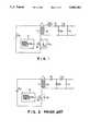
- FIG. 2A circuit diagram of a conventional forward DC-DC converter with one switching transistor is shown in FIG. 2, and the timings of voltage and current waveforms in this DC-DC converter are shown in FIG. 4.
- a DC source E sa primary winding L 1 of a transformer T 1 , and a transistor Q 1 that acts as a switching element form a series circuit, and a rectifying and smoothing circuit formed of a rectifier diode D 1 , a choke coil L 3 , a fly-wheel diode D 2 , and a smoothing capacitor C 1 is connected to a secondary winding L 2 of the transformer T 1 .
- the transistor Q 1receives a gate voltage from a control circuit that is not shown in the figure.
- FIG. 4shows the waveforms of the gate voltage V G1 of the transistor Q 1 , the drain-source voltage V Q1 of the transistor Q 1 , and the current I Q1 flowing through the transistor Q 1 via the primary winding L 1 , expressed against the same horizontal time axis.
- the drain-source voltage V Q1 and the current I Q1are superimposed during a period between a time t 1 at which the transistor Q 1 turns on and a subsequent time t 2 , and during a period between a time t 3 at which the transistor Q 1 turns off and a subsequent time t 4 . This superimposition causes switching losses.
- the object of the present inventionis to provide a DC-DC converter with one switching transistor designed to reduce losses.
- the present inventionrelates to a DC-DC converter comprising a DC power source, a primary winding of a transformer, and a switching element connected in series, whereby a DC output is extracted via a rectifier and smoothing circuit connected to a secondary winding of the transformer while the switching element is on.
- the DC-DC converteris characterized in that a capacitor is connected in parallel to the switching element, and a saturable reactor is connected between the secondary winding of the transformer and the rectifier diode.
- FIG. 1is a circuit diagram of an embodiment of the DC-DC converter of the present invention
- FIG. 2is a circuit diagram of a conventional DC-DC converter
- FIG. 3is a timing chart of currents and voltages in the DC-DC converter of the present invention
- FIG. 4is a timing chart of currents and voltages in the DC-DC converter of FIG. 2.
- the DC-DC converter with one switching transistor of FIG. 1comprises a series circuit of a DC source E S , a primary winding L 1 of a transformer T 1 , and an insulated-gate field-effect transistor Q 1 that acts as a switching element, with a rectifying and smoothing circuit formed of a rectifier diode D 1 , a choke coil L 3 , a fly-wheel diode D 2 , and a smoothing capacitor C 1 being connected to a secondary winding L 2 of the transformer T 1 .
- a capacitor C 3is connected in parallel to the transistor Q 1
- a saturable reactor L 4is connected between the rectifier diode D 1 of the rectifying circuit and the secondary winding L 2 , and electric power is transferred via the transformer T 1 while the transistor Q 1 is on, transistor Q 1 being applied a gate voltage from a signal generating circuit 2.
- FIG. 3shows the waveforms of a gate voltage V G1 and a drain-source voltage V Q1 of the transistor Q 1 , a current I Q1 flowing from the drain to the source of the transistor Q 1 , a current I D1 flowing through the rectifier diode D 1 , a current I D23 flowing through the fly-wheel diode D 2 , and a current I C23 that is the sum of currents flowing through the parasitic capacitor C 2 of the transistor Q 1 and the capacitor C 3 , expressed against the same horizontal time axis.
- the gate voltage V G1 of the transistor Q 1becomes zero and the transistor Q 1 turns off, whereupon the current I Q1 that was flowing from the primary winding L 1 of the transformer T 1 to the transistor Q 1 becomes zero.
- magnetizing current that was flowing through primary winding L 1 during on periodtends to flow continuously, owing to the reaction of primary winding L 1 .
- this currentflow through the parasitic capacitor C 2 of the transistor Q 1 and the capacitor C 3 connected parallel to the transistor Q 1 , and is figured I C23 (the sum of the currents flowing through the two capacitors) in FIG. 3. Therefore, the voltage between the two ends of the parasitic capacitor C 2 and the capacitor C 3 (in other words, the drain-source voltage V Q1 of the transistor Q 1 ) rises smoothly while charging the parasitic capacitor C 2 and the capacitor C 3 .
- Equation (1)The frequency f of this resonance is given by Equation (1), and the voltage between the ends of the capacitor C 3 (in other words, the drain-source voltage V Q1 of the transistor Q 1 ) changes corresponding to a sine waveform of resonance. ##EQU1##
- Equation (1)L 1 is the inductance of the primary winding L 1 , C 2 is the parasitic capacitance of the transistor Q 1 , and C 3 is the capacitance of the capacitor C 3 .
- the polarity point side of the secondary winding L 2 marked by the dot ( ⁇ ) in FIG. 1becomes positive, and, if the rectifier diode D 1 is connected directly to the secondary winding L 2 , the rectifier diode D 1 becomes conductive at the same time as the diode D 2 which has been conductive up to this point, and the secondary winding L 2 of the transformer T 1 is electrically short. For this reason, there is no longer any inductance in the primary winding L 1 and hence there is no longer a resonant component, so the resonance does not continue.
- the saturable reactor L 4is connected between the secondary winding L 2 and the rectifier diode D 1 , and the time at which the rectifier diode D 1 becomes conductive is delayed during the period is delayed during the period between the time when the polarity side of the secondary winding L 2 marked by the dot ( ⁇ ) in FIG. 1 became positive (the time t 7 ) and the time when saturable reactor L 4 is saturated.
- the secondary winding L 2 of the transformer T 1is still electrically opened, so the resonance continues and, at a time t 8 , the voltage between the ends of the capacitor C 3 (in other words, the drain-source voltage V Q1 ) becomes zero.
- the period said abovemust be made longer than the period between the time t 7 and the time t 8 .
- the control circuitoperates to turn on the transistor Q 1 at the time t 8 at which it detects that the voltage V Q1 has become zero. Note that the circuit that detects the state of the voltage V Q1 in this manner is not shown in FIG. 1.
- the current I C23 of the parasitic capacitor C 2 of the transistor Q 1 and the capacitor C 3is denoted by (+) when it flows from the primary winding L 1 through the parasitic capacitor C 2 and the capacitor C 3 , and by (-) when it flows in the opposite direction.
- the switching elementcould also be a bipolar transistor, and that the present invention can be applied to a wide variety of forward DC-DC converters, each having one switching transistor.
- a capacitoris connected in parallel to the switching element, and a saturable reactor is connected between the secondary winding of the transformer and the rectifier diode.
- the magnetizing currentflows through the capacitor connected in parallel to the switching element, ensuring that the voltage between the two ends of the switching element rises smoothly.
- the switching elementturns on, a resonance phenomenon continues, causing the voltage between the ends of the switching element to fall to zero.
Landscapes
- Engineering & Computer Science (AREA)
- Power Engineering (AREA)
- Dc-Dc Converters (AREA)
Abstract
Description
Claims (2)
Applications Claiming Priority (2)
| Application Number | Priority Date | Filing Date | Title |
|---|---|---|---|
| JP1-266616 | 1989-10-14 | ||
| JP1266616AJPH0734652B2 (en) | 1989-10-14 | 1989-10-14 | DC-DC converter |
Publications (1)
| Publication Number | Publication Date |
|---|---|
| US5086381Atrue US5086381A (en) | 1992-02-04 |
Family
ID=17433289
Family Applications (1)
| Application Number | Title | Priority Date | Filing Date |
|---|---|---|---|
| US07/594,030Expired - LifetimeUS5086381A (en) | 1989-10-14 | 1990-10-09 | DC-DC converter |
Country Status (2)
| Country | Link |
|---|---|
| US (1) | US5086381A (en) |
| JP (1) | JPH0734652B2 (en) |
Cited By (3)
| Publication number | Priority date | Publication date | Assignee | Title |
|---|---|---|---|---|
| US5349514A (en)* | 1991-11-01 | 1994-09-20 | Origin Electric Company, Limited | Reduced-resonant-current zero-voltage-switched forward converter using saturable inductor |
| US5673183A (en)* | 1993-12-01 | 1997-09-30 | Melcher, Ag | DC/DC converter for low output voltages |
| US10186985B1 (en)* | 2018-04-09 | 2019-01-22 | Flex Ltd. | Isolated FAI 2 converter with clamped voltage rectifier and synchronous rectified solution |
Citations (6)
| Publication number | Priority date | Publication date | Assignee | Title |
|---|---|---|---|---|
| US4318164A (en)* | 1979-03-15 | 1982-03-02 | Tokyo Shibaura Denki Kabushiki Kaisha | High frequency switching circuit having preselected parameters to reduce power dissipation therein |
| US4399376A (en)* | 1981-02-17 | 1983-08-16 | Tokyo Shibaura Denki Kabushiki Kaisha | High frequency switching circuit |
| US4788634A (en)* | 1987-06-22 | 1988-11-29 | Massachusetts Institute Of Technology | Resonant forward converter |
| US4857822A (en)* | 1987-09-23 | 1989-08-15 | Virginia Tech Intellectual Properties, Inc. | Zero-voltage-switched multi-resonant converters including the buck and forward type |
| US4931918A (en)* | 1988-07-29 | 1990-06-05 | Yokogawa Electric Corporation | Ringing choke converter |
| US4959765A (en)* | 1988-02-24 | 1990-09-25 | Agence Spatiale Europeenne | DC to DC converter using quasi-resonance |
Family Cites Families (4)
| Publication number | Priority date | Publication date | Assignee | Title |
|---|---|---|---|---|
| JPH0667187B2 (en)* | 1984-01-23 | 1994-08-24 | 株式会社日立製作所 | Magnetically controlled switching regulator |
| JPS60144788U (en)* | 1984-03-05 | 1985-09-26 | 横河電機株式会社 | DC/DC converter |
| JPS62131768A (en)* | 1985-11-30 | 1987-06-15 | Tokyo Electric Co Ltd | Power source device |
| JPS63194587U (en)* | 1987-06-01 | 1988-12-14 |
- 1989
- 1989-10-14JPJP1266616Apatent/JPH0734652B2/ennot_activeExpired - Fee Related
- 1990
- 1990-10-09USUS07/594,030patent/US5086381A/ennot_activeExpired - Lifetime
Patent Citations (6)
| Publication number | Priority date | Publication date | Assignee | Title |
|---|---|---|---|---|
| US4318164A (en)* | 1979-03-15 | 1982-03-02 | Tokyo Shibaura Denki Kabushiki Kaisha | High frequency switching circuit having preselected parameters to reduce power dissipation therein |
| US4399376A (en)* | 1981-02-17 | 1983-08-16 | Tokyo Shibaura Denki Kabushiki Kaisha | High frequency switching circuit |
| US4788634A (en)* | 1987-06-22 | 1988-11-29 | Massachusetts Institute Of Technology | Resonant forward converter |
| US4857822A (en)* | 1987-09-23 | 1989-08-15 | Virginia Tech Intellectual Properties, Inc. | Zero-voltage-switched multi-resonant converters including the buck and forward type |
| US4959765A (en)* | 1988-02-24 | 1990-09-25 | Agence Spatiale Europeenne | DC to DC converter using quasi-resonance |
| US4931918A (en)* | 1988-07-29 | 1990-06-05 | Yokogawa Electric Corporation | Ringing choke converter |
Cited By (3)
| Publication number | Priority date | Publication date | Assignee | Title |
|---|---|---|---|---|
| US5349514A (en)* | 1991-11-01 | 1994-09-20 | Origin Electric Company, Limited | Reduced-resonant-current zero-voltage-switched forward converter using saturable inductor |
| US5673183A (en)* | 1993-12-01 | 1997-09-30 | Melcher, Ag | DC/DC converter for low output voltages |
| US10186985B1 (en)* | 2018-04-09 | 2019-01-22 | Flex Ltd. | Isolated FAI 2 converter with clamped voltage rectifier and synchronous rectified solution |
Also Published As
| Publication number | Publication date |
|---|---|
| JPH03135367A (en) | 1991-06-10 |
| JPH0734652B2 (en) | 1995-04-12 |
Similar Documents
| Publication | Publication Date | Title |
|---|---|---|
| US20210242784A1 (en) | Flyback converter, control circuit and control method thereof | |
| US5734563A (en) | Synchronous rectification type converter | |
| US6483724B1 (en) | DC/DC ZVS full bridge converter power supply method and apparatus | |
| US5111372A (en) | DC-DC converter | |
| US6016258A (en) | Full bridge DC-DC converters | |
| US5508904A (en) | Switching regulator having superimposing chopping-wave voltage forming circuit | |
| US11070135B2 (en) | Converter with soft-start period of output voltage | |
| US10778218B2 (en) | Transformer based gate drive circuit | |
| US6487094B1 (en) | High efficiency DC-DC power converter | |
| JP3221185B2 (en) | Switching power supply | |
| US5640318A (en) | Forward converter for off-line applications | |
| US6477064B1 (en) | High efficiency DC-DC power converter with turn-off snubber | |
| US5801932A (en) | Interleaved current-fed forward converter | |
| US6437518B1 (en) | Lighting circuit for an electric discharge lamp | |
| US20070047267A1 (en) | Electric power converter | |
| JP2513381B2 (en) | Power supply circuit | |
| US5086381A (en) | DC-DC converter | |
| EP0058399B1 (en) | High frequency switching circuit | |
| US6704211B1 (en) | DC-to-DC converter | |
| TW202406280A (en) | Zvs assist snubber for switching converter | |
| US20020000923A1 (en) | Switching power supply circuit | |
| JP3022620B2 (en) | DC-DC converter | |
| US6008997A (en) | Series resonant converter with inherent short circuit protection | |
| US12283893B2 (en) | Converter circuit with half-bridge current-doubler rectifier and integrated magnetics | |
| KR100213671B1 (en) | A reducing ripple current circuit for dc/dc converter |
Legal Events
| Date | Code | Title | Description |
|---|---|---|---|
| AS | Assignment | Owner name:TOKO KABUSHIKI KAISHA, JAPAN Free format text:ASSIGNMENT OF ASSIGNORS INTEREST.;ASSIGNOR:NORIGOE, ISAMI;REEL/FRAME:005473/0253 Effective date:19901003 Owner name:YUTAKA ELECTRIC MFG. CO., LTD., JAPAN Free format text:ASSIGNMENT OF ASSIGNORS INTEREST.;ASSIGNOR:NORIGOE, ISAMI;REEL/FRAME:005473/0253 Effective date:19901003 Owner name:NEMIC LAMBDA KABUSHIKI KAISHA, JAPAN Free format text:ASSIGNMENT OF ASSIGNORS INTEREST.;ASSIGNORS:KAMEYAMA, SHIGERU;ARAKAWA, KOJI;WATANABE, KAZUSHI;AND OTHERS;REEL/FRAME:005473/0251 Effective date:19901003 Owner name:NEMIC LAMBDA KABUSHIKI KAISHA, JAPAN Free format text:ASSIGNMENT OF ASSIGNORS INTEREST.;ASSIGNOR:NORIGOE, ISAMI;REEL/FRAME:005473/0253 Effective date:19901003 Owner name:YUTAKA ELECTRIC MFG. CO., LTD., JAPAN Free format text:ASSIGNMENT OF ASSIGNORS INTEREST.;ASSIGNORS:KAMEYAMA, SHIGERU;ARAKAWA, KOJI;WATANABE, KAZUSHI;AND OTHERS;REEL/FRAME:005473/0251 Effective date:19901003 Owner name:TOKO KABUSHIKI KAISHA, JAPAN Free format text:ASSIGNMENT OF ASSIGNORS INTEREST.;ASSIGNORS:KAMEYAMA, SHIGERU;ARAKAWA, KOJI;WATANABE, KAZUSHI;AND OTHERS;REEL/FRAME:005473/0251 Effective date:19901003 Owner name:DENSETSU CORPORATION, JAPAN Free format text:ASSIGNMENT OF ASSIGNORS INTEREST.;ASSIGNOR:NORIGOE, ISAMI;REEL/FRAME:005473/0253 Effective date:19901003 Owner name:DENSETSU CORPORATION, JAPAN Free format text:ASSIGNMENT OF ASSIGNORS INTEREST.;ASSIGNORS:KAMEYAMA, SHIGERU;ARAKAWA, KOJI;WATANABE, KAZUSHI;AND OTHERS;REEL/FRAME:005473/0251 Effective date:19901003 | |
| STCF | Information on status: patent grant | Free format text:PATENTED CASE | |
| FPAY | Fee payment | Year of fee payment:4 | |
| FPAY | Fee payment | Year of fee payment:8 | |
| FPAY | Fee payment | Year of fee payment:12 | |
| AS | Assignment | Owner name:TDK-LAMBDA CORPORATION, JAPAN Free format text:CHANGE OF NAME;ASSIGNOR:NEMIC-LAMBDA K.K.;REEL/FRAME:022288/0161 Effective date:20090129 |