US5086014A - Schottky diode manufacturing process employing the synthesis of a polycrystalline diamond thin film - Google Patents
Schottky diode manufacturing process employing the synthesis of a polycrystalline diamond thin filmDownload PDFInfo
- Publication number
- US5086014A US5086014AUS07/584,110US58411090AUS5086014AUS 5086014 AUS5086014 AUS 5086014AUS 58411090 AUS58411090 AUS 58411090AUS 5086014 AUS5086014 AUS 5086014A
- Authority
- US
- United States
- Prior art keywords
- diamond film
- schottky diode
- substrate
- polycrystalline diamond
- type
- Prior art date
- Legal status (The legal status is an assumption and is not a legal conclusion. Google has not performed a legal analysis and makes no representation as to the accuracy of the status listed.)
- Expired - Lifetime
Links
- 239000010432diamondSubstances0.000titleclaimsabstractdescription40
- 229910003460diamondInorganic materials0.000titleclaimsabstractdescription40
- 238000004519manufacturing processMethods0.000titleclaimsabstractdescription12
- 230000015572biosynthetic processEffects0.000titleclaimsdescription8
- 238000003786synthesis reactionMethods0.000titleclaimsdescription6
- 239000010409thin filmSubstances0.000titleclaims2
- 239000000758substrateSubstances0.000claimsabstractdescription22
- 229910052751metalInorganic materials0.000claimsabstractdescription7
- 239000002184metalSubstances0.000claimsabstractdescription6
- 229910052719titaniumInorganic materials0.000claimsabstractdescription5
- 229910052721tungstenInorganic materials0.000claimsabstractdescription5
- 229910052782aluminiumInorganic materials0.000claimsabstract4
- ZOXJGFHDIHLPTG-UHFFFAOYSA-NBoronChemical compound[B]ZOXJGFHDIHLPTG-UHFFFAOYSA-N0.000claimsdescription5
- 229910052796boronInorganic materials0.000claimsdescription5
- 238000000034methodMethods0.000claimsdescription5
- 229910052737goldInorganic materials0.000claimsdescription4
- OKTJSMMVPCPJKN-UHFFFAOYSA-NCarbonChemical compound[C]OKTJSMMVPCPJKN-UHFFFAOYSA-N0.000claimsdescription3
- 229910052799carbonInorganic materials0.000claimsdescription3
- 230000008021depositionEffects0.000claimsdescription2
- 239000010408filmSubstances0.000claims7
- 229910052697platinumInorganic materials0.000claims3
- XUIMIQQOPSSXEZ-UHFFFAOYSA-NSiliconChemical compound[Si]XUIMIQQOPSSXEZ-UHFFFAOYSA-N0.000claims2
- 229910052710siliconInorganic materials0.000claims2
- 239000010703siliconSubstances0.000claims2
- 238000010438heat treatmentMethods0.000claims1
- 239000002245particleSubstances0.000claims1
- 238000005498polishingMethods0.000claims1
- 238000006243chemical reactionMethods0.000description4
- 238000005268plasma chemical vapour depositionMethods0.000description4
- 238000000151depositionMethods0.000description3
- 239000000203mixtureSubstances0.000description3
- 239000012808vapor phaseSubstances0.000description3
- 239000004065semiconductorSubstances0.000description2
- 229910001218Gallium arsenideInorganic materials0.000description1
- BQCADISMDOOEFD-UHFFFAOYSA-NSilverChemical compound[Ag]BQCADISMDOOEFD-UHFFFAOYSA-N0.000description1
- 229910002091carbon monoxideInorganic materials0.000description1
- 238000007796conventional methodMethods0.000description1
- ZOCHARZZJNPSEU-UHFFFAOYSA-NdiboronChemical compoundB#BZOCHARZZJNPSEU-UHFFFAOYSA-N0.000description1
- 230000000149penetrating effectEffects0.000description1
- 239000010453quartzSubstances0.000description1
- 230000005855radiationEffects0.000description1
- VYPSYNLAJGMNEJ-UHFFFAOYSA-Nsilicon dioxideInorganic materialsO=[Si]=OVYPSYNLAJGMNEJ-UHFFFAOYSA-N0.000description1
- 229910052709silverInorganic materials0.000description1
- 239000004332silverSubstances0.000description1
- 230000002194synthesizing effectEffects0.000description1
Images


Classifications
- H—ELECTRICITY
- H10—SEMICONDUCTOR DEVICES; ELECTRIC SOLID-STATE DEVICES NOT OTHERWISE PROVIDED FOR
- H10D—INORGANIC ELECTRIC SEMICONDUCTOR DEVICES
- H10D8/00—Diodes
- H10D8/60—Schottky-barrier diodes
- H—ELECTRICITY
- H01—ELECTRIC ELEMENTS
- H01L—SEMICONDUCTOR DEVICES NOT COVERED BY CLASS H10
- H01L21/00—Processes or apparatus adapted for the manufacture or treatment of semiconductor or solid state devices or of parts thereof
- H01L21/02—Manufacture or treatment of semiconductor devices or of parts thereof
- H01L21/02104—Forming layers
- H01L21/02365—Forming inorganic semiconducting materials on a substrate
- H01L21/02367—Substrates
- H01L21/0237—Materials
- H01L21/02373—Group 14 semiconducting materials
- H01L21/02381—Silicon, silicon germanium, germanium
- H—ELECTRICITY
- H01—ELECTRIC ELEMENTS
- H01L—SEMICONDUCTOR DEVICES NOT COVERED BY CLASS H10
- H01L21/00—Processes or apparatus adapted for the manufacture or treatment of semiconductor or solid state devices or of parts thereof
- H01L21/02—Manufacture or treatment of semiconductor devices or of parts thereof
- H01L21/02104—Forming layers
- H01L21/02365—Forming inorganic semiconducting materials on a substrate
- H01L21/02518—Deposited layers
- H01L21/02521—Materials
- H01L21/02524—Group 14 semiconducting materials
- H01L21/02527—Carbon, e.g. diamond-like carbon
- H—ELECTRICITY
- H01—ELECTRIC ELEMENTS
- H01L—SEMICONDUCTOR DEVICES NOT COVERED BY CLASS H10
- H01L21/00—Processes or apparatus adapted for the manufacture or treatment of semiconductor or solid state devices or of parts thereof
- H01L21/02—Manufacture or treatment of semiconductor devices or of parts thereof
- H01L21/02104—Forming layers
- H01L21/02365—Forming inorganic semiconducting materials on a substrate
- H01L21/02518—Deposited layers
- H01L21/0257—Doping during depositing
- H01L21/02573—Conductivity type
- H01L21/02579—P-type
- H—ELECTRICITY
- H01—ELECTRIC ELEMENTS
- H01L—SEMICONDUCTOR DEVICES NOT COVERED BY CLASS H10
- H01L21/00—Processes or apparatus adapted for the manufacture or treatment of semiconductor or solid state devices or of parts thereof
- H01L21/02—Manufacture or treatment of semiconductor devices or of parts thereof
- H01L21/02104—Forming layers
- H01L21/02365—Forming inorganic semiconducting materials on a substrate
- H01L21/02612—Formation types
- H01L21/02617—Deposition types
- H01L21/0262—Reduction or decomposition of gaseous compounds, e.g. CVD
- H—ELECTRICITY
- H01—ELECTRIC ELEMENTS
- H01L—SEMICONDUCTOR DEVICES NOT COVERED BY CLASS H10
- H01L21/00—Processes or apparatus adapted for the manufacture or treatment of semiconductor or solid state devices or of parts thereof
- H01L21/02—Manufacture or treatment of semiconductor devices or of parts thereof
- H01L21/04—Manufacture or treatment of semiconductor devices or of parts thereof the devices having potential barriers, e.g. a PN junction, depletion layer or carrier concentration layer
- H01L21/18—Manufacture or treatment of semiconductor devices or of parts thereof the devices having potential barriers, e.g. a PN junction, depletion layer or carrier concentration layer the devices having semiconductor bodies comprising elements of Group IV of the Periodic Table or AIIIBV compounds with or without impurities, e.g. doping materials
- H01L21/28—Manufacture of electrodes on semiconductor bodies using processes or apparatus not provided for in groups H01L21/20 - H01L21/268
- H01L21/283—Deposition of conductive or insulating materials for electrodes conducting electric current
- H01L21/285—Deposition of conductive or insulating materials for electrodes conducting electric current from a gas or vapour, e.g. condensation
- H01L21/28506—Deposition of conductive or insulating materials for electrodes conducting electric current from a gas or vapour, e.g. condensation of conductive layers
- H01L21/28512—Deposition of conductive or insulating materials for electrodes conducting electric current from a gas or vapour, e.g. condensation of conductive layers on semiconductor bodies comprising elements of Group IV of the Periodic Table
- H01L21/28537—Deposition of Schottky electrodes
- H—ELECTRICITY
- H10—SEMICONDUCTOR DEVICES; ELECTRIC SOLID-STATE DEVICES NOT OTHERWISE PROVIDED FOR
- H10D—INORGANIC ELECTRIC SEMICONDUCTOR DEVICES
- H10D62/00—Semiconductor bodies, or regions thereof, of devices having potential barriers
- H10D62/80—Semiconductor bodies, or regions thereof, of devices having potential barriers characterised by the materials
- H10D62/83—Semiconductor bodies, or regions thereof, of devices having potential barriers characterised by the materials being Group IV materials, e.g. B-doped Si or undoped Ge
- H10D62/8303—Diamond
- H—ELECTRICITY
- H10—SEMICONDUCTOR DEVICES; ELECTRIC SOLID-STATE DEVICES NOT OTHERWISE PROVIDED FOR
- H10D—INORGANIC ELECTRIC SEMICONDUCTOR DEVICES
- H10D64/00—Electrodes of devices having potential barriers
- H10D64/60—Electrodes characterised by their materials
- H10D64/62—Electrodes ohmically coupled to a semiconductor
- H—ELECTRICITY
- H10—SEMICONDUCTOR DEVICES; ELECTRIC SOLID-STATE DEVICES NOT OTHERWISE PROVIDED FOR
- H10D—INORGANIC ELECTRIC SEMICONDUCTOR DEVICES
- H10D8/00—Diodes
- H10D8/01—Manufacture or treatment
- H10D8/051—Manufacture or treatment of Schottky diodes
- H—ELECTRICITY
- H10—SEMICONDUCTOR DEVICES; ELECTRIC SOLID-STATE DEVICES NOT OTHERWISE PROVIDED FOR
- H10D—INORGANIC ELECTRIC SEMICONDUCTOR DEVICES
- H10D8/00—Diodes
- H10D8/30—Point-contact diodes
- Y—GENERAL TAGGING OF NEW TECHNOLOGICAL DEVELOPMENTS; GENERAL TAGGING OF CROSS-SECTIONAL TECHNOLOGIES SPANNING OVER SEVERAL SECTIONS OF THE IPC; TECHNICAL SUBJECTS COVERED BY FORMER USPC CROSS-REFERENCE ART COLLECTIONS [XRACs] AND DIGESTS
- Y10—TECHNICAL SUBJECTS COVERED BY FORMER USPC
- Y10S—TECHNICAL SUBJECTS COVERED BY FORMER USPC CROSS-REFERENCE ART COLLECTIONS [XRACs] AND DIGESTS
- Y10S148/00—Metal treatment
- Y10S148/14—Schottky barrier contacts
Definitions
- the present inventionrelates to a process of manufacturing electronic devices, particularly, Schottky diodes, employing vapor-phase diamond synthesis.
- a boron-doped (B-doped) p-type diamond filmis obtained by doping with boron, i.e., a metallic element of group III.
- B-doped p-type diamond filmsare expected to form Schottky diodes having excellent heat and radiation resistance, which has never been achieved by conventional Schottky diodes produced with Si and GaAs. It is also expected that other electronic devices having excellent characteristics can be fabricated using diamond films.
- a Schottky diodehas been reported, as shown in FIG. 6, in 1989-nen Shunki Oyo Butsuri Gakkai Yokoshu, 2a-N-7 No. 2.
- This Schottky diodeis formed by depositing a B-doped p-type polycrystalline diamond film a on a p-type Si substrate b (the diamond film was prepared using diborane (B 2 H 6 ) and a 5% CO gas diluted by H 2 ).
- an In electrode cwhich has an ohmic characteristic.
- An Al needle electrode dis placed on the B-doped p-type polycrystalline diamond film a.
- This point contact electrodeis a Schottky characteristic.
- this Schottky diodeprevents a flow of electric current when a positive voltage is applied to the Al needle electrode d, whereas it permits a flow of electric current, when a negative voltage is applied to the Al needle.
- the aforementioned paperalso reports that a device employing a p-type semiconductor diamond film deposited using a source gas of B 2 H 6 and a 0.5% CH 4 diluted by H 2 exhibits a current-to-voltage (I-V) characteristic as shown in FIG. 8 and does not have Schottky characteristics.
- I-Vcurrent-to-voltage
- This Schottky diodeis formed by depositing a polycrystalline diamond film a' on a p-type (100)Si substrate b' having a resistivity in the range of 0.01 to 0.1 ⁇ .cm (the diamond film was prepared by a microwave plasma CVD process using CH 4 diluted by H 2 as a source gas).
- An ohmic contact electrode c'is attached on the backside of the substrate, and an Au electrode d' of a diameter of 0.1 cm and a thickness in the range of 140 to 500 ⁇ is deposited on the polycrystalline diamond film a'.
- the I-V characteristicis shown in FIG. 10.
- the present inventionhas developed as a Schottky diode having excellent characteristics by applying polycrystalline diamond film synthesis techniques in addition to the prior art. It has been found that a satisfactory Schottky diode can be produced using a B-doped diamond film synthesized by a B 2 H 4 -CH 4 -H 2 gas mixture when the B 2 H 4 concentration in the gas mixture is within a certain range, as described below:
- a Schottky diode manufacturing process using a polycrystalline diamond filmcomprises: a deposition of a B-doped p-type polycrystalline diamond film on a low-resistance p-type Si substrate by using a source gas consisting of CH 4 , H 2 and B 2 H 6 and having a boron/carbon concentration ratio greater than 0.01 ppm and less than 20 ppm; a formation of an ohmic contact on the p-type Si substrate; and a formation a metal electrode of Al Pt, Au, Ti or W on the diamond film.
- the Schottky diodeWhen the B/C concentration ratio is 20 ppm or higher, the Schottky diode has rather an ohmic I-V characteristic and has no rectifying property. When the B/C concentration ratio is less than 0.01 ppm, the carrier density is on the order of 10 15 /cm 2 , and hence the diamond film does not have the characteristics of p-type semiconductor.
- the p-type polycrystalline diamond film formed by the conventional techniques using a CH 4 gas as a source gasdid not exhibit Schottky characteristics because of an excessively high B/C concentration ratio of the source gas.
- FIG. 1is a schematic view of a vapor-phase diamond synthesizing apparatus employed for carrying out a Schottky diode manufacturing process embodying the present invention
- FIG. 2is a cross sectional view of an example of a Schottky diode manufactured by the Schottky diode manufacturing process in accordance with the present invention
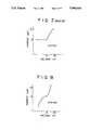
- FIG. 3is a graph showing the I-V characteristic of the Schottky diode of FIG. 2;
- FIG. 4is a graph showing the I-V characteristic of a Schottky diode as a control
- FIG. 5is a cross sectional view of another Schottky diode manufactured by the Schottky diode manufacturing process in accordance with the present invention.
- FIG. 6is a cross sectional view of a conventional Schottky diode
- FIG. 7is a graph showing the I-V characteristic of the Schottky diode of FIG. 6;
- FIG. 8is a graph showing the I-V characteristic of a conventional Schottky diode for comparison
- FIG. 9is a cross sectional view of another conventional Schottky diode.
- FIG. 10is a graph showing the I-V characteristic of the Schottky diode of FIG. 9.
- a Schottky diode manufacturing process in accordance with the present inventionis carried out, by way of example, by a microwave plasma CVD apparatus shown in FIG. 1.
- the microwave generated by a microwave power source 1is transferred through an isolator 2, a power monitor 3 and a tuner 4 and a waveguide 5 into a reaction chamber 6 defined by a quartz tube penetrating perpendicularly through the waveguide 5.
- a substrate 7is placed within the reaction chamber 6 at the intersection of the waveguide and the reaction chamber 6.
- a CH 4 -H 2 gas mixtureis introduced into the reaction chamber 6 and the microwave is applied to the CH 4 -H 2 gas to generate a plasma around the substrate 7, whereby a polycrystalline diamond film is formed on the substrate 7.
- a Schottky diodewas manufactured by the Schottky diode manufacturing method of the present invention.
- a low-resistance p-type Si wafer with a resistivity in the range of 1 to 10 ⁇ .cmwas buff-polished for one hour using a 0.25 ⁇ m diamond paste.
- a substrate 7 of 20 mm ⁇ 10 mmwas then cut out from the polished wafer.
- a microwave plasma CVD apparatus as shown in FIG. 1was used to deposit a polycrystalline diamond film on the substrate 7.
- a source gas of 0.5% CH 4 -H 2 containing B 2 H 6 (the B/C ratio was 2 ppm)was used.
- the experimental conditions of the microwave plasma CVDwere: the gas flow rate: 100 cc/min the pressure: 31.5 torr, strate temperature: 800° C., and the processing time: 7 hr.
- p-type polycrystalline diamond film 8 of 2 ⁇ m thickwas formed on the substrate 7 as shown in FIG. 2.
- the measured I-V characteristic of the Schottky diodeis shown in FIG. 3.
- the Schottky diodeprevented the flow of electric current when positive voltage is applied to the Al needle electrode 10 and permitted current to flow when negative voltage is applied to the Al needle electrode 10.
- the Schottky characteristic of the Schottky diodewas found to be satisfactory.
- a Schottky diode manufactured as a control by using a source gas containing B 2 H 6 of a B/C ratio greater than 20 ppmdid not have Schottky characteristic as shown in FIG. 4.
- the Schottky diode of the present inventionmay be provided with an Al planar electrode 11 as shown in FIG. 5 instead of the Al needle electrode 10 shown in FIG. 2.
Landscapes
- Engineering & Computer Science (AREA)
- Physics & Mathematics (AREA)
- Condensed Matter Physics & Semiconductors (AREA)
- General Physics & Mathematics (AREA)
- Manufacturing & Machinery (AREA)
- Computer Hardware Design (AREA)
- Microelectronics & Electronic Packaging (AREA)
- Power Engineering (AREA)
- Chemical & Material Sciences (AREA)
- Materials Engineering (AREA)
- Electrodes Of Semiconductors (AREA)
Abstract
Description
1. Field of the Invention
The present invention relates to a process of manufacturing electronic devices, particularly, Schottky diodes, employing vapor-phase diamond synthesis.
2. Description of the Prior Art
In forming a diamond film through vapor-phase synthesis, a boron-doped (B-doped) p-type diamond film is obtained by doping with boron, i.e., a metallic element of group III. B-doped p-type diamond films are expected to form Schottky diodes having excellent heat and radiation resistance, which has never been achieved by conventional Schottky diodes produced with Si and GaAs. It is also expected that other electronic devices having excellent characteristics can be fabricated using diamond films.
A Schottky diode has been reported, as shown in FIG. 6, in 1989-nen Shunki Oyo Butsuri Gakkai Yokoshu, 2a-N-7 No. 2. This Schottky diode is formed by depositing a B-doped p-type polycrystalline diamond film a on a p-type Si substrate b (the diamond film was prepared using diborane (B2 H6) and a 5% CO gas diluted by H2). On the back side of the Si substrate, an In electrode c which has an ohmic characteristic. An Al needle electrode d is placed on the B-doped p-type polycrystalline diamond film a. This point contact electrode is a Schottky characteristic. As shown in FIG. 7, this Schottky diode prevents a flow of electric current when a positive voltage is applied to the Al needle electrode d, whereas it permits a flow of electric current, when a negative voltage is applied to the Al needle.
The aforementioned paper also reports that a device employing a p-type semiconductor diamond film deposited using a source gas of B2 H6 and a 0.5% CH4 diluted by H2 exhibits a current-to-voltage (I-V) characteristic as shown in FIG. 8 and does not have Schottky characteristics.
A study of a Schottky diode shown in FIG. 9 has been reported in Journal of Applied Physics, Vol. 65, No. 5, pp. 2139-2414 (1989). This Schottky diode is formed by depositing a polycrystalline diamond film a' on a p-type (100)Si substrate b' having a resistivity in the range of 0.01 to 0.1 Ω.cm (the diamond film was prepared by a microwave plasma CVD process using CH4 diluted by H2 as a source gas). An ohmic contact electrode c' is attached on the backside of the substrate, and an Au electrode d' of a diameter of 0.1 cm and a thickness in the range of 140 to 500 Å is deposited on the polycrystalline diamond film a'. The I-V characteristic is shown in FIG. 10.
The present invention has developed as a Schottky diode having excellent characteristics by applying polycrystalline diamond film synthesis techniques in addition to the prior art. It has been found that a satisfactory Schottky diode can be produced using a B-doped diamond film synthesized by a B2 H4 -CH4 -H2 gas mixture when the B2 H4 concentration in the gas mixture is within a certain range, as described below:
In one aspect of the present invention, a Schottky diode manufacturing process using a polycrystalline diamond film comprises: a deposition of a B-doped p-type polycrystalline diamond film on a low-resistance p-type Si substrate by using a source gas consisting of CH4, H2 and B2 H6 and having a boron/carbon concentration ratio greater than 0.01 ppm and less than 20 ppm; a formation of an ohmic contact on the p-type Si substrate; and a formation a metal electrode of Al Pt, Au, Ti or W on the diamond film.
When the B/C concentration ratio is 20 ppm or higher, the Schottky diode has rather an ohmic I-V characteristic and has no rectifying property. When the B/C concentration ratio is less than 0.01 ppm, the carrier density is on the order of 1015 /cm2, and hence the diamond film does not have the characteristics of p-type semiconductor.
It is inferred from FIG. 8 that the p-type polycrystalline diamond film formed by the conventional techniques using a CH4 gas as a source gas did not exhibit Schottky characteristics because of an excessively high B/C concentration ratio of the source gas.
The above and other objects, features and advantages of the present invention will become more apparent form the following description taken in connection with the accompanying drawings in which:
FIG. 1 is a schematic view of a vapor-phase diamond synthesizing apparatus employed for carrying out a Schottky diode manufacturing process embodying the present invention;
FIG. 2 is a cross sectional view of an example of a Schottky diode manufactured by the Schottky diode manufacturing process in accordance with the present invention;
FIG. 3 is a graph showing the I-V characteristic of the Schottky diode of FIG. 2;
FIG. 4 is a graph showing the I-V characteristic of a Schottky diode as a control;
FIG. 5 is a cross sectional view of another Schottky diode manufactured by the Schottky diode manufacturing process in accordance with the present invention;
FIG. 6 is a cross sectional view of a conventional Schottky diode;
FIG. 7 is a graph showing the I-V characteristic of the Schottky diode of FIG. 6;
FIG. 8 is a graph showing the I-V characteristic of a conventional Schottky diode for comparison;
FIG. 9 is a cross sectional view of another conventional Schottky diode; and
FIG. 10 is a graph showing the I-V characteristic of the Schottky diode of FIG. 9.
A Schottky diode manufacturing process in accordance with the present invention is carried out, by way of example, by a microwave plasma CVD apparatus shown in FIG. 1. In this apparatus, the microwave generated by amicrowave power source 1 is transferred through anisolator 2, apower monitor 3 and atuner 4 and awaveguide 5 into areaction chamber 6 defined by a quartz tube penetrating perpendicularly through thewaveguide 5. Asubstrate 7 is placed within thereaction chamber 6 at the intersection of the waveguide and thereaction chamber 6. A CH4 -H2 gas mixture is introduced into thereaction chamber 6 and the microwave is applied to the CH4 -H2 gas to generate a plasma around thesubstrate 7, whereby a polycrystalline diamond film is formed on thesubstrate 7.
A Schottky diode was manufactured by the Schottky diode manufacturing method of the present invention.
(i) A low-resistance p-type Si wafer with a resistivity in the range of 1 to 10 Ω.cm was buff-polished for one hour using a 0.25 μm diamond paste. Asubstrate 7 of 20 mm×10 mm was then cut out from the polished wafer.
(ii) A microwave plasma CVD apparatus as shown in FIG. 1 was used to deposit a polycrystalline diamond film on thesubstrate 7.
A source gas of 0.5% CH4 -H2 containing B2 H6 (the B/C ratio was 2 ppm) was used. The experimental conditions of the microwave plasma CVD were: the gas flow rate: 100 cc/min the pressure: 31.5 torr, strate temperature: 800° C., and the processing time: 7 hr.
As a result, p-typepolycrystalline diamond film 8 of 2 μm thick was formed on thesubstrate 7 as shown in FIG. 2.
(iii) A 3 mm square chip was cut out from thesubstrate 7 which was coated by a p-typepolycrystalline diamond film 8. Anohmic contact 9 was formed on the backside of the low-resistance p-type Si substrate 7 by a silver paste, and a Schottky contact was formed on thediamond film 8 by attaching anAl needle electrode 10.
(iv) The measured I-V characteristic of the Schottky diode is shown in FIG. 3. The Schottky diode prevented the flow of electric current when positive voltage is applied to theAl needle electrode 10 and permitted current to flow when negative voltage is applied to theAl needle electrode 10. The Schottky characteristic of the Schottky diode was found to be satisfactory.
A Schottky diode manufactured as a control by using a source gas containing B2 H6 of a B/C ratio greater than 20 ppm did not have Schottky characteristic as shown in FIG. 4.
The Schottky diode of the present invention may be provided with an Al planar electrode 11 as shown in FIG. 5 instead of theAl needle electrode 10 shown in FIG. 2.
Although the invention has been described in its preferred form with a certain degree of particularity, obviously many changes and variations are possible therein. It is therefore to be understood that the present invention may be practiced otherwise than as specifically described herein without departing from the scope and spirit thereof.
Claims (5)
1. A Schottky diode manufacturing process employing the synthesis of a polycrystalline diamond film, comprising: a deposition of a B-doped p-type polycrystalline diamond film on a low-resistance p-type Si substrate by using a source gas consisting of CH4, H2 and B2 H6 and having boron/carbon concentration ratio greater than 0.01 ppm and less than 20 ppm; forming an ohmic contact on the back of the p-type Si substrate; and forming a metal electrode on the B-doped p-type polycrystalline diamond thin film.
2. A Schottky diode manufacturing process according to claim 1, wherein the metal electrode is formed of a metal chosen from the group consisting of Al, Pt, Au, Ti and W.
3. A Schottky diode manufacturing process employing the synthesis of a polycrystalline diamond film, comprising the steps of:
polishing a surface of a p type silicon substrate with a diamond grit having submicron diamond particles;
placing said substrate in a CVD system;
heating said substrate to 800° C.;
flowing gas consisting of CH4, H2 and B2 H6 through said CVD system, wherein CH4 gas constitutes 0.5 percent of the flowing gas, the ratio of boron to carbon in said gas being between 0.01 and 20, to one million, the gas flow rate being sufficient to maintain the pressure in the system at 31.5 Torr;
igniting a microwave plasma in said CVD chamber;
growing a boron doped diamond film on said surface, for several hours;
forming an ohmic contact on the uncoated surface of said silicon substrate; and
forming a Schottky contact upon said diamond film.
4. A process according to claim 3, wherein said Schottky contact is formed by contacting a needle electrode tip to said diamond film, wherein said needle is formed from an element chosen from the group consisting of Al, Pt, Au, Ti and W.
5. A process according to claim 3, wherein said Schottky contact is formed by preparing a planar electrode on said diamond film, wherein said electrode is formed from a metal chosen from the group consisting of Al, Pt, Au, Ti and W.
Applications Claiming Priority (2)
| Application Number | Priority Date | Filing Date | Title |
|---|---|---|---|
| JP1-244399 | 1989-09-19 | ||
| JP1244399AJPH03105974A (en) | 1989-09-19 | 1989-09-19 | Manufacture of schottky diode by synthesizing polycrystalline diamond thin film |
Publications (1)
| Publication Number | Publication Date |
|---|---|
| US5086014Atrue US5086014A (en) | 1992-02-04 |
Family
ID=17118094
Family Applications (1)
| Application Number | Title | Priority Date | Filing Date |
|---|---|---|---|
| US07/584,110Expired - LifetimeUS5086014A (en) | 1989-09-19 | 1990-09-18 | Schottky diode manufacturing process employing the synthesis of a polycrystalline diamond thin film |
Country Status (3)
| Country | Link |
|---|---|
| US (1) | US5086014A (en) |
| JP (1) | JPH03105974A (en) |
| GB (1) | GB2236902B (en) |
Cited By (44)
| Publication number | Priority date | Publication date | Assignee | Title |
|---|---|---|---|---|
| US5285084A (en)* | 1992-09-02 | 1994-02-08 | Kobe Steel Usa | Diamond schottky diodes and gas sensors fabricated therefrom |
| US5300188A (en)* | 1992-11-13 | 1994-04-05 | Kobe Development Corp. | Process for making substantially smooth diamond |
| US5309000A (en)* | 1992-04-23 | 1994-05-03 | Kabushiki Kaisha Kobe Seiko Sho | Diamond films with heat-resisting ohmic electrodes |
| US5352908A (en)* | 1991-03-29 | 1994-10-04 | Kabushiki Kaisha Kobe Seiko Sho | Diamond Schottky diode with oxygen |
| US5353737A (en)* | 1992-04-16 | 1994-10-11 | Kabushiki Kaisha Kobe Seiko Sho | Method for forming boron-doped semiconducting diamond films |
| US5362975A (en)* | 1992-09-02 | 1994-11-08 | Kobe Steel Usa | Diamond-based chemical sensors |
| US5371383A (en)* | 1993-05-14 | 1994-12-06 | Kobe Steel Usa Inc. | Highly oriented diamond film field-effect transistor |
| US5399247A (en)* | 1993-12-22 | 1995-03-21 | Eastman Kodak Company | Method of electrolysis employing a doped diamond anode to oxidize solutes in wastewater |
| US5424561A (en)* | 1993-05-14 | 1995-06-13 | Kobe Steel Usa Inc. | Magnetic sensor element using highly-oriented diamond film and magnetic detector |
| US5442199A (en)* | 1993-05-14 | 1995-08-15 | Kobe Steel Usa, Inc. | Diamond hetero-junction rectifying element |
| US5491348A (en)* | 1993-05-14 | 1996-02-13 | Kobe Steel Usa, Inc. | Highly-oriented diamond film field-effect transistor |
| US5493131A (en)* | 1993-05-14 | 1996-02-20 | Kobe Steel Usa, Inc. | Diamond rectifying element |
| US5512873A (en)* | 1993-05-04 | 1996-04-30 | Saito; Kimitsugu | Highly-oriented diamond film thermistor |
| US5523160A (en)* | 1993-05-14 | 1996-06-04 | Kobe Steel Usa, Inc. | Highly-oriented diamond film |
| US5597762A (en)* | 1994-09-27 | 1997-01-28 | Nonophase Diamond Technologies, Inc. | Field-enhanced diffusion using optical activation |
| US5653952A (en)* | 1991-12-18 | 1997-08-05 | Kabushiki Kaisha Kobe Seiko Sho | Process for synthesizing diamond using combustion method |
| US5803967A (en)* | 1995-05-31 | 1998-09-08 | Kobe Steel Usa Inc. | Method of forming diamond devices having textured and highly oriented diamond layers therein |
| US6423384B1 (en) | 1999-06-25 | 2002-07-23 | Applied Materials, Inc. | HDP-CVD deposition of low dielectric constant amorphous carbon film |
| US6448184B1 (en) | 1998-06-25 | 2002-09-10 | Pacific Western Systems | Formation of diamond particle interconnects |
| US6610999B2 (en)* | 1998-04-06 | 2003-08-26 | California Institute Of Technology | Multiple stage high power diode |
| US6635583B2 (en) | 1998-10-01 | 2003-10-21 | Applied Materials, Inc. | Silicon carbide deposition for use as a low-dielectric constant anti-reflective coating |
| US20040067308A1 (en)* | 2002-10-07 | 2004-04-08 | Applied Materials, Inc. | Two-layer film for next generation damascene barrier application with good oxidation resistance |
| US6790788B2 (en) | 2003-01-13 | 2004-09-14 | Applied Materials Inc. | Method of improving stability in low k barrier layers |
| US6794311B2 (en) | 2000-07-14 | 2004-09-21 | Applied Materials Inc. | Method and apparatus for treating low k dielectric layers to reduce diffusion |
| US6838393B2 (en) | 2001-12-14 | 2005-01-04 | Applied Materials, Inc. | Method for producing semiconductor including forming a layer containing at least silicon carbide and forming a second layer containing at least silicon oxygen carbide |
| US20050042889A1 (en)* | 2001-12-14 | 2005-02-24 | Albert Lee | Bi-layer approach for a hermetic low dielectric constant layer for barrier applications |
| US20050101154A1 (en)* | 1999-06-18 | 2005-05-12 | Judy Huang | Plasma treatment to enhance adhesion and to minimize oxidation of carbon-containing layers |
| DE102004006544B3 (en)* | 2004-02-10 | 2005-09-08 | Infineon Technologies Ag | A method of depositing a conductive carbon material on a semiconductor to form a Schottky contact and semiconductor contact device |
| US20050202685A1 (en)* | 2004-03-15 | 2005-09-15 | Applied Materials, Inc. | Adhesion improvement for low k dielectrics |
| US20050233555A1 (en)* | 2004-04-19 | 2005-10-20 | Nagarajan Rajagopalan | Adhesion improvement for low k dielectrics to conductive materials |
| US20050233576A1 (en)* | 2001-12-14 | 2005-10-20 | Lee Ju-Hyung | Method of depositing dielectric materials in damascene applications |
| US6974766B1 (en) | 1998-10-01 | 2005-12-13 | Applied Materials, Inc. | In situ deposition of a low κ dielectric layer, barrier layer, etch stop, and anti-reflective coating for damascene application |
| US20050277302A1 (en)* | 2004-05-28 | 2005-12-15 | Nguyen Son V | Advanced low dielectric constant barrier layers |
| US20060006140A1 (en)* | 2004-07-09 | 2006-01-12 | Annamalai Lakshmanan | Hermetic low dielectric constant layer for barrier applications |
| US20060046479A1 (en)* | 2004-04-19 | 2006-03-02 | Applied Materials, Inc. | Adhesion improvement for low k dielectrics to conductive materials |
| US20060052752A1 (en)* | 2004-09-09 | 2006-03-09 | Kimberly-Clark Worldwide, Inc. | Artificial stoma and method of use |
| WO2006027669A1 (en)* | 2004-09-10 | 2006-03-16 | Element Six Limited | Switching device |
| US20060086850A1 (en)* | 2004-06-30 | 2006-04-27 | Cohen Douglas J | Lifting lid crusher |
| US20080070162A1 (en)* | 2006-08-25 | 2008-03-20 | Klaus-Dieter Ufert | Information storage elements and methods of manufacture thereof |
| US20080099827A1 (en)* | 2006-10-27 | 2008-05-01 | Franz Kreupl | Modifiable gate stack memory element |
| US20090201715A1 (en)* | 2008-02-11 | 2009-08-13 | Franz Kreupl | Carbon Diode Array for Resistivity Changing Memories |
| US7894253B2 (en) | 2006-10-27 | 2011-02-22 | Qimonda Ag | Carbon filament memory and fabrication method |
| RU2488912C2 (en)* | 2011-07-07 | 2013-07-27 | Российская Федерация, от имени которой выступает Министерство промышленности и торговли РФ | Method to manufacture schottky diode |
| CN104638026A (en)* | 2015-02-05 | 2015-05-20 | 西南科技大学 | Diamond schottky barrier diode and preparing method thereof |
Families Citing this family (3)
| Publication number | Priority date | Publication date | Assignee | Title |
|---|---|---|---|---|
| US5173761A (en)* | 1991-01-28 | 1992-12-22 | Kobe Steel Usa Inc., Electronic Materials Center | Semiconducting polycrystalline diamond electronic devices employing an insulating diamond layer |
| JPH05891A (en)* | 1991-06-21 | 1993-01-08 | Canon Inc | Diamond-metal bonded body |
| US5382808A (en)* | 1993-05-14 | 1995-01-17 | Kobe Steel, Usa Inc. | Metal boride ohmic contact on diamond and method for making same |
Citations (1)
| Publication number | Priority date | Publication date | Assignee | Title |
|---|---|---|---|---|
| US4925701A (en)* | 1988-05-27 | 1990-05-15 | Xerox Corporation | Processes for the preparation of polycrystalline diamond films |
Family Cites Families (1)
| Publication number | Priority date | Publication date | Assignee | Title |
|---|---|---|---|---|
| JP2584642B2 (en)* | 1987-12-17 | 1997-02-26 | 出光石油化学株式会社 | Schottky diode and method of manufacturing the same |
- 1989
- 1989-09-19JPJP1244399Apatent/JPH03105974A/enactivePending
- 1990
- 1990-09-18USUS07/584,110patent/US5086014A/ennot_activeExpired - Lifetime
- 1990-09-18GBGB9020362Apatent/GB2236902B/ennot_activeExpired - Fee Related
Patent Citations (1)
| Publication number | Priority date | Publication date | Assignee | Title |
|---|---|---|---|---|
| US4925701A (en)* | 1988-05-27 | 1990-05-15 | Xerox Corporation | Processes for the preparation of polycrystalline diamond films |
Non-Patent Citations (12)
| Title |
|---|
| Bazhenov et al., "Synthetic Diamons in Electronics (review)", Sov. Phys. Semicond., vol. 19, No. 8, Aug. 1985, pp. 829-841. |
| Bazhenov et al., Synthetic Diamons in Electronics (review) , Sov. Phys. Semicond., vol. 19, No. 8, Aug. 1985, pp. 829 841.* |
| Fujimori et al., "Characterization of Conducting Diamond Films", Vacuum, vol. 36, Nos. 1-3, 1986, pp. 99-102. |
| Fujimori et al., Characterization of Conducting Diamond Films , Vacuum, vol. 36, Nos. 1 3, 1986, pp. 99 102.* |
| Geis et al., "High-Temperature Point-Contact Transistors and Schottky Diodes Formed on Synthetic Boron-Doped Diamond", IEEE Electron Device Letters, vol. EDL-8, No. 8, Aug. 1987, pp. 341-343. |
| Geis et al., High Temperature Point Contact Transistors and Schottky Diodes Formed on Synthetic Boron Doped Diamond , IEEE Electron Device Letters, vol. EDL 8, No. 8, Aug. 1987, pp. 341 343.* |
| Glover, "The C-V Characteristics of Schottky Barriers on Laboratory Grown Semiconducting Diamonds", Solid State Electronics, 1973, vol. 16, pp. 973-983. |
| Glover, The C V Characteristics of Schottky Barriers on Laboratory Grown Semiconducting Diamonds , Solid State Electronics, 1973, vol. 16, pp. 973 983.* |
| Moazed et al., "Ohmic Contacts to Semiconducting Diamond", Appl. Phys. Lett., vol. 41, No. 10, p. 950, 1982. |
| Moazed et al., Ohmic Contacts to Semiconducting Diamond , Appl. Phys. Lett., vol. 41, No. 10, p. 950, 1982.* |
| Sze, Physics of Semiconductor Devices, Bell Labs, Inc., 1981, pp. 305 307.* |
| Sze, Physics of Semiconductor Devices, Bell Labs, Inc., 1981, pp. 305-307. |
Cited By (69)
| Publication number | Priority date | Publication date | Assignee | Title |
|---|---|---|---|---|
| US5352908A (en)* | 1991-03-29 | 1994-10-04 | Kabushiki Kaisha Kobe Seiko Sho | Diamond Schottky diode with oxygen |
| US5653952A (en)* | 1991-12-18 | 1997-08-05 | Kabushiki Kaisha Kobe Seiko Sho | Process for synthesizing diamond using combustion method |
| US5353737A (en)* | 1992-04-16 | 1994-10-11 | Kabushiki Kaisha Kobe Seiko Sho | Method for forming boron-doped semiconducting diamond films |
| US5309000A (en)* | 1992-04-23 | 1994-05-03 | Kabushiki Kaisha Kobe Seiko Sho | Diamond films with heat-resisting ohmic electrodes |
| US5362975A (en)* | 1992-09-02 | 1994-11-08 | Kobe Steel Usa | Diamond-based chemical sensors |
| US5285084A (en)* | 1992-09-02 | 1994-02-08 | Kobe Steel Usa | Diamond schottky diodes and gas sensors fabricated therefrom |
| US5300188A (en)* | 1992-11-13 | 1994-04-05 | Kobe Development Corp. | Process for making substantially smooth diamond |
| US5512873A (en)* | 1993-05-04 | 1996-04-30 | Saito; Kimitsugu | Highly-oriented diamond film thermistor |
| US5371383A (en)* | 1993-05-14 | 1994-12-06 | Kobe Steel Usa Inc. | Highly oriented diamond film field-effect transistor |
| US5442199A (en)* | 1993-05-14 | 1995-08-15 | Kobe Steel Usa, Inc. | Diamond hetero-junction rectifying element |
| US5491348A (en)* | 1993-05-14 | 1996-02-13 | Kobe Steel Usa, Inc. | Highly-oriented diamond film field-effect transistor |
| US5493131A (en)* | 1993-05-14 | 1996-02-20 | Kobe Steel Usa, Inc. | Diamond rectifying element |
| US5424561A (en)* | 1993-05-14 | 1995-06-13 | Kobe Steel Usa Inc. | Magnetic sensor element using highly-oriented diamond film and magnetic detector |
| US5523160A (en)* | 1993-05-14 | 1996-06-04 | Kobe Steel Usa, Inc. | Highly-oriented diamond film |
| US5399247A (en)* | 1993-12-22 | 1995-03-21 | Eastman Kodak Company | Method of electrolysis employing a doped diamond anode to oxidize solutes in wastewater |
| US5597762A (en)* | 1994-09-27 | 1997-01-28 | Nonophase Diamond Technologies, Inc. | Field-enhanced diffusion using optical activation |
| US5803967A (en)* | 1995-05-31 | 1998-09-08 | Kobe Steel Usa Inc. | Method of forming diamond devices having textured and highly oriented diamond layers therein |
| US6610999B2 (en)* | 1998-04-06 | 2003-08-26 | California Institute Of Technology | Multiple stage high power diode |
| US6448184B1 (en) | 1998-06-25 | 2002-09-10 | Pacific Western Systems | Formation of diamond particle interconnects |
| US20090130837A1 (en)* | 1998-10-01 | 2009-05-21 | Applied Materials, Inc. | In situ deposition of a low k dielectric layer, barrier layer, etch stop, and anti-reflective coating for damascene application |
| US6635583B2 (en) | 1998-10-01 | 2003-10-21 | Applied Materials, Inc. | Silicon carbide deposition for use as a low-dielectric constant anti-reflective coating |
| US7670945B2 (en) | 1998-10-01 | 2010-03-02 | Applied Materials, Inc. | In situ deposition of a low κ dielectric layer, barrier layer, etch stop, and anti-reflective coating for damascene application |
| US7470611B2 (en) | 1998-10-01 | 2008-12-30 | Applied Materials, Inc. | In situ deposition of a low K dielectric layer, barrier layer, etch stop, and anti-reflective coating for damascene application |
| US20060089007A1 (en)* | 1998-10-01 | 2006-04-27 | Applied Materials, Inc. | In situ deposition of a low K dielectric layer, barrier layer, etch stop, and anti-reflective coating for damascene application |
| US6974766B1 (en) | 1998-10-01 | 2005-12-13 | Applied Materials, Inc. | In situ deposition of a low κ dielectric layer, barrier layer, etch stop, and anti-reflective coating for damascene application |
| US20050181623A1 (en)* | 1998-10-01 | 2005-08-18 | Applied Materials, Inc. | Silicon carbide deposition for use as a low dielectric constant anti-reflective coating |
| US6951826B2 (en) | 1998-10-01 | 2005-10-04 | Applied Materials, Inc. | Silicon carbide deposition for use as a low dielectric constant anti-reflective coating |
| US7144606B2 (en) | 1999-06-18 | 2006-12-05 | Applied Materials, Inc. | Plasma treatment to enhance adhesion and to minimize oxidation of carbon-containing layers |
| US20050101154A1 (en)* | 1999-06-18 | 2005-05-12 | Judy Huang | Plasma treatment to enhance adhesion and to minimize oxidation of carbon-containing layers |
| US6423384B1 (en) | 1999-06-25 | 2002-07-23 | Applied Materials, Inc. | HDP-CVD deposition of low dielectric constant amorphous carbon film |
| US6794311B2 (en) | 2000-07-14 | 2004-09-21 | Applied Materials Inc. | Method and apparatus for treating low k dielectric layers to reduce diffusion |
| US20050233576A1 (en)* | 2001-12-14 | 2005-10-20 | Lee Ju-Hyung | Method of depositing dielectric materials in damascene applications |
| US6838393B2 (en) | 2001-12-14 | 2005-01-04 | Applied Materials, Inc. | Method for producing semiconductor including forming a layer containing at least silicon carbide and forming a second layer containing at least silicon oxygen carbide |
| US20050042889A1 (en)* | 2001-12-14 | 2005-02-24 | Albert Lee | Bi-layer approach for a hermetic low dielectric constant layer for barrier applications |
| US7151053B2 (en) | 2001-12-14 | 2006-12-19 | Applied Materials, Inc. | Method of depositing dielectric materials including oxygen-doped silicon carbide in damascene applications |
| US20050130440A1 (en)* | 2001-12-14 | 2005-06-16 | Yim Kang S. | Low dielectric (low k) barrier films with oxygen doping by plasma-enhanced chemical vapor deposition (PECVD) |
| US7157384B2 (en) | 2001-12-14 | 2007-01-02 | Applied Materials, Inc. | Low dielectric (low k) barrier films with oxygen doping by plasma-enhanced chemical vapor deposition (PECVD) |
| US7091137B2 (en) | 2001-12-14 | 2006-08-15 | Applied Materials | Bi-layer approach for a hermetic low dielectric constant layer for barrier applications |
| US20040067308A1 (en)* | 2002-10-07 | 2004-04-08 | Applied Materials, Inc. | Two-layer film for next generation damascene barrier application with good oxidation resistance |
| US7749563B2 (en) | 2002-10-07 | 2010-07-06 | Applied Materials, Inc. | Two-layer film for next generation damascene barrier application with good oxidation resistance |
| US6790788B2 (en) | 2003-01-13 | 2004-09-14 | Applied Materials Inc. | Method of improving stability in low k barrier layers |
| US20050042858A1 (en)* | 2003-01-13 | 2005-02-24 | Lihua Li | Method of improving stability in low k barrier layers |
| US7049249B2 (en) | 2003-01-13 | 2006-05-23 | Applied Materials | Method of improving stability in low k barrier layers |
| US20070010094A1 (en)* | 2004-02-10 | 2007-01-11 | Franz Kreupl | Method for depositing a conductive carbon material on a semiconductor for forming a Schottky contact and semiconductor contact device |
| DE102004006544B3 (en)* | 2004-02-10 | 2005-09-08 | Infineon Technologies Ag | A method of depositing a conductive carbon material on a semiconductor to form a Schottky contact and semiconductor contact device |
| US7030041B2 (en) | 2004-03-15 | 2006-04-18 | Applied Materials Inc. | Adhesion improvement for low k dielectrics |
| US20060189162A1 (en)* | 2004-03-15 | 2006-08-24 | Applied Materials, Inc. | Adhesion improvement for low k dielectrics |
| US7459404B2 (en) | 2004-03-15 | 2008-12-02 | Applied Materials, Inc. | Adhesion improvement for low k dielectrics |
| US20050202685A1 (en)* | 2004-03-15 | 2005-09-15 | Applied Materials, Inc. | Adhesion improvement for low k dielectrics |
| US7229911B2 (en) | 2004-04-19 | 2007-06-12 | Applied Materials, Inc. | Adhesion improvement for low k dielectrics to conductive materials |
| US20060046479A1 (en)* | 2004-04-19 | 2006-03-02 | Applied Materials, Inc. | Adhesion improvement for low k dielectrics to conductive materials |
| US20050233555A1 (en)* | 2004-04-19 | 2005-10-20 | Nagarajan Rajagopalan | Adhesion improvement for low k dielectrics to conductive materials |
| US20050277302A1 (en)* | 2004-05-28 | 2005-12-15 | Nguyen Son V | Advanced low dielectric constant barrier layers |
| US20060086850A1 (en)* | 2004-06-30 | 2006-04-27 | Cohen Douglas J | Lifting lid crusher |
| US7288205B2 (en) | 2004-07-09 | 2007-10-30 | Applied Materials, Inc. | Hermetic low dielectric constant layer for barrier applications |
| US20060006140A1 (en)* | 2004-07-09 | 2006-01-12 | Annamalai Lakshmanan | Hermetic low dielectric constant layer for barrier applications |
| US20060052752A1 (en)* | 2004-09-09 | 2006-03-09 | Kimberly-Clark Worldwide, Inc. | Artificial stoma and method of use |
| WO2006027669A1 (en)* | 2004-09-10 | 2006-03-16 | Element Six Limited | Switching device |
| US20080203397A1 (en)* | 2004-09-10 | 2008-08-28 | Gehan Anil Joseph Amaratunga | Switching Device |
| US8053783B2 (en) | 2004-09-10 | 2011-11-08 | Element Six Limited | Switching device |
| US8030637B2 (en) | 2006-08-25 | 2011-10-04 | Qimonda Ag | Memory element using reversible switching between SP2 and SP3 hybridized carbon |
| US20080070162A1 (en)* | 2006-08-25 | 2008-03-20 | Klaus-Dieter Ufert | Information storage elements and methods of manufacture thereof |
| US20080099827A1 (en)* | 2006-10-27 | 2008-05-01 | Franz Kreupl | Modifiable gate stack memory element |
| US7894253B2 (en) | 2006-10-27 | 2011-02-22 | Qimonda Ag | Carbon filament memory and fabrication method |
| US7915603B2 (en) | 2006-10-27 | 2011-03-29 | Qimonda Ag | Modifiable gate stack memory element |
| US7768016B2 (en) | 2008-02-11 | 2010-08-03 | Qimonda Ag | Carbon diode array for resistivity changing memories |
| US20090201715A1 (en)* | 2008-02-11 | 2009-08-13 | Franz Kreupl | Carbon Diode Array for Resistivity Changing Memories |
| RU2488912C2 (en)* | 2011-07-07 | 2013-07-27 | Российская Федерация, от имени которой выступает Министерство промышленности и торговли РФ | Method to manufacture schottky diode |
| CN104638026A (en)* | 2015-02-05 | 2015-05-20 | 西南科技大学 | Diamond schottky barrier diode and preparing method thereof |
Also Published As
| Publication number | Publication date |
|---|---|
| GB9020362D0 (en) | 1990-10-31 |
| GB2236902A (en) | 1991-04-17 |
| GB2236902B (en) | 1993-06-16 |
| JPH03105974A (en) | 1991-05-02 |
Similar Documents
| Publication | Publication Date | Title |
|---|---|---|
| US5086014A (en) | Schottky diode manufacturing process employing the synthesis of a polycrystalline diamond thin film | |
| US5306928A (en) | Diamond semiconductor device having a non-doped diamond layer formed between a BN substrate and an active diamond layer | |
| US4863529A (en) | Thin film single crystal diamond substrate | |
| Muench et al. | Epitaxial deposition of silicon carbide from silicon tetrachloride and hexane | |
| US5248621A (en) | Method for producing solar cell devices of crystalline material | |
| US4357179A (en) | Method for producing devices comprising high density amorphous silicon or germanium layers by low pressure CVD technique | |
| US4990994A (en) | Electrode structure for silicon carbide semiconductors | |
| EP0162529A1 (en) | Amorphous or microcrystalline semiconductor memory device | |
| US5512873A (en) | Highly-oriented diamond film thermistor | |
| Ravi | Low pressure diamond synthesis for electronic applications | |
| WO2003061020A1 (en) | SCHOTTKY DIODE WITH SILVER LAYER CONTACTING THE ZnO AND MgxZn1-xO FILMS | |
| US5043773A (en) | Wafer base for silicon carbide semiconductor devices, incorporating alloy substrates | |
| US5442199A (en) | Diamond hetero-junction rectifying element | |
| US5309000A (en) | Diamond films with heat-resisting ohmic electrodes | |
| Takigawa et al. | Hetero-Epitaxial Growth of Boron Monophosphide on Silicon Substrate Using B2H6-PH3-H2 System | |
| US4213801A (en) | Ohmic contact of N-GaAs to electrical conductive substrates by controlled growth of N-GaAs polycrystalline layers | |
| US5493131A (en) | Diamond rectifying element | |
| EP0139488A1 (en) | A method for sputtering a pin or nip amorphous silicon semiconductor device with the P and N-layers sputtered from boron and phosphorus heavily doped targets | |
| Vescan et al. | IV characteristics of epitaxial Schottky Au barrier diode on p+ diamond substrate | |
| US5075757A (en) | Ohmic contact electrodes for semiconductor diamonds | |
| US5155559A (en) | High temperature refractory silicide rectifying contact | |
| EP0178004B1 (en) | A bipolar hetero-junction transistor and method of producing the same | |
| US5212401A (en) | High temperature rectifying contact | |
| US5353737A (en) | Method for forming boron-doped semiconducting diamond films | |
| Kulkarni et al. | Electrical characterization of CVD diamond thin films grown on silicon substrates |
Legal Events
| Date | Code | Title | Description |
|---|---|---|---|
| AS | Assignment | Owner name:KABUSHIKI KAISHA KOBE SEIKO SHO, JAPAN Free format text:ASSIGNMENT OF ASSIGNORS INTEREST.;ASSIGNORS:MIYATA, KOICHI;KUMAGAI, KAZUO;KOBASHI, KOJI;AND OTHERS;REEL/FRAME:005852/0524 Effective date:19900904 | |
| STCF | Information on status: patent grant | Free format text:PATENTED CASE | |
| FEPP | Fee payment procedure | Free format text:PAYOR NUMBER ASSIGNED (ORIGINAL EVENT CODE: ASPN); ENTITY STATUS OF PATENT OWNER: LARGE ENTITY | |
| FPAY | Fee payment | Year of fee payment:4 | |
| FPAY | Fee payment | Year of fee payment:8 | |
| FPAY | Fee payment | Year of fee payment:12 |