US5084753A - Packaging for multiple chips on a single leadframe - Google Patents
Packaging for multiple chips on a single leadframeDownload PDFInfo
- Publication number
- US5084753A US5084753AUS07/300,328US30032889AUS5084753AUS 5084753 AUS5084753 AUS 5084753AUS 30032889 AUS30032889 AUS 30032889AUS 5084753 AUS5084753 AUS 5084753A
- Authority
- US
- United States
- Prior art keywords
- die attach
- paddles
- integrated circuit
- chips
- rail
- Prior art date
- Legal status (The legal status is an assumption and is not a legal conclusion. Google has not performed a legal analysis and makes no representation as to the accuracy of the status listed.)
- Expired - Lifetime
Links
Images


Classifications
- H—ELECTRICITY
- H01—ELECTRIC ELEMENTS
- H01L—SEMICONDUCTOR DEVICES NOT COVERED BY CLASS H10
- H01L23/00—Details of semiconductor or other solid state devices
- H01L23/48—Arrangements for conducting electric current to or from the solid state body in operation, e.g. leads, terminal arrangements ; Selection of materials therefor
- H01L23/488—Arrangements for conducting electric current to or from the solid state body in operation, e.g. leads, terminal arrangements ; Selection of materials therefor consisting of soldered or bonded constructions
- H01L23/495—Lead-frames or other flat leads
- H01L23/49575—Assemblies of semiconductor devices on lead frames
- H—ELECTRICITY
- H01—ELECTRIC ELEMENTS
- H01L—SEMICONDUCTOR DEVICES NOT COVERED BY CLASS H10
- H01L2224/00—Indexing scheme for arrangements for connecting or disconnecting semiconductor or solid-state bodies and methods related thereto as covered by H01L24/00
- H01L2224/01—Means for bonding being attached to, or being formed on, the surface to be connected, e.g. chip-to-package, die-attach, "first-level" interconnects; Manufacturing methods related thereto
- H01L2224/26—Layer connectors, e.g. plate connectors, solder or adhesive layers; Manufacturing methods related thereto
- H01L2224/31—Structure, shape, material or disposition of the layer connectors after the connecting process
- H01L2224/32—Structure, shape, material or disposition of the layer connectors after the connecting process of an individual layer connector
- H01L2224/321—Disposition
- H01L2224/32151—Disposition the layer connector connecting between a semiconductor or solid-state body and an item not being a semiconductor or solid-state body, e.g. chip-to-substrate, chip-to-passive
- H01L2224/32221—Disposition the layer connector connecting between a semiconductor or solid-state body and an item not being a semiconductor or solid-state body, e.g. chip-to-substrate, chip-to-passive the body and the item being stacked
- H01L2224/32245—Disposition the layer connector connecting between a semiconductor or solid-state body and an item not being a semiconductor or solid-state body, e.g. chip-to-substrate, chip-to-passive the body and the item being stacked the item being metallic
- H—ELECTRICITY
- H01—ELECTRIC ELEMENTS
- H01L—SEMICONDUCTOR DEVICES NOT COVERED BY CLASS H10
- H01L2224/00—Indexing scheme for arrangements for connecting or disconnecting semiconductor or solid-state bodies and methods related thereto as covered by H01L24/00
- H01L2224/01—Means for bonding being attached to, or being formed on, the surface to be connected, e.g. chip-to-package, die-attach, "first-level" interconnects; Manufacturing methods related thereto
- H01L2224/42—Wire connectors; Manufacturing methods related thereto
- H01L2224/47—Structure, shape, material or disposition of the wire connectors after the connecting process
- H01L2224/48—Structure, shape, material or disposition of the wire connectors after the connecting process of an individual wire connector
- H01L2224/481—Disposition
- H01L2224/48135—Connecting between different semiconductor or solid-state bodies, i.e. chip-to-chip
- H01L2224/48137—Connecting between different semiconductor or solid-state bodies, i.e. chip-to-chip the bodies being arranged next to each other, e.g. on a common substrate
- H—ELECTRICITY
- H01—ELECTRIC ELEMENTS
- H01L—SEMICONDUCTOR DEVICES NOT COVERED BY CLASS H10
- H01L2224/00—Indexing scheme for arrangements for connecting or disconnecting semiconductor or solid-state bodies and methods related thereto as covered by H01L24/00
- H01L2224/01—Means for bonding being attached to, or being formed on, the surface to be connected, e.g. chip-to-package, die-attach, "first-level" interconnects; Manufacturing methods related thereto
- H01L2224/42—Wire connectors; Manufacturing methods related thereto
- H01L2224/47—Structure, shape, material or disposition of the wire connectors after the connecting process
- H01L2224/48—Structure, shape, material or disposition of the wire connectors after the connecting process of an individual wire connector
- H01L2224/481—Disposition
- H01L2224/48151—Connecting between a semiconductor or solid-state body and an item not being a semiconductor or solid-state body, e.g. chip-to-substrate, chip-to-passive
- H01L2224/48221—Connecting between a semiconductor or solid-state body and an item not being a semiconductor or solid-state body, e.g. chip-to-substrate, chip-to-passive the body and the item being stacked
- H01L2224/48245—Connecting between a semiconductor or solid-state body and an item not being a semiconductor or solid-state body, e.g. chip-to-substrate, chip-to-passive the body and the item being stacked the item being metallic
- H01L2224/48247—Connecting between a semiconductor or solid-state body and an item not being a semiconductor or solid-state body, e.g. chip-to-substrate, chip-to-passive the body and the item being stacked the item being metallic connecting the wire to a bond pad of the item
- H—ELECTRICITY
- H01—ELECTRIC ELEMENTS
- H01L—SEMICONDUCTOR DEVICES NOT COVERED BY CLASS H10
- H01L2224/00—Indexing scheme for arrangements for connecting or disconnecting semiconductor or solid-state bodies and methods related thereto as covered by H01L24/00
- H01L2224/01—Means for bonding being attached to, or being formed on, the surface to be connected, e.g. chip-to-package, die-attach, "first-level" interconnects; Manufacturing methods related thereto
- H01L2224/42—Wire connectors; Manufacturing methods related thereto
- H01L2224/47—Structure, shape, material or disposition of the wire connectors after the connecting process
- H01L2224/49—Structure, shape, material or disposition of the wire connectors after the connecting process of a plurality of wire connectors
- H01L2224/491—Disposition
- H01L2224/4912—Layout
- H01L2224/49171—Fan-out arrangements
- H—ELECTRICITY
- H01—ELECTRIC ELEMENTS
- H01L—SEMICONDUCTOR DEVICES NOT COVERED BY CLASS H10
- H01L2224/00—Indexing scheme for arrangements for connecting or disconnecting semiconductor or solid-state bodies and methods related thereto as covered by H01L24/00
- H01L2224/01—Means for bonding being attached to, or being formed on, the surface to be connected, e.g. chip-to-package, die-attach, "first-level" interconnects; Manufacturing methods related thereto
- H01L2224/42—Wire connectors; Manufacturing methods related thereto
- H01L2224/47—Structure, shape, material or disposition of the wire connectors after the connecting process
- H01L2224/49—Structure, shape, material or disposition of the wire connectors after the connecting process of a plurality of wire connectors
- H01L2224/491—Disposition
- H01L2224/4912—Layout
- H01L2224/49175—Parallel arrangements
- H—ELECTRICITY
- H01—ELECTRIC ELEMENTS
- H01L—SEMICONDUCTOR DEVICES NOT COVERED BY CLASS H10
- H01L2224/00—Indexing scheme for arrangements for connecting or disconnecting semiconductor or solid-state bodies and methods related thereto as covered by H01L24/00
- H01L2224/73—Means for bonding being of different types provided for in two or more of groups H01L2224/10, H01L2224/18, H01L2224/26, H01L2224/34, H01L2224/42, H01L2224/50, H01L2224/63, H01L2224/71
- H01L2224/732—Location after the connecting process
- H01L2224/73251—Location after the connecting process on different surfaces
- H01L2224/73265—Layer and wire connectors
- H—ELECTRICITY
- H01—ELECTRIC ELEMENTS
- H01L—SEMICONDUCTOR DEVICES NOT COVERED BY CLASS H10
- H01L24/00—Arrangements for connecting or disconnecting semiconductor or solid-state bodies; Methods or apparatus related thereto
- H01L24/01—Means for bonding being attached to, or being formed on, the surface to be connected, e.g. chip-to-package, die-attach, "first-level" interconnects; Manufacturing methods related thereto
- H01L24/42—Wire connectors; Manufacturing methods related thereto
- H01L24/47—Structure, shape, material or disposition of the wire connectors after the connecting process
- H01L24/48—Structure, shape, material or disposition of the wire connectors after the connecting process of an individual wire connector
- H—ELECTRICITY
- H01—ELECTRIC ELEMENTS
- H01L—SEMICONDUCTOR DEVICES NOT COVERED BY CLASS H10
- H01L24/00—Arrangements for connecting or disconnecting semiconductor or solid-state bodies; Methods or apparatus related thereto
- H01L24/01—Means for bonding being attached to, or being formed on, the surface to be connected, e.g. chip-to-package, die-attach, "first-level" interconnects; Manufacturing methods related thereto
- H01L24/42—Wire connectors; Manufacturing methods related thereto
- H01L24/47—Structure, shape, material or disposition of the wire connectors after the connecting process
- H01L24/49—Structure, shape, material or disposition of the wire connectors after the connecting process of a plurality of wire connectors
- H—ELECTRICITY
- H01—ELECTRIC ELEMENTS
- H01L—SEMICONDUCTOR DEVICES NOT COVERED BY CLASS H10
- H01L2924/00—Indexing scheme for arrangements or methods for connecting or disconnecting semiconductor or solid-state bodies as covered by H01L24/00
- H01L2924/0001—Technical content checked by a classifier
- H01L2924/00014—Technical content checked by a classifier the subject-matter covered by the group, the symbol of which is combined with the symbol of this group, being disclosed without further technical details
- H—ELECTRICITY
- H01—ELECTRIC ELEMENTS
- H01L—SEMICONDUCTOR DEVICES NOT COVERED BY CLASS H10
- H01L2924/00—Indexing scheme for arrangements or methods for connecting or disconnecting semiconductor or solid-state bodies as covered by H01L24/00
- H01L2924/01—Chemical elements
- H01L2924/01014—Silicon [Si]
- H—ELECTRICITY
- H01—ELECTRIC ELEMENTS
- H01L—SEMICONDUCTOR DEVICES NOT COVERED BY CLASS H10
- H01L2924/00—Indexing scheme for arrangements or methods for connecting or disconnecting semiconductor or solid-state bodies as covered by H01L24/00
- H01L2924/06—Polymers
- H01L2924/078—Adhesive characteristics other than chemical
- H01L2924/07802—Adhesive characteristics other than chemical not being an ohmic electrical conductor
- H—ELECTRICITY
- H01—ELECTRIC ELEMENTS
- H01L—SEMICONDUCTOR DEVICES NOT COVERED BY CLASS H10
- H01L2924/00—Indexing scheme for arrangements or methods for connecting or disconnecting semiconductor or solid-state bodies as covered by H01L24/00
- H01L2924/10—Details of semiconductor or other solid state devices to be connected
- H01L2924/11—Device type
- H01L2924/14—Integrated circuits
Definitions
- This inventionrelates to the field of integrated circuit packaging and, more specifically, to an arrangement which allows multiple semiconductor chips to be housed in a single package.
- the inventionis most particularly suited for plastic packaging of integrated circuits.
- Semiconductor integrated circuits, or chipsare small (usually square or rectangular) pieces of semiconductor material (e.g., silicon or gallium arsenide) with dimensions typically on the order of 2-7 millimeters on a side.
- Semiconductor chipsmay contain complex circuitry formed of hundreds of thousands of individual electronic components.
- connectionsmust be made between the chip itself and external circuitry.
- the chipis usually packaged in a housing equipped with a lead structure incorporating electrical leads, each of which is at one end electrically bonded to the chip and at its other end serves as a connection point to other circuits. Inside the package, these leads are connected to individual terminal sites, known as bonding pads, on the chip. A variety of conventional techniques are available to accomplish this bonding.
- a leadframetypically carries only one chip.
- interconnections from chip to chipusually are made exteriorly to the chip package. While this provides flexibility in arranging interchip connections, there are situations in which such flexibility is unnecessary and adds to the cost of a product using the chips.
- two chipsare designed to be connected together in a particular fashion and advantages would accrue from connecting the chips within a single package, so that two chips could be sold as a single unit.
- the circuitry on two smaller chipscan be combined to be fabricated as a single chip in a single package. This is not possible, however, when the two constituent chips are manufactured using different process technologies.
- the dielectric substrateis typically a ceramic or resin.
- the use of a dielectricis necessitated by the requirement to electrically isolate the substrates of the chips, so they may be separately backside biased. This solves the technical problem, but at considerable expense.
- Another object of the inventionis to provide a multiple chip mounting arrangement on a single leadframe which does not require removal of the metal die attach paddle of the leadframe or use of a dielectric substrate as a foundation for mounting the chips.
- the die attach paddle of a conventional leadframeis cut to form two electrically isolated die attach paddles and a dielectric tape is applied to one side of the two die attach paddles, spanning the space between them, providing physical support and substantially preventing cantilevered or twisting motion of the die attach paddles relative to the remainder of the leadframe assembly.
- the die attach paddlesmay not be electrically isolated in the strictest sense of that term until the various leads of the leadframe are separated from the side rails. Hence, it should be understood that when the die attach paddles are referred to herein as being electrically isolated, that term is meant to indicate that the die attach paddles will be electrically isolated once the side rails are removed and all metal bridges between the leads are cut.
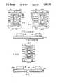
- FIG. 1is a top plan view of a typical prior art leadframe strip or a plurality of leadframe assemblies used for production of integrated circuits in plastic packages;
- FIG. 2is a cross sectional view of a single leadframe of FIG. 1, taken alone the lines 2--2 thereof, and showing in phantom two semiconductor chips p aced thereon;
- FIG. 3is a top plan view of a partially completed leadframe assembly according to the present invention.
- FIG. 4is a simplified cross-sectional view of the partially complete leadframe assembly of FIG. 3, taken alone the lines 4--4 thereof;
- FIG. 5is a bottom plan view of a completed leadframe assembly according to the present invention.
- FIG. 6is a top plan view of a completed leadframe assembly according to the present invention, with two chips mounted thereon;
- FIG. 7is a simplified cross sectional view of the assembly of FIG. 6, taken alone the lines 7--7 thereof;
- FIG. 8is an expanded layout of the apparatus of FIG. 6, showing the internal electrical connections established between the two chips o the leadframe assembly;
- FIG. 9is a top plan view of a leadframe assembly with four die attach paddles according to the present invention.
- FIG. 1shows a typical prior art leadframe strip 10, which is stamped from sheet metal.
- the leadframe strip 10comprises a pair of side rails 12 and 14, each having sprocket holes, such as 16 and 18, at regularly spaced intervals.
- the sprocket holescooperate during the chip assembly process with sprocket teeth in a mechanism for moving the leadframe strip through appropriate processing equipment.
- a leadframe stripgenerally has a large number of leadframe assemblies, such as the two assemblies 20 and 22, suspended between the side rails at regular intervals.
- each leadframe assemblycomprises a die attach paddle 24 supported from the side rails 12 and 14 by thin metal bridges 26 and 28, respectively.
- a plurality of connection pins or leads 30A, 30B . . . 30nare also suspended between the side rails via bridges 31 and are arrayed around the die attach paddle. These connection pins are later bonded to small wires which connect them to bonding pads, or terminals, on the semiconductor chip(s). Later in the assembly process, the bridges 26, 28 and 31 are severed, detaching the side rails 12 and 14 from the connection pin strips and electrically isolating each of the connection pins and the die attach paddle.
- the first step in creating the assembly of the present inventionis to provide a modified leadframe assembly, wherein the attach paddle is formed as or cut into two (or more) separate die attach paddles, as indicated, for example, by the paddles 24A and 24B of FIG. 3.
- a single die attach paddle 24may be cut into two or more constituent and electrically isolated die attach paddles, or die attach paddles 24A and 24B can be manufactured separately from the beginning.
- Separate die attach paddles 24A and 24Bcan be the same size or different sizes. For purposes of generality, they are indicated in the drawings to be of different sizes. The resulting arrangement appears in a simplified cross sectional view in FIG.
- a strip of polyimide tapeis applied, using a non conductive adhesive such as a silicone adhesive, to the reverse sides of the paddles 24A and 24B (i.e., the side which does not receive the chips).
- a non conductive adhesivesuch as a silicone adhesive
- a suitable materialis Kapton® tape manufactured by E. I. duPont de Nemours of Wilmington, Del.
- the two chipsare glued to the top surfaces of the respective die attach paddles 24A and 24B, as shown in FIG. 6.
- the resulting arrangementis shown in the simplified cross-section of FIG. 7.
- the two chips 40 and 42are wired to the connection pins, as shown in FIG. 8 by, for example, the wires 60A and 60B. They are also wired to each other by connecting appropriate conductors indicated generally at 62, between opposing bonding pads on the two chips. Lastly, the entire assembly is encapsulated in a plastic package.
- the polyimide tapemay be obtained with an already applied coating of a pressure sensitive adhesive, so that it can simply be pressed in place.
- the polyimide tapemay be secured to the die attach paddles with a heat activated adhesive.
- a prime benefit of this inventionis its low cost.
- a total of 1-2 ⁇is added over the cost of the standard leadframe of the type shown in Fiq. 1.
- the use of a ceramic substrateadds about 15-25 ⁇ to fabrication costs, and the use of a resin substrate adds about 15 to fabrication cost.
- Up to four (or more) chipsmay be placed in a single package using this approach, using (for example) the arrangement shown in FIG. 9, where four separate die attach paddles 70A, 70B, 70C and 70D each have one bridge or tie bar (72A, 72B, 72C and 72D, respectively) connecting them to the side rail of the leadframe strip.
- a single strip of dielectric tape 74may be applied across the backs of all the attach paddles. This can permit extremely complex functionality to be provided in a single package at low cost.
Landscapes
- Physics & Mathematics (AREA)
- Condensed Matter Physics & Semiconductors (AREA)
- General Physics & Mathematics (AREA)
- Engineering & Computer Science (AREA)
- Computer Hardware Design (AREA)
- Microelectronics & Electronic Packaging (AREA)
- Power Engineering (AREA)
- Lead Frames For Integrated Circuits (AREA)
Abstract
Description
Claims (5)
Priority Applications (1)
| Application Number | Priority Date | Filing Date | Title |
|---|---|---|---|
| US07/300,328US5084753A (en) | 1989-01-23 | 1989-01-23 | Packaging for multiple chips on a single leadframe |
Applications Claiming Priority (1)
| Application Number | Priority Date | Filing Date | Title |
|---|---|---|---|
| US07/300,328US5084753A (en) | 1989-01-23 | 1989-01-23 | Packaging for multiple chips on a single leadframe |
Publications (1)
| Publication Number | Publication Date |
|---|---|
| US5084753Atrue US5084753A (en) | 1992-01-28 |
Family
ID=23158650
Family Applications (1)
| Application Number | Title | Priority Date | Filing Date |
|---|---|---|---|
| US07/300,328Expired - LifetimeUS5084753A (en) | 1989-01-23 | 1989-01-23 | Packaging for multiple chips on a single leadframe |
Country Status (1)
| Country | Link |
|---|---|
| US (1) | US5084753A (en) |
Cited By (29)
| Publication number | Priority date | Publication date | Assignee | Title |
|---|---|---|---|---|
| US5245215A (en)* | 1982-01-11 | 1993-09-14 | Kabushiki Kaisha Toshiba | Multichip packaged semiconductor device and method for manufacturing the same |
| US5420459A (en)* | 1992-12-22 | 1995-05-30 | Kabushiki Kaisha Toshiba | Resin encapsulation type semiconductor device having an improved lead configuration |
| US5598038A (en)* | 1993-11-11 | 1997-01-28 | Nec Corporation | Resin encapsulated semiconductor device |
| US5640044A (en)* | 1994-04-15 | 1997-06-17 | Matsushita Electric Industrial Co., Ltd. | Semiconductor device and method of producing said semiconductor device |
| DE19714470A1 (en)* | 1996-06-07 | 1997-12-11 | Hewlett Packard Co | Multichip interconnection for multichip module containing programmable logic component |
| US5710064A (en)* | 1994-08-16 | 1998-01-20 | Samsung Electronics Co., Ltd. | Method for manufacturing a semiconductor package |
| US5789816A (en)* | 1996-10-04 | 1998-08-04 | United Microelectronics Corporation | Multiple-chip integrated circuit package including a dummy chip |
| US5814884A (en)* | 1996-10-24 | 1998-09-29 | International Rectifier Corporation | Commonly housed diverse semiconductor die |
| WO1999045591A1 (en)* | 1998-03-06 | 1999-09-10 | Microchip Technology Incorporated | An integrated circuit package having interchip bonding and method therefor |
| US6144093A (en)* | 1998-04-27 | 2000-11-07 | International Rectifier Corp. | Commonly housed diverse semiconductor die with reduced inductance |
| DE19957089A1 (en)* | 1999-11-29 | 2001-06-07 | Possehl Electronic Gmbh | Chip carrier or lead-frame with carrier plate comprising at least two spatially- and electrically-isolated part-pieces, has part-pieces of carrier plate retained by frame-parts made of electrically-insulated material |
| US6396130B1 (en) | 2001-09-14 | 2002-05-28 | Amkor Technology, Inc. | Semiconductor package having multiple dies with independently biased back surfaces |
| US6424035B1 (en)* | 1998-11-05 | 2002-07-23 | Fairchild Semiconductor Corporation | Semiconductor bilateral switch |
| US6528868B1 (en)* | 1998-02-21 | 2003-03-04 | Robert Bosch Gmbh | Lead frame device and method for producing the same |
| US6593622B2 (en)* | 2001-05-02 | 2003-07-15 | International Rectifier Corporation | Power mosfet with integrated drivers in a common package |
| US6723620B1 (en)* | 1999-11-24 | 2004-04-20 | International Rectifier Corporation | Power semiconductor die attach process using conductive adhesive film |
| US20050006731A1 (en)* | 2003-07-10 | 2005-01-13 | General Semiconductor, Inc. | Surface mount multichip devices |
| US20070045809A1 (en)* | 2005-09-01 | 2007-03-01 | Wheless Thomas O Jr | Quad flat pack (QFP) package and flexible power distribution method therefor |
| WO2007102042A1 (en)* | 2006-03-09 | 2007-09-13 | Infineon Technologies Ag | A multi-chip electronic package with reduced stress |
| US20080012116A1 (en)* | 2006-07-13 | 2008-01-17 | Samsung Electronics Co., Ltd. | Semiconductor device and method of forming the same |
| US20090085181A1 (en)* | 2007-09-28 | 2009-04-02 | Advincula Jr Abelardo Hadap | Integrated circuit package system with multiple die |
| US20100001384A1 (en)* | 2008-07-01 | 2010-01-07 | Henry Descalzo Bathan | Integrated circuit package system with lead-frame paddle scheme for single axis partial saw isolation |
| US20100032816A1 (en)* | 2008-08-05 | 2010-02-11 | Infineon Technologies Ag | Electronic Device and Method of Manufacturing Same |
| US20100123255A1 (en)* | 2007-02-16 | 2010-05-20 | Richtek Technology Corp. | Electronic package structure and method |
| US20130105957A1 (en)* | 2011-10-31 | 2013-05-02 | Sony Corporation | Lead frame semiconductor device |
| US8936971B2 (en) | 2010-09-16 | 2015-01-20 | Stats Chippac Ltd. | Integrated circuit packaging system with die paddles and method of manufacture thereof |
| US8951847B2 (en) | 2012-01-18 | 2015-02-10 | Intersil Americas LLC | Package leadframe for dual side assembly |
| CN105470245A (en)* | 2014-09-30 | 2016-04-06 | 瑞萨电子株式会社 | Semiconductor device |
| EP3787019A4 (en)* | 2018-04-25 | 2021-05-05 | Mitsubishi Electric Corporation | COMMON BASE PLATE AND ASSEMBLED SEMI-CONDUCTOR MODULE |
Citations (22)
| Publication number | Priority date | Publication date | Assignee | Title |
|---|---|---|---|---|
| US3938177A (en)* | 1973-06-25 | 1976-02-10 | Amp Incorporated | Narrow lead contact for automatic face down bonding of electronic chips |
| US3978516A (en)* | 1974-01-02 | 1976-08-31 | Texas Instruments Incorporated | Lead frame assembly for a packaged semiconductor microcircuit |
| US4089733A (en)* | 1975-09-12 | 1978-05-16 | Amp Incorporated | Method of forming complex shaped metal-plastic composite lead frames for IC packaging |
| JPS54161270A (en)* | 1978-06-09 | 1979-12-20 | Nec Corp | Lead frame for integrated-circuit device |
| US4203792A (en)* | 1977-11-17 | 1980-05-20 | Bell Telephone Laboratories, Incorporated | Method for the fabrication of devices including polymeric materials |
| US4264917A (en)* | 1978-10-19 | 1981-04-28 | Compagnie Internationale Pour L'informatique Cii-Honeywell Bull | Flat package for integrated circuit devices |
| US4282544A (en)* | 1977-12-12 | 1981-08-04 | Motorola Inc. | Encapsulated hybrid circuit assembly |
| JPS5766655A (en)* | 1980-10-09 | 1982-04-22 | Mitsubishi Electric Corp | Lead frame for semiconductor device |
| US4331831A (en)* | 1980-11-28 | 1982-05-25 | Bell Telephone Laboratories, Incorporated | Package for semiconductor integrated circuits |
| JPS58178544A (en)* | 1982-04-12 | 1983-10-19 | Matsushita Electronics Corp | Lead frame |
| JPS58191457A (en)* | 1982-05-04 | 1983-11-08 | Toshiba Corp | semiconductor equipment |
| US4450461A (en)* | 1981-07-24 | 1984-05-22 | General Electric Company | Low cost high isolation voltage optocoupler with improved light transmissivity |
| JPS607159A (en)* | 1983-06-24 | 1985-01-14 | Toshiba Corp | Resin-encapsulated semiconductor device and its manufacturing method |
| WO1985001835A1 (en)* | 1983-10-21 | 1985-04-25 | American Telephone & Telegraph Company | Semiconductor integrated circuit including a lead frame chip support |
| US4532538A (en)* | 1981-02-20 | 1985-07-30 | Siemens Aktiengesellschaft | Semiconductor arrangement with connector conductors cut out of sheetmetal |
| JPS6235655A (en)* | 1985-08-09 | 1987-02-16 | Hitachi Ltd | Semiconductor integrated circuit device |
| JPS62274645A (en)* | 1986-05-23 | 1987-11-28 | Hitachi Ltd | Lead frame and electronic device using it |
| JPS6356950A (en)* | 1986-08-28 | 1988-03-11 | Fuji Electric Co Ltd | Composite integrated circuit device |
| GB2196475A (en)* | 1986-09-23 | 1988-04-27 | Royal Ordnance Plc | Timer package |
| US4794431A (en)* | 1986-04-21 | 1988-12-27 | International Rectifier Corporation | Package for photoactivated semiconductor device |
| JPS6476741A (en)* | 1987-09-17 | 1989-03-22 | Hitachi Ltd | Semiconductor device |
| US4878106A (en)* | 1986-12-02 | 1989-10-31 | Anton Piller Gmbh & Co. Kg | Semiconductor circuit packages for use in high power applications and method of making the same |
- 1989
- 1989-01-23USUS07/300,328patent/US5084753A/ennot_activeExpired - Lifetime
Patent Citations (22)
| Publication number | Priority date | Publication date | Assignee | Title |
|---|---|---|---|---|
| US3938177A (en)* | 1973-06-25 | 1976-02-10 | Amp Incorporated | Narrow lead contact for automatic face down bonding of electronic chips |
| US3978516A (en)* | 1974-01-02 | 1976-08-31 | Texas Instruments Incorporated | Lead frame assembly for a packaged semiconductor microcircuit |
| US4089733A (en)* | 1975-09-12 | 1978-05-16 | Amp Incorporated | Method of forming complex shaped metal-plastic composite lead frames for IC packaging |
| US4203792A (en)* | 1977-11-17 | 1980-05-20 | Bell Telephone Laboratories, Incorporated | Method for the fabrication of devices including polymeric materials |
| US4282544A (en)* | 1977-12-12 | 1981-08-04 | Motorola Inc. | Encapsulated hybrid circuit assembly |
| JPS54161270A (en)* | 1978-06-09 | 1979-12-20 | Nec Corp | Lead frame for integrated-circuit device |
| US4264917A (en)* | 1978-10-19 | 1981-04-28 | Compagnie Internationale Pour L'informatique Cii-Honeywell Bull | Flat package for integrated circuit devices |
| JPS5766655A (en)* | 1980-10-09 | 1982-04-22 | Mitsubishi Electric Corp | Lead frame for semiconductor device |
| US4331831A (en)* | 1980-11-28 | 1982-05-25 | Bell Telephone Laboratories, Incorporated | Package for semiconductor integrated circuits |
| US4532538A (en)* | 1981-02-20 | 1985-07-30 | Siemens Aktiengesellschaft | Semiconductor arrangement with connector conductors cut out of sheetmetal |
| US4450461A (en)* | 1981-07-24 | 1984-05-22 | General Electric Company | Low cost high isolation voltage optocoupler with improved light transmissivity |
| JPS58178544A (en)* | 1982-04-12 | 1983-10-19 | Matsushita Electronics Corp | Lead frame |
| JPS58191457A (en)* | 1982-05-04 | 1983-11-08 | Toshiba Corp | semiconductor equipment |
| JPS607159A (en)* | 1983-06-24 | 1985-01-14 | Toshiba Corp | Resin-encapsulated semiconductor device and its manufacturing method |
| WO1985001835A1 (en)* | 1983-10-21 | 1985-04-25 | American Telephone & Telegraph Company | Semiconductor integrated circuit including a lead frame chip support |
| JPS6235655A (en)* | 1985-08-09 | 1987-02-16 | Hitachi Ltd | Semiconductor integrated circuit device |
| US4794431A (en)* | 1986-04-21 | 1988-12-27 | International Rectifier Corporation | Package for photoactivated semiconductor device |
| JPS62274645A (en)* | 1986-05-23 | 1987-11-28 | Hitachi Ltd | Lead frame and electronic device using it |
| JPS6356950A (en)* | 1986-08-28 | 1988-03-11 | Fuji Electric Co Ltd | Composite integrated circuit device |
| GB2196475A (en)* | 1986-09-23 | 1988-04-27 | Royal Ordnance Plc | Timer package |
| US4878106A (en)* | 1986-12-02 | 1989-10-31 | Anton Piller Gmbh & Co. Kg | Semiconductor circuit packages for use in high power applications and method of making the same |
| JPS6476741A (en)* | 1987-09-17 | 1989-03-22 | Hitachi Ltd | Semiconductor device |
Cited By (55)
| Publication number | Priority date | Publication date | Assignee | Title |
|---|---|---|---|---|
| US5245215A (en)* | 1982-01-11 | 1993-09-14 | Kabushiki Kaisha Toshiba | Multichip packaged semiconductor device and method for manufacturing the same |
| US5352632A (en)* | 1991-02-08 | 1994-10-04 | Kabushiki Kaisha Toshiba | Multichip packaged semiconductor device and method for manufacturing the same |
| US5420459A (en)* | 1992-12-22 | 1995-05-30 | Kabushiki Kaisha Toshiba | Resin encapsulation type semiconductor device having an improved lead configuration |
| US5598038A (en)* | 1993-11-11 | 1997-01-28 | Nec Corporation | Resin encapsulated semiconductor device |
| US5640044A (en)* | 1994-04-15 | 1997-06-17 | Matsushita Electric Industrial Co., Ltd. | Semiconductor device and method of producing said semiconductor device |
| US5783463A (en)* | 1994-04-15 | 1998-07-21 | Matsushita Electric Industrial Co., Ltd. | Semiconductor device and method of producing said semiconductor device |
| US5710064A (en)* | 1994-08-16 | 1998-01-20 | Samsung Electronics Co., Ltd. | Method for manufacturing a semiconductor package |
| DE19714470A1 (en)* | 1996-06-07 | 1997-12-11 | Hewlett Packard Co | Multichip interconnection for multichip module containing programmable logic component |
| US5723906A (en)* | 1996-06-07 | 1998-03-03 | Hewlett-Packard Company | High-density wirebond chip interconnect for multi-chip modules |
| US5789816A (en)* | 1996-10-04 | 1998-08-04 | United Microelectronics Corporation | Multiple-chip integrated circuit package including a dummy chip |
| US6133632A (en)* | 1996-10-24 | 2000-10-17 | International Rectifier Corp. | Commonly housed diverse semiconductor die |
| US6297552B1 (en) | 1996-10-24 | 2001-10-02 | International Rectifier Corp. | Commonly housed diverse semiconductor die |
| US5814884A (en)* | 1996-10-24 | 1998-09-29 | International Rectifier Corporation | Commonly housed diverse semiconductor die |
| US6404050B2 (en) | 1996-10-24 | 2002-06-11 | International Rectifier Corporation | Commonly housed diverse semiconductor |
| US6528868B1 (en)* | 1998-02-21 | 2003-03-04 | Robert Bosch Gmbh | Lead frame device and method for producing the same |
| US6333549B2 (en) | 1998-03-06 | 2001-12-25 | Microchip Technology Incorporated | Integrated circuit package having interchip bonding and method therefor |
| WO1999045591A1 (en)* | 1998-03-06 | 1999-09-10 | Microchip Technology Incorporated | An integrated circuit package having interchip bonding and method therefor |
| US6159765A (en)* | 1998-03-06 | 2000-12-12 | Microchip Technology, Incorporated | Integrated circuit package having interchip bonding and method therefor |
| US6144093A (en)* | 1998-04-27 | 2000-11-07 | International Rectifier Corp. | Commonly housed diverse semiconductor die with reduced inductance |
| US6424035B1 (en)* | 1998-11-05 | 2002-07-23 | Fairchild Semiconductor Corporation | Semiconductor bilateral switch |
| US6723620B1 (en)* | 1999-11-24 | 2004-04-20 | International Rectifier Corporation | Power semiconductor die attach process using conductive adhesive film |
| DE19957089A1 (en)* | 1999-11-29 | 2001-06-07 | Possehl Electronic Gmbh | Chip carrier or lead-frame with carrier plate comprising at least two spatially- and electrically-isolated part-pieces, has part-pieces of carrier plate retained by frame-parts made of electrically-insulated material |
| DE19957089C2 (en)* | 1999-11-29 | 2003-01-30 | Possehl Electronic Gmbh | System carrier with a carrier plate for electronic components and method for its production |
| US6593622B2 (en)* | 2001-05-02 | 2003-07-15 | International Rectifier Corporation | Power mosfet with integrated drivers in a common package |
| USRE41719E1 (en)* | 2001-05-02 | 2010-09-21 | International Rectifier Corporation | Power MOSFET with integrated drivers in a common package |
| US6396130B1 (en) | 2001-09-14 | 2002-05-28 | Amkor Technology, Inc. | Semiconductor package having multiple dies with independently biased back surfaces |
| US6919625B2 (en) | 2003-07-10 | 2005-07-19 | General Semiconductor, Inc. | Surface mount multichip devices |
| US20050248007A1 (en)* | 2003-07-10 | 2005-11-10 | O'shea Paddy | Surface mount multichip devices |
| US7242078B2 (en) | 2003-07-10 | 2007-07-10 | General Semiconductor, Inc. | Surface mount multichip devices |
| US7525183B2 (en) | 2003-07-10 | 2009-04-28 | General Semiconductor, Inc. | Surface mount multichip devices |
| US20080017959A1 (en)* | 2003-07-10 | 2008-01-24 | O'shea Paddy | Surface mount multichip devices |
| US20050006731A1 (en)* | 2003-07-10 | 2005-01-13 | General Semiconductor, Inc. | Surface mount multichip devices |
| US20070045809A1 (en)* | 2005-09-01 | 2007-03-01 | Wheless Thomas O Jr | Quad flat pack (QFP) package and flexible power distribution method therefor |
| US7800205B2 (en)* | 2005-09-01 | 2010-09-21 | Avago Technologies General Ip (Singapore) Pte. Ltd. | Quad flat pack (QFP) package and flexible power distribution method therefor |
| US20090008756A1 (en)* | 2006-03-09 | 2009-01-08 | Infineon Technologies Ag | Multi-Chip Electronic Package with Reduced Stress |
| US8604595B2 (en) | 2006-03-09 | 2013-12-10 | Infineon Technologies Ag | Multi-chip electronic package with reduced stress |
| WO2007102042A1 (en)* | 2006-03-09 | 2007-09-13 | Infineon Technologies Ag | A multi-chip electronic package with reduced stress |
| US20080012116A1 (en)* | 2006-07-13 | 2008-01-17 | Samsung Electronics Co., Ltd. | Semiconductor device and method of forming the same |
| US7696615B2 (en)* | 2006-07-13 | 2010-04-13 | Samsung Electronics Co., Ltd. | Semiconductor device having pillar-shaped terminal |
| US8097952B2 (en)* | 2007-02-16 | 2012-01-17 | Richtek Technology Corp. | Electronic package structure having conductive strip and method |
| US20100123255A1 (en)* | 2007-02-16 | 2010-05-20 | Richtek Technology Corp. | Electronic package structure and method |
| US20090085181A1 (en)* | 2007-09-28 | 2009-04-02 | Advincula Jr Abelardo Hadap | Integrated circuit package system with multiple die |
| US8067825B2 (en)* | 2007-09-28 | 2011-11-29 | Stats Chippac Ltd. | Integrated circuit package system with multiple die |
| US8569872B2 (en) | 2008-07-01 | 2013-10-29 | Stats Chippac Ltd. | Integrated circuit package system with lead-frame paddle scheme for single axis partial saw isolation |
| US20100001384A1 (en)* | 2008-07-01 | 2010-01-07 | Henry Descalzo Bathan | Integrated circuit package system with lead-frame paddle scheme for single axis partial saw isolation |
| US7847375B2 (en) | 2008-08-05 | 2010-12-07 | Infineon Technologies Ag | Electronic device and method of manufacturing same |
| US20100032816A1 (en)* | 2008-08-05 | 2010-02-11 | Infineon Technologies Ag | Electronic Device and Method of Manufacturing Same |
| US8936971B2 (en) | 2010-09-16 | 2015-01-20 | Stats Chippac Ltd. | Integrated circuit packaging system with die paddles and method of manufacture thereof |
| US8928136B2 (en)* | 2011-10-31 | 2015-01-06 | Sony Corporation | Lead frame semiconductor device |
| US20130105957A1 (en)* | 2011-10-31 | 2013-05-02 | Sony Corporation | Lead frame semiconductor device |
| CN103094238B (en)* | 2011-10-31 | 2017-07-14 | 索尼公司 | Lead frame and semiconductor devices |
| US8951847B2 (en) | 2012-01-18 | 2015-02-10 | Intersil Americas LLC | Package leadframe for dual side assembly |
| CN105470245A (en)* | 2014-09-30 | 2016-04-06 | 瑞萨电子株式会社 | Semiconductor device |
| CN105470245B (en)* | 2014-09-30 | 2019-10-18 | 瑞萨电子株式会社 | Semiconductor device |
| EP3787019A4 (en)* | 2018-04-25 | 2021-05-05 | Mitsubishi Electric Corporation | COMMON BASE PLATE AND ASSEMBLED SEMI-CONDUCTOR MODULE |
Similar Documents
| Publication | Publication Date | Title |
|---|---|---|
| US5084753A (en) | Packaging for multiple chips on a single leadframe | |
| US5637828A (en) | High density semiconductor package | |
| US5563443A (en) | Packaged semiconductor device utilizing leadframe attached on a semiconductor chip | |
| US6458625B2 (en) | Multi chip semiconductor package and method of construction | |
| CA1252912A (en) | Semiconductor package with high density i/o lead connection | |
| US5373188A (en) | Packaged semiconductor device including multiple semiconductor chips and cross-over lead | |
| US6552416B1 (en) | Multiple die lead frame package with enhanced die-to-die interconnect routing using internal lead trace wiring | |
| US5620928A (en) | Ultra thin ball grid array using a flex tape or printed wiring board substrate and method | |
| US4701781A (en) | Pre-testable semiconductor die package | |
| KR100263723B1 (en) | Flexible film semiconductor package | |
| KR100226737B1 (en) | Semiconductor device stacked package | |
| US5648679A (en) | Tape ball lead integrated circuit package | |
| CA1201820A (en) | Semiconductor integrated circuit including a lead frame chip support | |
| KR100269281B1 (en) | Semiconductor device | |
| US20080182365A1 (en) | Die package with asymmetric leadframe connection | |
| KR19980042617A (en) | Wafer Level Packaging | |
| US6407333B1 (en) | Wafer level packaging | |
| US6791166B1 (en) | Stackable lead frame package using exposed internal lead traces | |
| US6774479B2 (en) | Electronic device having a semiconductor chip on a semiconductor chip connection plate and a method for producing the electronic device | |
| EP1636840B1 (en) | Micro lead frame substrate and method for its manufacture | |
| GB2174538A (en) | Semiconductor package | |
| US5719748A (en) | Semiconductor package with a bridge for chip area connection | |
| JP3466354B2 (en) | Semiconductor device | |
| KR970002136B1 (en) | Semiconductor package | |
| JPH02229461A (en) | Semiconductor device |
Legal Events
| Date | Code | Title | Description |
|---|---|---|---|
| AS | Assignment | Owner name:ANALOG DEVICES, INC., A MA CORP., MASSACHUSETTS Free format text:ASSIGNMENT OF ASSIGNORS INTEREST.;ASSIGNORS:ROBERTS, CARL M. JR.;GOIDA, THOMAS M.;REEL/FRAME:005037/0251 Effective date:19890120 | |
| FEPP | Fee payment procedure | Free format text:PAYOR NUMBER ASSIGNED (ORIGINAL EVENT CODE: ASPN); ENTITY STATUS OF PATENT OWNER: LARGE ENTITY | |
| STCF | Information on status: patent grant | Free format text:PATENTED CASE | |
| CC | Certificate of correction | ||
| FPAY | Fee payment | Year of fee payment:4 | |
| FPAY | Fee payment | Year of fee payment:8 | |
| FEPP | Fee payment procedure | Free format text:PAYER NUMBER DE-ASSIGNED (ORIGINAL EVENT CODE: RMPN); ENTITY STATUS OF PATENT OWNER: LARGE ENTITY Free format text:PAYOR NUMBER ASSIGNED (ORIGINAL EVENT CODE: ASPN); ENTITY STATUS OF PATENT OWNER: LARGE ENTITY | |
| FEPP | Fee payment procedure | Free format text:PAYER NUMBER DE-ASSIGNED (ORIGINAL EVENT CODE: RMPN); ENTITY STATUS OF PATENT OWNER: LARGE ENTITY Free format text:PAYOR NUMBER ASSIGNED (ORIGINAL EVENT CODE: ASPN); ENTITY STATUS OF PATENT OWNER: LARGE ENTITY | |
| FEPP | Fee payment procedure | Free format text:PAYER NUMBER DE-ASSIGNED (ORIGINAL EVENT CODE: RMPN); ENTITY STATUS OF PATENT OWNER: LARGE ENTITY Free format text:PAYOR NUMBER ASSIGNED (ORIGINAL EVENT CODE: ASPN); ENTITY STATUS OF PATENT OWNER: LARGE ENTITY | |
| FPAY | Fee payment | Year of fee payment:12 |