US5079426A - Multi-element-amorphous-silicon-detector-array for real-time imaging and dosimetry of megavoltage photons and diagnostic X rays - Google Patents
Multi-element-amorphous-silicon-detector-array for real-time imaging and dosimetry of megavoltage photons and diagnostic X raysDownload PDFInfo
- Publication number
- US5079426A US5079426AUS07/681,650US68165091AUS5079426AUS 5079426 AUS5079426 AUS 5079426AUS 68165091 AUS68165091 AUS 68165091AUS 5079426 AUS5079426 AUS 5079426A
- Authority
- US
- United States
- Prior art keywords
- layer
- sensor
- sensors
- contact region
- real
- Prior art date
- Legal status (The legal status is an assumption and is not a legal conclusion. Google has not performed a legal analysis and makes no representation as to the accuracy of the status listed.)
- Expired - Lifetime
Links
Images

Classifications
- A—HUMAN NECESSITIES
- A61—MEDICAL OR VETERINARY SCIENCE; HYGIENE
- A61B—DIAGNOSIS; SURGERY; IDENTIFICATION
- A61B6/00—Apparatus or devices for radiation diagnosis; Apparatus or devices for radiation diagnosis combined with radiation therapy equipment
- A61B6/02—Arrangements for diagnosis sequentially in different planes; Stereoscopic radiation diagnosis
- A61B6/03—Computed tomography [CT]
- A61B6/032—Transmission computed tomography [CT]
- A—HUMAN NECESSITIES
- A61—MEDICAL OR VETERINARY SCIENCE; HYGIENE
- A61N—ELECTROTHERAPY; MAGNETOTHERAPY; RADIATION THERAPY; ULTRASOUND THERAPY
- A61N5/00—Radiation therapy
- A61N5/10—X-ray therapy; Gamma-ray therapy; Particle-irradiation therapy
- A61N5/1048—Monitoring, verifying, controlling systems and methods
- G—PHYSICS
- G01—MEASURING; TESTING
- G01T—MEASUREMENT OF NUCLEAR OR X-RADIATION
- G01T1/00—Measuring X-radiation, gamma radiation, corpuscular radiation, or cosmic radiation
- G01T1/16—Measuring radiation intensity
- G01T1/20—Measuring radiation intensity with scintillation detectors
- G01T1/2018—Scintillation-photodiode combinations
- G01T1/20181—Stacked detectors, e.g. for measuring energy and positional information
- G—PHYSICS
- G01—MEASURING; TESTING
- G01T—MEASUREMENT OF NUCLEAR OR X-RADIATION
- G01T1/00—Measuring X-radiation, gamma radiation, corpuscular radiation, or cosmic radiation
- G01T1/16—Measuring radiation intensity
- G01T1/20—Measuring radiation intensity with scintillation detectors
- G01T1/2018—Scintillation-photodiode combinations
- G01T1/20184—Detector read-out circuitry, e.g. for clearing of traps, compensating for traps or compensating for direct hits
- G—PHYSICS
- G01—MEASURING; TESTING
- G01T—MEASUREMENT OF NUCLEAR OR X-RADIATION
- G01T1/00—Measuring X-radiation, gamma radiation, corpuscular radiation, or cosmic radiation
- G01T1/29—Measurement performed on radiation beams, e.g. position or section of the beam; Measurement of spatial distribution of radiation
- G01T1/2914—Measurement of spatial distribution of radiation
- G01T1/2921—Static instruments for imaging the distribution of radioactivity in one or two dimensions; Radio-isotope cameras
- G01T1/2928—Static instruments for imaging the distribution of radioactivity in one or two dimensions; Radio-isotope cameras using solid state detectors
- H—ELECTRICITY
- H10—SEMICONDUCTOR DEVICES; ELECTRIC SOLID-STATE DEVICES NOT OTHERWISE PROVIDED FOR
- H10F—INORGANIC SEMICONDUCTOR DEVICES SENSITIVE TO INFRARED RADIATION, LIGHT, ELECTROMAGNETIC RADIATION OF SHORTER WAVELENGTH OR CORPUSCULAR RADIATION
- H10F39/00—Integrated devices, or assemblies of multiple devices, comprising at least one element covered by group H10F30/00, e.g. radiation detectors comprising photodiode arrays
- H10F39/10—Integrated devices
- H10F39/12—Image sensors
- H10F39/18—Complementary metal-oxide-semiconductor [CMOS] image sensors; Photodiode array image sensors
- H10F39/189—X-ray, gamma-ray or corpuscular radiation imagers
- H10F39/1898—Indirect radiation image sensors, e.g. using luminescent members
- H—ELECTRICITY
- H10—SEMICONDUCTOR DEVICES; ELECTRIC SOLID-STATE DEVICES NOT OTHERWISE PROVIDED FOR
- H10F—INORGANIC SEMICONDUCTOR DEVICES SENSITIVE TO INFRARED RADIATION, LIGHT, ELECTROMAGNETIC RADIATION OF SHORTER WAVELENGTH OR CORPUSCULAR RADIATION
- H10F39/00—Integrated devices, or assemblies of multiple devices, comprising at least one element covered by group H10F30/00, e.g. radiation detectors comprising photodiode arrays
- H10F39/80—Constructional details of image sensors
- H10F39/803—Pixels having integrated switching, control, storage or amplification elements
- H—ELECTRICITY
- H10—SEMICONDUCTOR DEVICES; ELECTRIC SOLID-STATE DEVICES NOT OTHERWISE PROVIDED FOR
- H10F—INORGANIC SEMICONDUCTOR DEVICES SENSITIVE TO INFRARED RADIATION, LIGHT, ELECTROMAGNETIC RADIATION OF SHORTER WAVELENGTH OR CORPUSCULAR RADIATION
- H10F39/00—Integrated devices, or assemblies of multiple devices, comprising at least one element covered by group H10F30/00, e.g. radiation detectors comprising photodiode arrays
- H10F39/80—Constructional details of image sensors
- H10F39/804—Containers or encapsulations
- A—HUMAN NECESSITIES
- A61—MEDICAL OR VETERINARY SCIENCE; HYGIENE
- A61N—ELECTROTHERAPY; MAGNETOTHERAPY; RADIATION THERAPY; ULTRASOUND THERAPY
- A61N5/00—Radiation therapy
- A61N5/10—X-ray therapy; Gamma-ray therapy; Particle-irradiation therapy
- A61N5/1048—Monitoring, verifying, controlling systems and methods
- A61N5/1049—Monitoring, verifying, controlling systems and methods for verifying the position of the patient with respect to the radiation beam
- A61N2005/1054—Monitoring, verifying, controlling systems and methods for verifying the position of the patient with respect to the radiation beam using a portal imaging system
- A—HUMAN NECESSITIES
- A61—MEDICAL OR VETERINARY SCIENCE; HYGIENE
- A61N—ELECTROTHERAPY; MAGNETOTHERAPY; RADIATION THERAPY; ULTRASOUND THERAPY
- A61N5/00—Radiation therapy
- A61N5/10—X-ray therapy; Gamma-ray therapy; Particle-irradiation therapy
- A61N5/1048—Monitoring, verifying, controlling systems and methods
- A61N5/1071—Monitoring, verifying, controlling systems and methods for verifying the dose delivered by the treatment plan
- A61N2005/1072—Monitoring, verifying, controlling systems and methods for verifying the dose delivered by the treatment plan taking into account movement of the target
- A—HUMAN NECESSITIES
- A61—MEDICAL OR VETERINARY SCIENCE; HYGIENE
- A61N—ELECTROTHERAPY; MAGNETOTHERAPY; RADIATION THERAPY; ULTRASOUND THERAPY
- A61N5/00—Radiation therapy
- A61N5/10—X-ray therapy; Gamma-ray therapy; Particle-irradiation therapy
- A61N5/1048—Monitoring, verifying, controlling systems and methods
- A61N5/1049—Monitoring, verifying, controlling systems and methods for verifying the position of the patient with respect to the radiation beam
- H—ELECTRICITY
- H01—ELECTRIC ELEMENTS
- H01L—SEMICONDUCTOR DEVICES NOT COVERED BY CLASS H10
- H01L2924/00—Indexing scheme for arrangements or methods for connecting or disconnecting semiconductor or solid-state bodies as covered by H01L24/00
- H01L2924/0001—Technical content checked by a classifier
- H01L2924/0002—Not covered by any one of groups H01L24/00, H01L24/00 and H01L2224/00
Definitions
- the present inventionpertains generally to the field of radiation detecting devices and, more particularly, to the field of real-time radiation imaging devices.
- the maximum dosebe delivered to the target volume and the minimum dose be delivered to the surrounding tissue.
- Prior to treatmentwhich typically consists of irradiating the patient on a daily basis for several weeks, the patient undergoes a number of preparatory steps in order to identify the region to be irradiated and to determine a "treatment plan" specifying exactly how this irradiation is to be performed. Often, one of these steps is to place the patient on a "treatment simulator", which simulates the motions and geometry of the therapy machine, and which makes diagnostic quality fluoroscopic and radiographic x-ray images.
- the fluoroscopic imagingallows a real-time means of simultaneously observing patient anatomy and manipulating the position of the patient so as to achieve a desired patient orientation with respect to the simulated treatment beam.
- current fluoroscopic devicesuse large cumbersome image-intensifier tubes which restrict the possible motions of the simulator, thereby limiting the treatment positions that can be simulated.
- a permanent record of imaging information from the simulatoris achieved by means of radiographic imaging with film as well as storage of the fluoroscopic images. These images are used to provide information which contributes to deciding what the target region should be and how the actual treatment is performed, i.e., what geometric and dosimetric combination of megavoltage beams to use to satisfactorily irradiate the target region but spare the surrounding normal tissues.
- a treatment planhas been determined, often with the assistance of a computer which allows, among other things, manipulation of the simulation information as well as CT or other imaging information, the patient is typically taken back to the simulator for a verification-simulation in order to verify the geometric correctness of the plan.
- Radiation detecting devicesare taught in Hynecek, U.S. Pat. No. 4,679,212; Luderer et al., U.S. Pat. No. 4,250,385; DiBianca, U.S. Pat. No. 4,707,608; Haque, U.S. Pat. No. 4,288,264; Kruger, U.S. Pat. No. Re. 32,164; Barnes, U.S. Pat. No. 4,626,688; and DiBianca et al., U.S. Pat. No. 4,525,628; however, these detectors do not make possible real-time imaging for megavoltage photons.
- Imaging equipmenthas been developed based on the use of photostimulable phosphors wherein an image receptor plate coated with such phosphors is exposed to a radiation beam and then "read out" by means of laser stimulated luminescence with direct conversion of the light to digital form.
- this technologyappears to offer no possibility of real-time imaging.
- Efforts to develop imagers based on camera-fluoroscopy combinationshave produced images of greatly varying quality at rates ranging from two images a second to one image every eight seconds.
- such a camera's expensive and delicate imaging electronicswould be irreversibly damaged after approximately 10-130 kilorads of dose.
- mirrorsare used to reflect the light image produced by a metal-phosphor screen combination to a camera sitting outside of the direct radiation field.
- the fibersmake up a 40 ⁇ 40 cm 2 surface, 12 cm thick, which sits in the beam behind a metal-fluorescence screen and "pipes" the light to a video camera.
- the optical fibersare bunched together in bundles of 1.5 ⁇ 1.5 cm 2 at the input end and the imager has a thickness of 12 cm.
- the optical fibershave to be bent to such an extent that light is lost due to the fact that the critical angle is exceeded.
- the systemcurrently has a light collection efficiency no greater than that of the mirror-camera system and, like those systems, is rather bulky.
- the quantum sinkis the light collection stage rather than the stage where X rays are converted to high-energy electrons which enter into the phosphor.
- the quality and speed of imaging in the above systemsare adversely affected.
- the materials for a real-time imager for megavoltage photon radiation therapycare must be taken that the materials can withstand high levels of radiation exposure over long durations of time.
- the radiation detecting elementsbe arranged over a relatively large surface area. For instance, a detection surface of at least 25 ⁇ 25 cm 2 is necessary for head and neck portals. For pelvic, abdominal and thoracic portals, a surface area of 50 ⁇ 50 cm 2 is desirable. Though solid state imagers are highly desirable, the manufacture of crystalline semiconductor detectors over such an area is certainly prohibitively expensive.
- Amorphous silicon ionizing particle detectors made of hydrogenated amorphous siliconare known which can detect the presence, position and amount of high energy ionizing particles, see Street et al, U.S. Pat. No. 4,785,186; however, the patent does not teach how a--Si:H photodiodes can be utilized in coordination with other elements to obtain a real-time imaging device.
- RougeotU.S. Pat. No. 4,799,094, teaches a photosensitive device having an array of p-doped floating grids which connect with a substrate of lightly n-doped hydrogenated amorphous silicon. Since Rougeot uses transistors as light detectors, the quantity of electron-hole pairs generated would appear quite insufficient to realize real-time imaging.
- one object of the present inventionis to achieve a pulse-by-pulse monitoring of the centroid of a transmitted megavoltage radiation beam.
- Another objectis to obtain x-ray-like images of the patient for real-time portal localization and verification imaging using megavoltage beams.
- Yet another objectis to measure the transmitted dose of the radiation field.
- a further objectis to obtain real-time diagnostic quality images with a treatment simulator with far less restrictions of motion due to the presence of the imager.
- the real-time megavoltage imaging devicehas a conversion layer for converting photons from the megavoltage radiation bursts into electrons, a scintillation layer in which the electrons created in the conversion layer create visible light photons, and an upper electrode layer which is transparent and allows the visible light from the scintillation layer to pass through.
- a plurality of a--Si:H sensorsis arranged in rows and columns to form a radiation detecting surface area. Each a--Si:H sensor is paired with a thin film field effect transistor. The RC time constant of the imaging device is calculated by multiplying the resistance of the transistor by the capacitance of the a--Si:H sensor.
- the high energy electrons and visible light photons incident upon the sensorsconstitute an imaging signal. Sufficient amounts of this imaging signal can be detected, creating electron-hole pairs which are stored in the capacitance of the sensors. Thereafter this signal can be read out on a time scale determined by the RC time constant so that real-time imaging is made possible.
- an array dedicated to determining the position of the scanning beamcould be positioned under an array dedicated to imaging the megavoltage photon beam.
- an array dedicated to real-time diagnostic x-ray imagingcould be positioned over an array dedicated to real-time megavoltage imaging. Such positioning would offer tremendous advantages to radiation therapy.
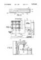
- FIG. 1is a cross-sectional side view of the present invention.
- FIG. 2is a top view illustrating the array of sensors and transistors.
- FIG. 3is a cut away perspective side view of the sensor array enclosed in a shielded housing.
- FIG. 4is a schematic block diagram illustrating interfacing of sensors and transistors with known support electronics.
- FIG. 5is a general illustration showing how the present invention is utilized in a clinical setting.
- a sensor 30 and thin-film field effect transistor 52are shown mounted upon a glass substrate 12.
- the gate contact region 14 of the thin-film field effect transistoris seen to be positioned atop the glass substrate 12.
- a gate dielectric layer 16 of silicon nitride Si 3 N 4which also makes contact with the glass substrate 12.
- a--Si:H layer 18is an a--Si:H layer 18.
- a second gate dielectric layer 24made of silicon nitride. Adjacent to the sides of the lower portion of the second gate dielectric layer 24 are located n+ doped channel layers 25, 29 which are positioned so as to sandwich the lower portions of the second gate dielectric layer 24 therebetween. A drain contact region 26 and a source contact region 28 are positioned so as to sandwich the upper portion of the second gate dielectric layer 24 between them.
- These structured layers above and to the side of the gate contact regionconstitute a thin-film field effect transistor 52.
- microcrystalline silicon thin-film-transistorscan be implemented to achieve faster read-out-speed.
- This thin-film field effect transistor 52is connected to a sensor 30 which constitutes a p-i-n photodiode.
- the sensor 30is connected to the source contact region 28 of the thin-film field effect transistor 52 by means of lower electrode layer 22.
- a--Si:H layer 36Above lower electrode layer 22 is p+ doped a--Si:H layer 36, layer 36 being approximately 400 ⁇ thick. Above layer 36 is an intrinsic a--Si:H layer 34 which is at least one micron thick and preferably being approximately 3 microns or more thick for reasons which will be subsequently discussed. Above the intrinsic layer 34 is an n+ doped layer of a--Si:H 32, which is approximately 100 ⁇ thick.
- n+ doped layer 32lies the upper electrode 38 which is made of a material transparent to visible light.
- a materialsuch as indium tin oxide (ITO) is a suitable material for the upper electrode 38.
- a scintillating layer 44 for purposes of converting electrons to visible lightis located directly above and preferably makes contact with the transparent upper electrode 38.
- Scintillating layer 44may be a CRONEXTM scintillating screen made by Dupont, a LANEXTM scintillating screen made by Kodak or other suitable material.
- a photon-to-electron conversion layer 46is located directly above and makes contact with scintillating layer 44.
- Conversion layer 46is a 1 millimeter thick copper sheet; however, the thickness can be varied depending on the energy level of the radiation to which it is exposed.
- a 1 mm thick copper sheet when combined with a CRONEXTM scintillating screen and exposed to a megavoltage ( ⁇ 3-50 MV) photon beamproduces pulses of light for about 10 microseconds.
- a 1 mm thick copper sheet when combined with a LANEXTM scintillating screenproduces pulses of light for about 1 millisecond when exposed to a megavoltage beam.
- a suitable phosphor materialmay be deposited directly onto the sensors or onto the photon-to-electron converter in order to optimize the spatial resolution of the imager.
- the interaction of X rays with the scintillation layer 44is such that the conversion layer 46 is not necessary.
- polyimide 42is placed over the field effect transistor 52 and between sensors 30 to provide insulation.
- FIG. 2shows an array of sensors 50 according to the present invention.
- Biasing lines 40are seen to connect the sensors 30 by being connected across the upper electrode layer 38 of each sensor in a given row.
- a metal layer(not shown), e.g. of aluminum, is coincident with those regions of biasing lines 40 which are located between the sensors 30. Such a metal layer serves to shield the transistors 52 from light.
- Signal lines 54are shown to connect to the drain of each field effect transistor 52 in a given row.
- a drain electrode layer 23extends away from a side of drain contact region 26.
- Metallization(not shown) extends vertically downward from the end 27 of the drain electrode layer 23 away from transistor 52. This metallization is constructed to connect with a signal line 54 which lies on the substrate 12 in front of the sensor 30.
- Gate select lines 56(FIG. 2) are seen to connect the gates of the thin-film field effect transistors located in a given column.
- the sensors and thin-film field effect transistorsare arranged in rows and columns so as to form an array 50 mounted upon a glass substrate 12 and form a detection panel.
- a 25.6 ⁇ 25.6 cm 2 imaging panelis made of approximately 65,536 or more individual sensors.
- a typical imaging panelwill have a 256 ⁇ 256 array of sensors or more. Each sensor is approximately 0.9 millimeters long or smaller with a density of at least 1 sensor per square millimeter being desired.
- Four panels of the 25.6 ⁇ 25.6 cm 2 sensor arrayscan be combined to form a roughly 50 ⁇ 50 cm 2 surface so that the invention can be utilized for virtually any imaging function.
- FIG. 4shows the layout of the read-out electronics.
- Each gate select line 56is addressed sequentially with a shift register.
- the signal lines 54are connected to an amplifier and switching electronics. Either a charge or voltage amplifier may be used. If it is the latter, then a capacitor is included on the array at each signal line. The charge or voltage is sensed just after the end of each gate pulse, after which the signal line is reset to ground potential before the next gate pulse.
- a radiation beam 10is directed upon the photon-to-electron conversion layer 46 which converts the photons of the radiation beam to electrons, some of whose energy is absorbed in scintillating layer 44 and thereby converted to visible light.
- This visible lightpasses through the transparent upper electrode 38 and into the sensor 30 where electron-hole pairs are generated in the intrinsic layer 34.
- the present inventionallows 70 to 95 percent of the visible light photons emitted from scintillating layer 44 to be converted to electron-hole pairs in the sensors.
- the sensor 30has a capacitive effect when a reverse bias is applied to all of the sensors by means of the biasing lines 40. This reverse bias causes the electron-hole pairs to be attracted to the upper and lower electrodes 38 and 22 where the signal generated from the radiation bursts are thus stored.
- the applied biasmust increase proportionally in order to ensure that the electron-hole pairs generated throughout the intrinsic layer are efficiently collected and positioned at the upper and lower electrodes.
- a thickness of 1 micronis sufficient to absorb all the visible light from the phosphor. The choice of thickness is determined in part by the capacitance requirements of the sensor.
- the size of the signals stored by the capacitance of the sensorsconstitutes the information from which the images are produced.
- the speed at which the size of these signals may be sampledis characterized by a time constant, RC, which is given by the product of the sensor capacitance and the on-resistance of the transistor.
- RCtime constant
- a second constraint upon the sampling period for certain applications of radiation therapyis the requirement that the array be capable of being read out after every burst of radiation. This latter constraint demands that the RC time constant be less than the time interval between radiation pulses divided by the number of columns in the array. The former considerations of noise would encourage even further reductions.
- W and Lare the width and length of the transistor
- ⁇ FE⁇ 0.5 cm 2 /Vsec
- V T1V
- C g⁇ 10 -8 F/cm 2
- W/Lis 10-100 so that R ⁇ 0.1-1 Mohm. If the sensor capacitance is 50 pF, then the RC time constant can be as small as 5 microseconds, thus satisfying the speed requirements.
- a column of sensorscan be read out approximately every 10 microseconds. Therefore to read 256 columns would take 2.56 milliseconds. If the interval between radiation bursts is set at 2.56 milliseconds, this would give sufficient time to read out 256 columns in between radiation bursts. Thus, the time interval between radiation bursts, if set at 2.56 milliseconds, when divided by 256 rows would yield a time of 10 microseconds. Since the signal decays in an exponential fashion, the majority of the signal information is obtained during one time constant. Therefore, for this example, the desired time constant for the imaging device would be less than 10 microseconds.
- each sensor and the resistance of each transistorshould be designed so that the product of their respective capacitances and resistances is equal to the time constant desired. With the signal information stored in the sensor being adequately sampled during a time scale determined by the time constant, real time imaging is made possible.
- the intrinsic layer 34must be at least 1 micron thick or greater for purposes of converting and collecting photons over virtually the entire visible spectrum. As the intrinsic layer increases in thickness, capacitance diminishes and the ionization signal from high energy quanta increases. Furthermore, as the aspect ratio (W/L) of the thin-film field effect transistor is increased, resistance is reduced. Thus, by widening the channel of the field effect transistor, an increase in the aspect ratio and consequently a decrease in resistance will be realized. Also, resistance can be reduced by increasing the bias received by the gate of the field effect transistor.
- the signal stored due to the capacitance of the sensor 30is released from the source region to the drain region of the field effect transistor and is channeled through the signal lines 54 and on to interfacing electronics.
- the ultimate limitation to the signal-to-noise ratiois the quantum noise of (i.e., statistical variations in) the number of high energy photons converting to high energy electrons which deposit energy in the phosphor, and an ideal detector will introduce no significant additional noise.
- a typical gamma-ray burstwill present approximately 5 ⁇ 10 5 photons/mm-size pixel, of which approximately 1% or 5 ⁇ 10 3 are converted into electrons producing visible light in the phosphor. This results because of absorption in the patient and loss in the copper/phosphor converter.
- a signal-to-noise ratio of 1000:1requires 10 6 of such converted photons for the quantum noise limit, and so requires approximately 200 bursts.
- a high contrast imagerequires integration of the signal for 0.4-1 sec depending upon the dose rate and burst repetition frequency of the therapy machine.
- Such integrationcan be achieved either in the host computer or on the array.
- the inventorsfind that charge may be held in the array without significant loss for at least 1 second.
- the converted gammas from a single burstyields approximately 10 7 visible photons detected in each mm 2 sensor of the array.
- the quantum noise of this signalis dominated by that of the converted gammas.
- the measured noise in the read-out of a single element in the arrayis 10 4 -10 5 electrons. Therefore, no significant extra noise is introduced by the array, which will be capable of achieving the ultimate possible signal-to-noise ratio even when read out at every burst. Slower read out reduces even further the effect of read-out noise.
- FIG. 3shows a shielded housing 60 made of copper in which a panel of sensors 50 is enclosed.
- the top of the shielded housing 60is seen to comprise the photon to electron conversion layer 46 and scintillating layer 44.
- the top shielded housingis a layer which acts as both the converter and the scintillator.
- the arrays for these imagerswould be stacked inside of the shielded housing along with their photon-electron converters and scintillating screens.
- FIG. 4shows the array with known interfacing electronics.
- FIG. 4serves to demonstrate how the gate select lines 56 can be activated by means of gate select electronics 70 connected to a microprocessor 72 which is connected to terminal 74.
- the signal lines 54are seen to be interfaced with analog to digital converter 76 which is connected to microprocessor 72 and video monitor 78.
- FIG. 5shows a radiation machine 80 and a patient 66 lying on table 82 receiving treatment from the radiation beam 10.
- the shielded housing 60 enclosing the array of sensors 50is seen to lie below the patient underneath table 82.
- the arrangementwould be similar in the case of a diagnostic imager located in the simulator room.
- real-time operationrequires that a very large fraction, preferably all, of the sensors be read out between bursts.
- This mode of operationis desirable with a scanning megavoltage beam machine.
- Such a machinetypically has a variable pulse repetition rate ranging from 60 to 500 hertz. Thus, there are 2 to 16.7 milliseconds between bursts. The speed at which a given row from the array must be read out to satisfy this real-time requirement will depend upon the number of rows per array and the pulse repetition rate.
- the inventionis to be used for imaging the megavoltage therapy beam, then there are two distinct modes, localization and verification imaging, in which real-time operation is required.
- localization imagingjust prior to the treatment, it is desired to give the patient a small fraction of his daily dose adequate to provide sufficient high energy photons to form an image.
- the signals stored in the sensorswould be allowed to accumulate until the termination of the irradiation, at which time the sensors would be read out.
- the state of knowledge of the megavoltage beamsindicates that acceptable images should be possible with the invention after periods of 0.1 seconds to several seconds depending upon the imaging situation and desired contrast.
- Real-time imagingwould certainly be achieved in this instance if the final picture were available within several seconds or less after irradiation. As has been explained, it is essential that each column of sensors be read out as quickly as possible.
- the goalis to irradiate the patient sufficiently so as to produce a high quality image.
- the present inventionachieves real-time operation by allowing a final picture to be available in several seconds or less.
- the inventionhas been designed so that the columns of sensors can be read out as quickly as possible. This is a consequence of the fact that the external electronics which sample the signals from the sensors also sample noise from various sources, and this noise contribution increases with increasing sampling periods. Hence, it is highly desirable to keep this noise to a minimum by reducing the period during which the charge on the sensors is sampled. As has been mentioned, a major determinant of the speed at which this sampling can occur is given by the capacitance of the sensor times the on-resistance of the thin-film-transistor. Thus, by keeping the RC time constant to a minimum, the present invention achieves real-time imaging with a superior signal-to-noise ratio.
- the present inventionmakes possible the detection of the centroid of the megavoltage radiation beam as many times per second as there are radiation bursts and the determination of the transmitted radiation dose on a burst by burst basis. Further, the present invention verifies the radiation dose is directed upon the desired target area.
- the present inventionachieves a superior signal-to-noise ratio and receives enough information for an image to be formed in 1/10 of a second, (10 images a second), the only limitation being the speed of the processing hardware.
- the present inventionmay be used for years at a time without a degradation in performance due to continued exposure to megavoltage radiation.
- a simple heat treatment at 130°-150° C.restores the original characteristics of the device.
- the present inventionallows the replacement of the bulky image intensifier tube with a thin imaging system whose profile offers minimal obstruction to the motions of the simulator.
- the present inventionallows the creation of combinations of imagers which are stacked one on top of the other.
- the various imagers in the stackmay be optimized for various forms of imaging.
Landscapes
- Health & Medical Sciences (AREA)
- Life Sciences & Earth Sciences (AREA)
- Engineering & Computer Science (AREA)
- Physics & Mathematics (AREA)
- High Energy & Nuclear Physics (AREA)
- Molecular Biology (AREA)
- General Physics & Mathematics (AREA)
- Spectroscopy & Molecular Physics (AREA)
- Biomedical Technology (AREA)
- Nuclear Medicine, Radiotherapy & Molecular Imaging (AREA)
- Animal Behavior & Ethology (AREA)
- Medical Informatics (AREA)
- Veterinary Medicine (AREA)
- Public Health (AREA)
- Pathology (AREA)
- Radiology & Medical Imaging (AREA)
- General Health & Medical Sciences (AREA)
- Optics & Photonics (AREA)
- Surgery (AREA)
- Heart & Thoracic Surgery (AREA)
- Pulmonology (AREA)
- Biophysics (AREA)
- Theoretical Computer Science (AREA)
- Measurement Of Radiation (AREA)
- Solid State Image Pick-Up Elements (AREA)
Abstract
Description
1/R=(W/L)μFE(V.sub.G -V.sub.T)C.sub.G
Claims (24)
Priority Applications (2)
| Application Number | Priority Date | Filing Date | Title |
|---|---|---|---|
| US07/681,650US5079426A (en) | 1989-09-06 | 1991-04-08 | Multi-element-amorphous-silicon-detector-array for real-time imaging and dosimetry of megavoltage photons and diagnostic X rays |
| US07/817,364US5262649A (en) | 1989-09-06 | 1992-01-06 | Thin-film, flat panel, pixelated detector array for real-time digital imaging and dosimetry of ionizing radiation |
Applications Claiming Priority (2)
| Application Number | Priority Date | Filing Date | Title |
|---|---|---|---|
| US40345089A | 1989-09-06 | 1989-09-06 | |
| US07/681,650US5079426A (en) | 1989-09-06 | 1991-04-08 | Multi-element-amorphous-silicon-detector-array for real-time imaging and dosimetry of megavoltage photons and diagnostic X rays |
Related Parent Applications (1)
| Application Number | Title | Priority Date | Filing Date |
|---|---|---|---|
| US40345089AContinuation | 1989-09-06 | 1989-09-06 |
Related Child Applications (1)
| Application Number | Title | Priority Date | Filing Date |
|---|---|---|---|
| US07/817,364Continuation-In-PartUS5262649A (en) | 1989-09-06 | 1992-01-06 | Thin-film, flat panel, pixelated detector array for real-time digital imaging and dosimetry of ionizing radiation |
Publications (1)
| Publication Number | Publication Date |
|---|---|
| US5079426Atrue US5079426A (en) | 1992-01-07 |
Family
ID=23595814
Family Applications (1)
| Application Number | Title | Priority Date | Filing Date |
|---|---|---|---|
| US07/681,650Expired - LifetimeUS5079426A (en) | 1989-09-06 | 1991-04-08 | Multi-element-amorphous-silicon-detector-array for real-time imaging and dosimetry of megavoltage photons and diagnostic X rays |
Country Status (5)
| Country | Link |
|---|---|
| US (1) | US5079426A (en) |
| EP (2) | EP1167999A1 (en) |
| JP (1) | JP3050402B2 (en) |
| CA (1) | CA2065246C (en) |
| WO (1) | WO1991003745A1 (en) |
Cited By (76)
| Publication number | Priority date | Publication date | Assignee | Title |
|---|---|---|---|---|
| US5194736A (en)* | 1990-11-14 | 1993-03-16 | U.S. Philips Corp. | X-ray examination apparatus including a matrix of sensors and device measuring exposure of groups of sensors during execution of an x-ray exposure |
| US5198673A (en)* | 1992-01-23 | 1993-03-30 | General Electric Company | Radiation image detector with optical gain selenium photosensors |
| WO1993014418A1 (en)* | 1992-01-06 | 1993-07-22 | The Regents Of The University Of Michigan | Thin-film, flat panel, pixelated detector array for real-time digital imaging and dosimetry of ionizing radiation |
| US5254480A (en)* | 1992-02-20 | 1993-10-19 | Minnesota Mining And Manufacturing Company | Process for producing a large area solid state radiation detector |
| EP0655855A3 (en)* | 1993-11-29 | 1996-01-17 | Xerox Corp | Cuneiform scanner using two-dimensional sensor arrays. |
| US5517031A (en)* | 1994-06-21 | 1996-05-14 | General Electric Company | Solid state imager with opaque layer |
| DE19506810C1 (en)* | 1995-02-27 | 1996-06-27 | Siemens Ag | X=ray investigation appts. including scintillator for patient diagnosis |
| DE19505964A1 (en)* | 1995-02-21 | 1996-08-29 | Siemens Ag | X-ray film image digitising device |
| US5585638A (en)* | 1995-12-14 | 1996-12-17 | General Electric Company | X-ray detector for automatic exposure control of an imaging apparatus |
| US5587591A (en)* | 1993-12-29 | 1996-12-24 | General Electric Company | Solid state fluoroscopic radiation imager with thin film transistor addressable array |
| US5596198A (en)* | 1994-04-22 | 1997-01-21 | The Regents, University Of California | Gamma ray camera |
| US5619033A (en)* | 1995-06-07 | 1997-04-08 | Xerox Corporation | Layered solid state photodiode sensor array |
| US5650626A (en)* | 1996-07-16 | 1997-07-22 | Eastman Kodak Company | X-ray imaging detector with thickness and composition limited substrate |
| US5652430A (en)* | 1996-05-03 | 1997-07-29 | Sterling Diagnostic Imaging, Inc. | Direct radiographic imaging panel |
| US5693947A (en)* | 1993-04-28 | 1997-12-02 | The University Of Surrey | Radiation detectors |
| US5753921A (en)* | 1996-07-16 | 1998-05-19 | Eastman Kodak Company | X-ray imaging detector with limited substrate and converter |
| US5757884A (en)* | 1996-02-23 | 1998-05-26 | Siemens Aktiengesellschaft | X-ray diagnostic installation with a solid-state image transducer |
| US5771271A (en)* | 1997-04-16 | 1998-06-23 | Infimed, Inc. | Phototimer for radiology imaging |
| US5828469A (en)* | 1997-03-21 | 1998-10-27 | Xerox Corporation | Document scanner with gravitational registration |
| US5883937A (en)* | 1996-07-12 | 1999-03-16 | Siemens Aktiengesellschaft | X-ray diagnostic apparatus |
| US5892227A (en)* | 1994-09-29 | 1999-04-06 | Yissum Research Development Company Of The Hebrew University Of Jerusalem | Radiation detection system and processes for preparing the same |
| US5898753A (en)* | 1997-06-06 | 1999-04-27 | Schick Technologies, Inc. | Apparatus for measuring bone density using active pixel sensors |
| US5912942A (en)* | 1997-06-06 | 1999-06-15 | Schick Technologies, Inc. | X-ray detection system using active pixel sensors |
| US5917199A (en)* | 1998-05-15 | 1999-06-29 | Ois Optical Imaging Systems, Inc. | Solid state imager including TFTS with variably doped contact layer system for reducing TFT leakage current and increasing mobility and method of making same |
| US5929449A (en)* | 1995-07-31 | 1999-07-27 | 1294339 Ontario, Inc. | Flat panel detector for radiation imaging with reduced electronic noise |
| US5930591A (en)* | 1997-04-23 | 1999-07-27 | Litton Systems Canada Limited | High resolution, low voltage flat-panel radiation imaging sensors |
| EP0948930A1 (en) | 1998-04-06 | 1999-10-13 | Picker International, Inc. | Acquiring volumetric image data |
| US5994157A (en)* | 1998-01-22 | 1999-11-30 | Ois Optical Imaging Systems, Inc. | Method of making a large area imager with UV Blocking layer, and corresponding imager |
| US6013916A (en)* | 1997-07-23 | 2000-01-11 | The Regents Of The University Of Michigan | Flat panel dosimeter |
| US6020590A (en)* | 1998-01-22 | 2000-02-01 | Ois Optical Imaging Systems, Inc. | Large area imager with UV blocking layer |
| US6027953A (en)* | 1998-02-25 | 2000-02-22 | Industrial Technology Research Institute | Lateral PN arrayed digital X-ray image sensor |
| US6060714A (en)* | 1998-01-23 | 2000-05-09 | Ois Optical Imaging Systems, Inc. | Large area imager with photo-imageable interface barrier layer |
| US6067342A (en)* | 1997-10-30 | 2000-05-23 | Analogic Corporation | Digital filmless X-ray projection imaging system and method |
| US6172369B1 (en) | 1995-07-31 | 2001-01-09 | Ifire Technology, Inc. | Flat panel detector for radiation imaging with reduced trapped charges |
| US6232607B1 (en) | 1996-05-08 | 2001-05-15 | Ifire Technology Inc. | High resolution flat panel for radiation imaging |
| US6246708B1 (en) | 1997-08-27 | 2001-06-12 | Xerox Corporation | Semiconductor laser with associated electronic components integrally formed therewith |
| WO2002013907A1 (en)* | 2000-08-16 | 2002-02-21 | Elekta Ab (Publ) | Radiotherapy simulation apparatus |
| US20020079439A1 (en)* | 1997-08-11 | 2002-06-27 | Siemens Plc And Chiyoda Technol Corporation | Personal radiation dosimeters |
| US6470071B1 (en) | 2001-01-31 | 2002-10-22 | General Electric Company | Real time data acquisition system including decoupled host computer |
| US6486470B2 (en) | 1998-11-02 | 2002-11-26 | 1294339 Ontario, Inc. | Compensation circuit for use in a high resolution amplified flat panel for radiation imaging |
| US20020196899A1 (en)* | 1989-12-05 | 2002-12-26 | University Of Massachusetts Medical Center | System for quantitative radiographic imaging |
| US6504895B2 (en) | 2001-01-31 | 2003-01-07 | General Electric Company | Method and system monitoring image detection |
| US20030021455A1 (en)* | 2001-01-31 | 2003-01-30 | General Electric Company | Imaging system including detector framing node |
| US20030020964A1 (en)* | 2001-01-31 | 2003-01-30 | General Electric Company | Detector framing node architecture to communicate image data |
| US20030031353A1 (en)* | 2001-01-31 | 2003-02-13 | General Electric Company | Communication of image data from image detector to host computer |
| US20030040820A1 (en)* | 2001-01-31 | 2003-02-27 | General Electric Company | Indirect programming of detector framing node |
| US6697663B1 (en) | 2000-11-09 | 2004-02-24 | Koninklijke Philips Electronics N.V. | Method and apparatus for reducing noise artifacts in a diagnostic image |
| US6753873B2 (en) | 2001-01-31 | 2004-06-22 | General Electric Company | Shared memory control between detector framing node and processor |
| US20040228436A1 (en)* | 2003-05-15 | 2004-11-18 | Varian Medical Systems, Inc. | Multi energy X-ray imager |
| KR100488947B1 (en)* | 2001-12-26 | 2005-05-11 | 비오이 하이디스 테크놀로지 주식회사 | Method of manufacturing X-ray image detector |
| US20050213706A1 (en)* | 2004-03-29 | 2005-09-29 | Siemens Medical Solutions Usa, Inc. | Medical imaging system with dosimetry for estimating circuit board life |
| RU2263523C1 (en)* | 2004-09-28 | 2005-11-10 | Московский научно-исследовательский онкологический институт им. П.А. Герцена МЗ России | Method for intra-operational dosimetry |
| US20050281374A1 (en)* | 2003-08-12 | 2005-12-22 | Cheng Chieh C | Path planning and collision avoidance for movement of instruments in a radiation therapy environment |
| US20050285044A1 (en)* | 2002-02-15 | 2005-12-29 | Mollov Ivan P | X-ray imaging device |
| US20060002511A1 (en)* | 2003-08-12 | 2006-01-05 | Miller Daniel W | Modular patient support system |
| US20060030084A1 (en)* | 2002-08-24 | 2006-02-09 | Koninklijke Philips Electronics, N.V. | Manufacture of electronic devices comprising thin-film circuit elements |
| EP1642528A1 (en)* | 2004-10-01 | 2006-04-05 | Canon Kabushiki Kaisha | Radiographic imaging apparatus and system, method therefor, and program |
| EP1176432A3 (en)* | 2000-07-26 | 2006-06-07 | Siemens Medical Systems, Inc. | X-ray scintillator compositions for X-ray imaging applications |
| US20060151708A1 (en)* | 2005-01-11 | 2006-07-13 | Siemens Medical Solutions Usa, Inc | Multi-layer detector and method for imaging |
| US20060169908A1 (en)* | 2002-11-26 | 2006-08-03 | Hamamatsu Photonics K.K. | Radiographic imaging system |
| US20090267121A1 (en)* | 2008-04-23 | 2009-10-29 | Epson Imaging Devices Corporation | Solid-state image pickup device |
| US20100067659A1 (en)* | 2006-11-21 | 2010-03-18 | Loma Linda University Medical Center | Device and method for immobilizing patients for breast radiation therapy |
| US20100102242A1 (en)* | 2008-10-29 | 2010-04-29 | General Electric Company | Multi-layer radiation detector assembly |
| US20100320391A1 (en)* | 2009-06-17 | 2010-12-23 | Regents Of The University Of Michigan | Photodiode and other sensor structures in flat-panel x-ray imagers and method for improving topological uniformity of the photodiode and other sensor structures in flat-panel x-ray imagers based on thin-film electronics |
| US20110001051A1 (en)* | 2009-07-03 | 2011-01-06 | Sony Corporation | Photoelectric conversion apparatus and radiographic imaging apparatus |
| US20110024739A1 (en)* | 2009-07-28 | 2011-02-03 | Prime View International Co., Ltd. | Digital X-Ray Detecting Panel and Method for Manufacturing the same |
| US8189889B2 (en) | 2008-02-22 | 2012-05-29 | Loma Linda University Medical Center | Systems and methods for characterizing spatial distortion in 3D imaging systems |
| US8785994B2 (en)* | 2012-07-27 | 2014-07-22 | Samsung Display Co., Ltd. | X-ray detector |
| US20150270429A1 (en)* | 2014-03-18 | 2015-09-24 | Seiko Epson Corporation | Photoelectric conversion apparatus and electronic device |
| US9213107B2 (en) | 2009-10-01 | 2015-12-15 | Loma Linda University Medical Center | Ion induced impact ionization detector and uses thereof |
| US20160005964A1 (en)* | 2008-10-20 | 2016-01-07 | The Regents Of The University Of Michigan | Silicon based nanoscale crossbar memory |
| US9337233B1 (en)* | 2014-12-15 | 2016-05-10 | General Electric Company | Photodiode array for imaging applications |
| WO2020025538A1 (en)* | 2018-07-28 | 2020-02-06 | Varian Medical Systems International Ag | Electronic shutter in a radiation therapy system |
| US10898159B2 (en) | 2019-01-11 | 2021-01-26 | General Electric Company | X-ray imaging system use and calibration |
| US20210125888A1 (en)* | 2019-10-25 | 2021-04-29 | Innolux Corporation | Electronic device and manufacturing method thereof |
| US11393857B2 (en)* | 2017-06-12 | 2022-07-19 | Shanghai Harvest Intelligence Technology Co., Ltd. | Image sensor and image sensing-enabled display apparatus including the same, and method of making the image sensor |
Families Citing this family (8)
| Publication number | Priority date | Publication date | Assignee | Title |
|---|---|---|---|---|
| FR2698184B1 (en)* | 1992-08-26 | 1994-12-30 | Catalin Stoichita | X-ray image sensor method and device using the post-luminiscence of a scintillator. |
| RU2139778C1 (en)* | 1996-06-26 | 1999-10-20 | Центральный научно-исследовательский институт "Электроприбор" | Method for manufacture of output window of gas electroluminescent detector of ionizing radiation |
| JPH11206746A (en)* | 1998-01-30 | 1999-08-03 | Shimadzu Corp | X-ray diagnostic equipment |
| FR2849697B1 (en) | 2003-01-07 | 2005-03-18 | Centre Nat Rech Scient | REAL RADIO-TRANSPARENT TIME DOSIMETER FOR INTERVENTIONAL RADIOLOGICAL PROCEDURES |
| JP5406473B2 (en) | 2007-07-19 | 2014-02-05 | キヤノン株式会社 | Radiation detector |
| WO2010031452A1 (en)* | 2008-09-22 | 2010-03-25 | Elekta Ab (Publ) | Calibration method |
| KR101307421B1 (en)* | 2010-06-08 | 2013-09-11 | 경희대학교 산학협력단 | Image sensor for e-beam and method of manufacturing the same |
| US9277894B2 (en)* | 2014-02-13 | 2016-03-08 | General Electric Company | Method and system for integrated patient table digital X-ray dosimeter |
Citations (11)
| Publication number | Priority date | Publication date | Assignee | Title |
|---|---|---|---|---|
| US4146904A (en)* | 1977-12-19 | 1979-03-27 | General Electric Company | Radiation detector |
| US4382187A (en)* | 1979-11-09 | 1983-05-03 | Thomson-Csf | Electromagnetic radiation detection matrix |
| US4589003A (en)* | 1982-12-14 | 1986-05-13 | Olympus Optical Co., Ltd. | Solid state image sensor comprising photoelectric converting film and reading-out transistor |
| US4752814A (en)* | 1984-03-12 | 1988-06-21 | Xerox Corporation | High voltage thin film transistor |
| US4785186A (en)* | 1986-10-21 | 1988-11-15 | Xerox Corporation | Amorphous silicon ionizing particle detectors |
| US4799094A (en)* | 1984-12-27 | 1989-01-17 | Thomson-Csf | Large-format photosensitive device and a method of utilization |
| US4810881A (en)* | 1986-04-30 | 1989-03-07 | Thomson-Csf | Panel for X-ray photography and method of manufacture |
| US4823178A (en)* | 1984-09-29 | 1989-04-18 | Kabushiki Kaisha Toshiba | Photosensor suited for image sensor |
| JPH01126583A (en)* | 1987-11-11 | 1989-05-18 | Hitachi Ltd | Radiation detection element |
| US4889983A (en)* | 1987-11-24 | 1989-12-26 | Mitsubishi Denki Kabushiki Kaisha | Image sensor and production method thereof |
| US4940901A (en)* | 1987-11-10 | 1990-07-10 | Thomson-Csf | X-ray imaging device |
Family Cites Families (5)
| Publication number | Priority date | Publication date | Assignee | Title |
|---|---|---|---|---|
| US4365341A (en)* | 1980-06-09 | 1982-12-21 | The Johns Hopkins University | On-line treatment monitoring for radiation teletherapy |
| EP0239808B1 (en)* | 1986-03-03 | 1991-02-27 | Kabushiki Kaisha Toshiba | Radiation detecting device |
| US4804854A (en)* | 1987-02-16 | 1989-02-14 | Shimadzu Corporation | Low-noise arrayed sensor radiation image detecting system wherein each sensor connects to a buffer circuit |
| US4982095A (en)* | 1987-09-04 | 1991-01-01 | Hitachi, Ltd. | Multi-element type radiation detector |
| US4891522A (en)* | 1988-10-11 | 1990-01-02 | Microtronics Associates, Inc. | Modular multi-element high energy particle detector |
- 1990
- 1990-09-06WOPCT/US1990/005029patent/WO1991003745A1/ennot_activeApplication Discontinuation
- 1990-09-06EPEP01202988Apatent/EP1167999A1/ennot_activeCeased
- 1990-09-06EPEP19900914602patent/EP0490997A4/ennot_activeCeased
- 1990-09-06CACA002065246Apatent/CA2065246C/ennot_activeExpired - Lifetime
- 1990-09-06JPJP2513725Apatent/JP3050402B2/ennot_activeExpired - Lifetime
- 1991
- 1991-04-08USUS07/681,650patent/US5079426A/ennot_activeExpired - Lifetime
Patent Citations (11)
| Publication number | Priority date | Publication date | Assignee | Title |
|---|---|---|---|---|
| US4146904A (en)* | 1977-12-19 | 1979-03-27 | General Electric Company | Radiation detector |
| US4382187A (en)* | 1979-11-09 | 1983-05-03 | Thomson-Csf | Electromagnetic radiation detection matrix |
| US4589003A (en)* | 1982-12-14 | 1986-05-13 | Olympus Optical Co., Ltd. | Solid state image sensor comprising photoelectric converting film and reading-out transistor |
| US4752814A (en)* | 1984-03-12 | 1988-06-21 | Xerox Corporation | High voltage thin film transistor |
| US4823178A (en)* | 1984-09-29 | 1989-04-18 | Kabushiki Kaisha Toshiba | Photosensor suited for image sensor |
| US4799094A (en)* | 1984-12-27 | 1989-01-17 | Thomson-Csf | Large-format photosensitive device and a method of utilization |
| US4810881A (en)* | 1986-04-30 | 1989-03-07 | Thomson-Csf | Panel for X-ray photography and method of manufacture |
| US4785186A (en)* | 1986-10-21 | 1988-11-15 | Xerox Corporation | Amorphous silicon ionizing particle detectors |
| US4940901A (en)* | 1987-11-10 | 1990-07-10 | Thomson-Csf | X-ray imaging device |
| JPH01126583A (en)* | 1987-11-11 | 1989-05-18 | Hitachi Ltd | Radiation detection element |
| US4889983A (en)* | 1987-11-24 | 1989-12-26 | Mitsubishi Denki Kabushiki Kaisha | Image sensor and production method thereof |
Non-Patent Citations (26)
| Title |
|---|
| Article entitled, "Amorphous Semiconductors For Particle Detection: Physical and Technical Limits and Possibilities", Nuc. Instr. & Methods in Phys. Research, A275, 1989, pp. 558-563, Bernard Equer et al. |
| Article entitled, "Amorphous Silicon Position-Sensitive Detector", Nucl. Instr. and Methods in Physics Research, A273, 1988, pp. 640-644, Koh-ichi Mochiki et al. |
| Article entitled, "Hydrogenated Amorphous Silicon and Thin Film Electrons For Pixel Detectors", LBL-27844, 3 pages, Sep. 1989, V. Perez-Mendez et al. |
| Article entitled, Amorphous Semiconductors For Particle Detection: Physical and Technical Limits and Possibilities , Nuc. Instr. & Methods in Phys. Research, A275, 1989, pp. 558 563, Bernard Equer et al.* |
| Article entitled, Amorphous Silicon Position Sensitive Detector , Nucl. Instr. and Methods in Physics Research, A273, 1988, pp. 640 644, Koh ichi Mochiki et al.* |
| Article entitled, Hydrogenated Amorphous Silicon and Thin Film Electrons For Pixel Detectors , LBL 27844, 3 pages, Sep. 1989, V. Perez Mendez et al.* |
| Fujieda et al., "Applications of a-Si:H Radiation Detectors", LBL-27457, Jun. 1989. |
| Fujieda et al., Applications of a Si:H Radiation Detectors , LBL 27457, Jun. 1989.* |
| H. C. Tuan, "Amorphous Silicon Thin Film Transitor and Its Applications to Large-Area Electronics", Mat. Res. Soc. Symp. Proc., vol. 33, 1984, pp. 247-257. |
| H. C. Tuan, Amorphous Silicon Thin Film Transitor and Its Applications to Large Area Electronics , Mat. Res. Soc. Symp. Proc., vol. 33, 1984, pp. 247 257.* |
| L. E. Antonuk et al., "Large Area Amorphous Silicon Photodiode Arrays for Radiotherapy and Diagnostic Imaging", pp. 1-12. |
| L. E. Antonuk et al., "Signal, Noise, and Readout Considerations in the Development of Amorphous Silicon Photodiode Arrays for Radiotherapy and Diagnostic X-Ray Imaging", SPIE Conference Medical Imaging V, Feb./Mar. 1991. |
| L. E. Antonuk et al., Large Area Amorphous Silicon Photodiode Arrays for Radiotherapy and Diagnostic Imaging , pp. 1 12.* |
| L. E. Antonuk et al., Signal, Noise, and Readout Considerations in the Development of Amorphous Silicon Photodiode Arrays for Radiotherapy and Diagnostic X Ray Imaging , SPIE Conference Medical Imaging V, Feb./Mar. 1991.* |
| N. A. Baily et al., "Fluoroscopic Visualization of Megavoltage Therapeutic X Ray Beams", pp. 935-939. |
| N. A. Baily et al., Fluoroscopic Visualization of Megavoltage Therapeutic X Ray Beams , pp. 935 939.* |
| P. Munro et al., "A Digital Fluoroscopic Imaging Device for Radiotherapy Localization", pp. 1-20, Oct. 9-14, 1988, New Orleans, La., Abstract #163. |
| P. Munro et al., A Digital Fluoroscopic Imaging Device for Radiotherapy Localization , pp. 1 20, Oct. 9 14, 1988, New Orleans, La., Abstract 163.* |
| Perez Mendez et al., Hydrogenated Amorphous Silicon Pixel Detectors for Minimum Ionizing Particles , Lawrence Berkeley Laboratory, LBL 25114, Apr. 1988.* |
| Perez Mendez et al., Proposed a Si:H Electronics for Pixel Detector , Lawrence Berkeley Laboratory, LBL 26254, Nov. 1988.* |
| Perez Mendez et al., Proposed Thin Film Electronics for a Si:H Pixel Detectors , Lawrence Berkeley Laboratory, LBL 26254, Mar. 1989.* |
| Perez Mendez et al., The Application of Thick Hydrogenated Amorphous Silicon Layers to Charged Particle and X Ray Detection , MRS, vol. 149, Apr. 1989, pp. 621 630.* |
| Perez-Mendez et al., "Hydrogenated Amorphous Silicon Pixel Detectors for Minimum Ionizing Particles", Lawrence Berkeley Laboratory, LBL-25114, Apr. 1988. |
| Perez-Mendez et al., "Proposed a-Si:H Electronics for Pixel Detector", Lawrence Berkeley Laboratory, LBL-26254, Nov. 1988. |
| Perez-Mendez et al., "Proposed Thin Film Electronics for a-Si:H Pixel Detectors", Lawrence Berkeley Laboratory, LBL-26254, Mar. 1989. |
| Perez-Mendez et al., "The Application of Thick Hydrogenated Amorphous Silicon Layers to Charged Particle and X-Ray Detection", MRS, vol. 149, Apr. 1989, pp. 621-630. |
Cited By (135)
| Publication number | Priority date | Publication date | Assignee | Title |
|---|---|---|---|---|
| US5262649A (en)* | 1989-09-06 | 1993-11-16 | The Regents Of The University Of Michigan | Thin-film, flat panel, pixelated detector array for real-time digital imaging and dosimetry of ionizing radiation |
| US20020196899A1 (en)* | 1989-12-05 | 2002-12-26 | University Of Massachusetts Medical Center | System for quantitative radiographic imaging |
| US5194736A (en)* | 1990-11-14 | 1993-03-16 | U.S. Philips Corp. | X-ray examination apparatus including a matrix of sensors and device measuring exposure of groups of sensors during execution of an x-ray exposure |
| WO1993014418A1 (en)* | 1992-01-06 | 1993-07-22 | The Regents Of The University Of Michigan | Thin-film, flat panel, pixelated detector array for real-time digital imaging and dosimetry of ionizing radiation |
| US5198673A (en)* | 1992-01-23 | 1993-03-30 | General Electric Company | Radiation image detector with optical gain selenium photosensors |
| US5818053A (en)* | 1992-02-20 | 1998-10-06 | Imation Corp. | Multi-module solid state radiation detector with continuous photoconductor layer and fabrication method |
| US5525527A (en)* | 1992-02-20 | 1996-06-11 | Minnesota Mining And Manufacturing Company | Process for producing a solid state radiation detector |
| US5254480A (en)* | 1992-02-20 | 1993-10-19 | Minnesota Mining And Manufacturing Company | Process for producing a large area solid state radiation detector |
| US6262421B1 (en) | 1992-02-20 | 2001-07-17 | Imation Corp. | Solid state radiation detector for x-ray imaging |
| US5942756A (en)* | 1992-02-20 | 1999-08-24 | Imation Corp. | Radiation detector and fabrication method |
| US5693947A (en)* | 1993-04-28 | 1997-12-02 | The University Of Surrey | Radiation detectors |
| EP0655855A3 (en)* | 1993-11-29 | 1996-01-17 | Xerox Corp | Cuneiform scanner using two-dimensional sensor arrays. |
| US5587591A (en)* | 1993-12-29 | 1996-12-24 | General Electric Company | Solid state fluoroscopic radiation imager with thin film transistor addressable array |
| US5596198A (en)* | 1994-04-22 | 1997-01-21 | The Regents, University Of California | Gamma ray camera |
| US5517031A (en)* | 1994-06-21 | 1996-05-14 | General Electric Company | Solid state imager with opaque layer |
| US5892227A (en)* | 1994-09-29 | 1999-04-06 | Yissum Research Development Company Of The Hebrew University Of Jerusalem | Radiation detection system and processes for preparing the same |
| DE19505964A1 (en)* | 1995-02-21 | 1996-08-29 | Siemens Ag | X-ray film image digitising device |
| DE19506810C1 (en)* | 1995-02-27 | 1996-06-27 | Siemens Ag | X=ray investigation appts. including scintillator for patient diagnosis |
| US20100208872A1 (en)* | 1995-05-11 | 2010-08-19 | Andrew Karellas | System for quantitative radiographic imaging |
| US7869569B2 (en) | 1995-05-11 | 2011-01-11 | University Of Massachusetts | System for quantitative radiographic imaging |
| US20080304620A1 (en)* | 1995-05-11 | 2008-12-11 | University Of Massachusetts | System for quantitative radiographic imaging |
| US5619033A (en)* | 1995-06-07 | 1997-04-08 | Xerox Corporation | Layered solid state photodiode sensor array |
| US6172369B1 (en) | 1995-07-31 | 2001-01-09 | Ifire Technology, Inc. | Flat panel detector for radiation imaging with reduced trapped charges |
| US5929449A (en)* | 1995-07-31 | 1999-07-27 | 1294339 Ontario, Inc. | Flat panel detector for radiation imaging with reduced electronic noise |
| US5585638A (en)* | 1995-12-14 | 1996-12-17 | General Electric Company | X-ray detector for automatic exposure control of an imaging apparatus |
| US5757884A (en)* | 1996-02-23 | 1998-05-26 | Siemens Aktiengesellschaft | X-ray diagnostic installation with a solid-state image transducer |
| US5652430A (en)* | 1996-05-03 | 1997-07-29 | Sterling Diagnostic Imaging, Inc. | Direct radiographic imaging panel |
| US6232607B1 (en) | 1996-05-08 | 2001-05-15 | Ifire Technology Inc. | High resolution flat panel for radiation imaging |
| US5883937A (en)* | 1996-07-12 | 1999-03-16 | Siemens Aktiengesellschaft | X-ray diagnostic apparatus |
| US5753921A (en)* | 1996-07-16 | 1998-05-19 | Eastman Kodak Company | X-ray imaging detector with limited substrate and converter |
| US5650626A (en)* | 1996-07-16 | 1997-07-22 | Eastman Kodak Company | X-ray imaging detector with thickness and composition limited substrate |
| US5828469A (en)* | 1997-03-21 | 1998-10-27 | Xerox Corporation | Document scanner with gravitational registration |
| US5771271A (en)* | 1997-04-16 | 1998-06-23 | Infimed, Inc. | Phototimer for radiology imaging |
| US5930591A (en)* | 1997-04-23 | 1999-07-27 | Litton Systems Canada Limited | High resolution, low voltage flat-panel radiation imaging sensors |
| US5912942A (en)* | 1997-06-06 | 1999-06-15 | Schick Technologies, Inc. | X-ray detection system using active pixel sensors |
| US5898753A (en)* | 1997-06-06 | 1999-04-27 | Schick Technologies, Inc. | Apparatus for measuring bone density using active pixel sensors |
| US6069935A (en)* | 1997-06-06 | 2000-05-30 | Schick Technologies, Inc. | Method for reading out data from an x-ray detector |
| US6013916A (en)* | 1997-07-23 | 2000-01-11 | The Regents Of The University Of Michigan | Flat panel dosimeter |
| US20020079439A1 (en)* | 1997-08-11 | 2002-06-27 | Siemens Plc And Chiyoda Technol Corporation | Personal radiation dosimeters |
| US6246708B1 (en) | 1997-08-27 | 2001-06-12 | Xerox Corporation | Semiconductor laser with associated electronic components integrally formed therewith |
| US6067342A (en)* | 1997-10-30 | 2000-05-23 | Analogic Corporation | Digital filmless X-ray projection imaging system and method |
| US5994157A (en)* | 1998-01-22 | 1999-11-30 | Ois Optical Imaging Systems, Inc. | Method of making a large area imager with UV Blocking layer, and corresponding imager |
| US6020590A (en)* | 1998-01-22 | 2000-02-01 | Ois Optical Imaging Systems, Inc. | Large area imager with UV blocking layer |
| US6060714A (en)* | 1998-01-23 | 2000-05-09 | Ois Optical Imaging Systems, Inc. | Large area imager with photo-imageable interface barrier layer |
| US6172370B1 (en)* | 1998-02-25 | 2001-01-09 | Industrial Technology Research Institute | Lateral PN arrayed digital x-ray image sensor |
| US6027953A (en)* | 1998-02-25 | 2000-02-22 | Industrial Technology Research Institute | Lateral PN arrayed digital X-ray image sensor |
| EP0948930A1 (en) | 1998-04-06 | 1999-10-13 | Picker International, Inc. | Acquiring volumetric image data |
| US6211533B1 (en) | 1998-05-15 | 2001-04-03 | Ois Optical Imaging Systems, Inc. | Solid state imager including TFTs with variably doped contact layer system for reducing TFT leakage current and increasing mobility |
| US5917199A (en)* | 1998-05-15 | 1999-06-29 | Ois Optical Imaging Systems, Inc. | Solid state imager including TFTS with variably doped contact layer system for reducing TFT leakage current and increasing mobility and method of making same |
| US6486470B2 (en) | 1998-11-02 | 2002-11-26 | 1294339 Ontario, Inc. | Compensation circuit for use in a high resolution amplified flat panel for radiation imaging |
| EP1176432A3 (en)* | 2000-07-26 | 2006-06-07 | Siemens Medical Systems, Inc. | X-ray scintillator compositions for X-ray imaging applications |
| WO2002013907A1 (en)* | 2000-08-16 | 2002-02-21 | Elekta Ab (Publ) | Radiotherapy simulation apparatus |
| US6697663B1 (en) | 2000-11-09 | 2004-02-24 | Koninklijke Philips Electronics N.V. | Method and apparatus for reducing noise artifacts in a diagnostic image |
| US6470071B1 (en) | 2001-01-31 | 2002-10-22 | General Electric Company | Real time data acquisition system including decoupled host computer |
| US20030040820A1 (en)* | 2001-01-31 | 2003-02-27 | General Electric Company | Indirect programming of detector framing node |
| US6753873B2 (en) | 2001-01-31 | 2004-06-22 | General Electric Company | Shared memory control between detector framing node and processor |
| US20030031353A1 (en)* | 2001-01-31 | 2003-02-13 | General Electric Company | Communication of image data from image detector to host computer |
| US20030020964A1 (en)* | 2001-01-31 | 2003-01-30 | General Electric Company | Detector framing node architecture to communicate image data |
| US6901159B2 (en) | 2001-01-31 | 2005-05-31 | General Electric Company | Communication of image data from image detector to host computer |
| US6904124B2 (en)* | 2001-01-31 | 2005-06-07 | General Electric Company | Indirect programming of detector framing node |
| US20030021455A1 (en)* | 2001-01-31 | 2003-01-30 | General Electric Company | Imaging system including detector framing node |
| US6504895B2 (en) | 2001-01-31 | 2003-01-07 | General Electric Company | Method and system monitoring image detection |
| US6970586B2 (en) | 2001-01-31 | 2005-11-29 | General Electric Company | Detector framing node architecture to communicate image data |
| US6975752B2 (en)* | 2001-01-31 | 2005-12-13 | General Electric Company | Imaging system including detector framing node |
| KR100488947B1 (en)* | 2001-12-26 | 2005-05-11 | 비오이 하이디스 테크놀로지 주식회사 | Method of manufacturing X-ray image detector |
| US20050285044A1 (en)* | 2002-02-15 | 2005-12-29 | Mollov Ivan P | X-ray imaging device |
| US7122804B2 (en) | 2002-02-15 | 2006-10-17 | Varian Medical Systems Technologies, Inc. | X-ray imaging device |
| US7645646B2 (en)* | 2002-08-24 | 2010-01-12 | Koninklijke Philips Electronics N.V. | Manufacture of electronic devices comprising thin-film circuit elements |
| US20060030084A1 (en)* | 2002-08-24 | 2006-02-09 | Koninklijke Philips Electronics, N.V. | Manufacture of electronic devices comprising thin-film circuit elements |
| EP1566662B1 (en)* | 2002-11-26 | 2016-10-05 | Hamamatsu Photonics K.K. | Radiation imaging system |
| US7432509B2 (en)* | 2002-11-26 | 2008-10-07 | Hamamatsu Photonics K.K. | Radiographic imaging system |
| US20060169908A1 (en)* | 2002-11-26 | 2006-08-03 | Hamamatsu Photonics K.K. | Radiographic imaging system |
| US20040228436A1 (en)* | 2003-05-15 | 2004-11-18 | Varian Medical Systems, Inc. | Multi energy X-ray imager |
| US7054410B2 (en) | 2003-05-15 | 2006-05-30 | Varian Medical Systems, Inc. | Multi energy x-ray imager |
| US20060002511A1 (en)* | 2003-08-12 | 2006-01-05 | Miller Daniel W | Modular patient support system |
| US7446328B2 (en) | 2003-08-12 | 2008-11-04 | Loma Linda University Medical Centre | Patient alignment system with external measurement and object coordination for radiation therapy system |
| US7173265B2 (en) | 2003-08-12 | 2007-02-06 | Loma Linda University Medical Center | Modular patient support system |
| US7199382B2 (en) | 2003-08-12 | 2007-04-03 | Loma Linda University Medical Center | Patient alignment system with external measurement and object coordination for radiation therapy system |
| US20070164230A1 (en)* | 2003-08-12 | 2007-07-19 | Rigney Nickolas S | Patient alignment system with external measurement and object coordination for radiation therapy system |
| US8093569B2 (en) | 2003-08-12 | 2012-01-10 | Loma Linda University Medical Centre | Modular patient support system |
| US7280633B2 (en) | 2003-08-12 | 2007-10-09 | Loma Linda University Medical Center | Path planning and collision avoidance for movement of instruments in a radiation therapy environment |
| US20110218679A1 (en)* | 2003-08-12 | 2011-09-08 | Loma Linda University Medical Center | Path planning and collision avoidance for movement of instruments in a radiation therapy environment |
| US7949096B2 (en) | 2003-08-12 | 2011-05-24 | Loma Linda University Medical Center | Path planning and collision avoidance for movement of instruments in a radiation therapy environment |
| US20050281374A1 (en)* | 2003-08-12 | 2005-12-22 | Cheng Chieh C | Path planning and collision avoidance for movement of instruments in a radiation therapy environment |
| US8184773B2 (en) | 2003-08-12 | 2012-05-22 | Loma Linda University Medical Center | Path planning and collision avoidance for movement of instruments in a radiation therapy environment |
| US8269195B2 (en) | 2003-08-12 | 2012-09-18 | Loma Linda University Medical Center | Patient alignment system with external measurement and object coordination for radiation therapy system |
| US20060017022A1 (en)* | 2003-08-12 | 2006-01-26 | Rigney Nickolas S | Patient alignment system with external measurement and object coordination for radiation therapy system |
| US8418288B2 (en) | 2003-08-12 | 2013-04-16 | Loma Linda University Medical Center | Modular patient support system |
| US8981324B2 (en) | 2003-08-12 | 2015-03-17 | Loma Linda University Medical Center | Patient alignment system with external measurement and object coordination for radiation therapy system |
| US7696499B2 (en) | 2003-08-12 | 2010-04-13 | Loma Linda University Medical Center | Modular patient support system |
| US8569720B2 (en) | 2003-08-12 | 2013-10-29 | Loma Linda University Medical Center | Patient alignment system with external measurement and object coordination for radiation therapy system |
| US20100192303A1 (en)* | 2003-08-12 | 2010-08-05 | Loma Linda University Medical Center | Modular patient support system |
| US7372942B2 (en)* | 2004-03-29 | 2008-05-13 | Siemens Medical Solutions Usa, Inc. | Medical imaging system with dosimetry for estimating circuit board life |
| US20050213706A1 (en)* | 2004-03-29 | 2005-09-29 | Siemens Medical Solutions Usa, Inc. | Medical imaging system with dosimetry for estimating circuit board life |
| RU2263523C1 (en)* | 2004-09-28 | 2005-11-10 | Московский научно-исследовательский онкологический институт им. П.А. Герцена МЗ России | Method for intra-operational dosimetry |
| EP1642528A1 (en)* | 2004-10-01 | 2006-04-05 | Canon Kabushiki Kaisha | Radiographic imaging apparatus and system, method therefor, and program |
| US20060071171A1 (en)* | 2004-10-01 | 2006-04-06 | Toshio Kameshima | Radiographic imaging apparatus and system, method therefor, and program |
| US7271391B2 (en) | 2004-10-01 | 2007-09-18 | Canon Kabushiki Kaisha | Radiographic imaging apparatus and system, method therefor, and program |
| US7671342B2 (en)* | 2005-01-11 | 2010-03-02 | Siemens Medical Solutions Usa, Inc. | Multi-layer detector and method for imaging |
| US20060151708A1 (en)* | 2005-01-11 | 2006-07-13 | Siemens Medical Solutions Usa, Inc | Multi-layer detector and method for imaging |
| US8210899B2 (en) | 2006-11-21 | 2012-07-03 | Loma Linda University Medical Center | Device and method for immobilizing patients for breast radiation therapy |
| US9084886B2 (en) | 2006-11-21 | 2015-07-21 | Loma Linda University Medical Center | Device and method for immobilizing patients for breast radiation therapy |
| US20100067659A1 (en)* | 2006-11-21 | 2010-03-18 | Loma Linda University Medical Center | Device and method for immobilizing patients for breast radiation therapy |
| US8523630B2 (en) | 2006-11-21 | 2013-09-03 | Loma Linda University Medical Center | Device and method for immobilizing patients for breast radiation therapy |
| US8189889B2 (en) | 2008-02-22 | 2012-05-29 | Loma Linda University Medical Center | Systems and methods for characterizing spatial distortion in 3D imaging systems |
| US9196082B2 (en) | 2008-02-22 | 2015-11-24 | Loma Linda University Medical Center | Systems and methods for characterizing spatial distortion in 3D imaging systems |
| US8737707B2 (en) | 2008-02-22 | 2014-05-27 | Robert D. Pearlstein | Systems and methods for characterizing spatial distortion in 3D imaging systems |
| US8497562B2 (en) | 2008-04-23 | 2013-07-30 | Epson Imaging Devices Corporation | Solid-state image pickup device |
| US20090267121A1 (en)* | 2008-04-23 | 2009-10-29 | Epson Imaging Devices Corporation | Solid-state image pickup device |
| US9520557B2 (en)* | 2008-10-20 | 2016-12-13 | The Regents Of The University Of Michigan | Silicon based nanoscale crossbar memory |
| US20160005964A1 (en)* | 2008-10-20 | 2016-01-07 | The Regents Of The University Of Michigan | Silicon based nanoscale crossbar memory |
| US7956332B2 (en) | 2008-10-29 | 2011-06-07 | General Electric Company | Multi-layer radiation detector assembly |
| US20100102242A1 (en)* | 2008-10-29 | 2010-04-29 | General Electric Company | Multi-layer radiation detector assembly |
| US20100320391A1 (en)* | 2009-06-17 | 2010-12-23 | Regents Of The University Of Michigan | Photodiode and other sensor structures in flat-panel x-ray imagers and method for improving topological uniformity of the photodiode and other sensor structures in flat-panel x-ray imagers based on thin-film electronics |
| US8754379B2 (en) | 2009-06-17 | 2014-06-17 | Regents Of The University Of Michigan | Photodiode and other sensor structures in flat-panel x-ray imagers and method for improving topological uniformity of the photodiode and other sensor structures in flat-panel x-ray imagers based on thin-film electronics |
| US9880296B2 (en) | 2009-06-17 | 2018-01-30 | Regents Of The University Of Michigan | Photodiode and other sensor structures in flat-panel x-ray imagers and method for improving topological uniformity of the photodiode and other sensor structures in flat-panel x-ray imagers based on thin-film electronics |
| US9395453B2 (en) | 2009-06-17 | 2016-07-19 | The Regents Of The University Of Michigan, University Of Michigan Office Of Technology Transfer | Photodiode and other sensor structures in flat-panel x-ray imagers and method for improving topological uniformity of the photodiode and other sensor structures in flat-panel x-ray imagers based on thin-film electronics |
| US8492728B2 (en) | 2009-06-17 | 2013-07-23 | Regents Of The University Of Michigan | Photodiode and other sensor structures in flat-panel X-ray imagers and method for improving topological uniformity of the photodiode and other sensor structures in flat-panel X-ray imagers based on thin-film electronics |
| KR20110003261A (en)* | 2009-07-03 | 2011-01-11 | 소니 주식회사 | Photoelectric conversion device and radiation imaging device |
| US9136296B2 (en)* | 2009-07-03 | 2015-09-15 | Sony Corporation | Photoelectric conversion apparatus and radiographic imaging apparatus |
| US20110001051A1 (en)* | 2009-07-03 | 2011-01-06 | Sony Corporation | Photoelectric conversion apparatus and radiographic imaging apparatus |
| US20110024739A1 (en)* | 2009-07-28 | 2011-02-03 | Prime View International Co., Ltd. | Digital X-Ray Detecting Panel and Method for Manufacturing the same |
| US8242495B2 (en)* | 2009-07-28 | 2012-08-14 | E Ink Holdings Inc. | Digital X-ray detecting panel and method for manufacturing the same |
| US9213107B2 (en) | 2009-10-01 | 2015-12-15 | Loma Linda University Medical Center | Ion induced impact ionization detector and uses thereof |
| US8785994B2 (en)* | 2012-07-27 | 2014-07-22 | Samsung Display Co., Ltd. | X-ray detector |
| US20150270429A1 (en)* | 2014-03-18 | 2015-09-24 | Seiko Epson Corporation | Photoelectric conversion apparatus and electronic device |
| US9634174B2 (en)* | 2014-03-18 | 2017-04-25 | Seiko Epson Corporation | Photoelectric conversion apparatus and electronic device |
| US9337233B1 (en)* | 2014-12-15 | 2016-05-10 | General Electric Company | Photodiode array for imaging applications |
| US11393857B2 (en)* | 2017-06-12 | 2022-07-19 | Shanghai Harvest Intelligence Technology Co., Ltd. | Image sensor and image sensing-enabled display apparatus including the same, and method of making the image sensor |
| WO2020025538A1 (en)* | 2018-07-28 | 2020-02-06 | Varian Medical Systems International Ag | Electronic shutter in a radiation therapy system |
| CN114616029A (en)* | 2018-07-28 | 2022-06-10 | 瓦里安医疗系统公司 | Electronic shutters in radiation therapy systems |
| US11590369B2 (en)* | 2018-07-28 | 2023-02-28 | Varian Medical Systems, Inc. | Electronic shutter in a radiation therapy system |
| CN114616029B (en)* | 2018-07-28 | 2025-09-12 | 瓦里安医疗系统公司 | Electronic shutters in radiotherapy systems |
| US10898159B2 (en) | 2019-01-11 | 2021-01-26 | General Electric Company | X-ray imaging system use and calibration |
| US20210125888A1 (en)* | 2019-10-25 | 2021-04-29 | Innolux Corporation | Electronic device and manufacturing method thereof |
Also Published As
| Publication number | Publication date |
|---|---|
| EP1167999A1 (en) | 2002-01-02 |
| EP0490997A1 (en) | 1992-06-24 |
| CA2065246A1 (en) | 1991-03-07 |
| JP3050402B2 (en) | 2000-06-12 |
| CA2065246C (en) | 2001-11-13 |
| WO1991003745A1 (en) | 1991-03-21 |
| JPH05503770A (en) | 1993-06-17 |
| EP0490997A4 (en) | 1993-01-27 |
Similar Documents
| Publication | Publication Date | Title |
|---|---|---|
| US5079426A (en) | Multi-element-amorphous-silicon-detector-array for real-time imaging and dosimetry of megavoltage photons and diagnostic X rays | |
| EP0724729B1 (en) | Thin-film, flat panel, pixelated detector array for real-time digital imaging and dosimetry of ionizing radiation | |
| US6784433B2 (en) | High resolution detector for X-ray imaging | |
| El‐Mohri et al. | Relative dosimetry using active matrix flat‐panel imager (AMFPI) technology | |
| Kasap et al. | Direct-conversion flat-panel X-ray image sensors for digital radiography | |
| US6069362A (en) | Multi-density and multi-atomic number detector media for applications | |
| US20140353513A1 (en) | Universal kv-mv imagers | |
| WO2012034401A1 (en) | Radiation detector and its imaging device, electrode structure and image acquisition method | |
| WO2006020874A2 (en) | Flat-panel detector with avalanche gain | |
| CN110022771A (en) | For the synchronization of dynamic imaging | |
| Pang et al. | Investigation of a direct conversion flat panel imager for portal imaging | |
| Street et al. | Amorphous silicon arrays develop a medical image | |
| JP2007535125A (en) | Multi-energy X-ray imaging device | |
| US7260180B2 (en) | X-ray examination apparatus | |
| CN109219954B (en) | High frame capture rate synchronization with streaming mode | |
| JP6855538B2 (en) | Radiation imaging device, radiography imaging system and its operation method {RADIATION IMAGING DEVICE, RADATION IMAGING SYSTEM AND OPERATING METHOD THEREOF} | |
| Fujieda et al. | Two operation modes of 2D a-Si sensor arrays for radiation imaging | |
| US6795527B2 (en) | Apparatus and method for detection of radiation | |
| Valais et al. | Detectors for imaging in radiation therapy | |
| US20010019600A1 (en) | Planar image detector for electromagnetic rays, particularly X-rays | |
| Βαλαής et al. | Detectors for imaging in radiation therapy |
Legal Events
| Date | Code | Title | Description |
|---|---|---|---|
| AS | Assignment | Owner name:XEROX CORPORATION, CALIFORNIA Free format text:ASSIGNMENT OF ASSIGNORS INTEREST.;ASSIGNORS:ANTONUK, LARRY E.;STREET, ROBERT A.;REEL/FRAME:005833/0654;SIGNING DATES FROM 19910214 TO 19910326 Owner name:REGENTS OF THE UNIVERSITY OF MICHIGAN Free format text:ASSIGNMENT OF ASSIGNORS INTEREST.;ASSIGNORS:ANTONUK, LARRY E.;STREET, ROBERT A.;REEL/FRAME:005833/0654;SIGNING DATES FROM 19910214 TO 19910326 | |
| STCF | Information on status: patent grant | Free format text:PATENTED CASE | |
| CC | Certificate of correction | ||
| FEPP | Fee payment procedure | Free format text:PAYOR NUMBER ASSIGNED (ORIGINAL EVENT CODE: ASPN); ENTITY STATUS OF PATENT OWNER: LARGE ENTITY | |
| REFU | Refund | Free format text:REFUND PROCESSED. MAINTENANCE FEE HAS ALREADY BEEN PAID (ORIGINAL EVENT CODE: R160); ENTITY STATUS OF PATENT OWNER: LARGE ENTITY | |
| FPAY | Fee payment | Year of fee payment:4 | |
| FPAY | Fee payment | Year of fee payment:8 | |
| AS | Assignment | Owner name:BANK ONE, NA, AS ADMINISTRATIVE AGENT, ILLINOIS Free format text:SECURITY INTEREST;ASSIGNOR:XEROX CORPORATION;REEL/FRAME:013153/0001 Effective date:20020621 | |
| FPAY | Fee payment | Year of fee payment:12 | |
| AS | Assignment | Owner name:JPMORGAN CHASE BANK, AS COLLATERAL AGENT, TEXAS Free format text:SECURITY AGREEMENT;ASSIGNOR:XEROX CORPORATION;REEL/FRAME:015134/0476 Effective date:20030625 Owner name:JPMORGAN CHASE BANK, AS COLLATERAL AGENT,TEXAS Free format text:SECURITY AGREEMENT;ASSIGNOR:XEROX CORPORATION;REEL/FRAME:015134/0476 Effective date:20030625 | |
| AS | Assignment | Owner name:XEROX CORPORATION, CONNECTICUT Free format text:RELEASE BY SECURED PARTY;ASSIGNOR:JPMORGAN CHASE BANK, N.A. AS SUCCESSOR-IN-INTEREST ADMINISTRATIVE AGENT AND COLLATERAL AGENT TO JPMORGAN CHASE BANK;REEL/FRAME:066728/0193 Effective date:20220822 |