US5075744A - GaAs heterostructure having a GaAsy P1-y stress-compensating layer - Google Patents
GaAs heterostructure having a GaAsy P1-y stress-compensating layerDownload PDFInfo
- Publication number
- US5075744A US5075744AUS07/620,819US62081990AUS5075744AUS 5075744 AUS5075744 AUS 5075744AUS 62081990 AUS62081990 AUS 62081990AUS 5075744 AUS5075744 AUS 5075744A
- Authority
- US
- United States
- Prior art keywords
- gaas
- layer
- stress
- heterostructure
- compensating
- Prior art date
- Legal status (The legal status is an assumption and is not a legal conclusion. Google has not performed a legal analysis and makes no representation as to the accuracy of the status listed.)
- Expired - Lifetime
Links
Images
Classifications
- H—ELECTRICITY
- H10—SEMICONDUCTOR DEVICES; ELECTRIC SOLID-STATE DEVICES NOT OTHERWISE PROVIDED FOR
- H10D—INORGANIC ELECTRIC SEMICONDUCTOR DEVICES
- H10D30/00—Field-effect transistors [FET]
- H10D30/40—FETs having zero-dimensional [0D], one-dimensional [1D] or two-dimensional [2D] charge carrier gas channels
- H10D30/47—FETs having zero-dimensional [0D], one-dimensional [1D] or two-dimensional [2D] charge carrier gas channels having 2D charge carrier gas channels, e.g. nanoribbon FETs or high electron mobility transistors [HEMT]
- H10D30/471—High electron mobility transistors [HEMT] or high hole mobility transistors [HHMT]
- H10D30/473—High electron mobility transistors [HEMT] or high hole mobility transistors [HHMT] having confinement of carriers by multiple heterojunctions, e.g. quantum well HEMT
- H10D30/4732—High electron mobility transistors [HEMT] or high hole mobility transistors [HHMT] having confinement of carriers by multiple heterojunctions, e.g. quantum well HEMT using Group III-V semiconductor material
Definitions
- This inventionrelates, in general, to GaAs heterostructure devices, and more particularly, to pseudomorphic GaAs MODFETs having a stress-compensating layer.
- Pseudomorphic AlGaAs/In x Ga 1-x As/GaAs MODFETsprovide better high-frequency performance in Comparison to conventional AlGaAs/GaAs MODFETs.
- Pseudomorphic growth, or coherently strained growth of epitaxial layers on the GaAs substrateintroduces little or no misfit dislocations that degrade device performance.
- the high frequency and high speed performance of MODFETsimproves as x increases in the In x Ga 1-x As channel layer. This is due to the fact that the electron transport properties of In x Ga 1-x As improve with increasing x. However, the lattice mismatch between In x Ga 1-x As and GaAs increases with x.
- the stress and formation of misfit dislocations due to the large lattice mismatchdegrades the material quality of the In x Ga 1-x As channel layer, which results in a degradation of device performance.
- the thickness of the InxGal-xAs channel layerhas to stay below a critical value for a given x value.
- a way of increasing the value of x or reducing the stressis to reduce the thickness of the channel layer, however, the channel layer can only be reduced to a certain thickness before electrical characteristics will be adversely affected.
- the practical channel thickness requirementsets an upper limit of x approximately equal to 0.25 for high quality devices. It would be desirable to be able to increase x without degrading electrical characteristics.
- a process that would reduce the lattice mismatch strainwould allow the use of higher x values.
- One such processentails growing a graded In x Ga 1-x As layer that is thicker than the critical thickness to purposely form dislocations far enough away from the active channel region. In that case, dislocations and related defects do not degrade the properties of the active region of the channel layer.
- the disadvantage of this processis that a very thick In x Ga 1-x As layer must be grown to keep defects away from the active channel region. Even so, there is no guarantee that the defects will not propagate to the channel.
- the growth of a graded layeris disadvantageous, because it is less cost-effective.
- an object of the present inventionis to provide an improved GaAs MODFET.
- Another object of the present inventionis to provide a GaAs MODFET having high frequency and high speed performance.
- a further object of the present inventionis to provide a GaAs MODFET having an increased mole fraction of InAs in the channel layer.
- Yet another object of the present inventionis to provide a pseudomorphic AlGaAs/InGaAs/GaAs MODFET having a channel layer having an optimized thickness and mole fraction of InAs and little or no misfit dislocations.
- a GaAs heterostructurehaving a GaAs y P 1-y stress-compensating layer.
- the heterostructureis comprised of a GaAs substrate, a stress-compensating layer formed on the GaAs substrate, the stress-compensating layer having a lattice constant less than the lattice constant of the GaAs substrate, and a channel layer formed on the stress-compensating layer, the channel layer having a lattice constant greater than the lattice constant of the GaAs substrate.
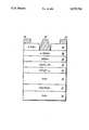
- FIGUREillustrates an enlarged, cross-sectional view of an embodiment of the present invention in an intermediate stage of fabrication.
- the FIGUREillustrates an enlarged, cross-sectional view of an embodiment of the present invention in an intermediate stage of fabrication.
- a semi-insulating GaAs substrate 10having an undoped AlAs/GaAs superlattice buffer layer 12 formed thereon.
- GaAs substrate 10is formed using standard crystal growing techniques well known in the art.
- the remaining layersare formed using deposition techniques, such as molecular beam epitaxy or metal organic vapor phase epitaxy, which are also well known in the art.
- the thickness of undoped AlAs/GaAs superlattice buffer layer 12is typically approximately 1,000 angstroms.
- An undoped GaAs layer 14typically of 2,000 angstroms, is thereafter formed on superlattice buffer layer 12.
- Undoped GaAs layer 14 and undoped AlAs/GaAs superlattice buffer layer 12are used to obtain good underlying characteristics for an In x Ga 1-x As channel layer 18 to be formed later in the process. Thus, undoped GaAs layer 14 and undoped AlAs/GaAs superlattice buffer layer 12 are not absolutely required in the present invention.
- An undoped GaAs y P 1-y layer 16is subsequently formed on 25 undoped GaAs layer 14. The undoped In x Ga 1-x As channel layer 18 is deposited over undoped GaAs y P 1-y layer 16.
- the deviceis further completed by standard processing by forming a spacer layer 20, shown as an undoped AlGaAs layer in this embodiment, on In x Ga 1-x As channel layer 18.
- An electron supplying layer 22, shown as an N-doped AlGaAs layer in this embodiment, and a capping layer 24, shown as N-doped GaAs layer in this embodiment,are formed on undoped AlGaAs layer 20.
- a portion of capping layer 24is removed in order to form a gate metal layer 28 on electron supplying layer 22.
- Source and drain regions 26are thereafter formed on capping layer 24, which provides for ohmic contact to source and drain regions 26.
- AlGaAs spacer layer 20, electron supplying layer 22, and capping layer 24are not essential to the completion of the embodiment shown here to form other types of FETs, however, electron supplying layer 22 is needed in order to form a high performance MODFET.
- Undoped GaAs y P 1-y layer 16acts as a stress-layer compensating for every y less than 1.
- GaAs y P 1-y layer 16acts as a stress-compensating layer because the lattice constant of GaAs y P 1-y layer 16 is less than the lattice constant of GaAs layer 14 or GaAs substrate 10 for y less than 1; while the lattice constant of In x Ga 1-x As channel layer 18 is larger than the lattice constant of GaAs layer 14 or GaAs substrate 10, for any x greater than 0.
- GaAs y P 1-y layer 16experiences a tensile strain in relation to GaAs substrate 10 in the plane parallel to the surface of GaAs substrate 10, while In x Ga 1-x As channel layer 18 experiences a compressive strain in relation to GaAs substrate 10 in the plane parallel to the surface of GaAs substrate 10. This means that the strain in GaAs y P 1-y layer 16 is opposite in sign to that in In x Ga 1-x As channel layer 18 and thus can act as a stress-compensating layer.
- the thickness and y of GaAs y P 1-y layer 16is chosen so that a pseudomorphic GaAs y P 1-y layer is formed.
- GaAs y P 1-y layer 16In order for the GaAs y P 1-y layer 16 to be a direct bandgap layer, y must be greater than 0.55. However, applications where carrier transport and/or optical recombination in undoped GaAs y P 1-y layer 16 are such that a direct bandgap layer is not required, a value of y less than 0.55 may also be used. With the use of undoped GaAs y P 1-y layer 16, x may be greater than 0.25 in In x Ga 1-x As channel layer 18 without having to compromise the thickness of this layer for device applications. Note that a graded GaAs y P 1-y layer 16 may be formed, however, it is not preferable from a manufacturing standpoint because it complicates the process.
- the choice of thickness and the value of x of In x Ga 1-x As channel layer 18is now less restricted by lattice mismatch considerations. Higher values of x can be chosen for enhanced transport properties.
- the conduction band discontinuity between In x Ga 1-x As channel layer 18 and GaAs y P 1-y layer 16is also significantly larger. This gives better electron confinement within In x Ga 1-x As channel layer 18 and thus improves device characteristics to provide a GaAs MODFET having high frequency and high speed performance.
Landscapes
- Junction Field-Effect Transistors (AREA)
- Recrystallisation Techniques (AREA)
- Crystals, And After-Treatments Of Crystals (AREA)
Abstract
Description
Claims (14)
Priority Applications (2)
| Application Number | Priority Date | Filing Date | Title |
|---|---|---|---|
| US07/620,819US5075744A (en) | 1990-12-03 | 1990-12-03 | GaAs heterostructure having a GaAsy P1-y stress-compensating layer |
| JP3332439AJP2620901B2 (en) | 1990-12-03 | 1991-11-21 | GaAs heterostructure with stress compensation layer |
Applications Claiming Priority (1)
| Application Number | Priority Date | Filing Date | Title |
|---|---|---|---|
| US07/620,819US5075744A (en) | 1990-12-03 | 1990-12-03 | GaAs heterostructure having a GaAsy P1-y stress-compensating layer |
Publications (1)
| Publication Number | Publication Date |
|---|---|
| US5075744Atrue US5075744A (en) | 1991-12-24 |
Family
ID=24487528
Family Applications (1)
| Application Number | Title | Priority Date | Filing Date |
|---|---|---|---|
| US07/620,819Expired - LifetimeUS5075744A (en) | 1990-12-03 | 1990-12-03 | GaAs heterostructure having a GaAsy P1-y stress-compensating layer |
Country Status (2)
| Country | Link |
|---|---|
| US (1) | US5075744A (en) |
| JP (1) | JP2620901B2 (en) |
Cited By (11)
| Publication number | Priority date | Publication date | Assignee | Title |
|---|---|---|---|---|
| US5719895A (en)* | 1996-09-25 | 1998-02-17 | Picolight Incorporated | Extended wavelength strained layer lasers having short period superlattices |
| US5719894A (en)* | 1996-09-25 | 1998-02-17 | Picolight Incorporated | Extended wavelength strained layer lasers having nitrogen disposed therein |
| US5825796A (en)* | 1996-09-25 | 1998-10-20 | Picolight Incorporated | Extended wavelength strained layer lasers having strain compensated layers |
| US6222208B1 (en)* | 1997-06-06 | 2001-04-24 | Oki Data Corporation | Light-emitting diode and light-emitting diode array |
| US20030203531A1 (en)* | 2001-05-09 | 2003-10-30 | Vitaly Shchukin | Defect-free semiconductor templates for epitaxial growth and method of making same |
| US6653166B2 (en) | 2001-05-09 | 2003-11-25 | Nsc-Nanosemiconductor Gmbh | Semiconductor device and method of making same |
| US20130193573A1 (en)* | 2012-01-27 | 2013-08-01 | Skyworks Solutions, Inc. | Methods of stress balancing in gallium arsenide wafer processing |
| RU2534447C1 (en)* | 2013-07-09 | 2014-11-27 | Открытое акционерное общество "Научно-производственное предприятие "Пульсар" | Pseudomorphic heterointerface modulation-doped field-effect transistor |
| US9093506B2 (en) | 2012-05-08 | 2015-07-28 | Skyworks Solutions, Inc. | Process for fabricating gallium arsenide devices with copper contact layer |
| US9530719B2 (en) | 2014-06-13 | 2016-12-27 | Skyworks Solutions, Inc. | Direct die solder of gallium arsenide integrated circuit dies and methods of manufacturing gallium arsenide wafers |
| GB2612372B (en)* | 2021-11-02 | 2024-11-06 | Iqe Plc | A layered structure |
Citations (6)
| Publication number | Priority date | Publication date | Assignee | Title |
|---|---|---|---|---|
| US4088515A (en)* | 1973-04-16 | 1978-05-09 | International Business Machines Corporation | Method of making semiconductor superlattices free of misfit dislocations |
| US4558336A (en)* | 1984-03-02 | 1985-12-10 | The United States Of America As Represented By The Secretary Of The Army | MBE Growth technique for matching superlattices grown on GaAs substrates |
| EP0178673A2 (en)* | 1984-10-17 | 1986-04-23 | Nec Corporation | Epitaxial layer structure grown on graded substrate and method of growing the same |
| JPS63284869A (en)* | 1987-05-18 | 1988-11-22 | Oki Electric Ind Co Ltd | Heterojunction field-effect semiconductor device |
| JPH01199474A (en)* | 1988-02-04 | 1989-08-10 | Matsushita Electric Ind Co Ltd | Heterojunction type field-effect transistor |
| US5016065A (en)* | 1988-11-04 | 1991-05-14 | Sharp Kabushiki Kaisha | Compound semiconductor substrate with InGaP layer |
- 1990
- 1990-12-03USUS07/620,819patent/US5075744A/ennot_activeExpired - Lifetime
- 1991
- 1991-11-21JPJP3332439Apatent/JP2620901B2/ennot_activeExpired - Fee Related
Patent Citations (6)
| Publication number | Priority date | Publication date | Assignee | Title |
|---|---|---|---|---|
| US4088515A (en)* | 1973-04-16 | 1978-05-09 | International Business Machines Corporation | Method of making semiconductor superlattices free of misfit dislocations |
| US4558336A (en)* | 1984-03-02 | 1985-12-10 | The United States Of America As Represented By The Secretary Of The Army | MBE Growth technique for matching superlattices grown on GaAs substrates |
| EP0178673A2 (en)* | 1984-10-17 | 1986-04-23 | Nec Corporation | Epitaxial layer structure grown on graded substrate and method of growing the same |
| JPS63284869A (en)* | 1987-05-18 | 1988-11-22 | Oki Electric Ind Co Ltd | Heterojunction field-effect semiconductor device |
| JPH01199474A (en)* | 1988-02-04 | 1989-08-10 | Matsushita Electric Ind Co Ltd | Heterojunction type field-effect transistor |
| US5016065A (en)* | 1988-11-04 | 1991-05-14 | Sharp Kabushiki Kaisha | Compound semiconductor substrate with InGaP layer |
Non-Patent Citations (4)
| Title |
|---|
| Chin et al., J. Vac Sci. Tech., B8 (2) Mar./Apr. 90, pp. 364 366, Achievement . . . Structure .* |
| Chin et al., J. Vac Sci. Tech., B8 (2) Mar./Apr. 90, pp. 364-366, "Achievement . . . Structure". |
| Smith et al., IEEE Electron Device Letters, vol. 10, No. 10, Oct. 89, "A 0.25 μm Gate-Length . . . 94 GHz", pp. 437-439. |
| Smith et al., IEEE Electron Device Letters, vol. 10, No. 10, Oct. 89, A 0.25 m Gate Length . . . 94 GHz , pp. 437 439.* |
Cited By (22)
| Publication number | Priority date | Publication date | Assignee | Title |
|---|---|---|---|---|
| US20050232323A1 (en)* | 1996-09-25 | 2005-10-20 | Picolight Incorporated | Extended wavelength strained layer lasers having nitrogen disposed therein |
| US7627014B2 (en) | 1996-09-25 | 2009-12-01 | Jds Uniphase Corporation | Extended wavelength strained layer lasers having nitrogen disposed therein |
| US5825796A (en)* | 1996-09-25 | 1998-10-20 | Picolight Incorporated | Extended wavelength strained layer lasers having strain compensated layers |
| US5960018A (en)* | 1996-09-25 | 1999-09-28 | Picolight Incorporated | Extended wavelength strained layer lasers having strain compensated layers |
| US6546031B1 (en) | 1996-09-25 | 2003-04-08 | Picolight Incorporated | Extended wavelength strained layer lasers having strain compensated layers |
| US5719895A (en)* | 1996-09-25 | 1998-02-17 | Picolight Incorporated | Extended wavelength strained layer lasers having short period superlattices |
| US5719894A (en)* | 1996-09-25 | 1998-02-17 | Picolight Incorporated | Extended wavelength strained layer lasers having nitrogen disposed therein |
| US6222208B1 (en)* | 1997-06-06 | 2001-04-24 | Oki Data Corporation | Light-emitting diode and light-emitting diode array |
| US7101444B2 (en) | 2001-05-09 | 2006-09-05 | Nl Nanosemiconductor Gmbh | Defect-free semiconductor templates for epitaxial growth |
| US20040087055A1 (en)* | 2001-05-09 | 2004-05-06 | Nsc-Nanosemiconductor Gmbh | Semiconductor device and method of making same |
| US6653166B2 (en) | 2001-05-09 | 2003-11-25 | Nsc-Nanosemiconductor Gmbh | Semiconductor device and method of making same |
| US20030203531A1 (en)* | 2001-05-09 | 2003-10-30 | Vitaly Shchukin | Defect-free semiconductor templates for epitaxial growth and method of making same |
| US6784074B2 (en) | 2001-05-09 | 2004-08-31 | Nsc-Nanosemiconductor Gmbh | Defect-free semiconductor templates for epitaxial growth and method of making same |
| US8900969B2 (en)* | 2012-01-27 | 2014-12-02 | Skyworks Solutions, Inc. | Methods of stress balancing in gallium arsenide wafer processing |
| US20130193573A1 (en)* | 2012-01-27 | 2013-08-01 | Skyworks Solutions, Inc. | Methods of stress balancing in gallium arsenide wafer processing |
| US9093506B2 (en) | 2012-05-08 | 2015-07-28 | Skyworks Solutions, Inc. | Process for fabricating gallium arsenide devices with copper contact layer |
| US10340186B2 (en) | 2012-05-08 | 2019-07-02 | Skyworks Solutions, Inc. | Method for reducing cross contamination in integrated circuit manufacturing |
| RU2534447C1 (en)* | 2013-07-09 | 2014-11-27 | Открытое акционерное общество "Научно-производственное предприятие "Пульсар" | Pseudomorphic heterointerface modulation-doped field-effect transistor |
| US9530719B2 (en) | 2014-06-13 | 2016-12-27 | Skyworks Solutions, Inc. | Direct die solder of gallium arsenide integrated circuit dies and methods of manufacturing gallium arsenide wafers |
| US9666508B2 (en) | 2014-06-13 | 2017-05-30 | Skyworks Solutions, Inc. | Gallium arsenide devices with copper backside for direct die solder attach |
| GB2612372B (en)* | 2021-11-02 | 2024-11-06 | Iqe Plc | A layered structure |
| US12408503B2 (en) | 2021-11-02 | 2025-09-02 | Iqe Plc | Layered structure with deformation control layer |
Also Published As
| Publication number | Publication date |
|---|---|
| JPH04268736A (en) | 1992-09-24 |
| JP2620901B2 (en) | 1997-06-18 |
Similar Documents
| Publication | Publication Date | Title |
|---|---|---|
| US4952527A (en) | Method of making buffer layers for III-V devices using solid phase epitaxy | |
| US9991172B2 (en) | Forming arsenide-based complementary logic on a single substrate | |
| US5770868A (en) | GaAs substrate with compositionally graded AlGaAsSb buffer for fabrication of high-indium fets | |
| US20080210927A1 (en) | Buffer architecture formed on a semiconductor wafer | |
| JP3224437B2 (en) | III-V compound semiconductor device | |
| US20010023942A1 (en) | Semiconductor device of heterojunction structure having quantum dot buffer layer | |
| US5075744A (en) | GaAs heterostructure having a GaAsy P1-y stress-compensating layer | |
| US5104825A (en) | Method of producing a semiconductor device | |
| US5907164A (en) | InAlAs/InGaAs heterojunction field effect type semiconductor device | |
| US6787826B1 (en) | Heterostructure field effect transistor | |
| US5550388A (en) | Heterojunction FET having barrier layer consisting of two layers between channel and buffer layers | |
| US5322808A (en) | Method of fabricating inverted modulation-doped heterostructure | |
| WO2007030316A2 (en) | Strain compensated high electron mobility transistor | |
| US7732836B2 (en) | Compound semiconductor epitaxial substrate and method for manufacturing the same | |
| US5571748A (en) | Methods for producing compound semiconductor devices | |
| JP2004221363A (en) | Epitaxial wafer for high-speed electron mobility transistor | |
| US5585306A (en) | Methods for producing compound semiconductor devices | |
| US9564525B2 (en) | Compound semiconductor device | |
| JP3158467B2 (en) | InAlAs / InGaAs heterojunction structure field effect transistor | |
| JP2808671B2 (en) | Field effect transistor | |
| JPH10284510A (en) | Semiconductor substrate | |
| JP2917719B2 (en) | Field effect transistor | |
| JPH088354B2 (en) | Heterojunction field effect transistor | |
| JP4770130B2 (en) | Epitaxial wafer for field effect transistor and epitaxial wafer for high electron mobility transistor | |
| JPH0695534B2 (en) | Heterostructure semiconductor device and manufacturing method thereof |
Legal Events
| Date | Code | Title | Description |
|---|---|---|---|
| AS | Assignment | Owner name:MOTOROLA, INC., ILLINOIS Free format text:ASSIGNMENT OF ASSIGNORS INTEREST.;ASSIGNOR:TSUI, RAYMOND K.;REEL/FRAME:005532/0001 Effective date:19901127 | |
| STCF | Information on status: patent grant | Free format text:PATENTED CASE | |
| CC | Certificate of correction | ||
| FPAY | Fee payment | Year of fee payment:4 | |
| FPAY | Fee payment | Year of fee payment:8 | |
| FPAY | Fee payment | Year of fee payment:12 | |
| AS | Assignment | Owner name:FREESCALE SEMICONDUCTOR, INC., TEXAS Free format text:ASSIGNMENT OF ASSIGNORS INTEREST;ASSIGNOR:MOTOROLA, INC.;REEL/FRAME:015698/0657 Effective date:20040404 Owner name:FREESCALE SEMICONDUCTOR, INC.,TEXAS Free format text:ASSIGNMENT OF ASSIGNORS INTEREST;ASSIGNOR:MOTOROLA, INC.;REEL/FRAME:015698/0657 Effective date:20040404 | |
| AS | Assignment | Owner name:CITIBANK, N.A. AS COLLATERAL AGENT, NEW YORK Free format text:SECURITY AGREEMENT;ASSIGNORS:FREESCALE SEMICONDUCTOR, INC.;FREESCALE ACQUISITION CORPORATION;FREESCALE ACQUISITION HOLDINGS CORP.;AND OTHERS;REEL/FRAME:018855/0129 Effective date:20061201 Owner name:CITIBANK, N.A. AS COLLATERAL AGENT,NEW YORK Free format text:SECURITY AGREEMENT;ASSIGNORS:FREESCALE SEMICONDUCTOR, INC.;FREESCALE ACQUISITION CORPORATION;FREESCALE ACQUISITION HOLDINGS CORP.;AND OTHERS;REEL/FRAME:018855/0129 Effective date:20061201 | |
| AS | Assignment | Owner name:CITIBANK, N.A., AS COLLATERAL AGENT,NEW YORK Free format text:SECURITY AGREEMENT;ASSIGNOR:FREESCALE SEMICONDUCTOR, INC.;REEL/FRAME:024397/0001 Effective date:20100413 Owner name:CITIBANK, N.A., AS COLLATERAL AGENT, NEW YORK Free format text:SECURITY AGREEMENT;ASSIGNOR:FREESCALE SEMICONDUCTOR, INC.;REEL/FRAME:024397/0001 Effective date:20100413 | |
| AS | Assignment | Owner name:FREESCALE SEMICONDUCTOR, INC., TEXAS Free format text:PATENT RELEASE;ASSIGNOR:CITIBANK, N.A., AS COLLATERAL AGENT;REEL/FRAME:037356/0553 Effective date:20151207 Owner name:FREESCALE SEMICONDUCTOR, INC., TEXAS Free format text:PATENT RELEASE;ASSIGNOR:CITIBANK, N.A., AS COLLATERAL AGENT;REEL/FRAME:037354/0225 Effective date:20151207 Owner name:FREESCALE SEMICONDUCTOR, INC., TEXAS Free format text:PATENT RELEASE;ASSIGNOR:CITIBANK, N.A., AS COLLATERAL AGENT;REEL/FRAME:037356/0143 Effective date:20151207 |