US5072288A - Microdynamic release structure - Google Patents
Microdynamic release structureDownload PDFInfo
- Publication number
- US5072288A US5072288AUS07/313,206US31320689AUS5072288AUS 5072288 AUS5072288 AUS 5072288AUS 31320689 AUS31320689 AUS 31320689AUS 5072288 AUS5072288 AUS 5072288A
- Authority
- US
- United States
- Prior art keywords
- beams
- substrate
- layer
- tungsten
- terminal end
- Prior art date
- Legal status (The legal status is an assumption and is not a legal conclusion. Google has not performed a legal analysis and makes no representation as to the accuracy of the status listed.)
- Expired - Lifetime
Links
Images


Classifications
- H—ELECTRICITY
- H02—GENERATION; CONVERSION OR DISTRIBUTION OF ELECTRIC POWER
- H02N—ELECTRIC MACHINES NOT OTHERWISE PROVIDED FOR
- H02N1/00—Electrostatic generators or motors using a solid moving electrostatic charge carrier
- H02N1/002—Electrostatic motors
- H02N1/006—Electrostatic motors of the gap-closing type
- H02N1/008—Laterally driven motors, e.g. of the comb-drive type
- B—PERFORMING OPERATIONS; TRANSPORTING
- B82—NANOTECHNOLOGY
- B82Y—SPECIFIC USES OR APPLICATIONS OF NANOSTRUCTURES; MEASUREMENT OR ANALYSIS OF NANOSTRUCTURES; MANUFACTURE OR TREATMENT OF NANOSTRUCTURES
- B82Y15/00—Nanotechnology for interacting, sensing or actuating, e.g. quantum dots as markers in protein assays or molecular motors
- H—ELECTRICITY
- H01—ELECTRIC ELEMENTS
- H01H—ELECTRIC SWITCHES; RELAYS; SELECTORS; EMERGENCY PROTECTIVE DEVICES
- H01H1/00—Contacts
- H01H1/0094—Switches making use of nanoelectromechanical systems [NEMS]
Definitions
- the present inventionrelates, in general, to a process for producing microdynamic structures and to the structures produced by that process, and more particularly is directed to the fabrication of three-dimensional tungsten cantilever beams on a substrate.
- micro-electromechanical systemsis a new, emerging technology which has as its goal the integration of electronic circuits, sensors, and electromechanical motion devices to build complete electromechanical systems on a micrometer scale.
- Recent research interest in such systemshas focused on the fabrication of microactuators and micromotors which have applications as micromechanical positioners, robotic actuators, and microprobes.
- Recent researchhas shown that rotating and sliding structures can be fabricated using modified silicon processing.
- research emphasishas been directed toward the fabrication of movable microstructures using polycrystalline silicon with sacrificial layers which, upon removal, releases the microstructures for motion.
- One disadvantage of the present technologyis that the deposition of only relatively thin layers of polysilicon are practical, and thus the silicon micromechanical structures are usually planar structures that are not easily extended to three dimensions. Furthermore, these structures are fragile and require many process steps to create a movable, free structure.
- Silicon-based electrostatic actuators and electrostatic motorsare crucial to the construction of integrated micro-electromechanical systems.
- attempts to achieve motion in microdeviceshave been impeded by the complexity of the processes required to build three dimensional structures, and by the forces that make materials stick together upon contact, to impede or prevent relative motion.
- Four major challenges to the production of a working micro motorhave been identified as being the control of friction and wear; the control of surface charges and interfacial forces; the development of a process that produces movable parts; and the control of stress, especially in the movable parts.
- the first two challengesrequire considerable experimental research to measure and identify the controlling parameters, while the third and fourth challenges are very closely related since a movable structure must conform to a designed shape, whereas stress plays a major role in distorting a structure when it is released from a mold.
- the present inventionis directed, in general, to a chemical vapor deposition (CVD) tungsten/silicon process for fabricating movable structures for electrostatic actuators and motors.
- the movable actuatoris fabricated on a suitable substrate such as a silicon chip, with careful attention being given to production of a structure which permits measurement of friction, stress, and electrostatic forces to enable the production of a stress-free device capable of mechanical motion under the control of applied electrostatic voltages.
- Thin films several micrometers in thicknesscan be deposited using chemical vapor deposition processes. Both CVD silicon dioxide and CVD tungsten processes have been developed with deposition rates of greater than 1,000 angstroms per minute. As described in U.S. Pat. No. 4,746,621 of David C. Thomas et al, assigned to the assignee of the present application, the disclosure of which is incorporated herein by reference, a selective tungsten on silicon process has been developed for producing patterned integrated circuit metal layers. This process uses patterned CVD silicon dioxide trenches which are ion implanted with silicon to make patterned tungsten microstructures.
- the CVD tungstenseeds only on the silicon implanted at the bottom of the trenches, and continues to grow vertically while filling the trenches from wall to wall. No anisotropic tungsten etch is required to produce high aspect ratio tungsten structures in accordance with that process.
- the present inventionis an extension of the selective tungsten CVD process described in the aforesaid U.S. Pat. No. 4,746,621 to produce stress-free cantilever beams that can be deflected using applied electric fields.
- a pair of beamsform the arms of microtweezers which can be deflected in both the X-Y plane, which is the plane of the two beams and which preferably is parallel to the plane of the substrate, and in the Z direction perpendicular to the substrate plane, by the application of potential differences between the tweezer arms or between the tweezer arms and the substrate, respectively.
- the application of such potential differencesproduces motion in the tweezer arms which is a function of the time during which the potentials are applied and which is a function of the magnitude of such potentials.
- a layer of low pressure CVD silicon dioxideis applied to a wafer coated with a thin silicon nitride layer, the latter layer serving to ensure insulation between the substrate and the tungsten beams produced by the process.
- a thin silicon nitride layeris deposited as an implantation mask on the top of the silicon dioxide layer and the mask is patterned to obtain vertical resist profiles.
- the channels for the tungsten beamsare then formed in the silicon dioxide layer by reactive ion etching. After the photoresist is removed, silicon atoms are implanted in the bottom of the channels. Thereafter, the silicon nitride mask is removed and a tungsten film is selectively deposited to fill the implanted oxide channels.
- An isolation maskis applied to etch the oxide surrounding the tungsten channels to thereby free the tungsten beams.
- the beamsare then covered with a conformal coating of CVD silicon dioxide to provide a thin insulating layer on the beams.
- the substratepreferably is silicon or gallium arsenide, it will be apparent that any substrate that can receive the thin silicon nitride and the CVD silicon dioxide layers can be used.
- the silicon or gallium arsenide substratesare preferred, however, when the microtweezers are to be incorporated into electronic circuitry such as VLSI circuits.
- the channelsare formed in an oxide layer which is formed over a polysilicon layer, which in turn is formed on the thin silicon nitride layer on the wafer.
- the channelsexpose the polysilicon layer, which then acts to seed the CVD tungsten which is deposited to form the tungsten beams.
- the cavity formed around the beamexposes the nitride layer under the beams to free them, as before, with the nitride layer remaining as an insulator on the top surface of the substrate.
- the substratemay be a silicon wafer formed by a Simox process, wherein a silicon substrate is covered by a thin layer of silicon dioxide which in turn is covered by a thin layer of silicon.
- This commercially available waferis then covered by an oxide layer such as CVD silicon dioxide, and trenches are formed therein, as discussed above. These trenches extend down to the thin layer of silicon, so that CVD tungsten will seed in the trenches without the need for ion implantation.
- a cavityis then formed around the beams to release them, as previously described.
- the tungsten beamsare extensions of the tungsten microcircuit conductors formed in a silicon dioxide layer, and extend in cantilever form from the silicon dioxide layer into the formed cavity.
- the beamsare elongated and are substantially square in cross-section, and extend substantially parallel to the floor of the cavity. Upon application of a potential across the beams, the beams move toward or away from each other, while application of a potential difference between a beam and the substrate will cause the beam to move toward or away from the substrate.
- tungsten beamshave been fabricated having a length of 200 micrometers, a height of 2.7 micrometers and a width of 2.5 micrometers. Such beams have been moved in a controlled manner by the application of selected voltages.
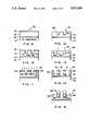
- FIG. 1is a perspective view of tungsten beams forming microtweezers in accordance with the present invention
- FIG. 2is a diagrammatic top view of the tweezers of FIG. 1;
- FIG. 3is a side view of the tweezers of FIG. 1;
- FIG. 4is an end view of one of the tweezer beams of FIG. 2;
- FIG. 5is a graphical depiction of the free end deflection of one tweezer arm as a function of the applied voltage between the tweezer arms of FIG. 1;
- FIG. 6is a graphical depiction of forced density distributions along the length of one tweezer arm
- FIG. 7is a graphical depiction of the dynamic beam deflection as a function of time for one tweezer arm
- FIG. 8is graphical depiction of the dynamic beam deflection as a function of position for one tweezer arm and for time;
- FIGS. 9 through 15illustrate the steps in a process of fabricating the tweezer of FIG. 1;
- FIGS. 16-20 and 21-25illustrate the steps in alternative fabrication processes.
- FIG. 1a segment 10 of a microcircuit incorporating a pair of three-dimensional cantilever beams 14 and 16 fabricated from a material such as tungsten in accordance with the present invention.
- the microcircuitis formed on a substrate or base 18 which in a preferred form of the invention is a silicon or a gallium arsenide wafer, but which may be any material capable of receiving an insulating layer 20 of, for example, silicon nitride.
- a layer of CVD silicon dioxide 22covers the layer 20, with the beams 14 and 16 being formed in a cavity 24 created in the silicon dioxide layer.
- the beamsare embedded in the silicon dioxide layer 22 at their near ends 26 and 28, respectively, and extend outwardly in a cantilever fashion from one face 29 of the cavity 24 with their far, or free ends 30 and 32, respectively, being suspended in the cavity and above the bottom surface 34 thereof.
- the beams 14 and 16lie in a common X-Y plane which may be parallel to the surface 34 and are free to move in this plane and in a Z direction perpendicular to the X-Y plane.
- the near ends of the beams 26 and 28are formed as a part of, and thus are connected to, metal circuit connector lines 36 and 38, respectively, in the illustrated embodiments.
- circuit linesmay lead, for example, to external contacts or other circuit components for supplying voltages to the respective beams 14 and 16 to thereby actuate the beams in a manner to be described.
- the two beams 14 and 16 in the illustrated embodimentcan be moved toward and away from each other upon application of appropriate voltages between the beams, and accordingly can perform the function of microtweezers.
- the beamsmay be formed of material exhibiting piezoelectric characteristics, so that motion of the beams by externally applied forces results in the generation of electrical signals which can be detected by the microcircuit to which the beams are connected.
- the beamsare generally rectangular in cross section and are capable of deflection through an angle ⁇ , with the deflection occurring over the full length L of the beam, and with the total motion away from the initial position defined by axis x being identified in FIG. 4 by u(x).
- this deflectionis shown in the X-Y plane, but it will be apparent that a similar deflection can also be produced in the Z direction.
- the length Lmay be 200 micrometers
- the width w of the beammay be about 2.5 micrometers
- the height h of the beammay be about 2.7 micrometers.
- the beams 14 and 16are rigidly fixed at their inner ends at cavity wall 29, which coincides with the axis y diagrammatically illustrated in FIG. 2, but are free to deflect over their entire length L.
- a step function potential differenceis applied between the arms 14 and 16, as by applying potentials to the lines 36 and 38, an attracting or repelling electrostatic force occurs between the charged arms, depending on the polarity of the potential.
- the armsact as electrodes, so the tweezers can be mathematically modeled as an air gap capacitor, and the distance between the two arms, d(x, t), is given by the following equation:
- Equation 2is an approximate expression to account for the fringing capacitance.
- the partial differential equation 4is replaced by a set of difference equations using the central difference scheme.
- the schemeis explicit and is stable when the temporal increment is sufficiently small compared with the spatial increment.
- the time dependent termsvanish, and the resulting ordinary differential equation can be replaced by a set of algebraic equations.
- curve 40illustrates the free end deflection of one tweezer arm as a function of the applied voltage between the two tweezer arms. As illustrated, for an applied voltage slightly above 112 volts, the deflection of the arm becomes unstable, and the tweezers close abruptly.
- FIG. 6illustrates the force density distribution along one arm of the tweezers due to an applied voltage of 112 volts.
- FIG. 7illustrates the dynamic beam deflection of one tweezer arm as a function of time and for positions along the beam upon application of a step input of 112 volts.
- the dynamic responseapproaches a steady state after a short time.
- the damped responsesare slower than the ones for the undamped case.
- the free ends for the undamped caseexhibit increased vibrational motion.
- FIG. 8shows the dynamic beam deflection as a function of the position for one tweezer arm over a period of time upon application of a step function of 112 volts.
- the foregoing simulations illustrated in FIGS. 5, 6, 7 and 8are for voltages applied between the tweezer arms 14 and 16 or between one arm and a nearby, horizontally spaced electrode, to produce motion in the X-Y plane parallel to surface 34.
- the arms 14 and 16can be deflected in a vertical direction by application of a suitable potential between a tweezer arm and a vertically spaced electrode such as the substrate 18. It has been found that the voltage required to cause one arm to touch the surface 34 is 117 volts when the arm is spaced above the surface 34 by a distance about equal to the thickness of the beam.
- These simulationsdescribe the threshold voltage behavior at which the tweezer arms make a sudden, unstable, large deflection. This threshold voltage is determined by the tweezer geometry and the mechanical properties of the material used to fabricate the arms 14 and 16. In the preferred form of the invention, and in the simulations discussed above, this material was a CVD tungsten material.
- the beams 14 and 16function as electrodes, and move upon the application of electrostatic forces therebetween, or between one of the beams and an adjacent electrode.
- the adjacent electrodemay be the substrate 18, while horizontal motion is produced using the two beams as electrodes. It will be understood, however, that a single beam may be provided, with an adjacent, nonmovable electrode also being provided to produce horizontal motion, if desired.
- the processing steps for the fabrication of a cantilever beamare based on the selective tungsten CVD technology described in U.S. Pat. No. 4,746,621.
- the processing sequenceis outlined in FIGS. 9 through 15, to which reference is now made.
- the starting materialis a substrate 18 which, for example, may be a three inch p-type silicon wafer.
- a silicon nitride layer 20is placed on the wafer 18 to provide insulation between the substrate and the released tungsten microtweezer beams 16 and 18.
- the layer 20is about 100 nm thick.
- a 100 nm thick silicon nitride layer 70is then deposited on the silicon dioxide layer 22 for use as an implantation mask, thereby providing a composite wafer 72 on which the microdynamic structure of the present invention may be formed, along with suitable VLSI electronic circuit components, if desired.
- a photoresist layer(not shown) is spun onto the top surface of the layer 70 and is exposed and developed in conventional manner to define a pattern for the channels in which the beams 14 and 16 are to be formed, and in which various interconnect lines may also be formed.
- a contrast enhancing material layer(not shown) is used with the photoresist for patterning to obtain vertical resist profiles.
- Channels 74 and 76are then formed through the patterned resist material on layer 70 into the silicon dioxide layer 22, as illustrated in FIG. 10. These channels are formed by reactive ion etching of the composite dielectric structure 72 in a CH 3 ambient.
- the oxide channels 74 and 76are etched to a depth of approximately 3.5 micrometers so that the bottom walls 78 and 80 of the channels are spaced above the top of layer 20 by about 2.5 micrometers. These channels may be parallel to each other, or may diverge or converge slightly, or may take other configurations as desired, with the channels serving as molds for the tungsten beams which are to be formed.
- silicon atoms at an energy of 40 KeVare implanted, as illustrated by the arrows 82 in FIG. 11.
- This stepproduces an implantation layer 84 in the bottom of channels 74 and 76, respectively, as well as on the silicon nitride layer 70.
- the silicon atomsare implanted at a dosage sufficient to initiate seeding of tungsten in the subsequent deposition step; for example, a silicon dosage of about 1 ⁇ 10 17 per square centimeter has been found to be sufficient to initiate the deposition of tungsten on silicon dioxide.
- the structure 72is then subjected to an oxygen plasma to remove any carbon contamination encountered during the implantation. To expose the peak silicon concentration in the implanted oxide channels, buffered HF is used. It has been found that as an alternative a polysilicon material can be implanted for seeding the deposition of tungsten.
- the silicon nitride layer 70is selectively removed in a hot phosphoric acid solution, taking with it any silicon implantation which might have occurred on that layer. This leaves the composite dielectric structure 72 with a planar top surface 88 and channels 74 and 76 which is ready to receive the tungsten material which is to form the beams 14 and 16.
- a tungsten filmis selectively deposited, as indicated by arrows 90, onto the composite structure 72 so as to fill the implanted oxide channels 74 and 76.
- the filmmay be deposited in a Genus 8432 cold wall reactor at a temperature of 580° C.
- the silicon layer 84 at the bottom of channels 74 and 76facilitates the deposition of the tungsten in the channels and ensures good adhesion of the tungsten material.
- the depositionis selective, since tungsten does not adhere to dielectric oxides, and thus will not adhere to the top surface 88 of the layer 22.
- the tungstenfills the channels completely to provide tungsten conductor structures 92, with the walls of the channels providing the molds for shaping the tungsten.
- the tungstenfills the channels completely to provide planar top surfaces which are level with the planar surface 88 of the wafer.
- an isolation mask 94is deposited on the top wall 88 of the wafer 72 to mask the beams, and the cavity 24 is etched in the silicon dioxide layer 22.
- This etching stepremoves the silicon dioxide material from around the beams 14 and 16 to release the beams, leaving the ends 26 and 28 embedded in the silicon dioxide material for support purposes (see FIG. 1), but allowing the length 1 of the beams 14 and 16 to extend outwardly from the wall 29 into the cavity 24.
- the beamsare spaced above the floor 34 of the channel and generally extend parallel to each other and to the channel floor.
- the silicon dioxide layerpreferably is removed down to the silicon nitride layer 20 to expose the top surface thereof, and the isolation mask layer 94 is then removed from the wafer 72.
- the resulting three-dimensional tungsten beamsare movable both horizontally and vertically, and the tungsten metal is substantially stress-free.
- this coatingis about 200 nm thick on each of the beams so that there will be a 400 nm insulating layer between the arms 14 and 16 when they come into contact.
- FIG. 1An alternative form of insulation between the two beams is illustrated in FIG. 1, where a pair of insulating pads 110 and 112 are provided on the opposing surfaces of the tip portions 30 and 32 of the beams 14 and 16. These pads may be of an oxide material which is left on the beam by appropriate masking during the step of removing the oxide material 22 during formation of cavity 24 (see FIGS. 13 and 14), or may be insulating material deposited on the beam tips by other suitable processes during the fabrication of the beam.
- the beamsmay be formed in accordance with the process illustrated in FIGS. 16-20 so as to facilitate production of beams having smooth bottom surfaces.
- a substrate 120such as a p-type silicon wafer is coated with a layer 122 of silicon nitride.
- This layer 122is then covered by a layer 123 of an oxide material such as silicon dioxide, which is then covered by a layer 124 of a polycrystalline silicon material, or polysilicon.
- This layer 124is, in turn, covered by a silicon dioxide layer 126 to produce a composite wafer structure 130.
- channels 132 and 134are etched through the layer 126, so that the bottom walls 136 and 138 of the channels are formed by the top surface of the polysilicon layer 124.
- Tungstenmay then be selectively deposited on the wafer 130, as indicated by arrows 140 in FIG. 18, thereby filling the channels to form the tungsten structures 142 and 144.
- the tungsten cantilever beams 146 and 148are released from the silicon dioxide layer 126 by etching a cavity 150 in the manner discussed above, with the cavity 150 extending through the polysilicon layer 124 and the silicon dioxide layer 123 to free the beams and to space the bottom surfaces 151 and 152 of the beams from the top surface of silicon nitride layer 122.
- the beamswill remain generally parallel to the bottom surface of the cavity, even after they have been freed from the silicon dioxide molds, so that, if desired, the layer 122 can also be removed from the cavity.
- the bottom surfaces 151 and 152 of the beamscontact the top surface of the polysilicon layer during formation of the beams and because this layer is relatively smooth ascompared to the surfaces 136 and 138 of the silicon implantation, the result is smoother bottom surfaces for the beams. Such smoother surfaces facilitate horizontal movement of the beams.
- the beamsmay be subjected to CVD silicon dioxide as illustrated by arrows 153 to produce a conformal insulating layer 154, as shown in FIG. 20, and as described with respect to FIG. 15.
- FIGS. 21-25A still further modification of the foregoing fabrication process is illustrated in FIGS. 21-25, and utilizes wafers produced by a recent technology for placing a single crystal silicon layer on an insulator.
- These wafersproduced by the Simox process, are commerically available, and consist of a silicon substrate 162, a silicon dioxide layer 164, and a thin single crystal silicon layer 166 (see FIG. 21).
- a second CVD silicon dioxide layer 168covers the crystal 166 to produce the composite wafer 170.
- channels 174 and 176are formed through the layer 168 in the manner previously described, with the bottom walls 178 and 180 of the channels being formed by the top surface of the crystalline layer 166.
- CVD tungstenis applied to the composite wafer, as previously described, and as shown by arrows 182 in FIG. 23, to fill the channels 174 and 176.
- the tungstenseeds on the silicon crystal 166 and fills the channels to form the tungsten structures 184 and 186.
- the structures 184 and 186are freed from the surrounding silicon dioxide material 168 by etching away the silicon dioxide layer 168, the underlying silicon crystal 166, and the silicon dioxide layer 164, for example through a mask 188, to form cavity 192, as illustrated in FIG. 24.
- the freed structuresform cantilever beams 190 and 192, with the bottom surfaces of the tungsten beams being spaced above the top surface of the silicon substrate 162. Thereafter, the beams may be provided with a CVD silicon dioxide coating 194, as illustrated in FIG. 25 and as previously described.
- the use of a silicon crystal layer 166provides a smooth bottom surface for the tungsten beams.
- a significant advantage of the CVD tungsten technology used in the fabrication of the cantilever beams described hereinis that multilayer devices can be made easily, since this technology provides planar top surfaces, as described in the aforesaid U.S. Pat. No. 4,746,621.
- the first tweezer designwas similar to that illustrated in FIG. 1, but with non-coated tungsten arms. This design was used to evaluate the accuracy of the simulated threshold voltages of 112 volts described hereinabove. However, because of the lack of insulation, that design could not be used for reliably repetitive closure of the tweezers, because tweezer closure produces electrical shorting and destruction of the device.
- the second tweezer designwas a composite beam in accordance with FIG. 1, but including the CVD silicon dioxide coating illustrated in FIG. 15. This coating prevented electrical shorting and produced a threshold voltage in the range of 135 to 155 volts.
- tungsten cantilever beamand selective chemical vapor deposition tungsten processes for fabricating such beams on a substrate.
- Two beamshave been formed to produce micromechanical tweezers that move in three dimensions when potential differences are applied between the tweezer arms to produce X-Y motion and between the tweezer arms and the silicon substrate to produce motion in the Z direction.
Landscapes
- Chemical & Material Sciences (AREA)
- Engineering & Computer Science (AREA)
- Nanotechnology (AREA)
- Health & Medical Sciences (AREA)
- Life Sciences & Earth Sciences (AREA)
- General Health & Medical Sciences (AREA)
- Molecular Biology (AREA)
- Crystallography & Structural Chemistry (AREA)
- Micromachines (AREA)
Abstract
Description
d(x,t)=d.sub.0 +2u(x,t), (Eq. 1)
Claims (23)
Priority Applications (2)
| Application Number | Priority Date | Filing Date | Title |
|---|---|---|---|
| US07/313,206US5072288A (en) | 1989-02-21 | 1989-02-21 | Microdynamic release structure |
| US07/762,492US5149673A (en) | 1989-02-21 | 1991-09-19 | Selective chemical vapor deposition of tungsten for microdynamic structures |
Applications Claiming Priority (1)
| Application Number | Priority Date | Filing Date | Title |
|---|---|---|---|
| US07/313,206US5072288A (en) | 1989-02-21 | 1989-02-21 | Microdynamic release structure |
Related Child Applications (1)
| Application Number | Title | Priority Date | Filing Date |
|---|---|---|---|
| US07/762,492DivisionUS5149673A (en) | 1989-02-21 | 1991-09-19 | Selective chemical vapor deposition of tungsten for microdynamic structures |
Publications (1)
| Publication Number | Publication Date |
|---|---|
| US5072288Atrue US5072288A (en) | 1991-12-10 |
Family
ID=23214785
Family Applications (1)
| Application Number | Title | Priority Date | Filing Date |
|---|---|---|---|
| US07/313,206Expired - LifetimeUS5072288A (en) | 1989-02-21 | 1989-02-21 | Microdynamic release structure |
Country Status (1)
| Country | Link |
|---|---|
| US (1) | US5072288A (en) |
Cited By (76)
| Publication number | Priority date | Publication date | Assignee | Title |
|---|---|---|---|---|
| US5130276A (en)* | 1991-05-16 | 1992-07-14 | Motorola Inc. | Method of fabricating surface micromachined structures |
| US5198390A (en)* | 1992-01-16 | 1993-03-30 | Cornell Research Foundation, Inc. | RIE process for fabricating submicron, silicon electromechanical structures |
| US5233224A (en)* | 1990-05-31 | 1993-08-03 | Canon Kabushiki Kaisha | Electrode having an improved configuration for a semiconductor element |
| US5293094A (en)* | 1989-09-08 | 1994-03-08 | Massachusetts Institute Of Technology | Miniature actuator |
| US5331236A (en)* | 1992-08-19 | 1994-07-19 | The United States Of America As Represented By The Secretary Of The Navy | Microdynamic devices fabricated on silicon-on-sapphire substrates |
| US5338997A (en)* | 1988-04-29 | 1994-08-16 | Fraunhofer Gesellschaft Zur Foerderung Der Angewandten Forschung E.V. | Micromanipulator for moving objects |
| WO1994018697A1 (en)* | 1993-02-04 | 1994-08-18 | Cornell Research Foundation, Inc. | Microstructures and single mask, single-crystal process for fabrication thereof |
| EP0592094A3 (en)* | 1992-09-21 | 1994-10-12 | Ibm | Micro-miniature structure fabrication. |
| US5363021A (en)* | 1993-07-12 | 1994-11-08 | Cornell Research Foundation, Inc. | Massively parallel array cathode |
| US5393375A (en)* | 1992-02-03 | 1995-02-28 | Cornell Research Foundation, Inc. | Process for fabricating submicron single crystal electromechanical structures |
| US5397904A (en)* | 1992-07-02 | 1995-03-14 | Cornell Research Foundation, Inc. | Transistor microstructure |
| US5399415A (en)* | 1993-02-05 | 1995-03-21 | Cornell Research Foundation, Inc. | Isolated tungsten microelectromechanical structures |
| US5426070A (en)* | 1993-05-26 | 1995-06-20 | Cornell Research Foundation, Inc. | Microstructures and high temperature isolation process for fabrication thereof |
| WO1995034917A1 (en)* | 1994-06-10 | 1995-12-21 | The Regents Of The University Of California | Cantilever pressure transducer |
| US5486337A (en)* | 1994-02-18 | 1996-01-23 | General Atomics | Device for electrostatic manipulation of droplets |
| US5536988A (en)* | 1993-06-01 | 1996-07-16 | Cornell Research Foundation, Inc. | Compound stage MEM actuator suspended for multidimensional motion |
| US5563343A (en)* | 1993-05-26 | 1996-10-08 | Cornell Research Foundation, Inc. | Microelectromechanical lateral accelerometer |
| US5610335A (en)* | 1993-05-26 | 1997-03-11 | Cornell Research Foundation | Microelectromechanical lateral accelerometer |
| US5627427A (en)* | 1991-12-09 | 1997-05-06 | Cornell Research Foundation, Inc. | Silicon tip field emission cathodes |
| US5640133A (en)* | 1995-06-23 | 1997-06-17 | Cornell Research Foundation, Inc. | Capacitance based tunable micromechanical resonators |
| US5712609A (en)* | 1994-06-10 | 1998-01-27 | Case Western Reserve University | Micromechanical memory sensor |
| US5856722A (en)* | 1996-01-02 | 1999-01-05 | Cornell Research Foundation, Inc. | Microelectromechanics-based frequency signature sensor |
| EP0890978A1 (en)* | 1997-07-10 | 1999-01-13 | STMicroelectronics S.r.l. | Process for manufacturing high-sensitivity capacitive and resonant integrated sensors, particularly accelerometers and gyroscopes, and relative sensors |
| WO1999004483A1 (en)* | 1997-07-16 | 1999-01-28 | Deutsches Zentrum für Luft- und Raumfahrt e.V. | Micromechanical device |
| US5914553A (en)* | 1997-06-16 | 1999-06-22 | Cornell Research Foundation, Inc. | Multistable tunable micromechanical resonators |
| US5943223A (en)* | 1997-10-15 | 1999-08-24 | Reliance Electric Industrial Company | Electric switches for reducing on-state power loss |
| US5949119A (en)* | 1995-07-13 | 1999-09-07 | Commissariat A L'energie Atomique | Device equipped with floating rigid microstructure elements |
| US6191518B1 (en)* | 1997-05-12 | 2001-02-20 | Nec Corporation | Microactuator and method of manufacturing the same |
| US6211598B1 (en)* | 1999-09-13 | 2001-04-03 | Jds Uniphase Inc. | In-plane MEMS thermal actuator and associated fabrication methods |
| US6290859B1 (en) | 1999-11-12 | 2001-09-18 | Sandia Corporation | Tungsten coating for improved wear resistance and reliability of microelectromechanical devices |
| US6407478B1 (en)* | 2000-08-21 | 2002-06-18 | Jds Uniphase Corporation | Switches and switching arrays that use microelectromechanical devices having one or more beam members that are responsive to temperature |
| KR100373739B1 (en)* | 2001-05-07 | 2003-02-26 | 조동일 | Method for Fabrication of Electrostatic Vertical Actuators Using One Single-crystalline Silicon Wafer |
| US6548938B2 (en)* | 2000-04-18 | 2003-04-15 | Viking Technologies, L.C. | Apparatus having a pair of opposing surfaces driven by a piezoelectric actuator |
| WO2003035543A1 (en)* | 2001-10-25 | 2003-05-01 | Micro Relay Holdings Pty Ltd | A method of fabrication of micro-devices |
| US6624730B2 (en)* | 2000-03-28 | 2003-09-23 | Tini Alloy Company | Thin film shape memory alloy actuated microrelay |
| US20030201654A1 (en)* | 2002-04-26 | 2003-10-30 | Ellis Matthew D. | Microgripper having linearly actuated grasping mechanisms |
| US6669454B2 (en)* | 2001-06-05 | 2003-12-30 | Wisconsin Alumni Research Foundation | Microfluidic actuation method and apparatus |
| US6679055B1 (en) | 2002-01-31 | 2004-01-20 | Zyvex Corporation | Electrothermal quadmorph microactuator |
| US6717332B2 (en) | 2000-04-18 | 2004-04-06 | Viking Technologies, L.C. | Apparatus having a support structure and actuator |
| US6759790B1 (en) | 2001-01-29 | 2004-07-06 | Viking Technologies, L.C. | Apparatus for moving folded-back arms having a pair of opposing surfaces in response to an electrical activation |
| US20040216988A1 (en)* | 2003-04-29 | 2004-11-04 | Rogier Receveur | Multi-stable micro electromechanical switches and methods of fabricating same |
| US6836056B2 (en) | 2000-02-04 | 2004-12-28 | Viking Technologies, L.C. | Linear motor having piezo actuators |
| US6870305B2 (en) | 2002-02-06 | 2005-03-22 | Viking Technologies, L.C. | Apparatus for moving a pair of opposing surfaces in response to an electrical activation |
| US6887732B2 (en) | 2001-05-07 | 2005-05-03 | Applied Materials, Inc. | Microstructure devices, methods of forming a microstructure device and a method of forming a MEMS device |
| US20050181636A1 (en)* | 2004-02-13 | 2005-08-18 | Zyvex Corporation | Sockets for microassembly |
| US20050199821A1 (en)* | 2004-03-12 | 2005-09-15 | Zyvex Corporation | Compact microcolumn for automated assembly |
| US20050199822A1 (en)* | 2004-03-12 | 2005-09-15 | Zyvex Corporation | Mems based charged particle deflector design |
| US20060181097A1 (en)* | 2004-11-12 | 2006-08-17 | Yoonsu Choi | Microfabricated mechanically actuated microtool and methods |
| US7096568B1 (en) | 2003-07-10 | 2006-08-29 | Zyvex Corporation | Method of manufacturing a microcomponent assembly |
| US20070228887A1 (en)* | 2006-03-31 | 2007-10-04 | Kabushiki Kaisha Toshiba | Piezoelectric driven mems device |
| US20070284969A1 (en)* | 2006-04-10 | 2007-12-13 | Honeywell International Inc. | Micromachined, piezoelectric vibration-induced energy harvesting device and its fabrication |
| US7314382B2 (en) | 2005-05-18 | 2008-01-01 | Zyvex Labs, Llc | Apparatus and methods of manufacturing and assembling microscale and nanoscale components and assemblies |
| CN100365510C (en)* | 2003-01-15 | 2008-01-30 | 友达光电股份有限公司 | Method for making metal pattern |
| US20080087841A1 (en)* | 2006-10-17 | 2008-04-17 | Zyvex Corporation | On-chip reflectron and ion optics |
| US7368856B2 (en) | 2003-04-04 | 2008-05-06 | Parker-Hannifin Corporation | Apparatus and process for optimizing work from a smart material actuator product |
| DE102006061386B3 (en)* | 2006-12-23 | 2008-06-19 | Atmel Germany Gmbh | Integrated assembly, its use and method of manufacture |
| KR100857313B1 (en) | 2006-07-18 | 2008-09-05 | 연세대학교 산학협력단 | Nano tweezers driven by electrostatic force and manufacturing method thereof |
| US7422403B1 (en) | 2003-10-23 | 2008-09-09 | Tini Alloy Company | Non-explosive releasable coupling device |
| US7441888B1 (en) | 2005-05-09 | 2008-10-28 | Tini Alloy Company | Eyeglass frame |
| US7540899B1 (en) | 2005-05-25 | 2009-06-02 | Tini Alloy Company | Shape memory alloy thin film, method of fabrication, and articles of manufacture |
| US7544257B2 (en) | 2004-05-06 | 2009-06-09 | Tini Alloy Company | Single crystal shape memory alloy devices and methods |
| US7586828B1 (en) | 2003-10-23 | 2009-09-08 | Tini Alloy Company | Magnetic data storage system |
| US20090314616A1 (en)* | 2006-01-20 | 2009-12-24 | Joachim Oberhammer | Swtich, Method and System For Switching The State of a Signal Path |
| US7763342B2 (en) | 2005-03-31 | 2010-07-27 | Tini Alloy Company | Tear-resistant thin film methods of fabrication |
| US7842143B2 (en) | 2007-12-03 | 2010-11-30 | Tini Alloy Company | Hyperelastic shape setting devices and fabrication methods |
| US8007674B2 (en) | 2007-07-30 | 2011-08-30 | Tini Alloy Company | Method and devices for preventing restenosis in cardiovascular stents |
| US20120182100A1 (en)* | 2011-01-19 | 2012-07-19 | Commissariat A L'energie Atomique Et Aux Energies Alternatives | Contactor and switch |
| US8349099B1 (en) | 2006-12-01 | 2013-01-08 | Ormco Corporation | Method of alloying reactive components |
| US8382917B2 (en) | 2007-12-03 | 2013-02-26 | Ormco Corporation | Hyperelastic shape setting devices and fabrication methods |
| US8556969B2 (en) | 2007-11-30 | 2013-10-15 | Ormco Corporation | Biocompatible copper-based single-crystal shape memory alloys |
| US8584767B2 (en) | 2007-01-25 | 2013-11-19 | Tini Alloy Company | Sprinkler valve with active actuation |
| US20130313946A1 (en)* | 2012-05-25 | 2013-11-28 | Electronics And Telecommunications Research Institute | Piezoelectric energy harvesting array and method of manufacturing the same |
| US8684101B2 (en) | 2007-01-25 | 2014-04-01 | Tini Alloy Company | Frangible shape memory alloy fire sprinkler valve actuator |
| US10124197B2 (en) | 2012-08-31 | 2018-11-13 | TiNi Allot Company | Fire sprinkler valve actuator |
| US11040230B2 (en) | 2012-08-31 | 2021-06-22 | Tini Alloy Company | Fire sprinkler valve actuator |
| WO2022109628A1 (en)* | 2020-11-23 | 2022-05-27 | Atom H2O, Llc | Systems and methods for plasma treatment enhanced leachability of tailings |
Citations (28)
| Publication number | Priority date | Publication date | Assignee | Title |
|---|---|---|---|---|
| US3039897A (en)* | 1958-04-09 | 1962-06-19 | Robert W Waring | Semiconductor and method of making the same |
| US3641373A (en)* | 1968-10-08 | 1972-02-08 | Proctor Ets | Electrostatic system for generating periodical mechanical vibrations |
| US3672985A (en)* | 1970-05-05 | 1972-06-27 | Westinghouse Electric Corp | Conductor elements spaced from microelectronic component surface and methods of making the same |
| US3761210A (en)* | 1971-07-09 | 1973-09-25 | Carborundum Co | Apparatus for producing fibers |
| US3835338A (en)* | 1973-08-23 | 1974-09-10 | A Martin | Electrically controlled ultra-micromanipulator |
| US4203128A (en)* | 1976-11-08 | 1980-05-13 | Wisconsin Alumni Research Foundation | Electrostatically deformable thin silicon membranes |
| JPS5710270A (en)* | 1980-06-20 | 1982-01-19 | Hitachi Ltd | Semiconductor capacitor type pressure sensor |
| US4319397A (en)* | 1979-07-10 | 1982-03-16 | Hitachi, Ltd. | Method of producing semiconductor displacement transducer |
| US4348650A (en)* | 1979-12-27 | 1982-09-07 | Clarion Co., Ltd. | Surface-acoustic-wave parametric device |
| GB2101404A (en)* | 1981-07-02 | 1983-01-12 | Standard Telephones Cables Ltd | Semiconductor switch device |
| US4381672A (en)* | 1981-03-04 | 1983-05-03 | The Bendix Corporation | Vibrating beam rotation sensor |
| US4516148A (en)* | 1982-08-30 | 1985-05-07 | The Board Of Trustees Of The Leland Stanford, Jr. University | Semiconductor device having improved lead attachment |
| US4517486A (en)* | 1984-02-21 | 1985-05-14 | The United States Of America As Represented By The Secretary Of The Army | Monolitic band-pass filter using piezoelectric cantilevers |
| US4570139A (en)* | 1984-12-14 | 1986-02-11 | Eaton Corporation | Thin-film magnetically operated micromechanical electric switching device |
| US4654555A (en)* | 1983-09-05 | 1987-03-31 | Omron Tateisi Electronics Co. | Multi pole piezoelectrically operating relay |
| US4697118A (en)* | 1986-08-15 | 1987-09-29 | General Electric Company | Piezoelectric switch |
| JPS62232171A (en)* | 1986-04-02 | 1987-10-12 | Nissan Motor Co Ltd | semiconductor acceleration sensor |
| US4706374A (en)* | 1984-10-19 | 1987-11-17 | Nissan Motor Co., Ltd. | Method of manufacture for semiconductor accelerometer |
| US4746621A (en)* | 1986-12-05 | 1988-05-24 | Cornell Research Foundation, Inc. | Planar tungsten interconnect |
| JPS63136982A (en)* | 1986-11-28 | 1988-06-09 | Canon Inc | Electrostatic actuator |
| US4754185A (en)* | 1986-10-16 | 1988-06-28 | American Telephone And Telegraph Company, At&T Bell Laboratories | Micro-electrostatic motor |
| US4772928A (en)* | 1985-04-27 | 1988-09-20 | Messerschmitt-Bolkow-Blohm Gmbh | Electric transducer for measuring mechanical quantities |
| US4776924A (en)* | 1986-10-02 | 1988-10-11 | Commissariat A L'energie Atomique | Process for the production of a piezoresistive gauge and to an accelerometer incorporating such a gauge |
| US4789803A (en)* | 1987-08-04 | 1988-12-06 | Sarcos, Inc. | Micropositioner systems and methods |
| US4805038A (en)* | 1987-07-30 | 1989-02-14 | Eastman Kodak Company | Imaging apparatus which includes a light-valve array having electrostatically deflectable elements |
| US4906840A (en)* | 1988-01-27 | 1990-03-06 | The Board Of Trustees Of Leland Stanford Jr., University | Integrated scanning tunneling microscope |
| US4956619A (en)* | 1988-02-19 | 1990-09-11 | Texas Instruments Incorporated | Spatial light modulator |
| US4959515A (en)* | 1984-05-01 | 1990-09-25 | The Foxboro Company | Micromechanical electric shunt and encoding devices made therefrom |
- 1989
- 1989-02-21USUS07/313,206patent/US5072288A/ennot_activeExpired - Lifetime
Patent Citations (29)
| Publication number | Priority date | Publication date | Assignee | Title |
|---|---|---|---|---|
| US3039897A (en)* | 1958-04-09 | 1962-06-19 | Robert W Waring | Semiconductor and method of making the same |
| US3641373A (en)* | 1968-10-08 | 1972-02-08 | Proctor Ets | Electrostatic system for generating periodical mechanical vibrations |
| US3769531A (en)* | 1968-10-08 | 1973-10-30 | Proctor Ets | Electrostatic system for generating periodical mechanical vibrations |
| US3672985A (en)* | 1970-05-05 | 1972-06-27 | Westinghouse Electric Corp | Conductor elements spaced from microelectronic component surface and methods of making the same |
| US3761210A (en)* | 1971-07-09 | 1973-09-25 | Carborundum Co | Apparatus for producing fibers |
| US3835338A (en)* | 1973-08-23 | 1974-09-10 | A Martin | Electrically controlled ultra-micromanipulator |
| US4203128A (en)* | 1976-11-08 | 1980-05-13 | Wisconsin Alumni Research Foundation | Electrostatically deformable thin silicon membranes |
| US4319397A (en)* | 1979-07-10 | 1982-03-16 | Hitachi, Ltd. | Method of producing semiconductor displacement transducer |
| US4348650A (en)* | 1979-12-27 | 1982-09-07 | Clarion Co., Ltd. | Surface-acoustic-wave parametric device |
| JPS5710270A (en)* | 1980-06-20 | 1982-01-19 | Hitachi Ltd | Semiconductor capacitor type pressure sensor |
| US4381672A (en)* | 1981-03-04 | 1983-05-03 | The Bendix Corporation | Vibrating beam rotation sensor |
| GB2101404A (en)* | 1981-07-02 | 1983-01-12 | Standard Telephones Cables Ltd | Semiconductor switch device |
| US4516148A (en)* | 1982-08-30 | 1985-05-07 | The Board Of Trustees Of The Leland Stanford, Jr. University | Semiconductor device having improved lead attachment |
| US4654555A (en)* | 1983-09-05 | 1987-03-31 | Omron Tateisi Electronics Co. | Multi pole piezoelectrically operating relay |
| US4517486A (en)* | 1984-02-21 | 1985-05-14 | The United States Of America As Represented By The Secretary Of The Army | Monolitic band-pass filter using piezoelectric cantilevers |
| US4959515A (en)* | 1984-05-01 | 1990-09-25 | The Foxboro Company | Micromechanical electric shunt and encoding devices made therefrom |
| US4706374A (en)* | 1984-10-19 | 1987-11-17 | Nissan Motor Co., Ltd. | Method of manufacture for semiconductor accelerometer |
| US4570139A (en)* | 1984-12-14 | 1986-02-11 | Eaton Corporation | Thin-film magnetically operated micromechanical electric switching device |
| US4772928A (en)* | 1985-04-27 | 1988-09-20 | Messerschmitt-Bolkow-Blohm Gmbh | Electric transducer for measuring mechanical quantities |
| JPS62232171A (en)* | 1986-04-02 | 1987-10-12 | Nissan Motor Co Ltd | semiconductor acceleration sensor |
| US4697118A (en)* | 1986-08-15 | 1987-09-29 | General Electric Company | Piezoelectric switch |
| US4776924A (en)* | 1986-10-02 | 1988-10-11 | Commissariat A L'energie Atomique | Process for the production of a piezoresistive gauge and to an accelerometer incorporating such a gauge |
| US4754185A (en)* | 1986-10-16 | 1988-06-28 | American Telephone And Telegraph Company, At&T Bell Laboratories | Micro-electrostatic motor |
| JPS63136982A (en)* | 1986-11-28 | 1988-06-09 | Canon Inc | Electrostatic actuator |
| US4746621A (en)* | 1986-12-05 | 1988-05-24 | Cornell Research Foundation, Inc. | Planar tungsten interconnect |
| US4805038A (en)* | 1987-07-30 | 1989-02-14 | Eastman Kodak Company | Imaging apparatus which includes a light-valve array having electrostatically deflectable elements |
| US4789803A (en)* | 1987-08-04 | 1988-12-06 | Sarcos, Inc. | Micropositioner systems and methods |
| US4906840A (en)* | 1988-01-27 | 1990-03-06 | The Board Of Trustees Of Leland Stanford Jr., University | Integrated scanning tunneling microscope |
| US4956619A (en)* | 1988-02-19 | 1990-09-11 | Texas Instruments Incorporated | Spatial light modulator |
Non-Patent Citations (8)
| Title |
|---|
| "Nanostructures for High Resolution Measurement of Magnetic Fields", IBM Tech. Disc. Bull., vol. 29, No. 1, 6/86. |
| Nanostructure for High Resolution Measurement of Magnetic Fields , IBM Tech. Disc. Bull., vol. 29, No. 1, 6/86.* |
| Petersen, "Micromechanical Light Deflector Array", IBM Technical Disclosure Bulletin, vol. 20, No. 1, Jun. 1977. |
| Petersen, Micromechanical Light Deflector Array , IBM Technical Disclosure Bulletin, vol. 20, No. 1, Jun. 1977.* |
| Sensors and Actuators, 11 1987, 189 206 W. S. N. Trimmer and K. J. Gabriel, AT&T Bell Laboratories.* |
| Sensors and Actuators, 11-1987, 189-206 W. S. N. Trimmer and K. J. Gabriel, AT&T Bell Laboratories. |
| Thick Film Resonant Device, vol. 9, No. 11, Apr. 1967, H. P. Hayden, IBM Technical Disclosure Bulletin.* |
| Thick-Film Resonant Device, vol. 9, No. 11, Apr. 1967, H. P. Hayden, IBM Technical Disclosure Bulletin. |
Cited By (114)
| Publication number | Priority date | Publication date | Assignee | Title |
|---|---|---|---|---|
| US5338997A (en)* | 1988-04-29 | 1994-08-16 | Fraunhofer Gesellschaft Zur Foerderung Der Angewandten Forschung E.V. | Micromanipulator for moving objects |
| US5293094A (en)* | 1989-09-08 | 1994-03-08 | Massachusetts Institute Of Technology | Miniature actuator |
| US5233224A (en)* | 1990-05-31 | 1993-08-03 | Canon Kabushiki Kaisha | Electrode having an improved configuration for a semiconductor element |
| US5130276A (en)* | 1991-05-16 | 1992-07-14 | Motorola Inc. | Method of fabricating surface micromachined structures |
| US5627427A (en)* | 1991-12-09 | 1997-05-06 | Cornell Research Foundation, Inc. | Silicon tip field emission cathodes |
| US5198390A (en)* | 1992-01-16 | 1993-03-30 | Cornell Research Foundation, Inc. | RIE process for fabricating submicron, silicon electromechanical structures |
| US5316979A (en)* | 1992-01-16 | 1994-05-31 | Cornell Research Foundation, Inc. | RIE process for fabricating submicron, silicon electromechanical structures |
| US5393375A (en)* | 1992-02-03 | 1995-02-28 | Cornell Research Foundation, Inc. | Process for fabricating submicron single crystal electromechanical structures |
| US5397904A (en)* | 1992-07-02 | 1995-03-14 | Cornell Research Foundation, Inc. | Transistor microstructure |
| US5331236A (en)* | 1992-08-19 | 1994-07-19 | The United States Of America As Represented By The Secretary Of The Navy | Microdynamic devices fabricated on silicon-on-sapphire substrates |
| EP0592094A3 (en)* | 1992-09-21 | 1994-10-12 | Ibm | Micro-miniature structure fabrication. |
| US5847454A (en)* | 1993-02-04 | 1998-12-08 | Cornell Research Foundcatton, Inc. | Electrically isolated released microstructures |
| US6051866A (en)* | 1993-02-04 | 2000-04-18 | Cornell Research Foundation, Inc. | Microstructures and single mask, single-crystal process for fabrication thereof |
| WO1994018697A1 (en)* | 1993-02-04 | 1994-08-18 | Cornell Research Foundation, Inc. | Microstructures and single mask, single-crystal process for fabrication thereof |
| US5846849A (en)* | 1993-02-04 | 1998-12-08 | Cornell Research Foundation, Inc. | Microstructure and single mask, single-crystal process for fabrication thereof |
| US5719073A (en)* | 1993-02-04 | 1998-02-17 | Cornell Research Foundation, Inc. | Microstructures and single mask, single-crystal process for fabrication thereof |
| US5399415A (en)* | 1993-02-05 | 1995-03-21 | Cornell Research Foundation, Inc. | Isolated tungsten microelectromechanical structures |
| US5426070A (en)* | 1993-05-26 | 1995-06-20 | Cornell Research Foundation, Inc. | Microstructures and high temperature isolation process for fabrication thereof |
| US5563343A (en)* | 1993-05-26 | 1996-10-08 | Cornell Research Foundation, Inc. | Microelectromechanical lateral accelerometer |
| US5610335A (en)* | 1993-05-26 | 1997-03-11 | Cornell Research Foundation | Microelectromechanical lateral accelerometer |
| US5536988A (en)* | 1993-06-01 | 1996-07-16 | Cornell Research Foundation, Inc. | Compound stage MEM actuator suspended for multidimensional motion |
| US5633552A (en)* | 1993-06-04 | 1997-05-27 | The Regents Of The University Of California | Cantilever pressure transducer |
| US5363021A (en)* | 1993-07-12 | 1994-11-08 | Cornell Research Foundation, Inc. | Massively parallel array cathode |
| US5486337A (en)* | 1994-02-18 | 1996-01-23 | General Atomics | Device for electrostatic manipulation of droplets |
| US5712609A (en)* | 1994-06-10 | 1998-01-27 | Case Western Reserve University | Micromechanical memory sensor |
| WO1995034917A1 (en)* | 1994-06-10 | 1995-12-21 | The Regents Of The University Of California | Cantilever pressure transducer |
| US5966066A (en)* | 1994-06-10 | 1999-10-12 | Case Western Reserve University | Micromechanical memory sensor |
| US5640133A (en)* | 1995-06-23 | 1997-06-17 | Cornell Research Foundation, Inc. | Capacitance based tunable micromechanical resonators |
| US5949119A (en)* | 1995-07-13 | 1999-09-07 | Commissariat A L'energie Atomique | Device equipped with floating rigid microstructure elements |
| US5856722A (en)* | 1996-01-02 | 1999-01-05 | Cornell Research Foundation, Inc. | Microelectromechanics-based frequency signature sensor |
| US7152300B1 (en) | 1997-05-12 | 2006-12-26 | Denso Corporation | Method of manufacturing a micromechanical structure |
| US6191518B1 (en)* | 1997-05-12 | 2001-02-20 | Nec Corporation | Microactuator and method of manufacturing the same |
| US5914553A (en)* | 1997-06-16 | 1999-06-22 | Cornell Research Foundation, Inc. | Multistable tunable micromechanical resonators |
| US6090638A (en)* | 1997-07-10 | 2000-07-18 | Stmicroelectronics S.R.L. | Process for manufacturing high-sensitivity capacitive and resonant integrated sensors, particularly accelerometers and gyroscopes, and sensors made therefrom |
| EP0890978A1 (en)* | 1997-07-10 | 1999-01-13 | STMicroelectronics S.r.l. | Process for manufacturing high-sensitivity capacitive and resonant integrated sensors, particularly accelerometers and gyroscopes, and relative sensors |
| US6184052B1 (en) | 1997-07-10 | 2001-02-06 | Stmicroelectronics, S.R.L. | Process for manufacturing high-sensitivity capacitive and resonant integrated sensors, particularly accelerometers and gyroscopes, and sensors made therefrom |
| WO1999004483A1 (en)* | 1997-07-16 | 1999-01-28 | Deutsches Zentrum für Luft- und Raumfahrt e.V. | Micromechanical device |
| US5943223A (en)* | 1997-10-15 | 1999-08-24 | Reliance Electric Industrial Company | Electric switches for reducing on-state power loss |
| US6211598B1 (en)* | 1999-09-13 | 2001-04-03 | Jds Uniphase Inc. | In-plane MEMS thermal actuator and associated fabrication methods |
| US6290859B1 (en) | 1999-11-12 | 2001-09-18 | Sandia Corporation | Tungsten coating for improved wear resistance and reliability of microelectromechanical devices |
| US6836056B2 (en) | 2000-02-04 | 2004-12-28 | Viking Technologies, L.C. | Linear motor having piezo actuators |
| US6624730B2 (en)* | 2000-03-28 | 2003-09-23 | Tini Alloy Company | Thin film shape memory alloy actuated microrelay |
| US7084726B2 (en)* | 2000-03-28 | 2006-08-01 | Tini Alloy Company | Thin film shape memory alloy actuated microrelay |
| US20040080239A1 (en)* | 2000-03-28 | 2004-04-29 | Vikas Gupta | Thin film shape memory alloy actuated microrelay |
| US6548938B2 (en)* | 2000-04-18 | 2003-04-15 | Viking Technologies, L.C. | Apparatus having a pair of opposing surfaces driven by a piezoelectric actuator |
| US6717332B2 (en) | 2000-04-18 | 2004-04-06 | Viking Technologies, L.C. | Apparatus having a support structure and actuator |
| US6737788B2 (en) | 2000-04-18 | 2004-05-18 | Viking Technologies, L.C. | Apparatus having a pair of opposing surfaces driven by a piezoelectric actuator |
| US6407478B1 (en)* | 2000-08-21 | 2002-06-18 | Jds Uniphase Corporation | Switches and switching arrays that use microelectromechanical devices having one or more beam members that are responsive to temperature |
| US6759790B1 (en) | 2001-01-29 | 2004-07-06 | Viking Technologies, L.C. | Apparatus for moving folded-back arms having a pair of opposing surfaces in response to an electrical activation |
| KR100373739B1 (en)* | 2001-05-07 | 2003-02-26 | 조동일 | Method for Fabrication of Electrostatic Vertical Actuators Using One Single-crystalline Silicon Wafer |
| US6887732B2 (en) | 2001-05-07 | 2005-05-03 | Applied Materials, Inc. | Microstructure devices, methods of forming a microstructure device and a method of forming a MEMS device |
| US6669454B2 (en)* | 2001-06-05 | 2003-12-30 | Wisconsin Alumni Research Foundation | Microfluidic actuation method and apparatus |
| WO2003035543A1 (en)* | 2001-10-25 | 2003-05-01 | Micro Relay Holdings Pty Ltd | A method of fabrication of micro-devices |
| US6679055B1 (en) | 2002-01-31 | 2004-01-20 | Zyvex Corporation | Electrothermal quadmorph microactuator |
| US6879087B2 (en) | 2002-02-06 | 2005-04-12 | Viking Technologies, L.C. | Apparatus for moving a pair of opposing surfaces in response to an electrical activation |
| US6870305B2 (en) | 2002-02-06 | 2005-03-22 | Viking Technologies, L.C. | Apparatus for moving a pair of opposing surfaces in response to an electrical activation |
| US6975061B2 (en) | 2002-02-06 | 2005-12-13 | Viking Technologies, L.C. | Apparatus for moving a pair of opposing surfaces in response to an electrical activation |
| US20030201654A1 (en)* | 2002-04-26 | 2003-10-30 | Ellis Matthew D. | Microgripper having linearly actuated grasping mechanisms |
| CN100365510C (en)* | 2003-01-15 | 2008-01-30 | 友达光电股份有限公司 | Method for making metal pattern |
| US7368856B2 (en) | 2003-04-04 | 2008-05-06 | Parker-Hannifin Corporation | Apparatus and process for optimizing work from a smart material actuator product |
| US7564171B2 (en) | 2003-04-04 | 2009-07-21 | Parker-Hannifin Corporation | Apparatus and process for optimizing work from a smart material actuator product |
| US8111118B2 (en) | 2003-04-29 | 2012-02-07 | Medtronic, Inc. | Multi-stable micro electromechanical switches and methods of fabricating same |
| US7688166B2 (en) | 2003-04-29 | 2010-03-30 | Medtronic, Inc. | Multi-stable micro electromechanical switches and methods of fabricating same |
| US20070009203A1 (en)* | 2003-04-29 | 2007-01-11 | Rogier Receveur | Multi-stable micro electromechanical switches and methods of fabricating same |
| US7190245B2 (en)* | 2003-04-29 | 2007-03-13 | Medtronic, Inc. | Multi-stable micro electromechanical switches and methods of fabricating same |
| US20040216988A1 (en)* | 2003-04-29 | 2004-11-04 | Rogier Receveur | Multi-stable micro electromechanical switches and methods of fabricating same |
| US7096568B1 (en) | 2003-07-10 | 2006-08-29 | Zyvex Corporation | Method of manufacturing a microcomponent assembly |
| US7586828B1 (en) | 2003-10-23 | 2009-09-08 | Tini Alloy Company | Magnetic data storage system |
| US7422403B1 (en) | 2003-10-23 | 2008-09-09 | Tini Alloy Company | Non-explosive releasable coupling device |
| US20050181636A1 (en)* | 2004-02-13 | 2005-08-18 | Zyvex Corporation | Sockets for microassembly |
| US7025619B2 (en) | 2004-02-13 | 2006-04-11 | Zyvex Corporation | Sockets for microassembly |
| US20050199821A1 (en)* | 2004-03-12 | 2005-09-15 | Zyvex Corporation | Compact microcolumn for automated assembly |
| US20050199822A1 (en)* | 2004-03-12 | 2005-09-15 | Zyvex Corporation | Mems based charged particle deflector design |
| US7544257B2 (en) | 2004-05-06 | 2009-06-09 | Tini Alloy Company | Single crystal shape memory alloy devices and methods |
| US7632361B2 (en) | 2004-05-06 | 2009-12-15 | Tini Alloy Company | Single crystal shape memory alloy devices and methods |
| US20060181097A1 (en)* | 2004-11-12 | 2006-08-17 | Yoonsu Choi | Microfabricated mechanically actuated microtool and methods |
| US20080284187A1 (en)* | 2004-11-12 | 2008-11-20 | Georgia Tech Research Corporation | Microfabricated mechanically actuated microtool and methods |
| US7461882B2 (en) | 2004-11-12 | 2008-12-09 | Georgia Tech Research Corp. | Microfabricated mechanically actuated microtool and methods |
| US7763342B2 (en) | 2005-03-31 | 2010-07-27 | Tini Alloy Company | Tear-resistant thin film methods of fabrication |
| US7441888B1 (en) | 2005-05-09 | 2008-10-28 | Tini Alloy Company | Eyeglass frame |
| US7314382B2 (en) | 2005-05-18 | 2008-01-01 | Zyvex Labs, Llc | Apparatus and methods of manufacturing and assembling microscale and nanoscale components and assemblies |
| US7540899B1 (en) | 2005-05-25 | 2009-06-02 | Tini Alloy Company | Shape memory alloy thin film, method of fabrication, and articles of manufacture |
| US20090314616A1 (en)* | 2006-01-20 | 2009-12-24 | Joachim Oberhammer | Swtich, Method and System For Switching The State of a Signal Path |
| US20070228887A1 (en)* | 2006-03-31 | 2007-10-04 | Kabushiki Kaisha Toshiba | Piezoelectric driven mems device |
| US7732990B2 (en)* | 2006-03-31 | 2010-06-08 | Kabushiki Kaisha Toshiba | Piezoelectric driven MEMS device |
| US20070284969A1 (en)* | 2006-04-10 | 2007-12-13 | Honeywell International Inc. | Micromachined, piezoelectric vibration-induced energy harvesting device and its fabrication |
| US7687977B2 (en)* | 2006-04-10 | 2010-03-30 | Honeywell International Inc. | Micromachined, piezoelectric vibration-induced energy harvesting device and its fabrication |
| KR100857313B1 (en) | 2006-07-18 | 2008-09-05 | 연세대학교 산학협력단 | Nano tweezers driven by electrostatic force and manufacturing method thereof |
| US7605377B2 (en) | 2006-10-17 | 2009-10-20 | Zyvex Corporation | On-chip reflectron and ion optics |
| US20080087841A1 (en)* | 2006-10-17 | 2008-04-17 | Zyvex Corporation | On-chip reflectron and ion optics |
| US10190199B2 (en) | 2006-12-01 | 2019-01-29 | Ormco Corporation | Method of alloying reactive components |
| US9340858B2 (en) | 2006-12-01 | 2016-05-17 | Ormco Corporation | Method of alloying reactive components |
| US8349099B1 (en) | 2006-12-01 | 2013-01-08 | Ormco Corporation | Method of alloying reactive components |
| US8685183B1 (en) | 2006-12-01 | 2014-04-01 | Ormco Corporation | Method of alloying reactive components |
| US20080217149A1 (en)* | 2006-12-23 | 2008-09-11 | Ulrich Schmid | Integrated arrangement and method for production |
| DE102006061386B3 (en)* | 2006-12-23 | 2008-06-19 | Atmel Germany Gmbh | Integrated assembly, its use and method of manufacture |
| US8584767B2 (en) | 2007-01-25 | 2013-11-19 | Tini Alloy Company | Sprinkler valve with active actuation |
| US8684101B2 (en) | 2007-01-25 | 2014-04-01 | Tini Alloy Company | Frangible shape memory alloy fire sprinkler valve actuator |
| US8007674B2 (en) | 2007-07-30 | 2011-08-30 | Tini Alloy Company | Method and devices for preventing restenosis in cardiovascular stents |
| US10610620B2 (en) | 2007-07-30 | 2020-04-07 | Monarch Biosciences, Inc. | Method and devices for preventing restenosis in cardiovascular stents |
| US8556969B2 (en) | 2007-11-30 | 2013-10-15 | Ormco Corporation | Biocompatible copper-based single-crystal shape memory alloys |
| US9539372B2 (en) | 2007-11-30 | 2017-01-10 | Ormco Corporation | Biocompatible copper-based single-crystal shape memory alloys |
| US7842143B2 (en) | 2007-12-03 | 2010-11-30 | Tini Alloy Company | Hyperelastic shape setting devices and fabrication methods |
| US8382917B2 (en) | 2007-12-03 | 2013-02-26 | Ormco Corporation | Hyperelastic shape setting devices and fabrication methods |
| US9127338B2 (en) | 2007-12-03 | 2015-09-08 | Ormco Corporation | Hyperelastic shape setting devices and fabrication methods |
| US20120182100A1 (en)* | 2011-01-19 | 2012-07-19 | Commissariat A L'energie Atomique Et Aux Energies Alternatives | Contactor and switch |
| US8531257B2 (en)* | 2011-01-19 | 2013-09-10 | Commissariat A L'energie Atomique Et Aux Energies Alternatives | Contactor and switch |
| US20160173006A1 (en)* | 2012-05-25 | 2016-06-16 | Electronics And Telecommunications Research Institute | Piezoelectric energy harvesting array and method of manufacturing the same |
| US9294015B2 (en)* | 2012-05-25 | 2016-03-22 | Electronics And Telecommunications Research Institute | Piezoelectric energy harvesting array and method of manufacturing the same |
| US9780698B2 (en)* | 2012-05-25 | 2017-10-03 | Electronics And Telecommunications Research Institute | Piezoelectric energy harvesting array and method of manufacturing the same |
| US20130313946A1 (en)* | 2012-05-25 | 2013-11-28 | Electronics And Telecommunications Research Institute | Piezoelectric energy harvesting array and method of manufacturing the same |
| US10124197B2 (en) | 2012-08-31 | 2018-11-13 | TiNi Allot Company | Fire sprinkler valve actuator |
| US11040230B2 (en) | 2012-08-31 | 2021-06-22 | Tini Alloy Company | Fire sprinkler valve actuator |
| WO2022109628A1 (en)* | 2020-11-23 | 2022-05-27 | Atom H2O, Llc | Systems and methods for plasma treatment enhanced leachability of tailings |
Similar Documents
| Publication | Publication Date | Title |
|---|---|---|
| US5072288A (en) | Microdynamic release structure | |
| US5149673A (en) | Selective chemical vapor deposition of tungsten for microdynamic structures | |
| US5179499A (en) | Multi-dimensional precision micro-actuator | |
| US5426070A (en) | Microstructures and high temperature isolation process for fabrication thereof | |
| MacDonald | SCREAM microelectromechanical systems | |
| JP3896158B2 (en) | Microstructure and single mask, single crystal process for its manufacture | |
| US6020272A (en) | Method for forming suspended micromechanical structures | |
| Shaw et al. | SCREAM I: a single mask, single-crystal silicon, reactive ion etching process for microelectromechanical structures | |
| US5479042A (en) | Micromachined relay and method of forming the relay | |
| Chen et al. | Selective chemical vapor deposition of tungsten for microdynamic structures | |
| US6130464A (en) | Latching microaccelerometer | |
| US20060157807A1 (en) | Three dimensional high aspect ratio micromachining | |
| US11186478B2 (en) | MEMS and method of manufacturing the same | |
| US6767614B1 (en) | Multiple-level actuators and clamping devices | |
| US9783407B2 (en) | Method for making a suspended membrane structure with buried electrode | |
| Jacobson et al. | Integrated force arrays: Theory and modeling of static operation | |
| Lee et al. | Multiple depth, single crystal silicon microactuators for large displacement fabricated by deep reactive ion etching | |
| Tas et al. | Design, fabrication and testing of laterally driven electrostatic motors employing walking motion and mechanical leverage | |
| US5489556A (en) | Method for the fabrication of electrostatic microswitches | |
| Fan | Integrated micromachinery: moving structures on silicon chips | |
| EP0491973B1 (en) | Integrated pneumatically and electrostatically controlled scanning tunneling microscope and method of making the same | |
| Gassend et al. | Precision in-plane hand assembly of bulk-microfabricated components for high-voltage MEMS arrays applications | |
| Hofmann et al. | Monolithic three-dimensional single-crystal silicon microelectromechanical systems | |
| JPH0852673A (en) | Ultra-small gripper with probe | |
| Gray et al. | Electrostatic actuators with expanded tuning range due to biaxial intrinsic stress gradients |
Legal Events
| Date | Code | Title | Description |
|---|---|---|---|
| AS | Assignment | Owner name:CORNELL RESEARCH FOUNDATION, INC., A CORP. OF NY, Free format text:ASSIGNMENT OF ASSIGNORS INTEREST.;ASSIGNORS:MAC DONALD, NOEL C.;CHEN, LIANG-YUH;ZHANG, ZUOYING L.;REEL/FRAME:005065/0276 Effective date:19890405 | |
| STCF | Information on status: patent grant | Free format text:PATENTED CASE | |
| FEPP | Fee payment procedure | Free format text:PAYOR NUMBER ASSIGNED (ORIGINAL EVENT CODE: ASPN); ENTITY STATUS OF PATENT OWNER: LARGE ENTITY Free format text:PAT HOLDER CLAIMS SMALL ENTITY STATUS - SMALL BUSINESS (ORIGINAL EVENT CODE: SM02); ENTITY STATUS OF PATENT OWNER: LARGE ENTITY | |
| FPAY | Fee payment | Year of fee payment:4 | |
| FEPP | Fee payment procedure | Free format text:PAT HLDR NO LONGER CLAIMS SMALL ENT STAT AS SMALL BUSINESS (ORIGINAL EVENT CODE: LSM2); ENTITY STATUS OF PATENT OWNER: LARGE ENTITY | |
| FPAY | Fee payment | Year of fee payment:8 | |
| AS | Assignment | Owner name:VENTURE LENDING & LEASING III, INC., AS AGENT, CAL Free format text:SECURITY AGREEMENT;ASSIGNOR:CALIENT OPTICAL COMPONENTS, INC.;REEL/FRAME:011934/0464 Effective date:20010516 | |
| AS | Assignment | Owner name:PENTECH FINANCIAL SERVICES, INC., CALIFORNIA Free format text:SECURITY INTEREST;ASSIGNOR:CALIENT OPTICAL COMPONENTS, INC.;REEL/FRAME:012252/0175 Effective date:20010516 | |
| FEPP | Fee payment procedure | Free format text:PAT HOLDER CLAIMS SMALL ENTITY STATUS, ENTITY STATUS SET TO SMALL (ORIGINAL EVENT CODE: LTOS); ENTITY STATUS OF PATENT OWNER: LARGE ENTITY | |
| FEPP | Fee payment procedure | Free format text:PAT HOLDER NO LONGER CLAIMS SMALL ENTITY STATUS, ENTITY STATUS SET TO UNDISCOUNTED (ORIGINAL EVENT CODE: STOL); ENTITY STATUS OF PATENT OWNER: LARGE ENTITY | |
| REFU | Refund | Free format text:REFUND - PAYMENT OF MAINTENANCE FEE, 12TH YR, SMALL ENTITY (ORIGINAL EVENT CODE: R2553); ENTITY STATUS OF PATENT OWNER: LARGE ENTITY | |
| FPAY | Fee payment | Year of fee payment:12 | |
| AS | Assignment | Owner name:CALIENT OPTICAL COMPONENTS, INC., NEW YORK Free format text:RELEASE AGREEMENT;ASSIGNORS:VENTURE LENDING;LEASING III, INC.;REEL/FRAME:016172/0341 Effective date:20040825 Owner name:CALIENT OPTICAL COMPONENTS, INC., NEW YORK Free format text:RELEASE AGREEMENT;ASSIGNOR:PENTECH FINANCIAL SERVICES, INC.;REEL/FRAME:016182/0031 Effective date:20040831 | |
| FEPP | Fee payment procedure | Free format text:PAYOR NUMBER ASSIGNED (ORIGINAL EVENT CODE: ASPN); ENTITY STATUS OF PATENT OWNER: LARGE ENTITY Free format text:PAYER NUMBER DE-ASSIGNED (ORIGINAL EVENT CODE: RMPN); ENTITY STATUS OF PATENT OWNER: LARGE ENTITY | |
| AS | Assignment | Owner name:NATIONAL SCIENCE FOUNDATION,VIRGINIA Free format text:CONFIRMATORY LICENSE;ASSIGNOR:CORNELL UNIVERSITY;REEL/FRAME:024401/0968 Effective date:19890425 |