US5070038A - Method of forming low-resistive contact to N+/P+ preohmic regions in very large scale integrated devices - Google Patents
Method of forming low-resistive contact to N+/P+ preohmic regions in very large scale integrated devicesDownload PDFInfo
- Publication number
- US5070038A US5070038AUS07/289,732US28973288AUS5070038AUS 5070038 AUS5070038 AUS 5070038AUS 28973288 AUS28973288 AUS 28973288AUS 5070038 AUS5070038 AUS 5070038A
- Authority
- US
- United States
- Prior art keywords
- layer
- preohmic
- titanium
- silicide
- regions
- Prior art date
- Legal status (The legal status is an assumption and is not a legal conclusion. Google has not performed a legal analysis and makes no representation as to the accuracy of the status listed.)
- Expired - Lifetime
Links
Images

Classifications
- H—ELECTRICITY
- H01—ELECTRIC ELEMENTS
- H01L—SEMICONDUCTOR DEVICES NOT COVERED BY CLASS H10
- H01L21/00—Processes or apparatus adapted for the manufacture or treatment of semiconductor or solid state devices or of parts thereof
- H01L21/70—Manufacture or treatment of devices consisting of a plurality of solid state components formed in or on a common substrate or of parts thereof; Manufacture of integrated circuit devices or of parts thereof
- H01L21/71—Manufacture of specific parts of devices defined in group H01L21/70
- H01L21/768—Applying interconnections to be used for carrying current between separate components within a device comprising conductors and dielectrics
- H01L21/76838—Applying interconnections to be used for carrying current between separate components within a device comprising conductors and dielectrics characterised by the formation and the after-treatment of the conductors
- H01L21/76886—Modifying permanently or temporarily the pattern or the conductivity of conductive members, e.g. formation of alloys, reduction of contact resistances
- H01L21/76889—Modifying permanently or temporarily the pattern or the conductivity of conductive members, e.g. formation of alloys, reduction of contact resistances by forming silicides of refractory metals
- H—ELECTRICITY
- H01—ELECTRIC ELEMENTS
- H01L—SEMICONDUCTOR DEVICES NOT COVERED BY CLASS H10
- H01L21/00—Processes or apparatus adapted for the manufacture or treatment of semiconductor or solid state devices or of parts thereof
- H01L21/02—Manufacture or treatment of semiconductor devices or of parts thereof
- H01L21/02104—Forming layers
- H01L21/02365—Forming inorganic semiconducting materials on a substrate
- H01L21/02612—Formation types
- H01L21/02617—Deposition types
- H01L21/02631—Physical deposition at reduced pressure, e.g. MBE, sputtering, evaporation
- H—ELECTRICITY
- H01—ELECTRIC ELEMENTS
- H01L—SEMICONDUCTOR DEVICES NOT COVERED BY CLASS H10
- H01L21/00—Processes or apparatus adapted for the manufacture or treatment of semiconductor or solid state devices or of parts thereof
- H01L21/02—Manufacture or treatment of semiconductor devices or of parts thereof
- H01L21/04—Manufacture or treatment of semiconductor devices or of parts thereof the devices having potential barriers, e.g. a PN junction, depletion layer or carrier concentration layer
- H01L21/18—Manufacture or treatment of semiconductor devices or of parts thereof the devices having potential barriers, e.g. a PN junction, depletion layer or carrier concentration layer the devices having semiconductor bodies comprising elements of Group IV of the Periodic Table or AIIIBV compounds with or without impurities, e.g. doping materials
- H01L21/28—Manufacture of electrodes on semiconductor bodies using processes or apparatus not provided for in groups H01L21/20 - H01L21/268
- H01L21/283—Deposition of conductive or insulating materials for electrodes conducting electric current
- H01L21/285—Deposition of conductive or insulating materials for electrodes conducting electric current from a gas or vapour, e.g. condensation
- H01L21/28506—Deposition of conductive or insulating materials for electrodes conducting electric current from a gas or vapour, e.g. condensation of conductive layers
- H01L21/28512—Deposition of conductive or insulating materials for electrodes conducting electric current from a gas or vapour, e.g. condensation of conductive layers on semiconductor bodies comprising elements of Group IV of the Periodic Table
- H01L21/28518—Deposition of conductive or insulating materials for electrodes conducting electric current from a gas or vapour, e.g. condensation of conductive layers on semiconductor bodies comprising elements of Group IV of the Periodic Table the conductive layers comprising silicides
- H—ELECTRICITY
- H01—ELECTRIC ELEMENTS
- H01L—SEMICONDUCTOR DEVICES NOT COVERED BY CLASS H10
- H01L21/00—Processes or apparatus adapted for the manufacture or treatment of semiconductor or solid state devices or of parts thereof
- H01L21/02—Manufacture or treatment of semiconductor devices or of parts thereof
- H01L21/04—Manufacture or treatment of semiconductor devices or of parts thereof the devices having potential barriers, e.g. a PN junction, depletion layer or carrier concentration layer
- H01L21/18—Manufacture or treatment of semiconductor devices or of parts thereof the devices having potential barriers, e.g. a PN junction, depletion layer or carrier concentration layer the devices having semiconductor bodies comprising elements of Group IV of the Periodic Table or AIIIBV compounds with or without impurities, e.g. doping materials
- H01L21/30—Treatment of semiconductor bodies using processes or apparatus not provided for in groups H01L21/20 - H01L21/26
- H01L21/31—Treatment of semiconductor bodies using processes or apparatus not provided for in groups H01L21/20 - H01L21/26 to form insulating layers thereon, e.g. for masking or by using photolithographic techniques; After treatment of these layers; Selection of materials for these layers
- H01L21/3205—Deposition of non-insulating-, e.g. conductive- or resistive-, layers on insulating layers; After-treatment of these layers
- H01L21/32051—Deposition of metallic or metal-silicide layers
- H01L21/32053—Deposition of metallic or metal-silicide layers of metal-silicide layers
- H—ELECTRICITY
- H01—ELECTRIC ELEMENTS
- H01L—SEMICONDUCTOR DEVICES NOT COVERED BY CLASS H10
- H01L21/00—Processes or apparatus adapted for the manufacture or treatment of semiconductor or solid state devices or of parts thereof
- H01L21/02—Manufacture or treatment of semiconductor devices or of parts thereof
- H01L21/04—Manufacture or treatment of semiconductor devices or of parts thereof the devices having potential barriers, e.g. a PN junction, depletion layer or carrier concentration layer
- H01L21/18—Manufacture or treatment of semiconductor devices or of parts thereof the devices having potential barriers, e.g. a PN junction, depletion layer or carrier concentration layer the devices having semiconductor bodies comprising elements of Group IV of the Periodic Table or AIIIBV compounds with or without impurities, e.g. doping materials
- H01L21/30—Treatment of semiconductor bodies using processes or apparatus not provided for in groups H01L21/20 - H01L21/26
- H01L21/31—Treatment of semiconductor bodies using processes or apparatus not provided for in groups H01L21/20 - H01L21/26 to form insulating layers thereon, e.g. for masking or by using photolithographic techniques; After treatment of these layers; Selection of materials for these layers
- H01L21/3205—Deposition of non-insulating-, e.g. conductive- or resistive-, layers on insulating layers; After-treatment of these layers
- H01L21/32055—Deposition of semiconductive layers, e.g. poly - or amorphous silicon layers
- H—ELECTRICITY
- H01—ELECTRIC ELEMENTS
- H01L—SEMICONDUCTOR DEVICES NOT COVERED BY CLASS H10
- H01L21/00—Processes or apparatus adapted for the manufacture or treatment of semiconductor or solid state devices or of parts thereof
- H01L21/70—Manufacture or treatment of devices consisting of a plurality of solid state components formed in or on a common substrate or of parts thereof; Manufacture of integrated circuit devices or of parts thereof
- H01L21/71—Manufacture of specific parts of devices defined in group H01L21/70
- H01L21/768—Applying interconnections to be used for carrying current between separate components within a device comprising conductors and dielectrics
- H01L21/76838—Applying interconnections to be used for carrying current between separate components within a device comprising conductors and dielectrics characterised by the formation and the after-treatment of the conductors
- H01L21/76877—Filling of holes, grooves or trenches, e.g. vias, with conductive material
- H—ELECTRICITY
- H01—ELECTRIC ELEMENTS
- H01L—SEMICONDUCTOR DEVICES NOT COVERED BY CLASS H10
- H01L23/00—Details of semiconductor or other solid state devices
- H01L23/52—Arrangements for conducting electric current within the device in operation from one component to another, i.e. interconnections, e.g. wires, lead frames
- H01L23/522—Arrangements for conducting electric current within the device in operation from one component to another, i.e. interconnections, e.g. wires, lead frames including external interconnections consisting of a multilayer structure of conductive and insulating layers inseparably formed on the semiconductor body
- H01L23/532—Arrangements for conducting electric current within the device in operation from one component to another, i.e. interconnections, e.g. wires, lead frames including external interconnections consisting of a multilayer structure of conductive and insulating layers inseparably formed on the semiconductor body characterised by the materials
- H01L23/53204—Conductive materials
- H01L23/53209—Conductive materials based on metals, e.g. alloys, metal silicides
- H01L23/53257—Conductive materials based on metals, e.g. alloys, metal silicides the principal metal being a refractory metal
- H—ELECTRICITY
- H01—ELECTRIC ELEMENTS
- H01L—SEMICONDUCTOR DEVICES NOT COVERED BY CLASS H10
- H01L23/00—Details of semiconductor or other solid state devices
- H01L23/52—Arrangements for conducting electric current within the device in operation from one component to another, i.e. interconnections, e.g. wires, lead frames
- H01L23/522—Arrangements for conducting electric current within the device in operation from one component to another, i.e. interconnections, e.g. wires, lead frames including external interconnections consisting of a multilayer structure of conductive and insulating layers inseparably formed on the semiconductor body
- H01L23/532—Arrangements for conducting electric current within the device in operation from one component to another, i.e. interconnections, e.g. wires, lead frames including external interconnections consisting of a multilayer structure of conductive and insulating layers inseparably formed on the semiconductor body characterised by the materials
- H01L23/53204—Conductive materials
- H01L23/53271—Conductive materials containing semiconductor material, e.g. polysilicon
- H—ELECTRICITY
- H01—ELECTRIC ELEMENTS
- H01L—SEMICONDUCTOR DEVICES NOT COVERED BY CLASS H10
- H01L2924/00—Indexing scheme for arrangements or methods for connecting or disconnecting semiconductor or solid-state bodies as covered by H01L24/00
- H01L2924/0001—Technical content checked by a classifier
- H01L2924/0002—Not covered by any one of groups H01L24/00, H01L24/00 and H01L2224/00
- Y—GENERAL TAGGING OF NEW TECHNOLOGICAL DEVELOPMENTS; GENERAL TAGGING OF CROSS-SECTIONAL TECHNOLOGIES SPANNING OVER SEVERAL SECTIONS OF THE IPC; TECHNICAL SUBJECTS COVERED BY FORMER USPC CROSS-REFERENCE ART COLLECTIONS [XRACs] AND DIGESTS
- Y10—TECHNICAL SUBJECTS COVERED BY FORMER USPC
- Y10S—TECHNICAL SUBJECTS COVERED BY FORMER USPC CROSS-REFERENCE ART COLLECTIONS [XRACs] AND DIGESTS
- Y10S148/00—Metal treatment
- Y10S148/019—Contacts of silicides
- Y—GENERAL TAGGING OF NEW TECHNOLOGICAL DEVELOPMENTS; GENERAL TAGGING OF CROSS-SECTIONAL TECHNOLOGIES SPANNING OVER SEVERAL SECTIONS OF THE IPC; TECHNICAL SUBJECTS COVERED BY FORMER USPC CROSS-REFERENCE ART COLLECTIONS [XRACs] AND DIGESTS
- Y10—TECHNICAL SUBJECTS COVERED BY FORMER USPC
- Y10S—TECHNICAL SUBJECTS COVERED BY FORMER USPC CROSS-REFERENCE ART COLLECTIONS [XRACs] AND DIGESTS
- Y10S148/00—Metal treatment
- Y10S148/026—Deposition thru hole in mask
- Y—GENERAL TAGGING OF NEW TECHNOLOGICAL DEVELOPMENTS; GENERAL TAGGING OF CROSS-SECTIONAL TECHNOLOGIES SPANNING OVER SEVERAL SECTIONS OF THE IPC; TECHNICAL SUBJECTS COVERED BY FORMER USPC CROSS-REFERENCE ART COLLECTIONS [XRACs] AND DIGESTS
- Y10—TECHNICAL SUBJECTS COVERED BY FORMER USPC
- Y10S—TECHNICAL SUBJECTS COVERED BY FORMER USPC CROSS-REFERENCE ART COLLECTIONS [XRACs] AND DIGESTS
- Y10S148/00—Metal treatment
- Y10S148/147—Silicides
Definitions
- the present inventionrelates to a method of forming low-resistive contact for using in very large scale intergrated (VLSI) devices, and more particularly, to a method of forming low-resistive contacts to N+ and/or P+ preohmic regions on a silicon substrate.
- VLSIvery large scale intergrated
- refractory metal silicideshave been used as interconnection materials to overcome disadvantages of a polycrystalline silicon (hereinafter referred to as polysilicon). Since the polysilicon has a sheet resistance of 20 to 30 ⁇ / ⁇ for a thickness of 5000 ⁇ , it is very difficulty to achieve the reduction of R-C delay time for a high speed operation and the scaling-down of line widths for higher density. Therefore, metal silicides such as tunsten silicide, titanium silicide, platnium silicide and tantalum silicide, which may provide a lower sheet resistance, by one order of magnitude, than that of the polysilicon, have been employed to achieve the scaling-down and the high speed operation in on-chip VLSI devices.
- metal silicidessuch as tunsten silicide, titanium silicide, platnium silicide and tantalum silicide, which may provide a lower sheet resistance, by one order of magnitude, than that of the polysilicon, have been employed to achieve the scaling-down and the high speed operation in on-chip
- a metal silicide capable of simultaneously making ohmic contacts with N+ and P+ preohmic regionsshould be selected.
- the tungsten silicidehas been used as a contract material for N+ preohmic regions.
- the tungsten silicideout-diffuses dopants from N+ and P+ preohmic regions during a silicidation process requiring high temperature treatment, the contact resistance between the tungsten silicide and the preohmic regions increases.
- sputter-deposited silicidesdo not always provide a good step coverage on vertical side-walls of the silicon dioxide, while metal silicides formed by chemical vapor deposition (CVD) generally have good step coverage thereon.
- CVDchemical vapor deposition
- the titanium silicide of metal silicideshas the lowest sheet resistance.
- Two methods of forming the titanium silicide by the sputtering technologyhave been known in the prior art. One is to thermally react sputter-deposited titanium with the underlying silicon. The other is to directly deposit the titanium silicide by sputtering. However, in any case, the sputter-deposited titanium may not provide a good step coverage on vertical side-walls of the silicon dioxide of about 5000 ⁇ in thickness and may cause a serious result of electrical disconnection.
- the method of forming low-resistive contacts to at least two preohmic regions formed in a silicon substrateincludes the steps of forming an insulating layer on the face of the silicon layer substrate, depositing a polyrcrystalline silicon on the insulating layer, forming holes having features of vertical side walls in the insulating layer and the polycrystalline silicon layer so that face portions of the preohmic regions are completely exposed, depositing a titanium layer on the polycrystalline silicon layer and the exposed preohmic regions, forming a titanium silicide layer so that the titanium reacts with the underlying silicon, and depositing a metal silicide layer on the titanium silicide layer and the side-walls of the insulating layer.
- the method of forming low-resistive contacts to at least two preohmic regions formed in a silicon substrateincludes the steps of forming an insulating layer on the face of the silicon substrate, forming holes having features of vertical side-walls in the insulating layer so that face portions of the preohmic regions are completely exposed, depositing a titanium silicide layer on the insulating layer and the exposed preohmic regions, and depositing a metal silicide layer on the titanium silicide layer and the side-walls of the insulating layer.
- the method of forming low-resistive contacts through holes in an insulating layer formed on the face of a silicon substrate to at least two preohmic regions exposed by the holes, said holes having substantially vertical side-walls in the insulating layerincludes the steps of depositing a polycrystalline silicon on the insulating layer, the side-walls of the holes and the exposed preohmic region, depositing a titanium layer on the face of the polycrystalline layer and the polycrystalline silicon layer above the exposed preohmic region, forming a titanium silicide layer so that the titanium reacts with the underlying polycrystalline silicon, and depositing a metal silicide layer on the titanium silicide and the side-walls of the polycrystalline silicon layer.
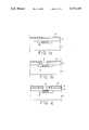
- FIG. 1a through FIG. 1dare cross-sectional views of portions of a silicon slice explaining a method of forming low-resistive contacts according to the present invention
- FIG. 1eis a cross-sectional view of a portion of a silicon slice showing another embodiment of the present invention.
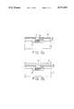
- FIG. 2a and FIG. 2bare cross-sectional views of portions of a silicon slice showing still another embodiment of the present invention.
- FIG. 1a through FIG. 1dthere are shown cross-sectional views of portions of a silicon slice in various processing steps according to an embodiment of the present invention.
- a preohmic region 2 in which N-type or P-type impurities are heavily dopedis formed on the face of a silicon substrate 1.
- a hole 5 exposing a selected surface area of the preohmic region 2is formed in the polysilicon layer 4 and the silicon dioxide layer 3 by an anisotropic eching technique such as RIE.
- the hole 5is about 0.6 ⁇ m in width.
- the silicon sliceis moved to magnetron sputtering machine to sputter titanium, and a native silicon dioxide and surface contaminations, on the polysilicon layer 4 and the exposed preohmic area 6' which are formed by the exposure of the ambient atmosphere, are eliminated by a sputter cleaning therein.
- the titanium layer 6of about 1000 ⁇ is sputter-deposited in an argon ambience.
- the thickness of a titanium layer 6is about 500 ⁇ on the polysilicon layer 4, although about 200 ⁇ on the exposed preohmic area (6') in the hole 5. But there is no deposited titanium on the vertical side-walls of the silicon dioxide layer 3.
- the silicon sliceis moved to a rapid thermal annealing (RTA) machine and heated at about 850° C. for about 10 seconds in a nitrogen ambience. By this heat treatment, the titanium is converted to a titanium silicide layer 7 by reacting with the underlying silicon layer 4 as shown in FIG. 1d.
- RTArapid thermal annealing
- a tungsten silicide layer 9is deposited at 360° C. by a well known low pressure chemical vapor deposition (LPCVD) on the titanium silicide layer 7 and the vertical side-wall (8) to prevent the electrical disconnection (i.e., electrical isolation) of the titanium silicide layer 7.
- LPCVDlow pressure chemical vapor deposition
- FIG. 1eAnother embodiment of the present invention is illustrated in FIG. 1e.
- a titanium silicide layer 10is formed by sputtering in the argon ambience from a titanium silicide target on the polysilicon layer 4 and the exposed preohmic area 6'.
- the thickness of the titanium silicide layer 10is about 1000 ⁇ on the polysilicon layer 4, although about 500 ⁇ on the exposed preohmic area 6'.
- the targetis of a silicon-rich titanium silicide having a titanium-silicon ratio of 1:2.6.
- a tungsten silicide layer 11is formed by LPCVD (i.e., by low pressure chemical vapor deposition) on the vertical side-wall 8 and the titanium silicide layer 10. Subsequently, an annealing heat treatment is performed at about 900° C. for about 20 seconds in the nitrogen ambient in the RTA machine to make the resistance of the silicide layers 10 and 11 low.
- LPCVDlow pressure chemical vapor deposition
- a N+ or P+ doped preohmic region 2is formed in the silicon substrate 1.
- a silicon dioxide layer 3is formed on the face of the silicon substrate 1 and then a hole 5 having a vertical side-wall 8 by the anisotropic eching technique is formed in the silicon dioxide layer 3 to expose a portion of the face of the preohmic region 2.
- a polysilicon layer 14is deposited by CVD.
- the thickness of the polysilicon layer 14is about 1000 ⁇ on the silicon dioxide layer 3, although about 500 ⁇ on the exposed preohmic area 6' and thinner on the side-wall 8.
- a titanium layer 15is sputter-deposited on the polysilicon layer 14.
- the thickness of the titanium layer 15 on the polysilicon layer 14is about 500 ⁇ , although about 200 ⁇ in the hole 5. But an electrical disconnection occurs on the side-wall 8.
- the silicidation processis performed by the heat treatment.
- a titanium silicide layer 16created by the silicidation process. But the electrical disconnection still remains. To prevent such electrical disconnection, a tungsten silicide layer 17 is deposited by the LPCVD on the side-wall 8 and the titanium silicide layer 16.
- Implantationmay be employed to prevent an increase of the contact resistance due to the out-diffusion of dopant from the preohmic region 2.
- Implantation processmay be peformed just before or just after the formation of the tungsten silicide layer 17.
- Implantation of the N+ preohmic regionis performed with arsenic, as, at the dose of about 10 16 /cm 2 , while that of the P+ preohmic region with boron, B, at the dose of about 10 16 /cm 2 .
- the tungsten silicidemay be a selected one of metal silicides formed at low temperature by the LPCVD. It is therefore to be understood that such modifications and embodiments are intended to fall within the spirit and scope of the appended claims.
Landscapes
- Engineering & Computer Science (AREA)
- Physics & Mathematics (AREA)
- Condensed Matter Physics & Semiconductors (AREA)
- General Physics & Mathematics (AREA)
- Computer Hardware Design (AREA)
- Microelectronics & Electronic Packaging (AREA)
- Power Engineering (AREA)
- Manufacturing & Machinery (AREA)
- Electrodes Of Semiconductors (AREA)
- Internal Circuitry In Semiconductor Integrated Circuit Devices (AREA)
- Semiconductor Integrated Circuits (AREA)
Abstract
Description
Claims (34)
Applications Claiming Priority (2)
| Application Number | Priority Date | Filing Date | Title |
|---|---|---|---|
| KR1019880017435AKR930004295B1 (en) | 1988-12-24 | 1988-12-24 | How to connect low resistance to N + and P + resistance area of VLSI device |
| KR1224 | 1988-12-24 |
Publications (1)
| Publication Number | Publication Date |
|---|---|
| US5070038Atrue US5070038A (en) | 1991-12-03 |
Family
ID=19280663
Family Applications (1)
| Application Number | Title | Priority Date | Filing Date |
|---|---|---|---|
| US07/289,732Expired - LifetimeUS5070038A (en) | 1988-12-24 | 1988-12-27 | Method of forming low-resistive contact to N+/P+ preohmic regions in very large scale integrated devices |
Country Status (6)
| Country | Link |
|---|---|
| US (1) | US5070038A (en) |
| JP (1) | JP2528961B2 (en) |
| KR (1) | KR930004295B1 (en) |
| DE (1) | DE3908676A1 (en) |
| FR (1) | FR2641126A1 (en) |
| GB (1) | GB2226446B (en) |
Cited By (15)
| Publication number | Priority date | Publication date | Assignee | Title |
|---|---|---|---|---|
| US5278096A (en)* | 1991-12-23 | 1994-01-11 | At&T Bell Laboratories | Transistor fabrication method |
| US5288664A (en)* | 1990-07-11 | 1994-02-22 | Fujitsu Ltd. | Method of forming wiring of semiconductor device |
| US5416034A (en)* | 1993-06-30 | 1995-05-16 | Sgs-Thomson Microelectronics, Inc. | Method of making resistor with silicon-rich silicide contacts for an integrated circuit |
| US5458697A (en)* | 1990-02-15 | 1995-10-17 | Kabushiki Kaisha Toshiba | Highly purified metal material and sputtering target using the same |
| US5565383A (en)* | 1993-12-03 | 1996-10-15 | Nec Corporation | Method for selective formation of silicide films without formation on vertical gate sidewalls using collimated sputtering |
| US5629218A (en)* | 1989-12-19 | 1997-05-13 | Texas Instruments Incorporated | Method for forming a field-effect transistor including a mask body and source/drain contacts |
| GB2319658A (en)* | 1996-09-21 | 1998-05-27 | United Microelectronics Corp | Method of fabricating a word line |
| US6048791A (en)* | 1998-03-31 | 2000-04-11 | Kabushiki Kaisha Toshiba | Semiconductor device with electrode formed of conductive layer consisting of polysilicon layer and metal-silicide layer and its manufacturing method |
| US6103606A (en)* | 1996-09-21 | 2000-08-15 | United Microelectronics Corp. | Method of fabricating a word line |
| US6200871B1 (en)* | 1994-08-30 | 2001-03-13 | Texas Instruments Incorporated | High performance self-aligned silicide process for sub-half-micron semiconductor technologies |
| US6495438B1 (en)* | 1999-08-30 | 2002-12-17 | Nec Corporation | Titanium polycide gate electrode and method of forming a titanium polycide gate electrode of a semiconductor device |
| US20060073639A1 (en)* | 2002-11-26 | 2006-04-06 | Shinko Electric Industries Co., Ltd. | Electronic parts packaging structure and method of manufacturing the same |
| EP1688998A3 (en)* | 1997-10-06 | 2006-11-15 | Canon Kabushiki Kaisha | Photoelectric conversion apparatus and image sensor |
| US20070001235A1 (en)* | 2005-06-29 | 2007-01-04 | Micron Technology, Inc. | Buried conductor for imagers |
| US7407882B1 (en) | 2004-08-27 | 2008-08-05 | Spansion Llc | Semiconductor component having a contact structure and method of manufacture |
Families Citing this family (3)
| Publication number | Priority date | Publication date | Assignee | Title |
|---|---|---|---|---|
| KR920010759A (en)* | 1990-11-16 | 1992-06-27 | 원본미기재 | How to manufacture low resistance contacts |
| EP0496169A1 (en)* | 1991-01-25 | 1992-07-29 | AT&T Corp. | Method of integrated circuit fabrication including filling windows with conducting material |
| KR100228619B1 (en)* | 1991-03-05 | 1999-11-01 | 아치 케이. 말론 | Method and Structure of Self-Mating Contact Formation |
Citations (9)
| Publication number | Priority date | Publication date | Assignee | Title |
|---|---|---|---|---|
| US4364166A (en)* | 1979-03-01 | 1982-12-21 | International Business Machines Corporation | Semiconductor integrated circuit interconnections |
| US4619035A (en)* | 1984-06-23 | 1986-10-28 | Nippon Gakki Seizo Kabushiki Kaisha | Method of manufacturing a semiconductor device including Schottky barrier diodes |
| US4720908A (en)* | 1984-07-11 | 1988-01-26 | Texas Instruments Incorporated | Process for making contacts and interconnects for holes having vertical sidewalls |
| JPS6377117A (en)* | 1986-09-19 | 1988-04-07 | Fujitsu Ltd | Manufacture 0f semiconductor device |
| US4751198A (en)* | 1985-09-11 | 1988-06-14 | Texas Instruments Incorporated | Process for making contacts and interconnections using direct-reacted silicide |
| US4784973A (en)* | 1987-08-24 | 1988-11-15 | Inmos Corporation | Semiconductor contact silicide/nitride process with control for silicide thickness |
| US4818723A (en)* | 1985-11-27 | 1989-04-04 | Advanced Micro Devices, Inc. | Silicide contact plug formation technique |
| US4897709A (en)* | 1988-04-15 | 1990-01-30 | Hitachi, Ltd. | Titanium nitride film in contact hole with large aspect ratio |
| US4904620A (en)* | 1987-04-08 | 1990-02-27 | U.S. Philips Corporation | Method of manufacturing a semiconductor device including a titanium disilicide contact |
Family Cites Families (17)
| Publication number | Priority date | Publication date | Assignee | Title |
|---|---|---|---|---|
| JPS57186341A (en)* | 1981-05-13 | 1982-11-16 | Hitachi Ltd | Semiconductor device |
| US4359490A (en)* | 1981-07-13 | 1982-11-16 | Fairchild Camera & Instrument Corp. | Method for LPCVD co-deposition of metal and silicon to form metal silicide |
| JPS59150421A (en)* | 1983-02-10 | 1984-08-28 | Toshiba Corp | Manufacture of semiconductor device |
| GB2139420B (en)* | 1983-05-05 | 1987-04-29 | Standard Telephones Cables Ltd | Semiconductor devices |
| US4545116A (en)* | 1983-05-06 | 1985-10-08 | Texas Instruments Incorporated | Method of forming a titanium disilicide |
| JPS60143648A (en)* | 1983-08-23 | 1985-07-29 | Nec Corp | Manufacture of semiconductor device |
| JPS60119750A (en)* | 1983-12-02 | 1985-06-27 | Hitachi Ltd | Manufacturing method of semiconductor device |
| JPS60193380A (en)* | 1984-03-15 | 1985-10-01 | Nec Corp | Manufacture of semiconductor device |
| JPS6158866A (en)* | 1984-08-30 | 1986-03-26 | 三菱マテリアル株式会社 | Manufacturing method of high melting point metal silicide matrix composite material |
| JPS61294816A (en)* | 1985-06-21 | 1986-12-25 | Matsushita Electronics Corp | Manufacture of semiconductor device |
| ATE46791T1 (en)* | 1985-07-29 | 1989-10-15 | Siemens Ag | METHOD FOR SELECTIVE FILLING OF CONTACT HOLES ETCHED IN INSULATING LAYERS WITH METALLIC CONDUCTIVE MATERIALS IN THE MANUFACTURE OF HIGHLY INTEGRATED SEMICONDUCTOR CIRCUITS AND A DEVICE FOR CARRYING OUT THE METHOD. |
| JPS62213277A (en)* | 1986-03-14 | 1987-09-19 | Nec Corp | Manufacture of semiconductor device |
| JPH0779136B2 (en)* | 1986-06-06 | 1995-08-23 | 株式会社日立製作所 | Semiconductor device |
| JPS63116A (en)* | 1986-06-19 | 1988-01-05 | Matsushita Electric Ind Co Ltd | Manufacture of semiconductor device |
| JPS63120419A (en)* | 1986-11-10 | 1988-05-24 | Matsushita Electronics Corp | Manufacture of semiconductor device |
| JPH06276518A (en)* | 1993-03-22 | 1994-09-30 | Sony Corp | Picture processor |
| JPH06321829A (en)* | 1993-05-07 | 1994-11-22 | Taiho Yakuhin Kogyo Kk | Alpha,alpha-dimethylcyclohexanecarbinol derivative or its salt |
- 1988
- 1988-12-24KRKR1019880017435Apatent/KR930004295B1/ennot_activeExpired - Lifetime
- 1988-12-27USUS07/289,732patent/US5070038A/ennot_activeExpired - Lifetime
- 1989
- 1989-02-02JPJP1022748Apatent/JP2528961B2/ennot_activeExpired - Lifetime
- 1989-03-16DEDE3908676Apatent/DE3908676A1/ennot_activeCeased
- 1989-05-17FRFR8906415Apatent/FR2641126A1/enactiveGranted
- 1989-09-22GBGB8921421Apatent/GB2226446B/ennot_activeExpired - Lifetime
Patent Citations (9)
| Publication number | Priority date | Publication date | Assignee | Title |
|---|---|---|---|---|
| US4364166A (en)* | 1979-03-01 | 1982-12-21 | International Business Machines Corporation | Semiconductor integrated circuit interconnections |
| US4619035A (en)* | 1984-06-23 | 1986-10-28 | Nippon Gakki Seizo Kabushiki Kaisha | Method of manufacturing a semiconductor device including Schottky barrier diodes |
| US4720908A (en)* | 1984-07-11 | 1988-01-26 | Texas Instruments Incorporated | Process for making contacts and interconnects for holes having vertical sidewalls |
| US4751198A (en)* | 1985-09-11 | 1988-06-14 | Texas Instruments Incorporated | Process for making contacts and interconnections using direct-reacted silicide |
| US4818723A (en)* | 1985-11-27 | 1989-04-04 | Advanced Micro Devices, Inc. | Silicide contact plug formation technique |
| JPS6377117A (en)* | 1986-09-19 | 1988-04-07 | Fujitsu Ltd | Manufacture 0f semiconductor device |
| US4904620A (en)* | 1987-04-08 | 1990-02-27 | U.S. Philips Corporation | Method of manufacturing a semiconductor device including a titanium disilicide contact |
| US4784973A (en)* | 1987-08-24 | 1988-11-15 | Inmos Corporation | Semiconductor contact silicide/nitride process with control for silicide thickness |
| US4897709A (en)* | 1988-04-15 | 1990-01-30 | Hitachi, Ltd. | Titanium nitride film in contact hole with large aspect ratio |
Cited By (23)
| Publication number | Priority date | Publication date | Assignee | Title |
|---|---|---|---|---|
| US5629218A (en)* | 1989-12-19 | 1997-05-13 | Texas Instruments Incorporated | Method for forming a field-effect transistor including a mask body and source/drain contacts |
| US5458697A (en)* | 1990-02-15 | 1995-10-17 | Kabushiki Kaisha Toshiba | Highly purified metal material and sputtering target using the same |
| US5679983A (en)* | 1990-02-15 | 1997-10-21 | Kabushiki Kaisha Toshiba | Highly purified metal material and sputtering target using the same |
| US5288664A (en)* | 1990-07-11 | 1994-02-22 | Fujitsu Ltd. | Method of forming wiring of semiconductor device |
| US5278096A (en)* | 1991-12-23 | 1994-01-11 | At&T Bell Laboratories | Transistor fabrication method |
| US6188112B1 (en) | 1993-06-30 | 2001-02-13 | Stmicroelectronics, Inc. | High impedance load for integrated circuit devices |
| US5416034A (en)* | 1993-06-30 | 1995-05-16 | Sgs-Thomson Microelectronics, Inc. | Method of making resistor with silicon-rich silicide contacts for an integrated circuit |
| US5565383A (en)* | 1993-12-03 | 1996-10-15 | Nec Corporation | Method for selective formation of silicide films without formation on vertical gate sidewalls using collimated sputtering |
| US6200871B1 (en)* | 1994-08-30 | 2001-03-13 | Texas Instruments Incorporated | High performance self-aligned silicide process for sub-half-micron semiconductor technologies |
| GB2319658A (en)* | 1996-09-21 | 1998-05-27 | United Microelectronics Corp | Method of fabricating a word line |
| US6103606A (en)* | 1996-09-21 | 2000-08-15 | United Microelectronics Corp. | Method of fabricating a word line |
| GB2319658B (en)* | 1996-09-21 | 2001-08-22 | United Microelectronics Corp | Method of fabricating a word line |
| EP1688998A3 (en)* | 1997-10-06 | 2006-11-15 | Canon Kabushiki Kaisha | Photoelectric conversion apparatus and image sensor |
| US6048791A (en)* | 1998-03-31 | 2000-04-11 | Kabushiki Kaisha Toshiba | Semiconductor device with electrode formed of conductive layer consisting of polysilicon layer and metal-silicide layer and its manufacturing method |
| US6495438B1 (en)* | 1999-08-30 | 2002-12-17 | Nec Corporation | Titanium polycide gate electrode and method of forming a titanium polycide gate electrode of a semiconductor device |
| US20060073639A1 (en)* | 2002-11-26 | 2006-04-06 | Shinko Electric Industries Co., Ltd. | Electronic parts packaging structure and method of manufacturing the same |
| US7530163B2 (en)* | 2002-11-26 | 2009-05-12 | Shinko Electric Industries Co., Ltd. | Electronic parts packaging structure and method of manufacturing the same |
| US7407882B1 (en) | 2004-08-27 | 2008-08-05 | Spansion Llc | Semiconductor component having a contact structure and method of manufacture |
| US20070001235A1 (en)* | 2005-06-29 | 2007-01-04 | Micron Technology, Inc. | Buried conductor for imagers |
| WO2007005267A1 (en)* | 2005-06-29 | 2007-01-11 | Micron Technology, Inc. | Buried conductor for imagers |
| US20070200181A1 (en)* | 2005-06-29 | 2007-08-30 | Rhodes Howard E | Buried conductor for imagers |
| US7842523B2 (en) | 2005-06-29 | 2010-11-30 | Micron Technology, Inc. | Buried conductor for imagers |
| US8018015B2 (en) | 2005-06-29 | 2011-09-13 | Micron Technology, Inc. | Buried conductor for imagers |
Also Published As
| Publication number | Publication date |
|---|---|
| DE3908676A1 (en) | 1990-06-28 |
| KR930004295B1 (en) | 1993-05-22 |
| GB8921421D0 (en) | 1989-11-08 |
| FR2641126B1 (en) | 1992-11-27 |
| GB2226446B (en) | 1993-02-24 |
| GB2226446A (en) | 1990-06-27 |
| FR2641126A1 (en) | 1990-06-29 |
| KR900010993A (en) | 1990-07-11 |
| JP2528961B2 (en) | 1996-08-28 |
| JPH02194524A (en) | 1990-08-01 |
Similar Documents
| Publication | Publication Date | Title |
|---|---|---|
| US5070038A (en) | Method of forming low-resistive contact to N+/P+ preohmic regions in very large scale integrated devices | |
| US5047367A (en) | Process for formation of a self aligned titanium nitride/cobalt silicide bilayer | |
| US6562718B1 (en) | Process for forming fully silicided gates | |
| JP3285934B2 (en) | Method for manufacturing semiconductor device | |
| JP3132750B2 (en) | Multilayer structure, semiconductor structure, capacitor of semiconductor device, method of preventing oxidation of silicon structure, and method of preventing diffusion of dopant | |
| US5874342A (en) | Process for forming MOS device in integrated circuit structure using cobalt silicide contacts as implantation media | |
| EP0800204B1 (en) | A process for device fabrication in which a thin layer of cobalt silicide is formed | |
| JP2819240B2 (en) | Method of manufacturing MOS transistor having source / drain regions and silicide with shallow junction | |
| EP0219827B1 (en) | Improved process for forming low sheet resistance metal silicide layers on semiconductor substrates | |
| US6451693B1 (en) | Double silicide formation in polysicon gate without silicide in source/drain extensions | |
| US5739064A (en) | Second implanted matrix for agglomeration control and thermal stability | |
| US6238986B1 (en) | Formation of junctions by diffusion from a doped film at silicidation | |
| JP2720827B2 (en) | Method for manufacturing semiconductor device | |
| KR19980053694A (en) | How to make MOSFET | |
| US6096599A (en) | Formation of junctions by diffusion from a doped film into and through a silicide during silicidation | |
| US6277721B1 (en) | Salicide formation process | |
| US6090645A (en) | Fabrication method of semiconductor device with gettering treatment | |
| US5963829A (en) | Method of forming silicide film | |
| US6291890B1 (en) | Semiconductor device having a silicide structure | |
| KR100289372B1 (en) | A method of forming polycide | |
| US6169005B1 (en) | Formation of junctions by diffusion from a doped amorphous silicon film during silicidation | |
| JP2586407B2 (en) | Method for manufacturing semiconductor device | |
| EP0137980B1 (en) | Method for making electrical connections to a semiconductor substrate | |
| CA1235824A (en) | Vlsi mosfet circuits using refractory metal and/or refractory metal silicide | |
| JP4011434B2 (en) | Semiconductor device manufacturing method and semiconductor device |
Legal Events
| Date | Code | Title | Description |
|---|---|---|---|
| AS | Assignment | Owner name:SAMSUNG ELECTRONICS CO., LTD., #416 MAETAN-DONG, K Free format text:ASSIGNMENT OF ASSIGNORS INTEREST.;ASSIGNORS:KIM, CHANG-HYUN;LEE, CHUL-JIN;JIN, DAE-JE;REEL/FRAME:004999/0475 Effective date:19881221 Owner name:SAMSUNG ELECTRONICS CO., LTD., KOREA, REPUBLIC OF Free format text:ASSIGNMENT OF ASSIGNORS INTEREST;ASSIGNORS:KIM, CHANG-HYUN;LEE, CHUL-JIN;JIN, DAE-JE;REEL/FRAME:004999/0475 Effective date:19881221 | |
| STCF | Information on status: patent grant | Free format text:PATENTED CASE | |
| FEPP | Fee payment procedure | Free format text:PAYOR NUMBER ASSIGNED (ORIGINAL EVENT CODE: ASPN); ENTITY STATUS OF PATENT OWNER: LARGE ENTITY | |
| FPAY | Fee payment | Year of fee payment:4 | |
| FEPP | Fee payment procedure | Free format text:PAYER NUMBER DE-ASSIGNED (ORIGINAL EVENT CODE: RMPN); ENTITY STATUS OF PATENT OWNER: LARGE ENTITY Free format text:PAYOR NUMBER ASSIGNED (ORIGINAL EVENT CODE: ASPN); ENTITY STATUS OF PATENT OWNER: LARGE ENTITY | |
| FPAY | Fee payment | Year of fee payment:8 | |
| FPAY | Fee payment | Year of fee payment:12 | |
| CC | Certificate of correction | ||
| REMI | Maintenance fee reminder mailed |