US5067437A - Apparatus for coating of silicon semiconductor surface - Google Patents
Apparatus for coating of silicon semiconductor surfaceDownload PDFInfo
- Publication number
- US5067437A US5067437AUS07/329,847US32984789AUS5067437AUS 5067437 AUS5067437 AUS 5067437AUS 32984789 AUS32984789 AUS 32984789AUS 5067437 AUS5067437 AUS 5067437A
- Authority
- US
- United States
- Prior art keywords
- silicon
- oxide film
- film
- chamber
- semiconductor device
- Prior art date
- Legal status (The legal status is an assumption and is not a legal conclusion. Google has not performed a legal analysis and makes no representation as to the accuracy of the status listed.)
- Expired - Lifetime
Links
Images


Classifications
- H—ELECTRICITY
- H01—ELECTRIC ELEMENTS
- H01L—SEMICONDUCTOR DEVICES NOT COVERED BY CLASS H10
- H01L21/00—Processes or apparatus adapted for the manufacture or treatment of semiconductor or solid state devices or of parts thereof
- H01L21/02—Manufacture or treatment of semiconductor devices or of parts thereof
- H01L21/04—Manufacture or treatment of semiconductor devices or of parts thereof the devices having potential barriers, e.g. a PN junction, depletion layer or carrier concentration layer
- H—ELECTRICITY
- H01—ELECTRIC ELEMENTS
- H01L—SEMICONDUCTOR DEVICES NOT COVERED BY CLASS H10
- H01L21/00—Processes or apparatus adapted for the manufacture or treatment of semiconductor or solid state devices or of parts thereof
- H01L21/67—Apparatus specially adapted for handling semiconductor or electric solid state devices during manufacture or treatment thereof; Apparatus specially adapted for handling wafers during manufacture or treatment of semiconductor or electric solid state devices or components ; Apparatus not specifically provided for elsewhere
- H01L21/67005—Apparatus not specifically provided for elsewhere
- H01L21/67011—Apparatus for manufacture or treatment
- H01L21/67017—Apparatus for fluid treatment
- H01L21/67063—Apparatus for fluid treatment for etching
- H01L21/67069—Apparatus for fluid treatment for etching for drying etching
- H—ELECTRICITY
- H01—ELECTRIC ELEMENTS
- H01L—SEMICONDUCTOR DEVICES NOT COVERED BY CLASS H10
- H01L21/00—Processes or apparatus adapted for the manufacture or treatment of semiconductor or solid state devices or of parts thereof
- H01L21/02—Manufacture or treatment of semiconductor devices or of parts thereof
- H01L21/04—Manufacture or treatment of semiconductor devices or of parts thereof the devices having potential barriers, e.g. a PN junction, depletion layer or carrier concentration layer
- H01L21/18—Manufacture or treatment of semiconductor devices or of parts thereof the devices having potential barriers, e.g. a PN junction, depletion layer or carrier concentration layer the devices having semiconductor bodies comprising elements of Group IV of the Periodic Table or AIIIBV compounds with or without impurities, e.g. doping materials
- H01L21/30—Treatment of semiconductor bodies using processes or apparatus not provided for in groups H01L21/20 - H01L21/26
- H01L21/302—Treatment of semiconductor bodies using processes or apparatus not provided for in groups H01L21/20 - H01L21/26 to change their surface-physical characteristics or shape, e.g. etching, polishing, cutting
- H—ELECTRICITY
- H01—ELECTRIC ELEMENTS
- H01L—SEMICONDUCTOR DEVICES NOT COVERED BY CLASS H10
- H01L21/00—Processes or apparatus adapted for the manufacture or treatment of semiconductor or solid state devices or of parts thereof
- H01L21/02—Manufacture or treatment of semiconductor devices or of parts thereof
- H01L21/04—Manufacture or treatment of semiconductor devices or of parts thereof the devices having potential barriers, e.g. a PN junction, depletion layer or carrier concentration layer
- H01L21/18—Manufacture or treatment of semiconductor devices or of parts thereof the devices having potential barriers, e.g. a PN junction, depletion layer or carrier concentration layer the devices having semiconductor bodies comprising elements of Group IV of the Periodic Table or AIIIBV compounds with or without impurities, e.g. doping materials
- H01L21/30—Treatment of semiconductor bodies using processes or apparatus not provided for in groups H01L21/20 - H01L21/26
- H01L21/31—Treatment of semiconductor bodies using processes or apparatus not provided for in groups H01L21/20 - H01L21/26 to form insulating layers thereon, e.g. for masking or by using photolithographic techniques; After treatment of these layers; Selection of materials for these layers
- H01L21/3105—After-treatment
- H01L21/311—Etching the insulating layers by chemical or physical means
- H01L21/31105—Etching inorganic layers
- H01L21/31111—Etching inorganic layers by chemical means
- H01L21/31116—Etching inorganic layers by chemical means by dry-etching
- H—ELECTRICITY
- H01—ELECTRIC ELEMENTS
- H01L—SEMICONDUCTOR DEVICES NOT COVERED BY CLASS H10
- H01L21/00—Processes or apparatus adapted for the manufacture or treatment of semiconductor or solid state devices or of parts thereof
- H01L21/70—Manufacture or treatment of devices consisting of a plurality of solid state components formed in or on a common substrate or of parts thereof; Manufacture of integrated circuit devices or of parts thereof
- H01L21/71—Manufacture of specific parts of devices defined in group H01L21/70
- H01L21/768—Applying interconnections to be used for carrying current between separate components within a device comprising conductors and dielectrics
- H01L21/76838—Applying interconnections to be used for carrying current between separate components within a device comprising conductors and dielectrics characterised by the formation and the after-treatment of the conductors
- H01L21/76877—Filling of holes, grooves or trenches, e.g. vias, with conductive material
- H01L21/76879—Filling of holes, grooves or trenches, e.g. vias, with conductive material by selective deposition of conductive material in the vias, e.g. selective C.V.D. on semiconductor material, plating
- Y—GENERAL TAGGING OF NEW TECHNOLOGICAL DEVELOPMENTS; GENERAL TAGGING OF CROSS-SECTIONAL TECHNOLOGIES SPANNING OVER SEVERAL SECTIONS OF THE IPC; TECHNICAL SUBJECTS COVERED BY FORMER USPC CROSS-REFERENCE ART COLLECTIONS [XRACs] AND DIGESTS
- Y10—TECHNICAL SUBJECTS COVERED BY FORMER USPC
- Y10S—TECHNICAL SUBJECTS COVERED BY FORMER USPC CROSS-REFERENCE ART COLLECTIONS [XRACs] AND DIGESTS
- Y10S438/00—Semiconductor device manufacturing: process
- Y10S438/913—Diverse treatments performed in unitary chamber
Definitions
- the present inventionrelates to a method of manufacturing semiconductor devices and an apparatus for practicing the method, wherein a silicon oxide film on the surface of an intermediate semiconductor device is etched out and then another film is deposited on the device.
- a problemis particularly serious where the underlying layer is a polysilicon layer.
- a so-called ion mixing methodhas been adopted whereby after the deposition of a polysilicon film on the substrate by the CVD method, ions are implanted to destruct the oxide film for achieving an electrical connection.
- This ion mixing methodnecessitates using an expensive ion implanting apparatus, and, in addition, the semiconductor device is subject to ion radiation damage.
- a diffusion sourcesuch as polysilicon, silicon oxide or the like is deposited on the substrate to make impurities contained in the diffusion source diffuse into the substrate.
- the silicon oxide filmacts as a diffusion barrier that suppresses the diffusion of impurities into the silicon substrate.
- the selective CVD methodis also known whereby W is selectively deposited on only silicon by using WF 6 and H 2 . If silicon subjected to the selective CVD method has a thin oxide film thereon, W will not be deposited thereon. In addition, if the surface of silicon on which W is not deposited primarily is soiled, W will nevertheless be deposited but it will not be uniform in thickness. For these reasons, it is difficult to apply the selective CVD method.
- the present inventionresults from consideration of the above problems. It is an object of this invention to provide a method of manufacturing a semiconductor device and apparatus for use in practicing the method, capable of removing a silicon oxide film on an intermediate semiconductor device without damaging it, and then forming another film on the surface of the device.
- the manufacturing method of this inventioncomprises the steps of: removing a surface oxide film on a surface material (silicon) of an intermediate semiconductor device, by using active species derived from a mixture of a gaseous halogen compound and gaseous oxygen, under the condition that the difference between the etching speeds of the surface material and the surface oxide film is made as small as possible by controlling the ratio of the flow of the gaseous oxygen to that of the mixed gas and the temperature of the intermediate semiconductor device; and forming another covering film on the surface of the surface material (silicon) with the surface oxide film removed therefrom.
- the manufacturing apparatus of this inventioncomprises: first means for forming active species and second means for removing an oxide film and forming a covering film; the first means comprising a regulating means for regulating a flow ratio of gaseous oxygen gas to a gaseous halogen compound and a discharge means for forming active species based on the gases, with the second means comprising a casing (chamber) capable of introducing the active species therein for housing an object intermediate semiconductor device, a heating means for heating the intermediate semiconductor device to remove a surface oxide film on a surface material (silicon) of the intermediate semiconductor device by using the active species, a regulating means for regulating the temperature of the intermediate semiconductor device through control of the heating means, and a film forming means for forming a covering film on the surface material of the intermediate semiconductor device with the surface oxide film removed therefrom.
- the flow ratio of the gaseous oxygen to a mixture gas of the gaseous oxygen and a gaseous halogen compound, and the temperature of an intermediate semiconductor deviceare both controlled. Therefore, it becomes possible to obtain the etching condition that a difference between the etching speeds of silicon and silicon oxide is made as small as possible. Under such an etching condition, an oxide film on the surface of an intermediate semiconductor device can be removed by using active species generated by the discharge in the mixed gas and without damaging the device. Another film is formed on the surface of the device. Since the surface of the device after removal of the oxide film is not exposed to the atmosphere, the other film can be reliably formed because the oxide film has been removed.
- Removal of an oxide filmis carried out properly where the etching speed ratio of silicon to silicon oxide, is less than or equal to 5.
- the etching condition for the etching speed ratio less than or equal to 5is obtained by satisfying the following formula:
- Yis a percent flow ratio of gaseous oxygen to the mixed gas
- Tis the temperature (° C.) of an intermediate semiconductor device.
- the flow ratio of oxygen gas to a mixture of gaseous oxygen and a gaseous halogen compound and the temperature of an intermediate semiconductor deviceare both controlled. Therefore, the etching condition of the difference of the etching speeds between silicon and silicon oxide being as small as possible, is easily satisfied. Under such conditions, an oxide film on the surface of an intermediate semiconductor device can be removed without damaging the device, and another film can be formed.
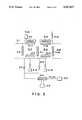
- FIG. 1is a schematic diagram showing the overall arrangement of the manufacturing apparatus according to a first embodiment of this invention
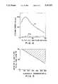
- FIG. 2is a graph showing the etching speeds of silicon (Si) and silicon oxide film (SiO 2 ) relative to temperature under microwave discharge plasma of a mixed gas of CF 4 and O 2 ;
- FIG. 3is a schematic diagram showing the overall arrangement of the manufacturing apparatus according to a second embodiment of this invention.
- FIG. 4is a graph showing the etching speeds of Si and SiO 2 under the microwave discharge plasma of a mixed gas of CF 4 and O 2 relative to the gas flow ratio O 2 /(CF 4 +O 2 );
- FIG. 5is a graph showing the etching condition region within which the ratio of substrate material to an oxide thereof becomes less than or equal to 5;
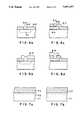
- FIGS. 6a to 6d and FIGS. 7a and 7bare cross sectional views showing some of the manufacturing steps performed by the apparatus of the first or second embodiments;
- FIG. 8is a schematic diagram showing the overall arrangement of the manufacturing apparatus according to a third embodiment of this invention.
- FIG. 9is a schematic diagram showing the overall arrangement of the manufacturing apparatus according to a fourth embodiment of this invention.
- the so-called chemical dry etchingis the most suitable method by which etching is performed with active species generated by the discharge plasma.
- the etching speed of a certain materialis generally very large when compared with that of an oxide of the material.
- the etching speed of siliconis about 30 times as large as that of silicon oxide. Therefore, with this method, the underlying layer at the thin surface oxide film may be etched considerably while the surface oxide layer is removed, and so this method is not suitable for practical use.
- the present inventorshave discovered the condition that the difference of the etching speeds between material and its oxide becomes considerably less even if such chemical dry etching is employed. Using this condition, an oxide film on the surface of an underlying layer can be removed properly.
- another filmcan be properly formed by using an apparatus for successively and sequentially depositing the film without degrading the property of a reduced pressure atmosphere so as to prevent the oxide film from re-growing and preventing surface grime.
- the present inventionhas been made on the basis of the above viewpoint.
- an apparatuswhereby an oxide film on the surface of an underlying silicon layer or underlying polysilicon layer is removed, and sequentially thereafter, polysilicon, silicon nitride, silicon oxide or the like, respectively containing therein impurities is, deposited.
- an oxide film on the surface of an underlying silicon layer or underlying polysilicon layeris removed, and sequentially thereafter, polysilicon, silicon nitride, silicon oxide or the like, respectively containing therein impurities is, deposited.
- FIG. 1shows the outline of the manufacturing apparatus of the first embodiment whose function and use will be given hereinbelow.
- an object substrate (silicon wafer) 11is inserted into a quartz tube 10 serving as a deposition chamber.
- the pressure within the quartz tube 10is reduced with an exhaust pump 12, to introduce gaseous He and gaseous SiH 4 from a He gas source 10A and SiH 4 gas source 10B, respectively.
- the wafer 11 within the tube 10is heated to around 600° C. with an external heater 13.
- a polysilicon filmis deposited on the wafer 11.
- the above-described reduced pressure CVD apparatusis coupled to a plasma discharge chamber in which gaseous CF 4 and gaseous O 2 from a CF 4 gas source 14A and O 2 gas source 14B, respectively, can be introduced via an introduction tube 17.
- gaseous CF 4 and gaseous O 2 from a CF 4 gas source 14A and O 2 gas source 14B, respectivelycan be introduced via an introduction tube 17.
- poweris supplied from a microwave power source 15 to the discharge chamber 14 to generate a plasma 16 of the mixed gases.
- reference numeral 21represents a flow regulator for regulating the flow ratio of O 2 to CF 4
- reference numeral 22represents a temperature regulator for regulating the temperature of an intermediate semiconductor device within the tube 10 under control of the heater 13.
- a silicon wafer with a partially exposed polysilicon layer or a partially exposed diffused layeris subjected to cleaning, washing and drying processes using ordinary chemicals and thereafter, it is inserted into the quartz tube 10.
- the pressure within the tube 10is reduced to about 10 -2 Torr using the exhaust pump 12, with the temperature of the wafer being raised u to 600° C.
- air within the discharge chamber 14is exhausted using the exhaust pump 12 to introduce therein a CF 4 gas and an O 2 gas to about 0.1 Torr under the condition of a flow ratio O 2 /(total gas flow) of about 50%.
- Microwave poweris applied from the microwave power source 15 to the discharge chamber 14 to generate a plasma. Active species F* generated by the plasma are introduced into the deposition chamber 10.
- the etching speeds of Si and SiO 2 under the active species F* relative to the temperature of the waferare shown in FIG. 2. Particularly, at the low temperature range (room temperature to 150° C.), a difference between the etching speeds of Si and SiO 2 is large, whereas at the temperature range over 400° C., the difference becomes small. Therefore, by applying the active species F* to the silicon wafer heated to 600° C., polysilicon diffused layer and oxide film thereof are etched for a time sufficient for etching the very thin silicon oxide film (50 to 100 ⁇ ) formed on the exposed polysilicon or the exposed diffused layer. In this case, these are etched to the same degree. Thus, the difference between the etching speeds of the polysilicon and diffused layer, and oxide film thereof can be substantially neglected. After etching the oxide film, the reduced pressure CVD method is performed using He gas and SiH 4 gas.
- polysilicon containing impuritiescan be deposited by using a gas containing impurities such as As, B, P and the like, or a silicon nitride film can be deposited by using ammonia.
- the apparatus of the second embodimenthas a reduced pressure CVD apparatus for deposition of a polysilicon or silicon nitride film, the surface processing chamber and film deposition chamber thereof being separately mounted.
- An object wafer substrate similar to the first embodimentis transported into a load chamber 3-1 which is then subjected to vacuum exhaustion. Thereafter, a gate valve 3-2 is opened to move the wafer 3-3 to a cleaning chamber 3-4 as shown in FIG. 3.
- the cleaning chamber 3-4is always maintained at reduced pressure by means of an air exhausting system 3-9.
- the temperature of the wafer 3-3 within the cleaning chamber 3-4is rapidly raised to 600° C. by means of an infrared heater 3-5 through a quartz glass window 3-17.
- a valve 3-7 between the cleaning chamber 3-4 and discharge chamber 3-6is opened, and a mixed gas of CF 4 and O 2 is introduced into the discharge chamber 3-6.
- the wafer 3-14 with polysilicon deposited thereon as aboveis transported into an unload chamber 3-16 via a gate valve 3-20. Thereafter, a gas introduction system 3-15 is caused to operate so that active species are introduced from the discharge chamber 3-6 to the deposition chamber 3-10 to therefore effectively remove polysilicon attached on the inner wall of the deposition chamber 3-10.
- reference numeral 3-21represents a flow regulator for regulating the flow ratio of O 2 to CF 4 (flow regulator in FIG. 8 is indicated at 8-21, and in FIG. 10 at 10-21), and reference numeral 3-22 represents a temperature regulator for regulating the temperature of an intermediate semiconductor device during etching (temperature regulator in FIG. 8 is indicated at 8-22, and in FIG. 10 at 10-22).
- the infrared heaters 3-5 and 3-12have been used for heating the wafers 3-3 and 3-14, respectively.
- other heating meanssuch as resistive wire heating means and induction heating means may also be used with the similar effects as above.
- etching in the cleaning chamber 3-4is carried out at a high temperature but cleaning may be carried out at lower temperatures, e.g., near room temperature if the ratio of O 2 to CF 4 of the gases to be introduced into the discharge chamber 3-6 is changed.
- FIG. 4illustrates a change in the etching speeds of polysilicon and silicon oxide film relative to the ratio of O 2 to (CF 4 +O 2 ) at room temperature.
- the difference between the etching speeds of Si and SiO 2becomes correspondingly small.
- a relatively large amount of O 2allows an oxide film on the silicon surface to be properly removed even at room temperature.
- a significant point in the surface processing described in the second embodimentis that the difference between the etching speeds of silicon and silicon oxide is made as small as possible.
- the present inventorshave thoroughly studied the etching of oxide films by using a mixed gas of a gaseous halogen compound and gaseous oxygen and have discovered that the gas flow ratio and temperature are important parameters. Taking into consideration the thickness of an oxide film and uniformity of etching, it can be judged that a practical value for the etching speed ratio of silicon to silicon oxide, is 5 or less. The region satisfying such a condition is indicated by oblique lines in FIG. 5. This region is given by the following formula:
- FIGS. 6a to 6dschematically show the processes of making polysilicon containing impurities come into contact with an underlying silicon diffused layer 6-1 (FIGS. 6a and 6b) and with an underlying polysilicon layer containing impurities 6-2 (FIGS. 6c and 6d).
- insulating layers 6-3such as a silicon oxide film are deposited on the underlying diffused layer 6-1 or on the underlying polysilicon layer 6-2.
- contact holes 6-4are formed above the insulating layers 6-3 for deposition of conductive polysilicon.
- thin natural oxide films 6-5may grow on the surface of the polysilicon layer 6-2 or silicon diffused layer 6-1.
- the oxide film 6-5is likely to grow more impurities are contained in the underlying silicon or polysilicon layers. Electrical connections are not ensured even if polysilicon is deposited on the oxide film 6-5 but in this case, by using the embodiment apparatus, the oxide film 6-5 can be removed properly. Immediately after this removal, upper polysilicon layers 6-6 can be deposited in the succeeding process to therefore allow satisfactory electrical connections (FIGS. 6b and 6d).
- FIGS. 7a and 7bOther applications of the above embodiments to a process of diffusing impurities into a silicon substrate are shown in FIGS. 7a and 7b.
- a silicon oxide 7-2 containing impurities such as As, P and Bis deposited on a silicon substrate 7-1. Thereafter, the impurities within the silicon oxide 7-2 are diffused into the silicon substrate 7-1 by means of heat treatment. If an oxide film 7-3 is present on the surface of the substrate 7-1 during the above processes, the diffusion at that portion is hindered (FIG. 7a).
- FIG. 7bshows a silicon oxide 7-2 containing impurities such as As, P and B.
- the above embodimentsare applicable to a silicon nitride film forming process, although this is not shown.
- a silicon oxide film, polysilicon and silicon nitride filmare deposited on a silicon substrate in this sequence.
- the silicon nitride filmis patterned in a predetermined shape to use it as a selective oxidation mask for forming a field region (field oxide film).
- the oxide film inevitably formed on the polysilicon at the process of depositing the silicon nitride on the polysiliconcan be removed so that abnormal oxidation during field oxidation can be avoided to therefore allow the formation of fine field regions.
- FIG. 8A third embodiment is shown in FIG. 8 wherein the above-described cleaning means is mounted on a sputtering apparatus having a load lock mechanism.
- an object silicon wafer substrate 8-2is transported from a load chamber- 8-3 into an airtight cleaning chamber 8-1.
- the wafer 8-2is heated by an external infrared heater 8-4 through a quartz glass window 8-5.
- the cleaning chamber 8-1is adapted to produce a vacuum by means of an air exhaust pump 8-6.
- the cleaning chamber 8-1is coupled to a discharge chamber 8-7 which has a structure similar to the discharge chamber 3-6 shown in FIG. 3.
- a deposition chamber 8-8 for performing ordinary sputteringis mounted next to the cleaning chamber 8-1.
- For the deposition chamber 8-8there are provided a sputtering target 8-9, a silicon wafer 8-10 facing the target, a d.c.
- Reference numeral 8-11represents a microwave power source
- 8-15, 8-18 and 8-19represent a gate valve.
- an object wafer 8-2is transported from the load chamber 8-3 into the cleaning chamber 8-1 as shown in FIG. 8.
- the inside of the load cleaning chamber 8-1 and discharge chamber 8-7is made a high vacuum state because of air exhaustion by an air exhaust system 8-6.
- a mixture gases of C1 2 , NF 3 and O 2is introduced into the discharge chamber 8-7 at about 0.1 Torr, and microwave power is supplied thereto from the microwave power source 8-13.
- dischargeoccurs within the discharge chamber 8-7 so that a number of active species are generated within the discharge chamber 8-7.
- the active speciesare introduced via an introduction system 8-14 into the cleaning chamber 8-1.
- the wafer 8-1 within the cleaning chamber 8-1has been heated with the infrared heater 8-4 to have a temperature of about 450° C. at the wafer surface.
- a silicon oxide film on the surface of the wafer 8-2can be easily etched out with the active species containing the radical of C1 or F.
- the reaction speeds of silicon and silicon oxide with the active speciesare substantially equal to each other at such a high temperature. Therefore, the underlying silicon is scarcely damaged while removing the thin silicon oxide film formed thereon.
- the gate valve 8-15is opened to transport the wafer 8-2 into the deposition chamber 8-8 to deposit an aluminum film for Al wiring on the silicon surface by means of sputtering. It was confirmed that the yield (provability) of electric connection between the underlying first layer and the A1 wiring second layer improved remarkably.
- the cleaning chamber 8-1 and deposition chamber 8-8have been provided separately in the apparatus shown in FIG. 8. However, they may be united into a single chamber to perform cleaning and deposition continuously and sequentially. Particularly in such a case, when a wafer is transported into a reaction chamber (single chamber), the reaction chamber is exhausted to a vacuum and simultaneously; therewith, the wafer is heated. Then, active species are introduced into the reaction chamber to remove an alumina layer 9-4 formed on an Al wiring first layer 9-1. Thereafter, the reaction chamber is again exhausted to create a high vacuum. Then, a gas such as Ar is introduced to deposit an Al wiring second layer through D.C. discharge sputtering.
- a fourth embodimentwill be described with reference to FIG. 9, which uses a cold wall type, reduced pressure CVD apparatus with a load lock mechanism.
- a cleaning chamber 10-1 of the apparatus shown in FIG. 9has the same structure as the cleaning chamber 8-1 shown in FIG. 8.
- a deposition chamber 10-2 for selective CVD of tungstenis mounted next the cleaning chamber 10-1.
- an air exhaust pump 10-3for the deposition chamber 10-2, there are provided an air exhaust pump 10-3, infrared heater 10-4, and quartz glass window 105 adapted so as to introduce WF 6 and H 2 .
- Reference numeral 10-6represents an air exhaust pump, 10-8 a microwave power source, 10-9 an infrared heater, 10-10 a quartz glass window, 10-11 a load chamber, 10-12 and 10-13 a wafer, and 10-15 to 10-17 a gate valve.
- a silicon wafer with or without contact holes formed therein(refer to hole 6-4 in FIG. 6a) is subjected to cleaning, washing and drying processes using ordinary chemicals and thereafter, transported into the cleaning chamber 10-1 into which active species generated within the discharge chamber 10-7 are introduced.
- a thin natural oxide film (refer to film 6-5 in FIG. 6a) formed on the silicon surface exposed to atmosphere at the bottom of contact holecan be easily etched out with the active species. Therefore, the silicon surface (refer to surface 6-1 in FIG. 6a) becomes clean without an oxide film.
- the silicon surfaceis covered with a silicon oxide film which has been soiled considerably mainly due to organic substances, typically vacuum pump oil.
- the active species generated from the mixed gas of CF 4 and O 2effectively etch out such organic substances.
- the active speciesslightly etch out the silicon oxide film so that the contaminated layer on the silicon surface can be completely removed and therefore expose an original, clean silicon oxide film.
- the inside of the cleaning chamber 10-1is exhausted by means of the air exhaustion pump 10-6, and the wafer 10-12 is transported into the deposition chamber 10-2 which has been previously maintained at a vacuum by means of the air exhaust pump 10-3 so that the surface of the wafer 10-13 can be maintained clean.
- a mixture gas of WF 6 and H 2is introduced into the deposition chamber 10-2 to selectively deposit W onto contact holes using the ordinary deposition conditions.
- the surfaces of the silicon and silicon oxide filmare maintained sufficiently clean for presenting their intrinsic performance, so that selective deposition of W sensitive to the surface condition can be realized.
- the discharge chambermay be mounted on an epitaxial growing deposition apparatus wherein dry cleaning the deposition surface is performed, prior to the deposition, at relatively low temperature of 500° to 600° C. using active species and thereafter, epitaxial growing is effected.
- the descriptionhas been directed to the case where an oxide film on the surface of silicon or aluminum is removed using CF 4 , NF 3 or Cl 2 .
- the present inventionis also applicable to other underlying materials such as high melting point metal, silicon compounds and the like, so long as the processes are performed for the purpose of improving contact between the underlying and overlaid layers by removing an oxide film or improving the overlaid film quality.
- other halogen compound gasessuch as CHF 3 , CFCl 3 and the like may be used.
- the apparatus shown in FIG. 1is used in this example.
- a substrateis inserted into the quartz tube 10 which is then subjected to pressure reduction. Thereafter, the silicon substrate is cleaned in the manner similar to the foregoing description. Then, an oxidizing gas such as O 2 or H 2 O is introduced into the quartz tube 10 to oxidize the silicon and grow a silicon oxide film.
- the grown silicon oxide filmcan be used as a gate oxide film having a good breakdown voltage.
Landscapes
- Engineering & Computer Science (AREA)
- Microelectronics & Electronic Packaging (AREA)
- Condensed Matter Physics & Semiconductors (AREA)
- General Physics & Mathematics (AREA)
- Manufacturing & Machinery (AREA)
- Computer Hardware Design (AREA)
- Physics & Mathematics (AREA)
- Power Engineering (AREA)
- Chemical & Material Sciences (AREA)
- Chemical Kinetics & Catalysis (AREA)
- General Chemical & Material Sciences (AREA)
- Inorganic Chemistry (AREA)
- Drying Of Semiconductors (AREA)
- Formation Of Insulating Films (AREA)
- Weting (AREA)
Abstract
Description
The present invention relates to a method of manufacturing semiconductor devices and an apparatus for practicing the method, wherein a silicon oxide film on the surface of an intermediate semiconductor device is etched out and then another film is deposited on the device.
In order to deposit polysilicon on the surface of, e.g., an intermediate semiconductor device at an intermediate stage of manufacturing processes by means of the reduced pressure chemical vapor deposition (CVD) method, it is necessary to chemically clean, prior to such deposition, the surface of a polysilicon layer on, or an impurity diffused layer in, the substrate. Thereafter, the substrate is washed or placed in atmosphere so that a very thin oxide film called a natural oxide film grows on the substrate surface. The oxide film grows further when the substrate is introduced into a reaction tube for deposition of a polysilicon film. Under such conditions, if a polysilicon film is deposited on the oxide film by the CVD method, a failure of the electric connection will occur. Such a problem is particularly serious where the underlying layer is a polysilicon layer. In order to avoid such failures, a so-called ion mixing method has been adopted whereby after the deposition of a polysilicon film on the substrate by the CVD method, ions are implanted to destruct the oxide film for achieving an electrical connection. This ion mixing method necessitates using an expensive ion implanting apparatus, and, in addition, the semiconductor device is subject to ion radiation damage.
There is a method where a silicon nitride film is deposited on a polysilicon film formed by the CVD method to use the former as a mask for field oxidation. Also in this method, film will grow on the polysilicon film. The presence of an oxide film between the polysilicon film and silicon nitride results in abnormal oxidation in many cases.
For the diffusion of impurities such as arsenic, boron, or the like into a silicon substrate, there is a method wherein a diffusion source such as polysilicon, silicon oxide or the like is deposited on the substrate to make impurities contained in the diffusion source diffuse into the substrate. In this method, if a silicon oxide film is present at the interface between the diffusion source and silicon substrate, then the silicon oxide film acts as a diffusion barrier that suppresses the diffusion of impurities into the silicon substrate.
If the silicon substrate is washed and thereafter exposed to the atmosphere prior to deposition of the diffusion source on a silicon substrate, a very thin oxide film will grow on the silicon substrate as described before. The presence of this oxide film makes it difficult to diffuse the impurities into the silicon substrate.
The selective CVD method is also known whereby W is selectively deposited on only silicon by using WF6 and H2. If silicon subjected to the selective CVD method has a thin oxide film thereon, W will not be deposited thereon. In addition, if the surface of silicon on which W is not deposited primarily is soiled, W will nevertheless be deposited but it will not be uniform in thickness. For these reasons, it is difficult to apply the selective CVD method.
As above, with the above-described techniques it is difficult in practice to form a new film on an intermediate semiconductor device without incuring an adverse effect from oxide films. Furthermore, an attempt remove such an oxide film will damage to the intermediate semiconductor device.
The present invention results from consideration of the above problems. It is an object of this invention to provide a method of manufacturing a semiconductor device and apparatus for use in practicing the method, capable of removing a silicon oxide film on an intermediate semiconductor device without damaging it, and then forming another film on the surface of the device.
The manufacturing method of this invention comprises the steps of: removing a surface oxide film on a surface material (silicon) of an intermediate semiconductor device, by using active species derived from a mixture of a gaseous halogen compound and gaseous oxygen, under the condition that the difference between the etching speeds of the surface material and the surface oxide film is made as small as possible by controlling the ratio of the flow of the gaseous oxygen to that of the mixed gas and the temperature of the intermediate semiconductor device; and forming another covering film on the surface of the surface material (silicon) with the surface oxide film removed therefrom.
The manufacturing apparatus of this invention comprises: first means for forming active species and second means for removing an oxide film and forming a covering film; the first means comprising a regulating means for regulating a flow ratio of gaseous oxygen gas to a gaseous halogen compound and a discharge means for forming active species based on the gases, with the second means comprising a casing (chamber) capable of introducing the active species therein for housing an object intermediate semiconductor device, a heating means for heating the intermediate semiconductor device to remove a surface oxide film on a surface material (silicon) of the intermediate semiconductor device by using the active species, a regulating means for regulating the temperature of the intermediate semiconductor device through control of the heating means, and a film forming means for forming a covering film on the surface material of the intermediate semiconductor device with the surface oxide film removed therefrom.
According to the manufacturing method of this invention, the flow ratio of the gaseous oxygen to a mixture gas of the gaseous oxygen and a gaseous halogen compound, and the temperature of an intermediate semiconductor device are both controlled. Therefore, it becomes possible to obtain the etching condition that a difference between the etching speeds of silicon and silicon oxide is made as small as possible. Under such an etching condition, an oxide film on the surface of an intermediate semiconductor device can be removed by using active species generated by the discharge in the mixed gas and without damaging the device. Another film is formed on the surface of the device. Since the surface of the device after removal of the oxide film is not exposed to the atmosphere, the other film can be reliably formed because the oxide film has been removed.
Removal of an oxide film is carried out properly where the etching speed ratio of silicon to silicon oxide, is less than or equal to 5.
The etching condition for the etching speed ratio less than or equal to 5, is obtained by satisfying the following formula:
Y≧-0.13 T+106.3
where Y is a percent flow ratio of gaseous oxygen to the mixed gas, and T is the temperature (° C.) of an intermediate semiconductor device.
According to the present invention, the flow ratio of oxygen gas to a mixture of gaseous oxygen and a gaseous halogen compound and the temperature of an intermediate semiconductor device, are both controlled. Therefore, the etching condition of the difference of the etching speeds between silicon and silicon oxide being as small as possible, is easily satisfied. Under such conditions, an oxide film on the surface of an intermediate semiconductor device can be removed without damaging the device, and another film can be formed.
FIG. 1 is a schematic diagram showing the overall arrangement of the manufacturing apparatus according to a first embodiment of this invention;
FIG. 2 is a graph showing the etching speeds of silicon (Si) and silicon oxide film (SiO2) relative to temperature under microwave discharge plasma of a mixed gas of CF4 and O2 ;
FIG. 3 is a schematic diagram showing the overall arrangement of the manufacturing apparatus according to a second embodiment of this invention;
FIG. 4 is a graph showing the etching speeds of Si and SiO2 under the microwave discharge plasma of a mixed gas of CF4 and O2 relative to the gas flow ratio O2 /(CF4 +O2);
FIG. 5 is a graph showing the etching condition region within which the ratio of substrate material to an oxide thereof becomes less than or equal to 5;
FIGS. 6a to 6d and FIGS. 7a and 7b are cross sectional views showing some of the manufacturing steps performed by the apparatus of the first or second embodiments;
FIG. 8 is a schematic diagram showing the overall arrangement of the manufacturing apparatus according to a third embodiment of this invention; and
FIG. 9 is a schematic diagram showing the overall arrangement of the manufacturing apparatus according to a fourth embodiment of this invention.
The background to how the present invention has been made will be described prior to the description of the embodiments.
For removing a surface oxide film on an underlying film without damaging it, and under a reduced pressure atmosphere, the so-called chemical dry etching is the most suitable method by which etching is performed with active species generated by the discharge plasma. However, in the usual chemical dry etching, the etching speed of a certain material is generally very large when compared with that of an oxide of the material. For example, the etching speed of silicon is about 30 times as large as that of silicon oxide. Therefore, with this method, the underlying layer at the thin surface oxide film may be etched considerably while the surface oxide layer is removed, and so this method is not suitable for practical use. The present inventors have discovered the condition that the difference of the etching speeds between material and its oxide becomes considerably less even if such chemical dry etching is employed. Using this condition, an oxide film on the surface of an underlying layer can be removed properly.
Furthermore, after removing the surface oxide film, another film can be properly formed by using an apparatus for successively and sequentially depositing the film without degrading the property of a reduced pressure atmosphere so as to prevent the oxide film from re-growing and preventing surface grime.
The present invention has been made on the basis of the above viewpoint.
Some of the preferred embodiments of this invention will now be described hereinbelow.
In this embodiment, an apparatus is provided whereby an oxide film on the surface of an underlying silicon layer or underlying polysilicon layer is removed, and sequentially thereafter, polysilicon, silicon nitride, silicon oxide or the like, respectively containing therein impurities is, deposited. Given further are examples of applications of the apparatus to the manufacture of semiconductor devices.
FIG. 1 shows the outline of the manufacturing apparatus of the first embodiment whose function and use will be given hereinbelow. Specifically, an object substrate (silicon wafer) 11 is inserted into aquartz tube 10 serving as a deposition chamber. Next, the pressure within thequartz tube 10 is reduced with anexhaust pump 12, to introduce gaseous He and gaseous SiH4 from a He gas source 10A and SiH4 gas source 10B, respectively. Then, the wafer 11 within thetube 10 is heated to around 600° C. with anexternal heater 13. Then, a polysilicon film is deposited on the wafer 11. The above-described reduced pressure CVD apparatus is coupled to a plasma discharge chamber in which gaseous CF4 and gaseous O2 from a CF4 gas source 14A and O2 gas source 14B, respectively, can be introduced via an introduction tube 17. With the gases introduced within the discharge chamber 14, power is supplied from a microwave power source 15 to the discharge chamber 14 to generate a plasma 16 of the mixed gases. In FIG. 1,reference numeral 21 represents a flow regulator for regulating the flow ratio of O2 to CF4, andreference numeral 22 represents a temperature regulator for regulating the temperature of an intermediate semiconductor device within thetube 10 under control of theheater 13.
Practicing the method of this invention by using the above apparatus will be described in detail.
First, a silicon wafer with a partially exposed polysilicon layer or a partially exposed diffused layer is subjected to cleaning, washing and drying processes using ordinary chemicals and thereafter, it is inserted into thequartz tube 10. The pressure within thetube 10 is reduced to about 10-2 Torr using theexhaust pump 12, with the temperature of the wafer being raised u to 600° C. Then, air within the discharge chamber 14 is exhausted using theexhaust pump 12 to introduce therein a CF4 gas and an O2 gas to about 0.1 Torr under the condition of a flow ratio O2 /(total gas flow) of about 50%. Microwave power is applied from the microwave power source 15 to the discharge chamber 14 to generate a plasma. Active species F* generated by the plasma are introduced into thedeposition chamber 10. The etching speeds of Si and SiO2 under the active species F* relative to the temperature of the wafer are shown in FIG. 2. Particularly, at the low temperature range (room temperature to 150° C.), a difference between the etching speeds of Si and SiO2 is large, whereas at the temperature range over 400° C., the difference becomes small. Therefore, by applying the active species F* to the silicon wafer heated to 600° C., polysilicon diffused layer and oxide film thereof are etched for a time sufficient for etching the very thin silicon oxide film (50 to 100 Å) formed on the exposed polysilicon or the exposed diffused layer. In this case, these are etched to the same degree. Thus, the difference between the etching speeds of the polysilicon and diffused layer, and oxide film thereof can be substantially neglected. After etching the oxide film, the reduced pressure CVD method is performed using He gas and SiH4 gas.
With the above apparatus, it becomes possible to deposit polysilicon on the surface of an underlying polysilicon layer or the like, after etching the surface oxide film without degrading the performance of reduced pressure atmosphere by sequentially employing the reduced pressure CVD method. Furthermore, polysilicon containing impurities can be deposited by using a gas containing impurities such as As, B, P and the like, or a silicon nitride film can be deposited by using ammonia.
Next, the second embodiment of the apparatus which is a modification of the first embodiment will be described with reference to FIG. 3. The apparatus of the second embodiment has a reduced pressure CVD apparatus for deposition of a polysilicon or silicon nitride film, the surface processing chamber and film deposition chamber thereof being separately mounted.
An object wafer substrate similar to the first embodiment is transported into a load chamber 3-1 which is then subjected to vacuum exhaustion. Thereafter, a gate valve 3-2 is opened to move the wafer 3-3 to a cleaning chamber 3-4 as shown in FIG. 3. The cleaning chamber 3-4 is always maintained at reduced pressure by means of an air exhausting system 3-9. The temperature of the wafer 3-3 within the cleaning chamber 3-4 is rapidly raised to 600° C. by means of an infrared heater 3-5 through a quartz glass window 3-17. Thereafter, a valve 3-7 between the cleaning chamber 3-4 and discharge chamber 3-6 is opened, and a mixed gas of CF4 and O2 is introduced into the discharge chamber 3-6. Upon application of microwave power from a microwave power source 3-8 to the discharge chamber 3-6, discharge is initiated within the discharge chamber 3-6. Active species generated by such discharge are introduced into the cleaning chamber 3-4 to remove any silicon oxide film on the surface of the wafer 3-3, in the manner similar to the first embodiment. Thereafter, the valve 3-7 is closed so that the cleaning chamber 3-4 is again subjected to air exhaustion and pressure reduction by means of the air exhausting system 3-9. Then, a gate valve 3-11 is opened to transport the wafer to the deposition chamber 3-10, the inside of which is exhausted by the air exhausting system 3-19. The wafer 3-14 within the deposition chamber 3-10 is heated to about 600° C. by means of an infrared heater 3-12 through a quartz glass window 3-18. SiH4 and He are introduced by a gas introduction system 3-13 so that polysilicon is deposited on the wafer 3-14 by means of the reduced pressure CVD method.
The wafer 3-14 with polysilicon deposited thereon as above is transported into an unload chamber 3-16 via a gate valve 3-20. Thereafter, a gas introduction system 3-15 is caused to operate so that active species are introduced from the discharge chamber 3-6 to the deposition chamber 3-10 to therefore effectively remove polysilicon attached on the inner wall of the deposition chamber 3-10.
In FIG. 3, reference numeral 3-21 represents a flow regulator for regulating the flow ratio of O2 to CF4 (flow regulator in FIG. 8 is indicated at 8-21, and in FIG. 10 at 10-21), and reference numeral 3-22 represents a temperature regulator for regulating the temperature of an intermediate semiconductor device during etching (temperature regulator in FIG. 8 is indicated at 8-22, and in FIG. 10 at 10-22).
In the second embodiment, the infrared heaters 3-5 and 3-12 have been used for heating the wafers 3-3 and 3-14, respectively. However, it is obvious that other heating means such as resistive wire heating means and induction heating means may also be used with the similar effects as above.
Furthermore, in the second embodiment, etching in the cleaning chamber 3-4 is carried out at a high temperature but cleaning may be carried out at lower temperatures, e.g., near room temperature if the ratio of O2 to CF4 of the gases to be introduced into the discharge chamber 3-6 is changed.
FIG. 4 illustrates a change in the etching speeds of polysilicon and silicon oxide film relative to the ratio of O2 to (CF4 +O2) at room temperature. As seen from FIG. 4, as the amount of O2 increases, the difference between the etching speeds of Si and SiO2 becomes correspondingly small. A relatively large amount of O2 allows an oxide film on the silicon surface to be properly removed even at room temperature.
A significant point in the surface processing described in the second embodiment is that the difference between the etching speeds of silicon and silicon oxide is made as small as possible. The present inventors have thoroughly studied the etching of oxide films by using a mixed gas of a gaseous halogen compound and gaseous oxygen and have discovered that the gas flow ratio and temperature are important parameters. Taking into consideration the thickness of an oxide film and uniformity of etching, it can be judged that a practical value for the etching speed ratio of silicon to silicon oxide, is 5 or less. The region satisfying such a condition is indicated by oblique lines in FIG. 5. This region is given by the following formula:
Y≧-0.13 T+106.3
where Y is a flow ratio in percent of the O2 gas to the total gas, and T (° C.) is the temperature of a substrate. As appreciated from the region indicated by oblique lines in FIG. 5, proper etching is possible even if the substrate temperature is lowered, under the condition that the amount of oxygen gas is increased. Therefore, proper etching at the room temperature may be carried out with a suitable flow ratio.
Next, examples of applications of the above embodiments to the manufacturing processes of practical FIGS. 6a to 6d, which schematically show the processes of making polysilicon containing impurities come into contact with an underlying silicon diffused layer 6-1 (FIGS. 6a and 6b) and with an underlying polysilicon layer containing impurities 6-2 (FIGS. 6c and 6d). In conducting such processes, insulating layers 6-3 such as a silicon oxide film are deposited on the underlying diffused layer 6-1 or on the underlying polysilicon layer 6-2. Thereafter, contact holes 6-4 are formed above the insulating layers 6-3 for deposition of conductive polysilicon. During these processes, thin natural oxide films 6-5 may grow on the surface of the polysilicon layer 6-2 or silicon diffused layer 6-1. The oxide film 6-5 is likely to grow more impurities are contained in the underlying silicon or polysilicon layers. Electrical connections are not ensured even if polysilicon is deposited on the oxide film 6-5 but in this case, by using the embodiment apparatus, the oxide film 6-5 can be removed properly. Immediately after this removal, upper polysilicon layers 6-6 can be deposited in the succeeding process to therefore allow satisfactory electrical connections (FIGS. 6b and 6d).
Other applications of the above embodiments to a process of diffusing impurities into a silicon substrate are shown in FIGS. 7a and 7b. As shown in FIG. 7a, a silicon oxide 7-2 containing impurities such as As, P and B is deposited on a silicon substrate 7-1. Thereafter, the impurities within the silicon oxide 7-2 are diffused into the silicon substrate 7-1 by means of heat treatment. If an oxide film 7-3 is present on the surface of the substrate 7-1 during the above processes, the diffusion at that portion is hindered (FIG. 7a). However, by using the above embodiments, it becomes possible to diffuse impurities into the silicon substrate 7-1 uniformly as shown in FIG. 7b.
The above embodiments are applicable to a silicon nitride film forming process, although this is not shown. In this process, a silicon oxide film, polysilicon and silicon nitride film are deposited on a silicon substrate in this sequence. Next, the silicon nitride film is patterned in a predetermined shape to use it as a selective oxidation mask for forming a field region (field oxide film). Upon application of the above embodiments to this process, the oxide film inevitably formed on the polysilicon at the process of depositing the silicon nitride on the polysilicon can be removed so that abnormal oxidation during field oxidation can be avoided to therefore allow the formation of fine field regions.
A third embodiment is shown in FIG. 8 wherein the above-described cleaning means is mounted on a sputtering apparatus having a load lock mechanism.
Referring to FIG. 8, an object silicon wafer substrate 8-2 is transported from a load chamber- 8-3 into an airtight cleaning chamber 8-1. The wafer 8-2 is heated by an external infrared heater 8-4 through a quartz glass window 8-5. The cleaning chamber 8-1 is adapted to produce a vacuum by means of an air exhaust pump 8-6. The cleaning chamber 8-1 is coupled to a discharge chamber 8-7 which has a structure similar to the discharge chamber 3-6 shown in FIG. 3. A deposition chamber 8-8 for performing ordinary sputtering is mounted next to the cleaning chamber 8-1. For the deposition chamber 8-8, there are provided a sputtering target 8-9, a silicon wafer 8-10 facing the target, a d.c. power source 8-11 for use in generating plasma from the front surface of the target by using gaseous Ar, and an air exhaust pump 8-12 to produce a vacuum of the chamber. Reference numeral 8-13 represents a microwave power source, and 8-15, 8-18 and 8-19 represent a gate valve.
Next, the operation of the apparatus will be described. First, an object wafer 8-2 is transported from the load chamber 8-3 into the cleaning chamber 8-1 as shown in FIG. 8. The inside of the load cleaning chamber 8-1 and discharge chamber 8-7 is made a high vacuum state because of air exhaustion by an air exhaust system 8-6. Thereafter, a mixture gases of C12, NF3 and O2 is introduced into the discharge chamber 8-7 at about 0.1 Torr, and microwave power is supplied thereto from the microwave power source 8-13. Then, discharge occurs within the discharge chamber 8-7 so that a number of active species are generated within the discharge chamber 8-7. The active species are introduced via an introduction system 8-14 into the cleaning chamber 8-1. The wafer 8-1 within the cleaning chamber 8-1 has been heated with the infrared heater 8-4 to have a temperature of about 450° C. at the wafer surface. At this high temperature, a silicon oxide film on the surface of the wafer 8-2 can be easily etched out with the active species containing the radical of C1 or F. The reaction speeds of silicon and silicon oxide with the active species are substantially equal to each other at such a high temperature. Therefore, the underlying silicon is scarcely damaged while removing the thin silicon oxide film formed thereon. After completion of the above cleaning processes, the gate valve 8-15 is opened to transport the wafer 8-2 into the deposition chamber 8-8 to deposit an aluminum film for Al wiring on the silicon surface by means of sputtering. It was confirmed that the yield (provability) of electric connection between the underlying first layer and the A1 wiring second layer improved remarkably.
The cleaning chamber 8-1 and deposition chamber 8-8 have been provided separately in the apparatus shown in FIG. 8. However, they may be united into a single chamber to perform cleaning and deposition continuously and sequentially. Particularly in such a case, when a wafer is transported into a reaction chamber (single chamber), the reaction chamber is exhausted to a vacuum and simultaneously; therewith, the wafer is heated. Then, active species are introduced into the reaction chamber to remove an alumina layer 9-4 formed on an Al wiring first layer 9-1. Thereafter, the reaction chamber is again exhausted to create a high vacuum. Then, a gas such as Ar is introduced to deposit an Al wiring second layer through D.C. discharge sputtering.
A fourth embodiment will be described with reference to FIG. 9, which uses a cold wall type, reduced pressure CVD apparatus with a load lock mechanism. A cleaning chamber 10-1 of the apparatus shown in FIG. 9 has the same structure as the cleaning chamber 8-1 shown in FIG. 8. A deposition chamber 10-2 for selective CVD of tungsten is mounted next the cleaning chamber 10-1. For the deposition chamber 10-2, there are provided an air exhaust pump 10-3, infrared heater 10-4, and quartz glass window 105 adapted so as to introduce WF6 and H2. Reference numeral 10-6 represents an air exhaust pump, 10-8 a microwave power source, 10-9 an infrared heater, 10-10 a quartz glass window, 10-11 a load chamber, 10-12 and 10-13 a wafer, and 10-15 to 10-17 a gate valve.
Next, processing a wafer by the apparatus will be described. First, a silicon wafer with or without contact holes formed therein (refer to hole 6-4 in FIG. 6a) is subjected to cleaning, washing and drying processes using ordinary chemicals and thereafter, transported into the cleaning chamber 10-1 into which active species generated within the discharge chamber 10-7 are introduced.
A thin natural oxide film (refer to film 6-5 in FIG. 6a) formed on the silicon surface exposed to atmosphere at the bottom of contact hole can be easily etched out with the active species. Therefore, the silicon surface (refer to surface 6-1 in FIG. 6a) becomes clean without an oxide film. Alternatively, in the case of a silicon wafer without contact holes, the silicon surface is covered with a silicon oxide film which has been soiled considerably mainly due to organic substances, typically vacuum pump oil. However, the active species generated from the mixed gas of CF4 and O2 effectively etch out such organic substances. In addition, the active species slightly etch out the silicon oxide film so that the contaminated layer on the silicon surface can be completely removed and therefore expose an original, clean silicon oxide film.
Under such conditions, the inside of the cleaning chamber 10-1 is exhausted by means of the air exhaustion pump 10-6, and the wafer 10-12 is transported into the deposition chamber 10-2 which has been previously maintained at a vacuum by means of the air exhaust pump 10-3 so that the surface of the wafer 10-13 can be maintained clean. A mixture gas of WF6 and H2 is introduced into the deposition chamber 10-2 to selectively deposit W onto contact holes using the ordinary deposition conditions.
During the above processes, the surfaces of the silicon and silicon oxide film are maintained sufficiently clean for presenting their intrinsic performance, so that selective deposition of W sensitive to the surface condition can be realized.
Similar to the modification of the apparatus shown in FIG. 8, the above processes may be carried out in time sequence by using a single reaction chamber instead of two chambers 10-1 and 10-2.
Furthermore, the discharge chamber may be mounted on an epitaxial growing deposition apparatus wherein dry cleaning the deposition surface is performed, prior to the deposition, at relatively low temperature of 500° to 600° C. using active species and thereafter, epitaxial growing is effected.
For the processes by the apparatus shown in FIGS. 3, 8 and 9, the description has been directed to the case where an oxide film on the surface of silicon or aluminum is removed using CF4, NF3 or Cl2. However, the present invention is also applicable to other underlying materials such as high melting point metal, silicon compounds and the like, so long as the processes are performed for the purpose of improving contact between the underlying and overlaid layers by removing an oxide film or improving the overlaid film quality. In addition, other halogen compound gases such as CHF3, CFCl3 and the like may be used.
Even if a silicon substrate has been cleaned to expose the clean silicon surface, the silicon surface is again subjected to contamination if it is exposed to atmosphere, through adsorption of hydrocarbon mist, sulfuric acid mist, hydrochloric acid mist or oil mist, in the atmosphere. Therefore, after such adsorption of impurities, a satisfactory oxide film such as a thin oxide film of a gate oxide film may sometimes be impossible to grow on the impurities. To avoid such adsorption of impurities, an example of an oxidation apparatus with the above-described cleaning method applied thereto will be described.
The apparatus shown in FIG. 1 is used in this example. A substrate is inserted into thequartz tube 10 which is then subjected to pressure reduction. Thereafter, the silicon substrate is cleaned in the manner similar to the foregoing description. Then, an oxidizing gas such as O2 or H2 O is introduced into thequartz tube 10 to oxidize the silicon and grow a silicon oxide film. The grown silicon oxide film can be used as a gate oxide film having a good breakdown voltage.
Claims (12)
1. An apparatus for forming a covering film on the silicon surface of an intermediate semiconductor device, comprising:
first means for forming an active species, and
second means for removing an oxide film and forming a covering film;
said first means being a flow ratio regulating means for regulating a flow ratio of gaseous oxygen to a gaseous halogen compound, and discharge means for forming an active species from said gases;
said second means including a casing for housing an intermediate semiconductor device formed of silicon and for introducing said active species, a heating means for heating said intermediate semiconductor device to remove a silicon oxide film formed on said silicon surface of the intermediate semiconductor device by using said active species, temperature regulating means for regulating the temperature of said intermediate semiconductor device, and film forming means for forming a covering film on said silicon surface of said intermediate semiconductor device after said silicon oxide film has been removed therefrom;
said flow ratio regulating means and said temperature regulating means cooperatively regulating said flow ratio and said temperature, respectively, the ratio of the etching speeds of said silicon and said silicon oxide film being 5 or less.
2. An apparatus according to claim 1, further comprising means for reducing the pressure within said casing.
3. An apparatus according to claim 1, wherein said film forming means comprises means for introducing a gas into said casing for the deposition of material on said silicon surface of said intermediate semiconductor by the CVD method.
4. An apparatus according to claim 1, wherein said casing is divided into a first chamber for removing said silicon oxide film and a second chamber for performing said covering film forming.
5. An apparatus according to claim 4, wherein said second chamber comprises said film forming means and said film forming means is a means for performing sputtering.
6. An apparatus according to claim 1, wherein said casing comprises one chamber for removing said silicon oxide film and for performing said film forming, sequentially.
7. An apparatus according to claim 1, wherein said flow ratio regulating means and said temperature regulating means regulate said flow ratio and said temperature, respectively, so as to satisfy the following formula:
Y≧-0.13T+106.3
where Y is a percent flow ratio of said oxygen gas to said mixed gas, and T is the temperature (° C.) of said intermediate semiconductor device.
8. An apparatus according to claim 7, further comprising means for reducing the pressure within said casing.
9. An apparatus according to claim 7, wherein said film forming means comprises means for introducing a gas into said casing for the deposition of material on said silicon surface of said intermediate semiconductor by the CVD method.
10. An apparatus according to claim 7, wherein said casing is divided into a first chamber for removing said silicon oxide film and a second chamber for performing said film forming.
11. An apparatus according to claim 10, wherein said second chamber comprises said film forming means and said film forming means is a means for performing sputtering.
12. An apparatus according to claim 7, wherein said casing comprises one chamber both for removing said silicon oxide film and for performing said film forming, sequentially.
Priority Applications (1)
| Application Number | Priority Date | Filing Date | Title |
|---|---|---|---|
| US07/759,903US5225036A (en) | 1988-03-28 | 1991-09-13 | Method of manufacturing semiconductor device |
Applications Claiming Priority (2)
| Application Number | Priority Date | Filing Date | Title |
|---|---|---|---|
| JP63-73628 | 1988-03-28 | ||
| JP63073628AJP2768685B2 (en) | 1988-03-28 | 1988-03-28 | Semiconductor device manufacturing method and device |
Related Child Applications (1)
| Application Number | Title | Priority Date | Filing Date |
|---|---|---|---|
| US07/759,903DivisionUS5225036A (en) | 1988-03-28 | 1991-09-13 | Method of manufacturing semiconductor device |
Publications (1)
| Publication Number | Publication Date |
|---|---|
| US5067437Atrue US5067437A (en) | 1991-11-26 |
Family
ID=13523770
Family Applications (1)
| Application Number | Title | Priority Date | Filing Date |
|---|---|---|---|
| US07/329,847Expired - LifetimeUS5067437A (en) | 1988-03-28 | 1989-03-28 | Apparatus for coating of silicon semiconductor surface |
Country Status (4)
| Country | Link |
|---|---|
| US (1) | US5067437A (en) |
| EP (1) | EP0335313A3 (en) |
| JP (1) | JP2768685B2 (en) |
| KR (1) | KR920006261B1 (en) |
Cited By (287)
| Publication number | Priority date | Publication date | Assignee | Title |
|---|---|---|---|---|
| US5425810A (en)* | 1994-05-11 | 1995-06-20 | Internation Business Machines Corporation | Removable gas injectors for use in chemical vapor deposition of aluminium oxide |
| US5707451A (en)* | 1994-02-03 | 1998-01-13 | Applied Materials, Inc. | Method and apparatus for cleaning a throttle valve |
| US5877064A (en)* | 1997-07-15 | 1999-03-02 | Taiwan Semiconductor Manufacturing Co.Ltd | Method for marking a wafer |
| US6348420B1 (en) | 1999-12-23 | 2002-02-19 | Asm America, Inc. | Situ dielectric stacks |
| US6352594B2 (en)* | 1997-08-11 | 2002-03-05 | Torrex | Method and apparatus for improved chemical vapor deposition processes using tunable temperature controlled gas injectors |
| US6352593B1 (en)* | 1997-08-11 | 2002-03-05 | Torrex Equipment Corp. | Mini-batch process chamber |
| US6432830B1 (en)* | 1998-05-15 | 2002-08-13 | Applied Materials, Inc. | Semiconductor fabrication process |
| US20030049372A1 (en)* | 1997-08-11 | 2003-03-13 | Cook Robert C. | High rate deposition at low pressures in a small batch reactor |
| US20030134038A1 (en)* | 1997-08-11 | 2003-07-17 | Paranjpe Ajit P. | Method and apparatus for layer by layer deposition of thin films |
| US6749687B1 (en) | 1998-01-09 | 2004-06-15 | Asm America, Inc. | In situ growth of oxide and silicon layers |
| US20100093185A1 (en)* | 2006-09-29 | 2010-04-15 | Tokyo Electron Limited | Method for forming silicon oxide film, plasma processing apparatus and storage medium |
| TWI421913B (en)* | 2008-08-26 | 2014-01-01 | He Jian Technology Suzhou Co Ltd | Method of depositing polycrystalline silicon in a furnace |
| US9099481B2 (en) | 2013-03-15 | 2015-08-04 | Semiconductor Components Industries, Llc | Methods of laser marking semiconductor substrates |
| US11001925B2 (en) | 2016-12-19 | 2021-05-11 | Asm Ip Holding B.V. | Substrate processing apparatus |
| US11004977B2 (en) | 2017-07-19 | 2021-05-11 | Asm Ip Holding B.V. | Method for depositing a group IV semiconductor and related semiconductor device structures |
| US11018002B2 (en) | 2017-07-19 | 2021-05-25 | Asm Ip Holding B.V. | Method for selectively depositing a Group IV semiconductor and related semiconductor device structures |
| US11015245B2 (en) | 2014-03-19 | 2021-05-25 | Asm Ip Holding B.V. | Gas-phase reactor and system having exhaust plenum and components thereof |
| US11022879B2 (en) | 2017-11-24 | 2021-06-01 | Asm Ip Holding B.V. | Method of forming an enhanced unexposed photoresist layer |
| US11031242B2 (en) | 2018-11-07 | 2021-06-08 | Asm Ip Holding B.V. | Methods for depositing a boron doped silicon germanium film |
| USD922229S1 (en) | 2019-06-05 | 2021-06-15 | Asm Ip Holding B.V. | Device for controlling a temperature of a gas supply unit |
| US11049751B2 (en) | 2018-09-14 | 2021-06-29 | Asm Ip Holding B.V. | Cassette supply system to store and handle cassettes and processing apparatus equipped therewith |
| US11056344B2 (en) | 2017-08-30 | 2021-07-06 | Asm Ip Holding B.V. | Layer forming method |
| US11053591B2 (en) | 2018-08-06 | 2021-07-06 | Asm Ip Holding B.V. | Multi-port gas injection system and reactor system including same |
| US11069510B2 (en) | 2017-08-30 | 2021-07-20 | Asm Ip Holding B.V. | Substrate processing apparatus |
| US11081345B2 (en) | 2018-02-06 | 2021-08-03 | Asm Ip Holding B.V. | Method of post-deposition treatment for silicon oxide film |
| US11088002B2 (en) | 2018-03-29 | 2021-08-10 | Asm Ip Holding B.V. | Substrate rack and a substrate processing system and method |
| US11087997B2 (en) | 2018-10-31 | 2021-08-10 | Asm Ip Holding B.V. | Substrate processing apparatus for processing substrates |
| US11094546B2 (en) | 2017-10-05 | 2021-08-17 | Asm Ip Holding B.V. | Method for selectively depositing a metallic film on a substrate |
| US11094582B2 (en) | 2016-07-08 | 2021-08-17 | Asm Ip Holding B.V. | Selective deposition method to form air gaps |
| US11101370B2 (en) | 2016-05-02 | 2021-08-24 | Asm Ip Holding B.V. | Method of forming a germanium oxynitride film |
| US11107676B2 (en) | 2016-07-28 | 2021-08-31 | Asm Ip Holding B.V. | Method and apparatus for filling a gap |
| US11114283B2 (en) | 2018-03-16 | 2021-09-07 | Asm Ip Holding B.V. | Reactor, system including the reactor, and methods of manufacturing and using same |
| US11114294B2 (en) | 2019-03-08 | 2021-09-07 | Asm Ip Holding B.V. | Structure including SiOC layer and method of forming same |
| USD930782S1 (en) | 2019-08-22 | 2021-09-14 | Asm Ip Holding B.V. | Gas distributor |
| US11127617B2 (en) | 2017-11-27 | 2021-09-21 | Asm Ip Holding B.V. | Storage device for storing wafer cassettes for use with a batch furnace |
| US11127589B2 (en) | 2019-02-01 | 2021-09-21 | Asm Ip Holding B.V. | Method of topology-selective film formation of silicon oxide |
| USD931978S1 (en) | 2019-06-27 | 2021-09-28 | Asm Ip Holding B.V. | Showerhead vacuum transport |
| US11139191B2 (en) | 2017-08-09 | 2021-10-05 | Asm Ip Holding B.V. | Storage apparatus for storing cassettes for substrates and processing apparatus equipped therewith |
| US11139308B2 (en) | 2015-12-29 | 2021-10-05 | Asm Ip Holding B.V. | Atomic layer deposition of III-V compounds to form V-NAND devices |
| US11158513B2 (en) | 2018-12-13 | 2021-10-26 | Asm Ip Holding B.V. | Methods for forming a rhenium-containing film on a substrate by a cyclical deposition process and related semiconductor device structures |
| US11164955B2 (en) | 2017-07-18 | 2021-11-02 | Asm Ip Holding B.V. | Methods for forming a semiconductor device structure and related semiconductor device structures |
| US11168395B2 (en) | 2018-06-29 | 2021-11-09 | Asm Ip Holding B.V. | Temperature-controlled flange and reactor system including same |
| US11171025B2 (en) | 2019-01-22 | 2021-11-09 | Asm Ip Holding B.V. | Substrate processing device |
| USD935572S1 (en) | 2019-05-24 | 2021-11-09 | Asm Ip Holding B.V. | Gas channel plate |
| US11205585B2 (en) | 2016-07-28 | 2021-12-21 | Asm Ip Holding B.V. | Substrate processing apparatus and method of operating the same |
| US11217444B2 (en) | 2018-11-30 | 2022-01-04 | Asm Ip Holding B.V. | Method for forming an ultraviolet radiation responsive metal oxide-containing film |
| USD940837S1 (en) | 2019-08-22 | 2022-01-11 | Asm Ip Holding B.V. | Electrode |
| US11222772B2 (en) | 2016-12-14 | 2022-01-11 | Asm Ip Holding B.V. | Substrate processing apparatus |
| US11227782B2 (en) | 2019-07-31 | 2022-01-18 | Asm Ip Holding B.V. | Vertical batch furnace assembly |
| US11227789B2 (en) | 2019-02-20 | 2022-01-18 | Asm Ip Holding B.V. | Method and apparatus for filling a recess formed within a substrate surface |
| US11230766B2 (en) | 2018-03-29 | 2022-01-25 | Asm Ip Holding B.V. | Substrate processing apparatus and method |
| US11233133B2 (en) | 2015-10-21 | 2022-01-25 | Asm Ip Holding B.V. | NbMC layers |
| US11232963B2 (en) | 2018-10-03 | 2022-01-25 | Asm Ip Holding B.V. | Substrate processing apparatus and method |
| US11242598B2 (en) | 2015-06-26 | 2022-02-08 | Asm Ip Holding B.V. | Structures including metal carbide material, devices including the structures, and methods of forming same |
| US11244825B2 (en) | 2018-11-16 | 2022-02-08 | Asm Ip Holding B.V. | Methods for depositing a transition metal chalcogenide film on a substrate by a cyclical deposition process |
| US11251040B2 (en) | 2019-02-20 | 2022-02-15 | Asm Ip Holding B.V. | Cyclical deposition method including treatment step and apparatus for same |
| US11251068B2 (en) | 2018-10-19 | 2022-02-15 | Asm Ip Holding B.V. | Substrate processing apparatus and substrate processing method |
| US11251035B2 (en) | 2016-12-22 | 2022-02-15 | Asm Ip Holding B.V. | Method of forming a structure on a substrate |
| USD944946S1 (en) | 2019-06-14 | 2022-03-01 | Asm Ip Holding B.V. | Shower plate |
| US11270899B2 (en) | 2018-06-04 | 2022-03-08 | Asm Ip Holding B.V. | Wafer handling chamber with moisture reduction |
| US11274369B2 (en) | 2018-09-11 | 2022-03-15 | Asm Ip Holding B.V. | Thin film deposition method |
| US11282698B2 (en) | 2019-07-19 | 2022-03-22 | Asm Ip Holding B.V. | Method of forming topology-controlled amorphous carbon polymer film |
| US11286558B2 (en) | 2019-08-23 | 2022-03-29 | Asm Ip Holding B.V. | Methods for depositing a molybdenum nitride film on a surface of a substrate by a cyclical deposition process and related semiconductor device structures including a molybdenum nitride film |
| US11286562B2 (en) | 2018-06-08 | 2022-03-29 | Asm Ip Holding B.V. | Gas-phase chemical reactor and method of using same |
| US11289326B2 (en) | 2019-05-07 | 2022-03-29 | Asm Ip Holding B.V. | Method for reforming amorphous carbon polymer film |
| US11295980B2 (en) | 2017-08-30 | 2022-04-05 | Asm Ip Holding B.V. | Methods for depositing a molybdenum metal film over a dielectric surface of a substrate by a cyclical deposition process and related semiconductor device structures |
| US11296189B2 (en) | 2018-06-21 | 2022-04-05 | Asm Ip Holding B.V. | Method for depositing a phosphorus doped silicon arsenide film and related semiconductor device structures |
| USD947913S1 (en) | 2019-05-17 | 2022-04-05 | Asm Ip Holding B.V. | Susceptor shaft |
| USD948463S1 (en) | 2018-10-24 | 2022-04-12 | Asm Ip Holding B.V. | Susceptor for semiconductor substrate supporting apparatus |
| US11306395B2 (en) | 2017-06-28 | 2022-04-19 | Asm Ip Holding B.V. | Methods for depositing a transition metal nitride film on a substrate by atomic layer deposition and related deposition apparatus |
| USD949319S1 (en) | 2019-08-22 | 2022-04-19 | Asm Ip Holding B.V. | Exhaust duct |
| US11315794B2 (en) | 2019-10-21 | 2022-04-26 | Asm Ip Holding B.V. | Apparatus and methods for selectively etching films |
| US11339476B2 (en) | 2019-10-08 | 2022-05-24 | Asm Ip Holding B.V. | Substrate processing device having connection plates, substrate processing method |
| US11342216B2 (en) | 2019-02-20 | 2022-05-24 | Asm Ip Holding B.V. | Cyclical deposition method and apparatus for filling a recess formed within a substrate surface |
| US11345999B2 (en) | 2019-06-06 | 2022-05-31 | Asm Ip Holding B.V. | Method of using a gas-phase reactor system including analyzing exhausted gas |
| US11355338B2 (en) | 2019-05-10 | 2022-06-07 | Asm Ip Holding B.V. | Method of depositing material onto a surface and structure formed according to the method |
| US11361990B2 (en) | 2018-05-28 | 2022-06-14 | Asm Ip Holding B.V. | Substrate processing method and device manufactured by using the same |
| US11374112B2 (en) | 2017-07-19 | 2022-06-28 | Asm Ip Holding B.V. | Method for depositing a group IV semiconductor and related semiconductor device structures |
| US11378337B2 (en) | 2019-03-28 | 2022-07-05 | Asm Ip Holding B.V. | Door opener and substrate processing apparatus provided therewith |
| US11387120B2 (en) | 2017-09-28 | 2022-07-12 | Asm Ip Holding B.V. | Chemical dispensing apparatus and methods for dispensing a chemical to a reaction chamber |
| US11387106B2 (en) | 2018-02-14 | 2022-07-12 | Asm Ip Holding B.V. | Method for depositing a ruthenium-containing film on a substrate by a cyclical deposition process |
| US11390945B2 (en) | 2019-07-03 | 2022-07-19 | Asm Ip Holding B.V. | Temperature control assembly for substrate processing apparatus and method of using same |
| US11393690B2 (en) | 2018-01-19 | 2022-07-19 | Asm Ip Holding B.V. | Deposition method |
| US11390950B2 (en) | 2017-01-10 | 2022-07-19 | Asm Ip Holding B.V. | Reactor system and method to reduce residue buildup during a film deposition process |
| US11390946B2 (en) | 2019-01-17 | 2022-07-19 | Asm Ip Holding B.V. | Methods of forming a transition metal containing film on a substrate by a cyclical deposition process |
| US11396702B2 (en) | 2016-11-15 | 2022-07-26 | Asm Ip Holding B.V. | Gas supply unit and substrate processing apparatus including the gas supply unit |
| US11398382B2 (en) | 2018-03-27 | 2022-07-26 | Asm Ip Holding B.V. | Method of forming an electrode on a substrate and a semiconductor device structure including an electrode |
| US11401605B2 (en) | 2019-11-26 | 2022-08-02 | Asm Ip Holding B.V. | Substrate processing apparatus |
| US11411088B2 (en) | 2018-11-16 | 2022-08-09 | Asm Ip Holding B.V. | Methods for forming a metal silicate film on a substrate in a reaction chamber and related semiconductor device structures |
| US11410851B2 (en) | 2017-02-15 | 2022-08-09 | Asm Ip Holding B.V. | Methods for forming a metallic film on a substrate by cyclical deposition and related semiconductor device structures |
| US11414760B2 (en) | 2018-10-08 | 2022-08-16 | Asm Ip Holding B.V. | Substrate support unit, thin film deposition apparatus including the same, and substrate processing apparatus including the same |
| US11417545B2 (en) | 2017-08-08 | 2022-08-16 | Asm Ip Holding B.V. | Radiation shield |
| US11424119B2 (en) | 2019-03-08 | 2022-08-23 | Asm Ip Holding B.V. | Method for selective deposition of silicon nitride layer and structure including selectively-deposited silicon nitride layer |
| US11430640B2 (en) | 2019-07-30 | 2022-08-30 | Asm Ip Holding B.V. | Substrate processing apparatus |
| US11430674B2 (en) | 2018-08-22 | 2022-08-30 | Asm Ip Holding B.V. | Sensor array, apparatus for dispensing a vapor phase reactant to a reaction chamber and related methods |
| US11437241B2 (en) | 2020-04-08 | 2022-09-06 | Asm Ip Holding B.V. | Apparatus and methods for selectively etching silicon oxide films |
| US11443926B2 (en) | 2019-07-30 | 2022-09-13 | Asm Ip Holding B.V. | Substrate processing apparatus |
| US11447864B2 (en) | 2019-04-19 | 2022-09-20 | Asm Ip Holding B.V. | Layer forming method and apparatus |
| US11447861B2 (en) | 2016-12-15 | 2022-09-20 | Asm Ip Holding B.V. | Sequential infiltration synthesis apparatus and a method of forming a patterned structure |
| USD965044S1 (en) | 2019-08-19 | 2022-09-27 | Asm Ip Holding B.V. | Susceptor shaft |
| US11453943B2 (en) | 2016-05-25 | 2022-09-27 | Asm Ip Holding B.V. | Method for forming carbon-containing silicon/metal oxide or nitride film by ALD using silicon precursor and hydrocarbon precursor |
| USD965524S1 (en) | 2019-08-19 | 2022-10-04 | Asm Ip Holding B.V. | Susceptor support |
| US11469098B2 (en) | 2018-05-08 | 2022-10-11 | Asm Ip Holding B.V. | Methods for depositing an oxide film on a substrate by a cyclical deposition process and related device structures |
| US11473195B2 (en) | 2018-03-01 | 2022-10-18 | Asm Ip Holding B.V. | Semiconductor processing apparatus and a method for processing a substrate |
| US11476109B2 (en) | 2019-06-11 | 2022-10-18 | Asm Ip Holding B.V. | Method of forming an electronic structure using reforming gas, system for performing the method, and structure formed using the method |
| US11482412B2 (en) | 2018-01-19 | 2022-10-25 | Asm Ip Holding B.V. | Method for depositing a gap-fill layer by plasma-assisted deposition |
| US11482418B2 (en) | 2018-02-20 | 2022-10-25 | Asm Ip Holding B.V. | Substrate processing method and apparatus |
| US11482533B2 (en) | 2019-02-20 | 2022-10-25 | Asm Ip Holding B.V. | Apparatus and methods for plug fill deposition in 3-D NAND applications |
| US11488854B2 (en) | 2020-03-11 | 2022-11-01 | Asm Ip Holding B.V. | Substrate handling device with adjustable joints |
| US11488819B2 (en) | 2018-12-04 | 2022-11-01 | Asm Ip Holding B.V. | Method of cleaning substrate processing apparatus |
| US11492703B2 (en) | 2018-06-27 | 2022-11-08 | Asm Ip Holding B.V. | Cyclic deposition methods for forming metal-containing material and films and structures including the metal-containing material |
| US11495459B2 (en) | 2019-09-04 | 2022-11-08 | Asm Ip Holding B.V. | Methods for selective deposition using a sacrificial capping layer |
| US11499222B2 (en) | 2018-06-27 | 2022-11-15 | Asm Ip Holding B.V. | Cyclic deposition methods for forming metal-containing material and films and structures including the metal-containing material |
| US11501973B2 (en) | 2018-01-16 | 2022-11-15 | Asm Ip Holding B.V. | Method for depositing a material film on a substrate within a reaction chamber by a cyclical deposition process and related device structures |
| US11501956B2 (en) | 2012-10-12 | 2022-11-15 | Asm Ip Holding B.V. | Semiconductor reaction chamber showerhead |
| US11499226B2 (en) | 2018-11-02 | 2022-11-15 | Asm Ip Holding B.V. | Substrate supporting unit and a substrate processing device including the same |
| US11501968B2 (en) | 2019-11-15 | 2022-11-15 | Asm Ip Holding B.V. | Method for providing a semiconductor device with silicon filled gaps |
| US11515187B2 (en) | 2020-05-01 | 2022-11-29 | Asm Ip Holding B.V. | Fast FOUP swapping with a FOUP handler |
| US11515188B2 (en) | 2019-05-16 | 2022-11-29 | Asm Ip Holding B.V. | Wafer boat handling device, vertical batch furnace and method |
| US11521851B2 (en) | 2020-02-03 | 2022-12-06 | Asm Ip Holding B.V. | Method of forming structures including a vanadium or indium layer |
| US11527403B2 (en) | 2019-12-19 | 2022-12-13 | Asm Ip Holding B.V. | Methods for filling a gap feature on a substrate surface and related semiconductor structures |
| US11527400B2 (en) | 2019-08-23 | 2022-12-13 | Asm Ip Holding B.V. | Method for depositing silicon oxide film having improved quality by peald using bis(diethylamino)silane |
| US11530876B2 (en) | 2020-04-24 | 2022-12-20 | Asm Ip Holding B.V. | Vertical batch furnace assembly comprising a cooling gas supply |
| US11532757B2 (en) | 2016-10-27 | 2022-12-20 | Asm Ip Holding B.V. | Deposition of charge trapping layers |
| US11530483B2 (en) | 2018-06-21 | 2022-12-20 | Asm Ip Holding B.V. | Substrate processing system |
| US11551912B2 (en) | 2020-01-20 | 2023-01-10 | Asm Ip Holding B.V. | Method of forming thin film and method of modifying surface of thin film |
| US11551925B2 (en) | 2019-04-01 | 2023-01-10 | Asm Ip Holding B.V. | Method for manufacturing a semiconductor device |
| US11557474B2 (en) | 2019-07-29 | 2023-01-17 | Asm Ip Holding B.V. | Methods for selective deposition utilizing n-type dopants and/or alternative dopants to achieve high dopant incorporation |
| USD975665S1 (en) | 2019-05-17 | 2023-01-17 | Asm Ip Holding B.V. | Susceptor shaft |
| US11562901B2 (en) | 2019-09-25 | 2023-01-24 | Asm Ip Holding B.V. | Substrate processing method |
| US11572620B2 (en) | 2018-11-06 | 2023-02-07 | Asm Ip Holding B.V. | Methods for selectively depositing an amorphous silicon film on a substrate |
| US11581186B2 (en) | 2016-12-15 | 2023-02-14 | Asm Ip Holding B.V. | Sequential infiltration synthesis apparatus |
| US11587815B2 (en) | 2019-07-31 | 2023-02-21 | Asm Ip Holding B.V. | Vertical batch furnace assembly |
| US11587821B2 (en) | 2017-08-08 | 2023-02-21 | Asm Ip Holding B.V. | Substrate lift mechanism and reactor including same |
| US11587814B2 (en) | 2019-07-31 | 2023-02-21 | Asm Ip Holding B.V. | Vertical batch furnace assembly |
| US11594600B2 (en) | 2019-11-05 | 2023-02-28 | Asm Ip Holding B.V. | Structures with doped semiconductor layers and methods and systems for forming same |
| US11594450B2 (en) | 2019-08-22 | 2023-02-28 | Asm Ip Holding B.V. | Method for forming a structure with a hole |
| USD979506S1 (en) | 2019-08-22 | 2023-02-28 | Asm Ip Holding B.V. | Insulator |
| USD980814S1 (en) | 2021-05-11 | 2023-03-14 | Asm Ip Holding B.V. | Gas distributor for substrate processing apparatus |
| USD980813S1 (en) | 2021-05-11 | 2023-03-14 | Asm Ip Holding B.V. | Gas flow control plate for substrate processing apparatus |
| US11605528B2 (en) | 2019-07-09 | 2023-03-14 | Asm Ip Holding B.V. | Plasma device using coaxial waveguide, and substrate treatment method |
| US11610775B2 (en) | 2016-07-28 | 2023-03-21 | Asm Ip Holding B.V. | Method and apparatus for filling a gap |
| US11610774B2 (en) | 2019-10-02 | 2023-03-21 | Asm Ip Holding B.V. | Methods for forming a topographically selective silicon oxide film by a cyclical plasma-enhanced deposition process |
| USD981973S1 (en) | 2021-05-11 | 2023-03-28 | Asm Ip Holding B.V. | Reactor wall for substrate processing apparatus |
| US11615970B2 (en) | 2019-07-17 | 2023-03-28 | Asm Ip Holding B.V. | Radical assist ignition plasma system and method |
| US11626308B2 (en) | 2020-05-13 | 2023-04-11 | Asm Ip Holding B.V. | Laser alignment fixture for a reactor system |
| US11626316B2 (en) | 2019-11-20 | 2023-04-11 | Asm Ip Holding B.V. | Method of depositing carbon-containing material on a surface of a substrate, structure formed using the method, and system for forming the structure |
| US11629406B2 (en) | 2018-03-09 | 2023-04-18 | Asm Ip Holding B.V. | Semiconductor processing apparatus comprising one or more pyrometers for measuring a temperature of a substrate during transfer of the substrate |
| US11629407B2 (en) | 2019-02-22 | 2023-04-18 | Asm Ip Holding B.V. | Substrate processing apparatus and method for processing substrates |
| US11637011B2 (en) | 2019-10-16 | 2023-04-25 | Asm Ip Holding B.V. | Method of topology-selective film formation of silicon oxide |
| US11637014B2 (en) | 2019-10-17 | 2023-04-25 | Asm Ip Holding B.V. | Methods for selective deposition of doped semiconductor material |
| US11639548B2 (en) | 2019-08-21 | 2023-05-02 | Asm Ip Holding B.V. | Film-forming material mixed-gas forming device and film forming device |
| US11639811B2 (en) | 2017-11-27 | 2023-05-02 | Asm Ip Holding B.V. | Apparatus including a clean mini environment |
| US11643724B2 (en) | 2019-07-18 | 2023-05-09 | Asm Ip Holding B.V. | Method of forming structures using a neutral beam |
| US11644758B2 (en) | 2020-07-17 | 2023-05-09 | Asm Ip Holding B.V. | Structures and methods for use in photolithography |
| US11646205B2 (en) | 2019-10-29 | 2023-05-09 | Asm Ip Holding B.V. | Methods of selectively forming n-type doped material on a surface, systems for selectively forming n-type doped material, and structures formed using same |
| US11646184B2 (en) | 2019-11-29 | 2023-05-09 | Asm Ip Holding B.V. | Substrate processing apparatus |
| US11646197B2 (en) | 2018-07-03 | 2023-05-09 | Asm Ip Holding B.V. | Method for depositing silicon-free carbon-containing film as gap-fill layer by pulse plasma-assisted deposition |
| US11646204B2 (en) | 2020-06-24 | 2023-05-09 | Asm Ip Holding B.V. | Method for forming a layer provided with silicon |
| US11649546B2 (en) | 2016-07-08 | 2023-05-16 | Asm Ip Holding B.V. | Organic reactants for atomic layer deposition |
| US11658029B2 (en) | 2018-12-14 | 2023-05-23 | Asm Ip Holding B.V. | Method of forming a device structure using selective deposition of gallium nitride and system for same |
| US11658035B2 (en) | 2020-06-30 | 2023-05-23 | Asm Ip Holding B.V. | Substrate processing method |
| US11658030B2 (en) | 2017-03-29 | 2023-05-23 | Asm Ip Holding B.V. | Method for forming doped metal oxide films on a substrate by cyclical deposition and related semiconductor device structures |
| US11664245B2 (en) | 2019-07-16 | 2023-05-30 | Asm Ip Holding B.V. | Substrate processing device |
| US11664267B2 (en) | 2019-07-10 | 2023-05-30 | Asm Ip Holding B.V. | Substrate support assembly and substrate processing device including the same |
| US11664199B2 (en) | 2018-10-19 | 2023-05-30 | Asm Ip Holding B.V. | Substrate processing apparatus and substrate processing method |
| US11676812B2 (en) | 2016-02-19 | 2023-06-13 | Asm Ip Holding B.V. | Method for forming silicon nitride film selectively on top/bottom portions |
| US11674220B2 (en) | 2020-07-20 | 2023-06-13 | Asm Ip Holding B.V. | Method for depositing molybdenum layers using an underlayer |
| US11680839B2 (en) | 2019-08-05 | 2023-06-20 | Asm Ip Holding B.V. | Liquid level sensor for a chemical source vessel |
| USD990441S1 (en) | 2021-09-07 | 2023-06-27 | Asm Ip Holding B.V. | Gas flow control plate |
| US11685991B2 (en) | 2018-02-14 | 2023-06-27 | Asm Ip Holding B.V. | Method for depositing a ruthenium-containing film on a substrate by a cyclical deposition process |
| US11688603B2 (en) | 2019-07-17 | 2023-06-27 | Asm Ip Holding B.V. | Methods of forming silicon germanium structures |
| USD990534S1 (en) | 2020-09-11 | 2023-06-27 | Asm Ip Holding B.V. | Weighted lift pin |
| US11705333B2 (en) | 2020-05-21 | 2023-07-18 | Asm Ip Holding B.V. | Structures including multiple carbon layers and methods of forming and using same |
| US11718913B2 (en) | 2018-06-04 | 2023-08-08 | Asm Ip Holding B.V. | Gas distribution system and reactor system including same |
| US11725277B2 (en) | 2011-07-20 | 2023-08-15 | Asm Ip Holding B.V. | Pressure transmitter for a semiconductor processing environment |
| US11725280B2 (en) | 2020-08-26 | 2023-08-15 | Asm Ip Holding B.V. | Method for forming metal silicon oxide and metal silicon oxynitride layers |
| US11735422B2 (en) | 2019-10-10 | 2023-08-22 | Asm Ip Holding B.V. | Method of forming a photoresist underlayer and structure including same |
| US11742189B2 (en) | 2015-03-12 | 2023-08-29 | Asm Ip Holding B.V. | Multi-zone reactor, system including the reactor, and method of using the same |
| US11742198B2 (en) | 2019-03-08 | 2023-08-29 | Asm Ip Holding B.V. | Structure including SiOCN layer and method of forming same |
| US11767589B2 (en) | 2020-05-29 | 2023-09-26 | Asm Ip Holding B.V. | Substrate processing device |
| US11769682B2 (en) | 2017-08-09 | 2023-09-26 | Asm Ip Holding B.V. | Storage apparatus for storing cassettes for substrates and processing apparatus equipped therewith |
| US11776846B2 (en) | 2020-02-07 | 2023-10-03 | Asm Ip Holding B.V. | Methods for depositing gap filling fluids and related systems and devices |
| US11781221B2 (en) | 2019-05-07 | 2023-10-10 | Asm Ip Holding B.V. | Chemical source vessel with dip tube |
| US11781243B2 (en) | 2020-02-17 | 2023-10-10 | Asm Ip Holding B.V. | Method for depositing low temperature phosphorous-doped silicon |
| US11795545B2 (en) | 2014-10-07 | 2023-10-24 | Asm Ip Holding B.V. | Multiple temperature range susceptor, assembly, reactor and system including the susceptor, and methods of using the same |
| US11804388B2 (en) | 2018-09-11 | 2023-10-31 | Asm Ip Holding B.V. | Substrate processing apparatus and method |
| US11802338B2 (en) | 2017-07-26 | 2023-10-31 | Asm Ip Holding B.V. | Chemical treatment, deposition and/or infiltration apparatus and method for using the same |
| US11804364B2 (en) | 2020-05-19 | 2023-10-31 | Asm Ip Holding B.V. | Substrate processing apparatus |
| US11810788B2 (en) | 2016-11-01 | 2023-11-07 | Asm Ip Holding B.V. | Methods for forming a transition metal niobium nitride film on a substrate by atomic layer deposition and related semiconductor device structures |
| US11814747B2 (en) | 2019-04-24 | 2023-11-14 | Asm Ip Holding B.V. | Gas-phase reactor system-with a reaction chamber, a solid precursor source vessel, a gas distribution system, and a flange assembly |
| US11823876B2 (en) | 2019-09-05 | 2023-11-21 | Asm Ip Holding B.V. | Substrate processing apparatus |
| US11821078B2 (en) | 2020-04-15 | 2023-11-21 | Asm Ip Holding B.V. | Method for forming precoat film and method for forming silicon-containing film |
| US11823866B2 (en) | 2020-04-02 | 2023-11-21 | Asm Ip Holding B.V. | Thin film forming method |
| US11828707B2 (en) | 2020-02-04 | 2023-11-28 | Asm Ip Holding B.V. | Method and apparatus for transmittance measurements of large articles |
| US11827981B2 (en) | 2020-10-14 | 2023-11-28 | Asm Ip Holding B.V. | Method of depositing material on stepped structure |
| US11830730B2 (en) | 2017-08-29 | 2023-11-28 | Asm Ip Holding B.V. | Layer forming method and apparatus |
| US11830738B2 (en) | 2020-04-03 | 2023-11-28 | Asm Ip Holding B.V. | Method for forming barrier layer and method for manufacturing semiconductor device |
| US11840761B2 (en) | 2019-12-04 | 2023-12-12 | Asm Ip Holding B.V. | Substrate processing apparatus |
| US11848200B2 (en) | 2017-05-08 | 2023-12-19 | Asm Ip Holding B.V. | Methods for selectively forming a silicon nitride film on a substrate and related semiconductor device structures |
| US11873557B2 (en) | 2020-10-22 | 2024-01-16 | Asm Ip Holding B.V. | Method of depositing vanadium metal |
| US11876356B2 (en) | 2020-03-11 | 2024-01-16 | Asm Ip Holding B.V. | Lockout tagout assembly and system and method of using same |
| US11885013B2 (en) | 2019-12-17 | 2024-01-30 | Asm Ip Holding B.V. | Method of forming vanadium nitride layer and structure including the vanadium nitride layer |
| US11887857B2 (en) | 2020-04-24 | 2024-01-30 | Asm Ip Holding B.V. | Methods and systems for depositing a layer comprising vanadium, nitrogen, and a further element |
| USD1012873S1 (en) | 2020-09-24 | 2024-01-30 | Asm Ip Holding B.V. | Electrode for semiconductor processing apparatus |
| US11885020B2 (en) | 2020-12-22 | 2024-01-30 | Asm Ip Holding B.V. | Transition metal deposition method |
| US11885023B2 (en) | 2018-10-01 | 2024-01-30 | Asm Ip Holding B.V. | Substrate retaining apparatus, system including the apparatus, and method of using same |
| US11891696B2 (en) | 2020-11-30 | 2024-02-06 | Asm Ip Holding B.V. | Injector configured for arrangement within a reaction chamber of a substrate processing apparatus |
| US11901179B2 (en) | 2020-10-28 | 2024-02-13 | Asm Ip Holding B.V. | Method and device for depositing silicon onto substrates |
| US11898243B2 (en) | 2020-04-24 | 2024-02-13 | Asm Ip Holding B.V. | Method of forming vanadium nitride-containing layer |
| US11915929B2 (en) | 2019-11-26 | 2024-02-27 | Asm Ip Holding B.V. | Methods for selectively forming a target film on a substrate comprising a first dielectric surface and a second metallic surface |
| US11923181B2 (en) | 2019-11-29 | 2024-03-05 | Asm Ip Holding B.V. | Substrate processing apparatus for minimizing the effect of a filling gas during substrate processing |
| US11923190B2 (en) | 2018-07-03 | 2024-03-05 | Asm Ip Holding B.V. | Method for depositing silicon-free carbon-containing film as gap-fill layer by pulse plasma-assisted deposition |
| US11929251B2 (en) | 2019-12-02 | 2024-03-12 | Asm Ip Holding B.V. | Substrate processing apparatus having electrostatic chuck and substrate processing method |
| US11939673B2 (en) | 2018-02-23 | 2024-03-26 | Asm Ip Holding B.V. | Apparatus for detecting or monitoring for a chemical precursor in a high temperature environment |
| US11946137B2 (en) | 2020-12-16 | 2024-04-02 | Asm Ip Holding B.V. | Runout and wobble measurement fixtures |
| US11959168B2 (en) | 2020-04-29 | 2024-04-16 | Asm Ip Holding B.V. | Solid source precursor vessel |
| US11961741B2 (en) | 2020-03-12 | 2024-04-16 | Asm Ip Holding B.V. | Method for fabricating layer structure having target topological profile |
| USD1023959S1 (en) | 2021-05-11 | 2024-04-23 | Asm Ip Holding B.V. | Electrode for substrate processing apparatus |
| US11967488B2 (en) | 2013-02-01 | 2024-04-23 | Asm Ip Holding B.V. | Method for treatment of deposition reactor |
| US11976359B2 (en) | 2020-01-06 | 2024-05-07 | Asm Ip Holding B.V. | Gas supply assembly, components thereof, and reactor system including same |
| US11986868B2 (en) | 2020-02-28 | 2024-05-21 | Asm Ip Holding B.V. | System dedicated for parts cleaning |
| US11987881B2 (en) | 2020-05-22 | 2024-05-21 | Asm Ip Holding B.V. | Apparatus for depositing thin films using hydrogen peroxide |
| US11996289B2 (en) | 2020-04-16 | 2024-05-28 | Asm Ip Holding B.V. | Methods of forming structures including silicon germanium and silicon layers, devices formed using the methods, and systems for performing the methods |
| US11996309B2 (en) | 2019-05-16 | 2024-05-28 | Asm Ip Holding B.V. | Wafer boat handling device, vertical batch furnace and method |
| US11996292B2 (en) | 2019-10-25 | 2024-05-28 | Asm Ip Holding B.V. | Methods for filling a gap feature on a substrate surface and related semiconductor structures |
| US11993847B2 (en) | 2020-01-08 | 2024-05-28 | Asm Ip Holding B.V. | Injector |
| US12009241B2 (en) | 2019-10-14 | 2024-06-11 | Asm Ip Holding B.V. | Vertical batch furnace assembly with detector to detect cassette |
| US12009224B2 (en) | 2020-09-29 | 2024-06-11 | Asm Ip Holding B.V. | Apparatus and method for etching metal nitrides |
| US12006572B2 (en) | 2019-10-08 | 2024-06-11 | Asm Ip Holding B.V. | Reactor system including a gas distribution assembly for use with activated species and method of using same |
| US12020934B2 (en) | 2020-07-08 | 2024-06-25 | Asm Ip Holding B.V. | Substrate processing method |
| US12027365B2 (en) | 2020-11-24 | 2024-07-02 | Asm Ip Holding B.V. | Methods for filling a gap and related systems and devices |
| US12025484B2 (en) | 2018-05-08 | 2024-07-02 | Asm Ip Holding B.V. | Thin film forming method |
| US12033885B2 (en) | 2020-01-06 | 2024-07-09 | Asm Ip Holding B.V. | Channeled lift pin |
| US12040177B2 (en) | 2020-08-18 | 2024-07-16 | Asm Ip Holding B.V. | Methods for forming a laminate film by cyclical plasma-enhanced deposition processes |
| US12040199B2 (en) | 2018-11-28 | 2024-07-16 | Asm Ip Holding B.V. | Substrate processing apparatus for processing substrates |
| US12040184B2 (en) | 2017-10-30 | 2024-07-16 | Asm Ip Holding B.V. | Methods for forming a semiconductor structure and related semiconductor structures |
| US12040200B2 (en) | 2017-06-20 | 2024-07-16 | Asm Ip Holding B.V. | Semiconductor processing apparatus and methods for calibrating a semiconductor processing apparatus |
| US12051602B2 (en) | 2020-05-04 | 2024-07-30 | Asm Ip Holding B.V. | Substrate processing system for processing substrates with an electronics module located behind a door in a front wall of the substrate processing system |
| US12051567B2 (en) | 2020-10-07 | 2024-07-30 | Asm Ip Holding B.V. | Gas supply unit and substrate processing apparatus including gas supply unit |
| US12057314B2 (en) | 2020-05-15 | 2024-08-06 | Asm Ip Holding B.V. | Methods for silicon germanium uniformity control using multiple precursors |
| US12074022B2 (en) | 2020-08-27 | 2024-08-27 | Asm Ip Holding B.V. | Method and system for forming patterned structures using multiple patterning process |
| US12087586B2 (en) | 2020-04-15 | 2024-09-10 | Asm Ip Holding B.V. | Method of forming chromium nitride layer and structure including the chromium nitride layer |
| US12107005B2 (en) | 2020-10-06 | 2024-10-01 | Asm Ip Holding B.V. | Deposition method and an apparatus for depositing a silicon-containing material |
| US12106944B2 (en) | 2020-06-02 | 2024-10-01 | Asm Ip Holding B.V. | Rotating substrate support |
| US12112940B2 (en) | 2019-07-19 | 2024-10-08 | Asm Ip Holding B.V. | Method of forming topology-controlled amorphous carbon polymer film |
| US12125700B2 (en) | 2020-01-16 | 2024-10-22 | Asm Ip Holding B.V. | Method of forming high aspect ratio features |
| US12131885B2 (en) | 2020-12-22 | 2024-10-29 | Asm Ip Holding B.V. | Plasma treatment device having matching box |
| US12129545B2 (en) | 2020-12-22 | 2024-10-29 | Asm Ip Holding B.V. | Precursor capsule, a vessel and a method |
| US12148609B2 (en) | 2020-09-16 | 2024-11-19 | Asm Ip Holding B.V. | Silicon oxide deposition method |
| US12154824B2 (en) | 2020-08-14 | 2024-11-26 | Asm Ip Holding B.V. | Substrate processing method |
| US12159788B2 (en) | 2020-12-14 | 2024-12-03 | Asm Ip Holding B.V. | Method of forming structures for threshold voltage control |
| US12169361B2 (en) | 2019-07-30 | 2024-12-17 | Asm Ip Holding B.V. | Substrate processing apparatus and method |
| US12173404B2 (en) | 2020-03-17 | 2024-12-24 | Asm Ip Holding B.V. | Method of depositing epitaxial material, structure formed using the method, and system for performing the method |
| US12173402B2 (en) | 2018-02-15 | 2024-12-24 | Asm Ip Holding B.V. | Method of forming a transition metal containing film on a substrate by a cyclical deposition process, a method for supplying a transition metal halide compound to a reaction chamber, and related vapor deposition apparatus |
| US12195852B2 (en) | 2020-11-23 | 2025-01-14 | Asm Ip Holding B.V. | Substrate processing apparatus with an injector |
| US12203166B2 (en) | 2020-05-07 | 2025-01-21 | Asm Ip Holding B.V. | Apparatus and methods for performing an in-situ etch of reaction chambers with fluorine-based radicals |
| US12211742B2 (en) | 2020-09-10 | 2025-01-28 | Asm Ip Holding B.V. | Methods for depositing gap filling fluid |
| US12209308B2 (en) | 2020-11-12 | 2025-01-28 | Asm Ip Holding B.V. | Reactor and related methods |
| US12217954B2 (en) | 2020-08-25 | 2025-02-04 | Asm Ip Holding B.V. | Method of cleaning a surface |
| US12218000B2 (en) | 2020-09-25 | 2025-02-04 | Asm Ip Holding B.V. | Semiconductor processing method |
| US12217946B2 (en) | 2020-10-15 | 2025-02-04 | Asm Ip Holding B.V. | Method of manufacturing semiconductor device, and substrate treatment apparatus using ether-CAT |
| US12218269B2 (en) | 2020-02-13 | 2025-02-04 | Asm Ip Holding B.V. | Substrate processing apparatus including light receiving device and calibration method of light receiving device |
| USD1060598S1 (en) | 2021-12-03 | 2025-02-04 | Asm Ip Holding B.V. | Split showerhead cover |
| US12221357B2 (en) | 2020-04-24 | 2025-02-11 | Asm Ip Holding B.V. | Methods and apparatus for stabilizing vanadium compounds |
| US12230531B2 (en) | 2018-04-09 | 2025-02-18 | Asm Ip Holding B.V. | Substrate supporting apparatus, substrate processing apparatus including the same, and substrate processing method |
| US12240760B2 (en) | 2016-03-18 | 2025-03-04 | Asm Ip Holding B.V. | Aligned carbon nanotubes |
| US12243742B2 (en) | 2020-04-21 | 2025-03-04 | Asm Ip Holding B.V. | Method for processing a substrate |
| US12243747B2 (en) | 2020-04-24 | 2025-03-04 | Asm Ip Holding B.V. | Methods of forming structures including vanadium boride and vanadium phosphide layers |
| US12241158B2 (en) | 2020-07-20 | 2025-03-04 | Asm Ip Holding B.V. | Method for forming structures including transition metal layers |
| US12243757B2 (en) | 2020-05-21 | 2025-03-04 | Asm Ip Holding B.V. | Flange and apparatus for processing substrates |
| US12247286B2 (en) | 2019-08-09 | 2025-03-11 | Asm Ip Holding B.V. | Heater assembly including cooling apparatus and method of using same |
| US12252785B2 (en) | 2019-06-10 | 2025-03-18 | Asm Ip Holding B.V. | Method for cleaning quartz epitaxial chambers |
| US12255053B2 (en) | 2020-12-10 | 2025-03-18 | Asm Ip Holding B.V. | Methods and systems for depositing a layer |
| US12266524B2 (en) | 2020-06-16 | 2025-04-01 | Asm Ip Holding B.V. | Method for depositing boron containing silicon germanium layers |
| US12272527B2 (en) | 2018-05-09 | 2025-04-08 | Asm Ip Holding B.V. | Apparatus for use with hydrogen radicals and method of using same |
| US12278129B2 (en) | 2020-03-04 | 2025-04-15 | Asm Ip Holding B.V. | Alignment fixture for a reactor system |
| US12276023B2 (en) | 2017-08-04 | 2025-04-15 | Asm Ip Holding B.V. | Showerhead assembly for distributing a gas within a reaction chamber |
| US12288710B2 (en) | 2020-12-18 | 2025-04-29 | Asm Ip Holding B.V. | Wafer processing apparatus with a rotatable table |
| US12322591B2 (en) | 2020-07-27 | 2025-06-03 | Asm Ip Holding B.V. | Thin film deposition process |
| US12378665B2 (en) | 2018-10-26 | 2025-08-05 | Asm Ip Holding B.V. | High temperature coatings for a preclean and etch apparatus and related methods |
| US12406846B2 (en) | 2020-05-26 | 2025-09-02 | Asm Ip Holding B.V. | Method for depositing boron and gallium containing silicon germanium layers |
| US12410515B2 (en) | 2020-01-29 | 2025-09-09 | Asm Ip Holding B.V. | Contaminant trap system for a reactor system |
| US12428726B2 (en) | 2019-10-08 | 2025-09-30 | Asm Ip Holding B.V. | Gas injection system and reactor system including same |
| US12431334B2 (en) | 2020-02-13 | 2025-09-30 | Asm Ip Holding B.V. | Gas distribution assembly |
| US12431354B2 (en) | 2020-07-01 | 2025-09-30 | Asm Ip Holding B.V. | Silicon nitride and silicon oxide deposition methods using fluorine inhibitor |
| US12444599B2 (en) | 2021-12-08 | 2025-10-14 | Asm Ip Holding B.V. | Method for forming an ultraviolet radiation responsive metal oxide-containing film |
Families Citing this family (6)
| Publication number | Priority date | Publication date | Assignee | Title |
|---|---|---|---|---|
| JPH01298181A (en)* | 1988-05-25 | 1989-12-01 | Hitachi Ltd | Dry etching method |
| JP2744934B2 (en)* | 1989-07-25 | 1998-04-28 | 東京エレクトロン株式会社 | Vertical processing equipment |
| DE69024719T2 (en)* | 1989-08-14 | 1996-10-02 | Applied Materials Inc | Gas distribution system and method of using this system |
| KR100472175B1 (en)* | 1997-08-25 | 2005-06-28 | 삼성전자주식회사 | Manufacturing method of semiconductor device using molybdenum or molybdenum alloy |
| NL1009767C2 (en)* | 1998-07-29 | 2000-02-04 | Asm Int | Method and device for etching a substrate. |
| CN103545162B (en)* | 2012-07-09 | 2016-06-08 | 北京北方微电子基地设备工艺研究中心有限责任公司 | Plasma reaction device and quartz window heating means |
Citations (16)
| Publication number | Priority date | Publication date | Assignee | Title |
|---|---|---|---|---|
| JPS5362982A (en)* | 1976-11-17 | 1978-06-05 | Toshiba Corp | Plasma cvd apparatus |
| US4138306A (en)* | 1976-08-31 | 1979-02-06 | Tokyo Shibaura Electric Co., Ltd. | Apparatus for the treatment of semiconductors |
| EP0052227A1 (en)* | 1980-11-19 | 1982-05-26 | International Business Machines Corporation | Method for forming a self-aligned contact and a plasma especially applicable in performing said method |
| US4484979A (en)* | 1984-04-16 | 1984-11-27 | At&T Bell Laboratories | Two-step anisotropic etching process for patterning a layer without penetrating through an underlying thinner layer |
| EP0157052A1 (en)* | 1984-03-16 | 1985-10-09 | Genus, Inc. | Low resistivity tungsten silicon composite film |
| JPS60249328A (en)* | 1984-05-25 | 1985-12-10 | Kokusai Electric Co Ltd | Dry etching/chemical vapor generation equipment for semiconductor wafers |
| US4581100A (en)* | 1984-10-29 | 1986-04-08 | International Business Machines Corporation | Mixed excitation plasma etching system |
| JPS61179868A (en)* | 1985-02-05 | 1986-08-12 | Canon Inc | Deposited film formation method |
| US4605479A (en)* | 1985-06-24 | 1986-08-12 | Rca Corporation | In-situ cleaned ohmic contacts |
| JPS6220331A (en)* | 1985-07-18 | 1987-01-28 | Fujitsu Ltd | Selectively growing method for alumina film |
| US4693777A (en)* | 1984-11-30 | 1987-09-15 | Kabushiki Kaisha Toshiba | Apparatus for producing semiconductor devices |
| JPS62221116A (en)* | 1986-03-24 | 1987-09-29 | Hitachi Micro Comput Eng Ltd | Plasma treating apparatus |
| JPS62221163A (en)* | 1986-03-24 | 1987-09-29 | Toppan Printing Co Ltd | Formation of thin film transistor |
| EP0242207A2 (en)* | 1986-04-15 | 1987-10-21 | Canon Kabushiki Kaisha | Process for forming deposited film |
| US4825808A (en)* | 1986-12-19 | 1989-05-02 | Anelva Corporation | Substrate processing apparatus |
| US4866346A (en)* | 1987-06-22 | 1989-09-12 | Applied Science & Technology, Inc. | Microwave plasma generator |
Family Cites Families (3)
| Publication number | Priority date | Publication date | Assignee | Title |
|---|---|---|---|---|
| JPS57114235A (en)* | 1981-01-08 | 1982-07-16 | Toshiba Corp | Cleaning of semiconductor substrate |
| JPS62274082A (en)* | 1986-05-20 | 1987-11-28 | Toshiba Corp | Dry etching method |
| JPS6353929A (en)* | 1986-08-22 | 1988-03-08 | Fuji Xerox Co Ltd | Manufacture of semiconductor device |
- 1988
- 1988-03-28JPJP63073628Apatent/JP2768685B2/ennot_activeExpired - Fee Related
- 1989
- 1989-03-28USUS07/329,847patent/US5067437A/ennot_activeExpired - Lifetime
- 1989-03-28KRKR1019890003912Apatent/KR920006261B1/ennot_activeExpired
- 1989-03-28EPEP19890105425patent/EP0335313A3/ennot_activeCeased
Patent Citations (16)
| Publication number | Priority date | Publication date | Assignee | Title |
|---|---|---|---|---|
| US4138306A (en)* | 1976-08-31 | 1979-02-06 | Tokyo Shibaura Electric Co., Ltd. | Apparatus for the treatment of semiconductors |
| JPS5362982A (en)* | 1976-11-17 | 1978-06-05 | Toshiba Corp | Plasma cvd apparatus |
| EP0052227A1 (en)* | 1980-11-19 | 1982-05-26 | International Business Machines Corporation | Method for forming a self-aligned contact and a plasma especially applicable in performing said method |
| EP0157052A1 (en)* | 1984-03-16 | 1985-10-09 | Genus, Inc. | Low resistivity tungsten silicon composite film |
| US4484979A (en)* | 1984-04-16 | 1984-11-27 | At&T Bell Laboratories | Two-step anisotropic etching process for patterning a layer without penetrating through an underlying thinner layer |
| JPS60249328A (en)* | 1984-05-25 | 1985-12-10 | Kokusai Electric Co Ltd | Dry etching/chemical vapor generation equipment for semiconductor wafers |
| US4581100A (en)* | 1984-10-29 | 1986-04-08 | International Business Machines Corporation | Mixed excitation plasma etching system |
| US4693777A (en)* | 1984-11-30 | 1987-09-15 | Kabushiki Kaisha Toshiba | Apparatus for producing semiconductor devices |
| JPS61179868A (en)* | 1985-02-05 | 1986-08-12 | Canon Inc | Deposited film formation method |
| US4605479A (en)* | 1985-06-24 | 1986-08-12 | Rca Corporation | In-situ cleaned ohmic contacts |
| JPS6220331A (en)* | 1985-07-18 | 1987-01-28 | Fujitsu Ltd | Selectively growing method for alumina film |
| JPS62221116A (en)* | 1986-03-24 | 1987-09-29 | Hitachi Micro Comput Eng Ltd | Plasma treating apparatus |
| JPS62221163A (en)* | 1986-03-24 | 1987-09-29 | Toppan Printing Co Ltd | Formation of thin film transistor |
| EP0242207A2 (en)* | 1986-04-15 | 1987-10-21 | Canon Kabushiki Kaisha | Process for forming deposited film |
| US4825808A (en)* | 1986-12-19 | 1989-05-02 | Anelva Corporation | Substrate processing apparatus |
| US4866346A (en)* | 1987-06-22 | 1989-09-12 | Applied Science & Technology, Inc. | Microwave plasma generator |
Non-Patent Citations (6)
| Title |
|---|
| Curran, J. E., "The Properties and Applications of Low Energy Plasmas", Vacuum, vol. 34, Nos. 3-4 (Mar.-Apr. 1984), pp. 343-345. |
| Curran, J. E., The Properties and Applications of Low Energy Plasmas , Vacuum, vol. 34, Nos. 3 4 (Mar. Apr. 1984), pp. 343 345.* |
| Eliot K. Broadbent, William T. Stacy, Solid State Technology , Dec. 1985, Selective Tungsten Processing by Low Pressure CVD , pp. 51 59.* |
| Eliot K. Broadbent, William T. Stacy, Solid State Technology, Dec. 1985, "Selective Tungsten Processing by Low Pressure CVD", pp. 51-59. |
| Yonhau Tzeng, Tsan H. Lin, 1046 Journal of the Electrochemical Society 133 (1986), Jul., No. 7, Manchester, N.Y., U.S.A., pp. 1443 1448.* |
| Yonhau Tzeng, Tsan H. Lin, 1046 Journal of the Electrochemical Society 133 (1986), Jul., No. 7, Manchester, N.Y., U.S.A., pp. 1443-1448. |
Cited By (348)
| Publication number | Priority date | Publication date | Assignee | Title |
|---|---|---|---|---|
| US5707451A (en)* | 1994-02-03 | 1998-01-13 | Applied Materials, Inc. | Method and apparatus for cleaning a throttle valve |
| US5425810A (en)* | 1994-05-11 | 1995-06-20 | Internation Business Machines Corporation | Removable gas injectors for use in chemical vapor deposition of aluminium oxide |
| US5877064A (en)* | 1997-07-15 | 1999-03-02 | Taiwan Semiconductor Manufacturing Co.Ltd | Method for marking a wafer |
| US7393561B2 (en) | 1997-08-11 | 2008-07-01 | Applied Materials, Inc. | Method and apparatus for layer by layer deposition of thin films |
| US6352593B1 (en)* | 1997-08-11 | 2002-03-05 | Torrex Equipment Corp. | Mini-batch process chamber |
| US20030049372A1 (en)* | 1997-08-11 | 2003-03-13 | Cook Robert C. | High rate deposition at low pressures in a small batch reactor |
| US6352594B2 (en)* | 1997-08-11 | 2002-03-05 | Torrex | Method and apparatus for improved chemical vapor deposition processes using tunable temperature controlled gas injectors |
| US20030134038A1 (en)* | 1997-08-11 | 2003-07-17 | Paranjpe Ajit P. | Method and apparatus for layer by layer deposition of thin films |
| US8317921B2 (en) | 1998-01-09 | 2012-11-27 | Asm America, Inc. | In situ growth of oxide and silicon layers |
| US6749687B1 (en) | 1998-01-09 | 2004-06-15 | Asm America, Inc. | In situ growth of oxide and silicon layers |
| US20040206297A1 (en)* | 1998-01-09 | 2004-10-21 | Armand Ferro | In situ growth of oxide and silicon layers |
| US20050205010A1 (en)* | 1998-01-09 | 2005-09-22 | Armand Ferro | In situ growth of oxide and silicon layers |
| US7105055B2 (en) | 1998-01-09 | 2006-09-12 | Asm America, Inc. | In situ growth of oxide and silicon layers |
| US7112538B2 (en)* | 1998-01-09 | 2006-09-26 | Asm America, Inc. | In situ growth of oxide and silicon layers |
| US6432830B1 (en)* | 1998-05-15 | 2002-08-13 | Applied Materials, Inc. | Semiconductor fabrication process |
| US6544900B2 (en) | 1999-12-23 | 2003-04-08 | Asm America, Inc. | In situ dielectric stacks |
| US6348420B1 (en) | 1999-12-23 | 2002-02-19 | Asm America, Inc. | Situ dielectric stacks |
| US20100093185A1 (en)* | 2006-09-29 | 2010-04-15 | Tokyo Electron Limited | Method for forming silicon oxide film, plasma processing apparatus and storage medium |
| US8003484B2 (en)* | 2006-09-29 | 2011-08-23 | Tokyo Electron Limited | Method for forming silicon oxide film, plasma processing apparatus and storage medium |
| TWI421913B (en)* | 2008-08-26 | 2014-01-01 | He Jian Technology Suzhou Co Ltd | Method of depositing polycrystalline silicon in a furnace |
| US11725277B2 (en) | 2011-07-20 | 2023-08-15 | Asm Ip Holding B.V. | Pressure transmitter for a semiconductor processing environment |
| US11501956B2 (en) | 2012-10-12 | 2022-11-15 | Asm Ip Holding B.V. | Semiconductor reaction chamber showerhead |
| US11967488B2 (en) | 2013-02-01 | 2024-04-23 | Asm Ip Holding B.V. | Method for treatment of deposition reactor |
| US9099481B2 (en) | 2013-03-15 | 2015-08-04 | Semiconductor Components Industries, Llc | Methods of laser marking semiconductor substrates |
| US9355965B2 (en) | 2013-03-15 | 2016-05-31 | Semiconductor Components Industries, Llc | Semiconductor devices and methods of making the same |
| US11015245B2 (en) | 2014-03-19 | 2021-05-25 | Asm Ip Holding B.V. | Gas-phase reactor and system having exhaust plenum and components thereof |
| US11795545B2 (en) | 2014-10-07 | 2023-10-24 | Asm Ip Holding B.V. | Multiple temperature range susceptor, assembly, reactor and system including the susceptor, and methods of using the same |
| US11742189B2 (en) | 2015-03-12 | 2023-08-29 | Asm Ip Holding B.V. | Multi-zone reactor, system including the reactor, and method of using the same |
| US11242598B2 (en) | 2015-06-26 | 2022-02-08 | Asm Ip Holding B.V. | Structures including metal carbide material, devices including the structures, and methods of forming same |
| US11233133B2 (en) | 2015-10-21 | 2022-01-25 | Asm Ip Holding B.V. | NbMC layers |
| US11139308B2 (en) | 2015-12-29 | 2021-10-05 | Asm Ip Holding B.V. | Atomic layer deposition of III-V compounds to form V-NAND devices |
| US11956977B2 (en) | 2015-12-29 | 2024-04-09 | Asm Ip Holding B.V. | Atomic layer deposition of III-V compounds to form V-NAND devices |
| US11676812B2 (en) | 2016-02-19 | 2023-06-13 | Asm Ip Holding B.V. | Method for forming silicon nitride film selectively on top/bottom portions |
| US12240760B2 (en) | 2016-03-18 | 2025-03-04 | Asm Ip Holding B.V. | Aligned carbon nanotubes |
| US11101370B2 (en) | 2016-05-02 | 2021-08-24 | Asm Ip Holding B.V. | Method of forming a germanium oxynitride film |
| US11453943B2 (en) | 2016-05-25 | 2022-09-27 | Asm Ip Holding B.V. | Method for forming carbon-containing silicon/metal oxide or nitride film by ALD using silicon precursor and hydrocarbon precursor |
| US11094582B2 (en) | 2016-07-08 | 2021-08-17 | Asm Ip Holding B.V. | Selective deposition method to form air gaps |
| US11649546B2 (en) | 2016-07-08 | 2023-05-16 | Asm Ip Holding B.V. | Organic reactants for atomic layer deposition |
| US11749562B2 (en) | 2016-07-08 | 2023-09-05 | Asm Ip Holding B.V. | Selective deposition method to form air gaps |
| US11205585B2 (en) | 2016-07-28 | 2021-12-21 | Asm Ip Holding B.V. | Substrate processing apparatus and method of operating the same |
| US11107676B2 (en) | 2016-07-28 | 2021-08-31 | Asm Ip Holding B.V. | Method and apparatus for filling a gap |
| US11610775B2 (en) | 2016-07-28 | 2023-03-21 | Asm Ip Holding B.V. | Method and apparatus for filling a gap |
| US11694892B2 (en) | 2016-07-28 | 2023-07-04 | Asm Ip Holding B.V. | Method and apparatus for filling a gap |
| US11532757B2 (en) | 2016-10-27 | 2022-12-20 | Asm Ip Holding B.V. | Deposition of charge trapping layers |
| US11810788B2 (en) | 2016-11-01 | 2023-11-07 | Asm Ip Holding B.V. | Methods for forming a transition metal niobium nitride film on a substrate by atomic layer deposition and related semiconductor device structures |
| US11396702B2 (en) | 2016-11-15 | 2022-07-26 | Asm Ip Holding B.V. | Gas supply unit and substrate processing apparatus including the gas supply unit |
| US11222772B2 (en) | 2016-12-14 | 2022-01-11 | Asm Ip Holding B.V. | Substrate processing apparatus |
| US11970766B2 (en) | 2016-12-15 | 2024-04-30 | Asm Ip Holding B.V. | Sequential infiltration synthesis apparatus |
| US12000042B2 (en) | 2016-12-15 | 2024-06-04 | Asm Ip Holding B.V. | Sequential infiltration synthesis apparatus and a method of forming a patterned structure |
| US11447861B2 (en) | 2016-12-15 | 2022-09-20 | Asm Ip Holding B.V. | Sequential infiltration synthesis apparatus and a method of forming a patterned structure |
| US11851755B2 (en) | 2016-12-15 | 2023-12-26 | Asm Ip Holding B.V. | Sequential infiltration synthesis apparatus and a method of forming a patterned structure |
| US11581186B2 (en) | 2016-12-15 | 2023-02-14 | Asm Ip Holding B.V. | Sequential infiltration synthesis apparatus |
| US11001925B2 (en) | 2016-12-19 | 2021-05-11 | Asm Ip Holding B.V. | Substrate processing apparatus |
| US11251035B2 (en) | 2016-12-22 | 2022-02-15 | Asm Ip Holding B.V. | Method of forming a structure on a substrate |
| US12043899B2 (en) | 2017-01-10 | 2024-07-23 | Asm Ip Holding B.V. | Reactor system and method to reduce residue buildup during a film deposition process |
| US11390950B2 (en) | 2017-01-10 | 2022-07-19 | Asm Ip Holding B.V. | Reactor system and method to reduce residue buildup during a film deposition process |
| US11410851B2 (en) | 2017-02-15 | 2022-08-09 | Asm Ip Holding B.V. | Methods for forming a metallic film on a substrate by cyclical deposition and related semiconductor device structures |
| US12106965B2 (en) | 2017-02-15 | 2024-10-01 | Asm Ip Holding B.V. | Methods for forming a metallic film on a substrate by cyclical deposition and related semiconductor device structures |
| US11658030B2 (en) | 2017-03-29 | 2023-05-23 | Asm Ip Holding B.V. | Method for forming doped metal oxide films on a substrate by cyclical deposition and related semiconductor device structures |
| US11848200B2 (en) | 2017-05-08 | 2023-12-19 | Asm Ip Holding B.V. | Methods for selectively forming a silicon nitride film on a substrate and related semiconductor device structures |
| US12040200B2 (en) | 2017-06-20 | 2024-07-16 | Asm Ip Holding B.V. | Semiconductor processing apparatus and methods for calibrating a semiconductor processing apparatus |
| US11306395B2 (en) | 2017-06-28 | 2022-04-19 | Asm Ip Holding B.V. | Methods for depositing a transition metal nitride film on a substrate by atomic layer deposition and related deposition apparatus |
| US11976361B2 (en) | 2017-06-28 | 2024-05-07 | Asm Ip Holding B.V. | Methods for depositing a transition metal nitride film on a substrate by atomic layer deposition and related deposition apparatus |
| US11695054B2 (en) | 2017-07-18 | 2023-07-04 | Asm Ip Holding B.V. | Methods for forming a semiconductor device structure and related semiconductor device structures |
| US11164955B2 (en) | 2017-07-18 | 2021-11-02 | Asm Ip Holding B.V. | Methods for forming a semiconductor device structure and related semiconductor device structures |
| US11018002B2 (en) | 2017-07-19 | 2021-05-25 | Asm Ip Holding B.V. | Method for selectively depositing a Group IV semiconductor and related semiconductor device structures |
| US11004977B2 (en) | 2017-07-19 | 2021-05-11 | Asm Ip Holding B.V. | Method for depositing a group IV semiconductor and related semiconductor device structures |
| US11374112B2 (en) | 2017-07-19 | 2022-06-28 | Asm Ip Holding B.V. | Method for depositing a group IV semiconductor and related semiconductor device structures |
| US12363960B2 (en) | 2017-07-19 | 2025-07-15 | Asm Ip Holding B.V. | Method for depositing a Group IV semiconductor and related semiconductor device structures |
| US11802338B2 (en) | 2017-07-26 | 2023-10-31 | Asm Ip Holding B.V. | Chemical treatment, deposition and/or infiltration apparatus and method for using the same |
| US12276023B2 (en) | 2017-08-04 | 2025-04-15 | Asm Ip Holding B.V. | Showerhead assembly for distributing a gas within a reaction chamber |
| US11587821B2 (en) | 2017-08-08 | 2023-02-21 | Asm Ip Holding B.V. | Substrate lift mechanism and reactor including same |
| US11417545B2 (en) | 2017-08-08 | 2022-08-16 | Asm Ip Holding B.V. | Radiation shield |
| US11769682B2 (en) | 2017-08-09 | 2023-09-26 | Asm Ip Holding B.V. | Storage apparatus for storing cassettes for substrates and processing apparatus equipped therewith |
| US11139191B2 (en) | 2017-08-09 | 2021-10-05 | Asm Ip Holding B.V. | Storage apparatus for storing cassettes for substrates and processing apparatus equipped therewith |
| US11830730B2 (en) | 2017-08-29 | 2023-11-28 | Asm Ip Holding B.V. | Layer forming method and apparatus |
| US11295980B2 (en) | 2017-08-30 | 2022-04-05 | Asm Ip Holding B.V. | Methods for depositing a molybdenum metal film over a dielectric surface of a substrate by a cyclical deposition process and related semiconductor device structures |
| US11581220B2 (en) | 2017-08-30 | 2023-02-14 | Asm Ip Holding B.V. | Methods for depositing a molybdenum metal film over a dielectric surface of a substrate by a cyclical deposition process and related semiconductor device structures |
| US11069510B2 (en) | 2017-08-30 | 2021-07-20 | Asm Ip Holding B.V. | Substrate processing apparatus |
| US11056344B2 (en) | 2017-08-30 | 2021-07-06 | Asm Ip Holding B.V. | Layer forming method |
| US11387120B2 (en) | 2017-09-28 | 2022-07-12 | Asm Ip Holding B.V. | Chemical dispensing apparatus and methods for dispensing a chemical to a reaction chamber |
| US11094546B2 (en) | 2017-10-05 | 2021-08-17 | Asm Ip Holding B.V. | Method for selectively depositing a metallic film on a substrate |
| US12033861B2 (en) | 2017-10-05 | 2024-07-09 | Asm Ip Holding B.V. | Method for selectively depositing a metallic film on a substrate |
| US12040184B2 (en) | 2017-10-30 | 2024-07-16 | Asm Ip Holding B.V. | Methods for forming a semiconductor structure and related semiconductor structures |
| US11022879B2 (en) | 2017-11-24 | 2021-06-01 | Asm Ip Holding B.V. | Method of forming an enhanced unexposed photoresist layer |
| US11639811B2 (en) | 2017-11-27 | 2023-05-02 | Asm Ip Holding B.V. | Apparatus including a clean mini environment |
| US11682572B2 (en) | 2017-11-27 | 2023-06-20 | Asm Ip Holdings B.V. | Storage device for storing wafer cassettes for use with a batch furnace |
| US11127617B2 (en) | 2017-11-27 | 2021-09-21 | Asm Ip Holding B.V. | Storage device for storing wafer cassettes for use with a batch furnace |
| US11501973B2 (en) | 2018-01-16 | 2022-11-15 | Asm Ip Holding B.V. | Method for depositing a material film on a substrate within a reaction chamber by a cyclical deposition process and related device structures |
| US11393690B2 (en) | 2018-01-19 | 2022-07-19 | Asm Ip Holding B.V. | Deposition method |
| US11482412B2 (en) | 2018-01-19 | 2022-10-25 | Asm Ip Holding B.V. | Method for depositing a gap-fill layer by plasma-assisted deposition |
| US12119228B2 (en) | 2018-01-19 | 2024-10-15 | Asm Ip Holding B.V. | Deposition method |
| US11972944B2 (en) | 2018-01-19 | 2024-04-30 | Asm Ip Holding B.V. | Method for depositing a gap-fill layer by plasma-assisted deposition |
| US11735414B2 (en) | 2018-02-06 | 2023-08-22 | Asm Ip Holding B.V. | Method of post-deposition treatment for silicon oxide film |
| US11081345B2 (en) | 2018-02-06 | 2021-08-03 | Asm Ip Holding B.V. | Method of post-deposition treatment for silicon oxide film |
| US11387106B2 (en) | 2018-02-14 | 2022-07-12 | Asm Ip Holding B.V. | Method for depositing a ruthenium-containing film on a substrate by a cyclical deposition process |
| US11685991B2 (en) | 2018-02-14 | 2023-06-27 | Asm Ip Holding B.V. | Method for depositing a ruthenium-containing film on a substrate by a cyclical deposition process |
| US12173402B2 (en) | 2018-02-15 | 2024-12-24 | Asm Ip Holding B.V. | Method of forming a transition metal containing film on a substrate by a cyclical deposition process, a method for supplying a transition metal halide compound to a reaction chamber, and related vapor deposition apparatus |
| US11482418B2 (en) | 2018-02-20 | 2022-10-25 | Asm Ip Holding B.V. | Substrate processing method and apparatus |
| US11939673B2 (en) | 2018-02-23 | 2024-03-26 | Asm Ip Holding B.V. | Apparatus for detecting or monitoring for a chemical precursor in a high temperature environment |
| US11473195B2 (en) | 2018-03-01 | 2022-10-18 | Asm Ip Holding B.V. | Semiconductor processing apparatus and a method for processing a substrate |
| US11629406B2 (en) | 2018-03-09 | 2023-04-18 | Asm Ip Holding B.V. | Semiconductor processing apparatus comprising one or more pyrometers for measuring a temperature of a substrate during transfer of the substrate |
| US11114283B2 (en) | 2018-03-16 | 2021-09-07 | Asm Ip Holding B.V. | Reactor, system including the reactor, and methods of manufacturing and using same |
| US12020938B2 (en) | 2018-03-27 | 2024-06-25 | Asm Ip Holding B.V. | Method of forming an electrode on a substrate and a semiconductor device structure including an electrode |
| US11398382B2 (en) | 2018-03-27 | 2022-07-26 | Asm Ip Holding B.V. | Method of forming an electrode on a substrate and a semiconductor device structure including an electrode |
| US11230766B2 (en) | 2018-03-29 | 2022-01-25 | Asm Ip Holding B.V. | Substrate processing apparatus and method |
| US11088002B2 (en) | 2018-03-29 | 2021-08-10 | Asm Ip Holding B.V. | Substrate rack and a substrate processing system and method |
| US12230531B2 (en) | 2018-04-09 | 2025-02-18 | Asm Ip Holding B.V. | Substrate supporting apparatus, substrate processing apparatus including the same, and substrate processing method |
| US12025484B2 (en) | 2018-05-08 | 2024-07-02 | Asm Ip Holding B.V. | Thin film forming method |
| US11469098B2 (en) | 2018-05-08 | 2022-10-11 | Asm Ip Holding B.V. | Methods for depositing an oxide film on a substrate by a cyclical deposition process and related device structures |
| US12272527B2 (en) | 2018-05-09 | 2025-04-08 | Asm Ip Holding B.V. | Apparatus for use with hydrogen radicals and method of using same |
| US11908733B2 (en) | 2018-05-28 | 2024-02-20 | Asm Ip Holding B.V. | Substrate processing method and device manufactured by using the same |
| US11361990B2 (en) | 2018-05-28 | 2022-06-14 | Asm Ip Holding B.V. | Substrate processing method and device manufactured by using the same |
| US11837483B2 (en) | 2018-06-04 | 2023-12-05 | Asm Ip Holding B.V. | Wafer handling chamber with moisture reduction |
| US11718913B2 (en) | 2018-06-04 | 2023-08-08 | Asm Ip Holding B.V. | Gas distribution system and reactor system including same |
| US11270899B2 (en) | 2018-06-04 | 2022-03-08 | Asm Ip Holding B.V. | Wafer handling chamber with moisture reduction |
| US11286562B2 (en) | 2018-06-08 | 2022-03-29 | Asm Ip Holding B.V. | Gas-phase chemical reactor and method of using same |
| US11296189B2 (en) | 2018-06-21 | 2022-04-05 | Asm Ip Holding B.V. | Method for depositing a phosphorus doped silicon arsenide film and related semiconductor device structures |
| US11530483B2 (en) | 2018-06-21 | 2022-12-20 | Asm Ip Holding B.V. | Substrate processing system |
| US11814715B2 (en) | 2018-06-27 | 2023-11-14 | Asm Ip Holding B.V. | Cyclic deposition methods for forming metal-containing material and films and structures including the metal-containing material |
| US11492703B2 (en) | 2018-06-27 | 2022-11-08 | Asm Ip Holding B.V. | Cyclic deposition methods for forming metal-containing material and films and structures including the metal-containing material |
| US11952658B2 (en) | 2018-06-27 | 2024-04-09 | Asm Ip Holding B.V. | Cyclic deposition methods for forming metal-containing material and films and structures including the metal-containing material |
| US11499222B2 (en) | 2018-06-27 | 2022-11-15 | Asm Ip Holding B.V. | Cyclic deposition methods for forming metal-containing material and films and structures including the metal-containing material |
| US11168395B2 (en) | 2018-06-29 | 2021-11-09 | Asm Ip Holding B.V. | Temperature-controlled flange and reactor system including same |
| US11923190B2 (en) | 2018-07-03 | 2024-03-05 | Asm Ip Holding B.V. | Method for depositing silicon-free carbon-containing film as gap-fill layer by pulse plasma-assisted deposition |
| US11646197B2 (en) | 2018-07-03 | 2023-05-09 | Asm Ip Holding B.V. | Method for depositing silicon-free carbon-containing film as gap-fill layer by pulse plasma-assisted deposition |
| US11053591B2 (en) | 2018-08-06 | 2021-07-06 | Asm Ip Holding B.V. | Multi-port gas injection system and reactor system including same |
| US11430674B2 (en) | 2018-08-22 | 2022-08-30 | Asm Ip Holding B.V. | Sensor array, apparatus for dispensing a vapor phase reactant to a reaction chamber and related methods |
| US11804388B2 (en) | 2018-09-11 | 2023-10-31 | Asm Ip Holding B.V. | Substrate processing apparatus and method |
| US11274369B2 (en) | 2018-09-11 | 2022-03-15 | Asm Ip Holding B.V. | Thin film deposition method |
| US11049751B2 (en) | 2018-09-14 | 2021-06-29 | Asm Ip Holding B.V. | Cassette supply system to store and handle cassettes and processing apparatus equipped therewith |
| US11885023B2 (en) | 2018-10-01 | 2024-01-30 | Asm Ip Holding B.V. | Substrate retaining apparatus, system including the apparatus, and method of using same |
| US11232963B2 (en) | 2018-10-03 | 2022-01-25 | Asm Ip Holding B.V. | Substrate processing apparatus and method |
| US11414760B2 (en) | 2018-10-08 | 2022-08-16 | Asm Ip Holding B.V. | Substrate support unit, thin film deposition apparatus including the same, and substrate processing apparatus including the same |
| US11664199B2 (en) | 2018-10-19 | 2023-05-30 | Asm Ip Holding B.V. | Substrate processing apparatus and substrate processing method |
| US11251068B2 (en) | 2018-10-19 | 2022-02-15 | Asm Ip Holding B.V. | Substrate processing apparatus and substrate processing method |
| USD948463S1 (en) | 2018-10-24 | 2022-04-12 | Asm Ip Holding B.V. | Susceptor for semiconductor substrate supporting apparatus |
| US12378665B2 (en) | 2018-10-26 | 2025-08-05 | Asm Ip Holding B.V. | High temperature coatings for a preclean and etch apparatus and related methods |
| US11087997B2 (en) | 2018-10-31 | 2021-08-10 | Asm Ip Holding B.V. | Substrate processing apparatus for processing substrates |
| US11735445B2 (en) | 2018-10-31 | 2023-08-22 | Asm Ip Holding B.V. | Substrate processing apparatus for processing substrates |
| US11866823B2 (en) | 2018-11-02 | 2024-01-09 | Asm Ip Holding B.V. | Substrate supporting unit and a substrate processing device including the same |
| US11499226B2 (en) | 2018-11-02 | 2022-11-15 | Asm Ip Holding B.V. | Substrate supporting unit and a substrate processing device including the same |
| US11572620B2 (en) | 2018-11-06 | 2023-02-07 | Asm Ip Holding B.V. | Methods for selectively depositing an amorphous silicon film on a substrate |
| US11031242B2 (en) | 2018-11-07 | 2021-06-08 | Asm Ip Holding B.V. | Methods for depositing a boron doped silicon germanium film |
| US11411088B2 (en) | 2018-11-16 | 2022-08-09 | Asm Ip Holding B.V. | Methods for forming a metal silicate film on a substrate in a reaction chamber and related semiconductor device structures |
| US11244825B2 (en) | 2018-11-16 | 2022-02-08 | Asm Ip Holding B.V. | Methods for depositing a transition metal chalcogenide film on a substrate by a cyclical deposition process |
| US11798999B2 (en) | 2018-11-16 | 2023-10-24 | Asm Ip Holding B.V. | Methods for forming a metal silicate film on a substrate in a reaction chamber and related semiconductor device structures |
| US12040199B2 (en) | 2018-11-28 | 2024-07-16 | Asm Ip Holding B.V. | Substrate processing apparatus for processing substrates |
| US11217444B2 (en) | 2018-11-30 | 2022-01-04 | Asm Ip Holding B.V. | Method for forming an ultraviolet radiation responsive metal oxide-containing film |
| US11488819B2 (en) | 2018-12-04 | 2022-11-01 | Asm Ip Holding B.V. | Method of cleaning substrate processing apparatus |
| US11158513B2 (en) | 2018-12-13 | 2021-10-26 | Asm Ip Holding B.V. | Methods for forming a rhenium-containing film on a substrate by a cyclical deposition process and related semiconductor device structures |
| US11769670B2 (en) | 2018-12-13 | 2023-09-26 | Asm Ip Holding B.V. | Methods for forming a rhenium-containing film on a substrate by a cyclical deposition process and related semiconductor device structures |
| US11658029B2 (en) | 2018-12-14 | 2023-05-23 | Asm Ip Holding B.V. | Method of forming a device structure using selective deposition of gallium nitride and system for same |
| US11390946B2 (en) | 2019-01-17 | 2022-07-19 | Asm Ip Holding B.V. | Methods of forming a transition metal containing film on a substrate by a cyclical deposition process |
| US11959171B2 (en) | 2019-01-17 | 2024-04-16 | Asm Ip Holding B.V. | Methods of forming a transition metal containing film on a substrate by a cyclical deposition process |
| US11171025B2 (en) | 2019-01-22 | 2021-11-09 | Asm Ip Holding B.V. | Substrate processing device |
| US11127589B2 (en) | 2019-02-01 | 2021-09-21 | Asm Ip Holding B.V. | Method of topology-selective film formation of silicon oxide |
| US11798834B2 (en) | 2019-02-20 | 2023-10-24 | Asm Ip Holding B.V. | Cyclical deposition method and apparatus for filling a recess formed within a substrate surface |
| US11615980B2 (en) | 2019-02-20 | 2023-03-28 | Asm Ip Holding B.V. | Method and apparatus for filling a recess formed within a substrate surface |
| US11482533B2 (en) | 2019-02-20 | 2022-10-25 | Asm Ip Holding B.V. | Apparatus and methods for plug fill deposition in 3-D NAND applications |
| US11227789B2 (en) | 2019-02-20 | 2022-01-18 | Asm Ip Holding B.V. | Method and apparatus for filling a recess formed within a substrate surface |
| US11342216B2 (en) | 2019-02-20 | 2022-05-24 | Asm Ip Holding B.V. | Cyclical deposition method and apparatus for filling a recess formed within a substrate surface |
| US12176243B2 (en) | 2019-02-20 | 2024-12-24 | Asm Ip Holding B.V. | Method and apparatus for filling a recess formed within a substrate surface |
| US11251040B2 (en) | 2019-02-20 | 2022-02-15 | Asm Ip Holding B.V. | Cyclical deposition method including treatment step and apparatus for same |
| US11629407B2 (en) | 2019-02-22 | 2023-04-18 | Asm Ip Holding B.V. | Substrate processing apparatus and method for processing substrates |
| US12410522B2 (en) | 2019-02-22 | 2025-09-09 | Asm Ip Holding B.V. | Substrate processing apparatus and method for processing substrates |
| US11114294B2 (en) | 2019-03-08 | 2021-09-07 | Asm Ip Holding B.V. | Structure including SiOC layer and method of forming same |
| US11424119B2 (en) | 2019-03-08 | 2022-08-23 | Asm Ip Holding B.V. | Method for selective deposition of silicon nitride layer and structure including selectively-deposited silicon nitride layer |
| US11742198B2 (en) | 2019-03-08 | 2023-08-29 | Asm Ip Holding B.V. | Structure including SiOCN layer and method of forming same |
| US11901175B2 (en) | 2019-03-08 | 2024-02-13 | Asm Ip Holding B.V. | Method for selective deposition of silicon nitride layer and structure including selectively-deposited silicon nitride layer |
| US11378337B2 (en) | 2019-03-28 | 2022-07-05 | Asm Ip Holding B.V. | Door opener and substrate processing apparatus provided therewith |
| US11551925B2 (en) | 2019-04-01 | 2023-01-10 | Asm Ip Holding B.V. | Method for manufacturing a semiconductor device |
| US11447864B2 (en) | 2019-04-19 | 2022-09-20 | Asm Ip Holding B.V. | Layer forming method and apparatus |
| US11814747B2 (en) | 2019-04-24 | 2023-11-14 | Asm Ip Holding B.V. | Gas-phase reactor system-with a reaction chamber, a solid precursor source vessel, a gas distribution system, and a flange assembly |
| US11781221B2 (en) | 2019-05-07 | 2023-10-10 | Asm Ip Holding B.V. | Chemical source vessel with dip tube |
| US11289326B2 (en) | 2019-05-07 | 2022-03-29 | Asm Ip Holding B.V. | Method for reforming amorphous carbon polymer film |
| US11355338B2 (en) | 2019-05-10 | 2022-06-07 | Asm Ip Holding B.V. | Method of depositing material onto a surface and structure formed according to the method |
| US11996309B2 (en) | 2019-05-16 | 2024-05-28 | Asm Ip Holding B.V. | Wafer boat handling device, vertical batch furnace and method |
| US11515188B2 (en) | 2019-05-16 | 2022-11-29 | Asm Ip Holding B.V. | Wafer boat handling device, vertical batch furnace and method |
| USD947913S1 (en) | 2019-05-17 | 2022-04-05 | Asm Ip Holding B.V. | Susceptor shaft |
| USD975665S1 (en) | 2019-05-17 | 2023-01-17 | Asm Ip Holding B.V. | Susceptor shaft |
| USD935572S1 (en) | 2019-05-24 | 2021-11-09 | Asm Ip Holding B.V. | Gas channel plate |
| USD922229S1 (en) | 2019-06-05 | 2021-06-15 | Asm Ip Holding B.V. | Device for controlling a temperature of a gas supply unit |
| US12195855B2 (en) | 2019-06-06 | 2025-01-14 | Asm Ip Holding B.V. | Gas-phase reactor system including a gas detector |
| US11345999B2 (en) | 2019-06-06 | 2022-05-31 | Asm Ip Holding B.V. | Method of using a gas-phase reactor system including analyzing exhausted gas |
| US11453946B2 (en) | 2019-06-06 | 2022-09-27 | Asm Ip Holding B.V. | Gas-phase reactor system including a gas detector |
| US12252785B2 (en) | 2019-06-10 | 2025-03-18 | Asm Ip Holding B.V. | Method for cleaning quartz epitaxial chambers |
| US11908684B2 (en) | 2019-06-11 | 2024-02-20 | Asm Ip Holding B.V. | Method of forming an electronic structure using reforming gas, system for performing the method, and structure formed using the method |
| US11476109B2 (en) | 2019-06-11 | 2022-10-18 | Asm Ip Holding B.V. | Method of forming an electronic structure using reforming gas, system for performing the method, and structure formed using the method |
| USD944946S1 (en) | 2019-06-14 | 2022-03-01 | Asm Ip Holding B.V. | Shower plate |
| USD931978S1 (en) | 2019-06-27 | 2021-09-28 | Asm Ip Holding B.V. | Showerhead vacuum transport |
| US11390945B2 (en) | 2019-07-03 | 2022-07-19 | Asm Ip Holding B.V. | Temperature control assembly for substrate processing apparatus and method of using same |
| US11746414B2 (en) | 2019-07-03 | 2023-09-05 | Asm Ip Holding B.V. | Temperature control assembly for substrate processing apparatus and method of using same |
| US11605528B2 (en) | 2019-07-09 | 2023-03-14 | Asm Ip Holding B.V. | Plasma device using coaxial waveguide, and substrate treatment method |
| US12107000B2 (en) | 2019-07-10 | 2024-10-01 | Asm Ip Holding B.V. | Substrate support assembly and substrate processing device including the same |
| US11664267B2 (en) | 2019-07-10 | 2023-05-30 | Asm Ip Holding B.V. | Substrate support assembly and substrate processing device including the same |
| US11664245B2 (en) | 2019-07-16 | 2023-05-30 | Asm Ip Holding B.V. | Substrate processing device |
| US11996304B2 (en) | 2019-07-16 | 2024-05-28 | Asm Ip Holding B.V. | Substrate processing device |
| US11615970B2 (en) | 2019-07-17 | 2023-03-28 | Asm Ip Holding B.V. | Radical assist ignition plasma system and method |
| US11688603B2 (en) | 2019-07-17 | 2023-06-27 | Asm Ip Holding B.V. | Methods of forming silicon germanium structures |
| US11643724B2 (en) | 2019-07-18 | 2023-05-09 | Asm Ip Holding B.V. | Method of forming structures using a neutral beam |
| US12129548B2 (en) | 2019-07-18 | 2024-10-29 | Asm Ip Holding B.V. | Method of forming structures using a neutral beam |
| US11282698B2 (en) | 2019-07-19 | 2022-03-22 | Asm Ip Holding B.V. | Method of forming topology-controlled amorphous carbon polymer film |
| US12112940B2 (en) | 2019-07-19 | 2024-10-08 | Asm Ip Holding B.V. | Method of forming topology-controlled amorphous carbon polymer film |
| US11557474B2 (en) | 2019-07-29 | 2023-01-17 | Asm Ip Holding B.V. | Methods for selective deposition utilizing n-type dopants and/or alternative dopants to achieve high dopant incorporation |
| US11443926B2 (en) | 2019-07-30 | 2022-09-13 | Asm Ip Holding B.V. | Substrate processing apparatus |
| US12169361B2 (en) | 2019-07-30 | 2024-12-17 | Asm Ip Holding B.V. | Substrate processing apparatus and method |
| US11430640B2 (en) | 2019-07-30 | 2022-08-30 | Asm Ip Holding B.V. | Substrate processing apparatus |
| US11227782B2 (en) | 2019-07-31 | 2022-01-18 | Asm Ip Holding B.V. | Vertical batch furnace assembly |
| US11876008B2 (en) | 2019-07-31 | 2024-01-16 | Asm Ip Holding B.V. | Vertical batch furnace assembly |
| US11587815B2 (en) | 2019-07-31 | 2023-02-21 | Asm Ip Holding B.V. | Vertical batch furnace assembly |
| US11587814B2 (en) | 2019-07-31 | 2023-02-21 | Asm Ip Holding B.V. | Vertical batch furnace assembly |
| US11680839B2 (en) | 2019-08-05 | 2023-06-20 | Asm Ip Holding B.V. | Liquid level sensor for a chemical source vessel |
| US12247286B2 (en) | 2019-08-09 | 2025-03-11 | Asm Ip Holding B.V. | Heater assembly including cooling apparatus and method of using same |
| USD965524S1 (en) | 2019-08-19 | 2022-10-04 | Asm Ip Holding B.V. | Susceptor support |
| USD965044S1 (en) | 2019-08-19 | 2022-09-27 | Asm Ip Holding B.V. | Susceptor shaft |
| US11639548B2 (en) | 2019-08-21 | 2023-05-02 | Asm Ip Holding B.V. | Film-forming material mixed-gas forming device and film forming device |
| USD940837S1 (en) | 2019-08-22 | 2022-01-11 | Asm Ip Holding B.V. | Electrode |
| USD979506S1 (en) | 2019-08-22 | 2023-02-28 | Asm Ip Holding B.V. | Insulator |
| USD949319S1 (en) | 2019-08-22 | 2022-04-19 | Asm Ip Holding B.V. | Exhaust duct |
| US11594450B2 (en) | 2019-08-22 | 2023-02-28 | Asm Ip Holding B.V. | Method for forming a structure with a hole |
| US12040229B2 (en) | 2019-08-22 | 2024-07-16 | Asm Ip Holding B.V. | Method for forming a structure with a hole |
| USD930782S1 (en) | 2019-08-22 | 2021-09-14 | Asm Ip Holding B.V. | Gas distributor |
| US11827978B2 (en) | 2019-08-23 | 2023-11-28 | Asm Ip Holding B.V. | Methods for depositing a molybdenum nitride film on a surface of a substrate by a cyclical deposition process and related semiconductor device structures including a molybdenum nitride film |
| US11286558B2 (en) | 2019-08-23 | 2022-03-29 | Asm Ip Holding B.V. | Methods for depositing a molybdenum nitride film on a surface of a substrate by a cyclical deposition process and related semiconductor device structures including a molybdenum nitride film |
| US11898242B2 (en) | 2019-08-23 | 2024-02-13 | Asm Ip Holding B.V. | Methods for forming a polycrystalline molybdenum film over a surface of a substrate and related structures including a polycrystalline molybdenum film |
| US11527400B2 (en) | 2019-08-23 | 2022-12-13 | Asm Ip Holding B.V. | Method for depositing silicon oxide film having improved quality by peald using bis(diethylamino)silane |
| US12033849B2 (en) | 2019-08-23 | 2024-07-09 | Asm Ip Holding B.V. | Method for depositing silicon oxide film having improved quality by PEALD using bis(diethylamino)silane |
| US11495459B2 (en) | 2019-09-04 | 2022-11-08 | Asm Ip Holding B.V. | Methods for selective deposition using a sacrificial capping layer |
| US11823876B2 (en) | 2019-09-05 | 2023-11-21 | Asm Ip Holding B.V. | Substrate processing apparatus |
| US11562901B2 (en) | 2019-09-25 | 2023-01-24 | Asm Ip Holding B.V. | Substrate processing method |
| US12230497B2 (en) | 2019-10-02 | 2025-02-18 | Asm Ip Holding B.V. | Methods for forming a topographically selective silicon oxide film by a cyclical plasma-enhanced deposition process |
| US11610774B2 (en) | 2019-10-02 | 2023-03-21 | Asm Ip Holding B.V. | Methods for forming a topographically selective silicon oxide film by a cyclical plasma-enhanced deposition process |
| US12006572B2 (en) | 2019-10-08 | 2024-06-11 | Asm Ip Holding B.V. | Reactor system including a gas distribution assembly for use with activated species and method of using same |
| US12428726B2 (en) | 2019-10-08 | 2025-09-30 | Asm Ip Holding B.V. | Gas injection system and reactor system including same |
| US11339476B2 (en) | 2019-10-08 | 2022-05-24 | Asm Ip Holding B.V. | Substrate processing device having connection plates, substrate processing method |
| US11735422B2 (en) | 2019-10-10 | 2023-08-22 | Asm Ip Holding B.V. | Method of forming a photoresist underlayer and structure including same |
| US12009241B2 (en) | 2019-10-14 | 2024-06-11 | Asm Ip Holding B.V. | Vertical batch furnace assembly with detector to detect cassette |
| US11637011B2 (en) | 2019-10-16 | 2023-04-25 | Asm Ip Holding B.V. | Method of topology-selective film formation of silicon oxide |
| US11637014B2 (en) | 2019-10-17 | 2023-04-25 | Asm Ip Holding B.V. | Methods for selective deposition of doped semiconductor material |
| US11315794B2 (en) | 2019-10-21 | 2022-04-26 | Asm Ip Holding B.V. | Apparatus and methods for selectively etching films |
| US11996292B2 (en) | 2019-10-25 | 2024-05-28 | Asm Ip Holding B.V. | Methods for filling a gap feature on a substrate surface and related semiconductor structures |
| US11646205B2 (en) | 2019-10-29 | 2023-05-09 | Asm Ip Holding B.V. | Methods of selectively forming n-type doped material on a surface, systems for selectively forming n-type doped material, and structures formed using same |
| US11594600B2 (en) | 2019-11-05 | 2023-02-28 | Asm Ip Holding B.V. | Structures with doped semiconductor layers and methods and systems for forming same |
| US12266695B2 (en) | 2019-11-05 | 2025-04-01 | Asm Ip Holding B.V. | Structures with doped semiconductor layers and methods and systems for forming same |
| US11501968B2 (en) | 2019-11-15 | 2022-11-15 | Asm Ip Holding B.V. | Method for providing a semiconductor device with silicon filled gaps |
| US11626316B2 (en) | 2019-11-20 | 2023-04-11 | Asm Ip Holding B.V. | Method of depositing carbon-containing material on a surface of a substrate, structure formed using the method, and system for forming the structure |
| US11401605B2 (en) | 2019-11-26 | 2022-08-02 | Asm Ip Holding B.V. | Substrate processing apparatus |
| US11915929B2 (en) | 2019-11-26 | 2024-02-27 | Asm Ip Holding B.V. | Methods for selectively forming a target film on a substrate comprising a first dielectric surface and a second metallic surface |
| US11923181B2 (en) | 2019-11-29 | 2024-03-05 | Asm Ip Holding B.V. | Substrate processing apparatus for minimizing the effect of a filling gas during substrate processing |
| US11646184B2 (en) | 2019-11-29 | 2023-05-09 | Asm Ip Holding B.V. | Substrate processing apparatus |
| US11929251B2 (en) | 2019-12-02 | 2024-03-12 | Asm Ip Holding B.V. | Substrate processing apparatus having electrostatic chuck and substrate processing method |
| US11840761B2 (en) | 2019-12-04 | 2023-12-12 | Asm Ip Holding B.V. | Substrate processing apparatus |
| US11885013B2 (en) | 2019-12-17 | 2024-01-30 | Asm Ip Holding B.V. | Method of forming vanadium nitride layer and structure including the vanadium nitride layer |
| US12119220B2 (en) | 2019-12-19 | 2024-10-15 | Asm Ip Holding B.V. | Methods for filling a gap feature on a substrate surface and related semiconductor structures |
| US11527403B2 (en) | 2019-12-19 | 2022-12-13 | Asm Ip Holding B.V. | Methods for filling a gap feature on a substrate surface and related semiconductor structures |
| US12033885B2 (en) | 2020-01-06 | 2024-07-09 | Asm Ip Holding B.V. | Channeled lift pin |
| US11976359B2 (en) | 2020-01-06 | 2024-05-07 | Asm Ip Holding B.V. | Gas supply assembly, components thereof, and reactor system including same |
| US11993847B2 (en) | 2020-01-08 | 2024-05-28 | Asm Ip Holding B.V. | Injector |
| US12125700B2 (en) | 2020-01-16 | 2024-10-22 | Asm Ip Holding B.V. | Method of forming high aspect ratio features |
| US11551912B2 (en) | 2020-01-20 | 2023-01-10 | Asm Ip Holding B.V. | Method of forming thin film and method of modifying surface of thin film |
| US12410515B2 (en) | 2020-01-29 | 2025-09-09 | Asm Ip Holding B.V. | Contaminant trap system for a reactor system |
| US11521851B2 (en) | 2020-02-03 | 2022-12-06 | Asm Ip Holding B.V. | Method of forming structures including a vanadium or indium layer |
| US11828707B2 (en) | 2020-02-04 | 2023-11-28 | Asm Ip Holding B.V. | Method and apparatus for transmittance measurements of large articles |
| US11776846B2 (en) | 2020-02-07 | 2023-10-03 | Asm Ip Holding B.V. | Methods for depositing gap filling fluids and related systems and devices |
| US12218269B2 (en) | 2020-02-13 | 2025-02-04 | Asm Ip Holding B.V. | Substrate processing apparatus including light receiving device and calibration method of light receiving device |
| US12431334B2 (en) | 2020-02-13 | 2025-09-30 | Asm Ip Holding B.V. | Gas distribution assembly |
| US11781243B2 (en) | 2020-02-17 | 2023-10-10 | Asm Ip Holding B.V. | Method for depositing low temperature phosphorous-doped silicon |
| US11986868B2 (en) | 2020-02-28 | 2024-05-21 | Asm Ip Holding B.V. | System dedicated for parts cleaning |
| US12278129B2 (en) | 2020-03-04 | 2025-04-15 | Asm Ip Holding B.V. | Alignment fixture for a reactor system |
| US11876356B2 (en) | 2020-03-11 | 2024-01-16 | Asm Ip Holding B.V. | Lockout tagout assembly and system and method of using same |
| US11488854B2 (en) | 2020-03-11 | 2022-11-01 | Asm Ip Holding B.V. | Substrate handling device with adjustable joints |
| US11837494B2 (en) | 2020-03-11 | 2023-12-05 | Asm Ip Holding B.V. | Substrate handling device with adjustable joints |
| US11961741B2 (en) | 2020-03-12 | 2024-04-16 | Asm Ip Holding B.V. | Method for fabricating layer structure having target topological profile |
| US12173404B2 (en) | 2020-03-17 | 2024-12-24 | Asm Ip Holding B.V. | Method of depositing epitaxial material, structure formed using the method, and system for performing the method |
| US11823866B2 (en) | 2020-04-02 | 2023-11-21 | Asm Ip Holding B.V. | Thin film forming method |
| US11830738B2 (en) | 2020-04-03 | 2023-11-28 | Asm Ip Holding B.V. | Method for forming barrier layer and method for manufacturing semiconductor device |
| US11437241B2 (en) | 2020-04-08 | 2022-09-06 | Asm Ip Holding B.V. | Apparatus and methods for selectively etching silicon oxide films |
| US11821078B2 (en) | 2020-04-15 | 2023-11-21 | Asm Ip Holding B.V. | Method for forming precoat film and method for forming silicon-containing film |
| US12087586B2 (en) | 2020-04-15 | 2024-09-10 | Asm Ip Holding B.V. | Method of forming chromium nitride layer and structure including the chromium nitride layer |
| US11996289B2 (en) | 2020-04-16 | 2024-05-28 | Asm Ip Holding B.V. | Methods of forming structures including silicon germanium and silicon layers, devices formed using the methods, and systems for performing the methods |
| US12243742B2 (en) | 2020-04-21 | 2025-03-04 | Asm Ip Holding B.V. | Method for processing a substrate |
| US12130084B2 (en) | 2020-04-24 | 2024-10-29 | Asm Ip Holding B.V. | Vertical batch furnace assembly comprising a cooling gas supply |
| US11887857B2 (en) | 2020-04-24 | 2024-01-30 | Asm Ip Holding B.V. | Methods and systems for depositing a layer comprising vanadium, nitrogen, and a further element |
| US12243747B2 (en) | 2020-04-24 | 2025-03-04 | Asm Ip Holding B.V. | Methods of forming structures including vanadium boride and vanadium phosphide layers |
| US11898243B2 (en) | 2020-04-24 | 2024-02-13 | Asm Ip Holding B.V. | Method of forming vanadium nitride-containing layer |
| US11530876B2 (en) | 2020-04-24 | 2022-12-20 | Asm Ip Holding B.V. | Vertical batch furnace assembly comprising a cooling gas supply |
| US12221357B2 (en) | 2020-04-24 | 2025-02-11 | Asm Ip Holding B.V. | Methods and apparatus for stabilizing vanadium compounds |
| US11959168B2 (en) | 2020-04-29 | 2024-04-16 | Asm Ip Holding B.V. | Solid source precursor vessel |
| US11515187B2 (en) | 2020-05-01 | 2022-11-29 | Asm Ip Holding B.V. | Fast FOUP swapping with a FOUP handler |
| US11798830B2 (en) | 2020-05-01 | 2023-10-24 | Asm Ip Holding B.V. | Fast FOUP swapping with a FOUP handler |
| US12051602B2 (en) | 2020-05-04 | 2024-07-30 | Asm Ip Holding B.V. | Substrate processing system for processing substrates with an electronics module located behind a door in a front wall of the substrate processing system |
| US12203166B2 (en) | 2020-05-07 | 2025-01-21 | Asm Ip Holding B.V. | Apparatus and methods for performing an in-situ etch of reaction chambers with fluorine-based radicals |
| US11626308B2 (en) | 2020-05-13 | 2023-04-11 | Asm Ip Holding B.V. | Laser alignment fixture for a reactor system |
| US12057314B2 (en) | 2020-05-15 | 2024-08-06 | Asm Ip Holding B.V. | Methods for silicon germanium uniformity control using multiple precursors |
| US11804364B2 (en) | 2020-05-19 | 2023-10-31 | Asm Ip Holding B.V. | Substrate processing apparatus |
| US11705333B2 (en) | 2020-05-21 | 2023-07-18 | Asm Ip Holding B.V. | Structures including multiple carbon layers and methods of forming and using same |
| US12243757B2 (en) | 2020-05-21 | 2025-03-04 | Asm Ip Holding B.V. | Flange and apparatus for processing substrates |
| US11987881B2 (en) | 2020-05-22 | 2024-05-21 | Asm Ip Holding B.V. | Apparatus for depositing thin films using hydrogen peroxide |
| US12406846B2 (en) | 2020-05-26 | 2025-09-02 | Asm Ip Holding B.V. | Method for depositing boron and gallium containing silicon germanium layers |
| US11767589B2 (en) | 2020-05-29 | 2023-09-26 | Asm Ip Holding B.V. | Substrate processing device |
| US12106944B2 (en) | 2020-06-02 | 2024-10-01 | Asm Ip Holding B.V. | Rotating substrate support |
| US12266524B2 (en) | 2020-06-16 | 2025-04-01 | Asm Ip Holding B.V. | Method for depositing boron containing silicon germanium layers |
| US11646204B2 (en) | 2020-06-24 | 2023-05-09 | Asm Ip Holding B.V. | Method for forming a layer provided with silicon |
| US11658035B2 (en) | 2020-06-30 | 2023-05-23 | Asm Ip Holding B.V. | Substrate processing method |
| US12431354B2 (en) | 2020-07-01 | 2025-09-30 | Asm Ip Holding B.V. | Silicon nitride and silicon oxide deposition methods using fluorine inhibitor |
| US12020934B2 (en) | 2020-07-08 | 2024-06-25 | Asm Ip Holding B.V. | Substrate processing method |
| US11644758B2 (en) | 2020-07-17 | 2023-05-09 | Asm Ip Holding B.V. | Structures and methods for use in photolithography |
| US12055863B2 (en) | 2020-07-17 | 2024-08-06 | Asm Ip Holding B.V. | Structures and methods for use in photolithography |
| US12241158B2 (en) | 2020-07-20 | 2025-03-04 | Asm Ip Holding B.V. | Method for forming structures including transition metal layers |
| US11674220B2 (en) | 2020-07-20 | 2023-06-13 | Asm Ip Holding B.V. | Method for depositing molybdenum layers using an underlayer |
| US12322591B2 (en) | 2020-07-27 | 2025-06-03 | Asm Ip Holding B.V. | Thin film deposition process |
| US12154824B2 (en) | 2020-08-14 | 2024-11-26 | Asm Ip Holding B.V. | Substrate processing method |
| US12040177B2 (en) | 2020-08-18 | 2024-07-16 | Asm Ip Holding B.V. | Methods for forming a laminate film by cyclical plasma-enhanced deposition processes |
| US12217954B2 (en) | 2020-08-25 | 2025-02-04 | Asm Ip Holding B.V. | Method of cleaning a surface |
| US11725280B2 (en) | 2020-08-26 | 2023-08-15 | Asm Ip Holding B.V. | Method for forming metal silicon oxide and metal silicon oxynitride layers |
| US12074022B2 (en) | 2020-08-27 | 2024-08-27 | Asm Ip Holding B.V. | Method and system for forming patterned structures using multiple patterning process |
| US12211742B2 (en) | 2020-09-10 | 2025-01-28 | Asm Ip Holding B.V. | Methods for depositing gap filling fluid |
| USD990534S1 (en) | 2020-09-11 | 2023-06-27 | Asm Ip Holding B.V. | Weighted lift pin |
| US12148609B2 (en) | 2020-09-16 | 2024-11-19 | Asm Ip Holding B.V. | Silicon oxide deposition method |
| USD1012873S1 (en) | 2020-09-24 | 2024-01-30 | Asm Ip Holding B.V. | Electrode for semiconductor processing apparatus |
| US12218000B2 (en) | 2020-09-25 | 2025-02-04 | Asm Ip Holding B.V. | Semiconductor processing method |
| US12009224B2 (en) | 2020-09-29 | 2024-06-11 | Asm Ip Holding B.V. | Apparatus and method for etching metal nitrides |
| US12107005B2 (en) | 2020-10-06 | 2024-10-01 | Asm Ip Holding B.V. | Deposition method and an apparatus for depositing a silicon-containing material |
| US12051567B2 (en) | 2020-10-07 | 2024-07-30 | Asm Ip Holding B.V. | Gas supply unit and substrate processing apparatus including gas supply unit |
| US11827981B2 (en) | 2020-10-14 | 2023-11-28 | Asm Ip Holding B.V. | Method of depositing material on stepped structure |
| US12217946B2 (en) | 2020-10-15 | 2025-02-04 | Asm Ip Holding B.V. | Method of manufacturing semiconductor device, and substrate treatment apparatus using ether-CAT |
| US11873557B2 (en) | 2020-10-22 | 2024-01-16 | Asm Ip Holding B.V. | Method of depositing vanadium metal |
| US11901179B2 (en) | 2020-10-28 | 2024-02-13 | Asm Ip Holding B.V. | Method and device for depositing silicon onto substrates |
| US12209308B2 (en) | 2020-11-12 | 2025-01-28 | Asm Ip Holding B.V. | Reactor and related methods |
| US12195852B2 (en) | 2020-11-23 | 2025-01-14 | Asm Ip Holding B.V. | Substrate processing apparatus with an injector |
| US12027365B2 (en) | 2020-11-24 | 2024-07-02 | Asm Ip Holding B.V. | Methods for filling a gap and related systems and devices |
| US11891696B2 (en) | 2020-11-30 | 2024-02-06 | Asm Ip Holding B.V. | Injector configured for arrangement within a reaction chamber of a substrate processing apparatus |
| US12255053B2 (en) | 2020-12-10 | 2025-03-18 | Asm Ip Holding B.V. | Methods and systems for depositing a layer |
| US12159788B2 (en) | 2020-12-14 | 2024-12-03 | Asm Ip Holding B.V. | Method of forming structures for threshold voltage control |
| US11946137B2 (en) | 2020-12-16 | 2024-04-02 | Asm Ip Holding B.V. | Runout and wobble measurement fixtures |
| US12288710B2 (en) | 2020-12-18 | 2025-04-29 | Asm Ip Holding B.V. | Wafer processing apparatus with a rotatable table |
| US12129545B2 (en) | 2020-12-22 | 2024-10-29 | Asm Ip Holding B.V. | Precursor capsule, a vessel and a method |
| US11885020B2 (en) | 2020-12-22 | 2024-01-30 | Asm Ip Holding B.V. | Transition metal deposition method |
| US12131885B2 (en) | 2020-12-22 | 2024-10-29 | Asm Ip Holding B.V. | Plasma treatment device having matching box |
| US12442082B2 (en) | 2021-05-04 | 2025-10-14 | Asm Ip Holding B.V. | Reactor system comprising a tuning circuit |
| USD980813S1 (en) | 2021-05-11 | 2023-03-14 | Asm Ip Holding B.V. | Gas flow control plate for substrate processing apparatus |
| USD1023959S1 (en) | 2021-05-11 | 2024-04-23 | Asm Ip Holding B.V. | Electrode for substrate processing apparatus |
| USD981973S1 (en) | 2021-05-11 | 2023-03-28 | Asm Ip Holding B.V. | Reactor wall for substrate processing apparatus |
| USD980814S1 (en) | 2021-05-11 | 2023-03-14 | Asm Ip Holding B.V. | Gas distributor for substrate processing apparatus |
| USD990441S1 (en) | 2021-09-07 | 2023-06-27 | Asm Ip Holding B.V. | Gas flow control plate |
| USD1060598S1 (en) | 2021-12-03 | 2025-02-04 | Asm Ip Holding B.V. | Split showerhead cover |
| US12444599B2 (en) | 2021-12-08 | 2025-10-14 | Asm Ip Holding B.V. | Method for forming an ultraviolet radiation responsive metal oxide-containing film |
Also Published As
| Publication number | Publication date |
|---|---|
| KR920006261B1 (en) | 1992-08-01 |
| KR890015361A (en) | 1989-10-30 |
| EP0335313A3 (en) | 1991-03-06 |
| EP0335313A2 (en) | 1989-10-04 |
| JPH01245524A (en) | 1989-09-29 |
| JP2768685B2 (en) | 1998-06-25 |
Similar Documents
| Publication | Publication Date | Title |
|---|---|---|
| US5067437A (en) | Apparatus for coating of silicon semiconductor surface | |
| US6171977B1 (en) | Semiconductor device applied to composite insulative film manufacturing method thereof | |
| US6638855B1 (en) | Method of filling contact hole of semiconductor device | |
| EP0863227B1 (en) | Method and apparatus for forming laminated thin films or layers | |
| US4395438A (en) | Low pressure chemical vapor deposition of silicon nitride films | |
| KR100479283B1 (en) | Method of forming metal wiring and semiconductor manufacturing apparatus for forming metal wiring | |
| US5225036A (en) | Method of manufacturing semiconductor device | |
| US20020064944A1 (en) | Method of manufacturing a contact of a semiconductor device using cluster apparatus having at least one plasma pretreatment module | |
| JP5015134B2 (en) | Method for removing oxides from a substrate | |
| KR940000906B1 (en) | Manufacturing mehtod of semiconductor device | |
| US6358859B1 (en) | HBr silicon etching process | |
| JPH07165410A (en) | In-situ cleaning of native oxides from silicon surface | |
| EP0454308B1 (en) | Process for fabricating low defect polysilicon | |
| EP0467392A1 (en) | Chemical vapor depositions apparatus and method of manufacturing annealed films | |
| JP3297291B2 (en) | Method for manufacturing semiconductor device | |
| US5492854A (en) | Method of manufacturing semiconductor device | |
| JP2001525613A (en) | Titanium chemical vapor deposition on wafer including in-situ pre-cleaning step | |
| JP3578155B2 (en) | Oxidation method of the object | |
| US6214736B1 (en) | Silicon processing method | |
| KR100243291B1 (en) | Method for forming silicide layers in processes fabricating a semiconductor device | |
| KR100348833B1 (en) | A manufacturing process for a semiconductor device | |
| US5928786A (en) | Monocrystalline silicon wafer and method of thermally oxidizing a surface thereof | |
| JPH0917705A (en) | Continuous heat treatment method | |
| EP1154038A1 (en) | Method of conditioning a chamber for chemical vapor deposition | |
| JP3686163B2 (en) | Manufacturing method of semiconductor integrated circuit device and manufacturing apparatus thereof |
Legal Events
| Date | Code | Title | Description |
|---|---|---|---|
| AS | Assignment | Owner name:KABUSHIKI KAISHA TOSHIBA, JAPAN Free format text:ASSIGNMENT OF ASSIGNORS INTEREST.;ASSIGNORS:WATANABE, TOHRU;OKUMURA, KATSUYA;REEL/FRAME:005081/0979 Effective date:19890405 | |
| STCF | Information on status: patent grant | Free format text:PATENTED CASE | |
| FEPP | Fee payment procedure | Free format text:PAYOR NUMBER ASSIGNED (ORIGINAL EVENT CODE: ASPN); ENTITY STATUS OF PATENT OWNER: LARGE ENTITY | |
| FPAY | Fee payment | Year of fee payment:4 | |
| FPAY | Fee payment | Year of fee payment:8 | |
| FPAY | Fee payment | Year of fee payment:12 | |
| REMI | Maintenance fee reminder mailed |