US5064775A - Method of fabricating an improved polycrystalline silicon thin film transistor - Google Patents
Method of fabricating an improved polycrystalline silicon thin film transistorDownload PDFInfo
- Publication number
- US5064775A US5064775AUS07/577,156US57715690AUS5064775AUS 5064775 AUS5064775 AUS 5064775AUS 57715690 AUS57715690 AUS 57715690AUS 5064775 AUS5064775 AUS 5064775A
- Authority
- US
- United States
- Prior art keywords
- polycrystalline silicon
- silicon layer
- range
- layer
- dopants
- Prior art date
- Legal status (The legal status is an assumption and is not a legal conclusion. Google has not performed a legal analysis and makes no representation as to the accuracy of the status listed.)
- Expired - Lifetime
Links
Images

Classifications
- H—ELECTRICITY
- H10—SEMICONDUCTOR DEVICES; ELECTRIC SOLID-STATE DEVICES NOT OTHERWISE PROVIDED FOR
- H10D—INORGANIC ELECTRIC SEMICONDUCTOR DEVICES
- H10D30/00—Field-effect transistors [FET]
- H10D30/01—Manufacture or treatment
- H10D30/021—Manufacture or treatment of FETs having insulated gates [IGFET]
- H10D30/031—Manufacture or treatment of FETs having insulated gates [IGFET] of thin-film transistors [TFT]
- H10D30/0312—Manufacture or treatment of FETs having insulated gates [IGFET] of thin-film transistors [TFT] characterised by the gate electrodes
- H10D30/0314—Manufacture or treatment of FETs having insulated gates [IGFET] of thin-film transistors [TFT] characterised by the gate electrodes of lateral top-gate TFTs comprising only a single gate
- H—ELECTRICITY
- H01—ELECTRIC ELEMENTS
- H01L—SEMICONDUCTOR DEVICES NOT COVERED BY CLASS H10
- H01L21/00—Processes or apparatus adapted for the manufacture or treatment of semiconductor or solid state devices or of parts thereof
- H01L21/02—Manufacture or treatment of semiconductor devices or of parts thereof
- H01L21/04—Manufacture or treatment of semiconductor devices or of parts thereof the devices having potential barriers, e.g. a PN junction, depletion layer or carrier concentration layer
- H01L21/18—Manufacture or treatment of semiconductor devices or of parts thereof the devices having potential barriers, e.g. a PN junction, depletion layer or carrier concentration layer the devices having semiconductor bodies comprising elements of Group IV of the Periodic Table or AIIIBV compounds with or without impurities, e.g. doping materials
- H01L21/30—Treatment of semiconductor bodies using processes or apparatus not provided for in groups H01L21/20 - H01L21/26
- H01L21/31—Treatment of semiconductor bodies using processes or apparatus not provided for in groups H01L21/20 - H01L21/26 to form insulating layers thereon, e.g. for masking or by using photolithographic techniques; After treatment of these layers; Selection of materials for these layers
- H01L21/3205—Deposition of non-insulating-, e.g. conductive- or resistive-, layers on insulating layers; After-treatment of these layers
- H01L21/321—After treatment
- H—ELECTRICITY
- H10—SEMICONDUCTOR DEVICES; ELECTRIC SOLID-STATE DEVICES NOT OTHERWISE PROVIDED FOR
- H10D—INORGANIC ELECTRIC SEMICONDUCTOR DEVICES
- H10D30/00—Field-effect transistors [FET]
- H10D30/01—Manufacture or treatment
- H10D30/021—Manufacture or treatment of FETs having insulated gates [IGFET]
- H10D30/031—Manufacture or treatment of FETs having insulated gates [IGFET] of thin-film transistors [TFT]
- H10D30/0321—Manufacture or treatment of FETs having insulated gates [IGFET] of thin-film transistors [TFT] comprising silicon, e.g. amorphous silicon or polysilicon
- H—ELECTRICITY
- H10—SEMICONDUCTOR DEVICES; ELECTRIC SOLID-STATE DEVICES NOT OTHERWISE PROVIDED FOR
- H10D—INORGANIC ELECTRIC SEMICONDUCTOR DEVICES
- H10D30/00—Field-effect transistors [FET]
- H10D30/60—Insulated-gate field-effect transistors [IGFET]
- H10D30/67—Thin-film transistors [TFT]
- H10D30/6729—Thin-film transistors [TFT] characterised by the electrodes
- H10D30/673—Thin-film transistors [TFT] characterised by the electrodes characterised by the shapes, relative sizes or dispositions of the gate electrodes
- H10D30/6731—Top-gate only TFTs
- H—ELECTRICITY
- H10—SEMICONDUCTOR DEVICES; ELECTRIC SOLID-STATE DEVICES NOT OTHERWISE PROVIDED FOR
- H10D—INORGANIC ELECTRIC SEMICONDUCTOR DEVICES
- H10D30/00—Field-effect transistors [FET]
- H10D30/60—Insulated-gate field-effect transistors [IGFET]
- H10D30/67—Thin-film transistors [TFT]
- H10D30/674—Thin-film transistors [TFT] characterised by the active materials
- H10D30/6741—Group IV materials, e.g. germanium or silicon carbide
- H10D30/6743—Silicon
- H10D30/6745—Polycrystalline or microcrystalline silicon
- Y—GENERAL TAGGING OF NEW TECHNOLOGICAL DEVELOPMENTS; GENERAL TAGGING OF CROSS-SECTIONAL TECHNOLOGIES SPANNING OVER SEVERAL SECTIONS OF THE IPC; TECHNICAL SUBJECTS COVERED BY FORMER USPC CROSS-REFERENCE ART COLLECTIONS [XRACs] AND DIGESTS
- Y10—TECHNICAL SUBJECTS COVERED BY FORMER USPC
- Y10S—TECHNICAL SUBJECTS COVERED BY FORMER USPC CROSS-REFERENCE ART COLLECTIONS [XRACs] AND DIGESTS
- Y10S148/00—Metal treatment
- Y10S148/15—Silicon on sapphire SOS
- Y—GENERAL TAGGING OF NEW TECHNOLOGICAL DEVELOPMENTS; GENERAL TAGGING OF CROSS-SECTIONAL TECHNOLOGIES SPANNING OVER SEVERAL SECTIONS OF THE IPC; TECHNICAL SUBJECTS COVERED BY FORMER USPC CROSS-REFERENCE ART COLLECTIONS [XRACs] AND DIGESTS
- Y10—TECHNICAL SUBJECTS COVERED BY FORMER USPC
- Y10S—TECHNICAL SUBJECTS COVERED BY FORMER USPC CROSS-REFERENCE ART COLLECTIONS [XRACs] AND DIGESTS
- Y10S428/00—Stock material or miscellaneous articles
- Y10S428/901—Printed circuit
- Y—GENERAL TAGGING OF NEW TECHNOLOGICAL DEVELOPMENTS; GENERAL TAGGING OF CROSS-SECTIONAL TECHNOLOGIES SPANNING OVER SEVERAL SECTIONS OF THE IPC; TECHNICAL SUBJECTS COVERED BY FORMER USPC CROSS-REFERENCE ART COLLECTIONS [XRACs] AND DIGESTS
- Y10—TECHNICAL SUBJECTS COVERED BY FORMER USPC
- Y10T—TECHNICAL SUBJECTS COVERED BY FORMER US CLASSIFICATION
- Y10T428/00—Stock material or miscellaneous articles
- Y10T428/24—Structurally defined web or sheet [e.g., overall dimension, etc.]
- Y10T428/24802—Discontinuous or differential coating, impregnation or bond [e.g., artwork, printing, retouched photograph, etc.]
- Y10T428/24926—Discontinuous or differential coating, impregnation or bond [e.g., artwork, printing, retouched photograph, etc.] including ceramic, glass, porcelain or quartz layer
- Y—GENERAL TAGGING OF NEW TECHNOLOGICAL DEVELOPMENTS; GENERAL TAGGING OF CROSS-SECTIONAL TECHNOLOGIES SPANNING OVER SEVERAL SECTIONS OF THE IPC; TECHNICAL SUBJECTS COVERED BY FORMER USPC CROSS-REFERENCE ART COLLECTIONS [XRACs] AND DIGESTS
- Y10—TECHNICAL SUBJECTS COVERED BY FORMER USPC
- Y10T—TECHNICAL SUBJECTS COVERED BY FORMER US CLASSIFICATION
- Y10T428/00—Stock material or miscellaneous articles
- Y10T428/26—Web or sheet containing structurally defined element or component, the element or component having a specified physical dimension
- Y10T428/263—Coating layer not in excess of 5 mils thick or equivalent
- Y10T428/264—Up to 3 mils
- Y10T428/265—1 mil or less
Definitions
- This inventionrelates, in general, to methods of stabilizing the properties of polycrystalline semiconductor layers, more particularly to methods for controlling impurity migration in thin polycrystalline silicon layers during high temperature processing, and specifically to field effect transistors fabricated in thin film polycrystalline or amorphous layers.
- transistor devices and resistorshave been fabricated in thin polycrystalline semiconductor films that are positioned on electrically insulating layers over elements fabricated in a semiconductor body, thus materially increasing the packing density. Also devices have been fabricated directly on insulating substrates.
- a major problemis controlling the dopant migration in the films during the necessary high temperature process following introduction of the dopant into the film. For example, when polycrystalline silicon is used, large concentrations of dopants, such as arsenic, boron, or phosphorous are implanted into very small regions of the polycrystalline silicon film as source and drain region of device.
- High temperature stepsare used to activate the implanted dopant. Also other high temperature steps may be necessary to deposit or grow insulating layers, deposit metals, etc. During such high temperature exposure the dopants will diffuse along the grain boundaries of the polycrystalline silicon layer very rapidly. In view of the very small dimensions of the regions even a small dopant movement is likely to seriously degrade the devices.
- 4,489,104discloses a process for fabricating a resistor in a polycrystalline silicon film.
- a polysilicon filmis deposited, an N type dopant blanket implanted in the film, the doped film heat treated, a second opposite P type dopant selectively implanted to define the region of the resistor, and the P type dopant activated by heat treatment. Diffusion of the P type dopant is restrained because there is no dopant concentration between the heavily doped N region and the P type resistor region.
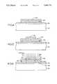
- FIG. 1illustrates the cross section of a conventional polysilicon thin film transistor, the transistor consists of semiconductor or insulator substrate 10, a insulating layer 12 on the top surface of substrate 10, and a thin film polysilicon layer 14 with an overlying insulating layer 21.
- Polysilicon layer 14has a source region 16, a drain region 18, and a channel region 20 therein.
- a polysilicon gate electrode 22overlies the channel region 20.
- the source and drain regionsmust remain stable within polysilicon layer 14.
- An object of the present inventionis to provide an effective process for producing a transistor in a thin polysilicon film, wherein dopant migration in the film is controlled during high temperature process steps.
- Another object of the present inventionis to provide a field effect transistor in a polysilicon thin film that has a consistently better defined channel region due to a modified polysilicon material.
- a polysilicon layeris deposited on an insulating substrate, both N and P type dopants are introduced into the layer in approximately equal concentrations, and insulating layer is formed over the polysilicon layer, a gate electrode is formed over the polysilicon layer, and source and drain regions formed in the polysilicon layer thereby defining the channel region.
- the transistor of the inventionhaving a source region, a drain region and a channel region in a polysilicon layer supported on an insulating substrate, wherein the improvement is providing additional P and N type dopants in the polycrystalline layer in approximately concentrations in excess of 1 ⁇ 10 16 to about 1 ⁇ 10 20 cm. -3 , and uniformly distributed throughout the layer.
- FIG. 1is a sectional view, in greatly exaggerated scale, that illustrates a conventional thin film transistor.
- FIGS. 2 through 6are sectional views, in greatly exaggerated scale, that illustrate the sequential steps for producing the improved thin film transistor of the present invention.
- the present inventionwill be described in detail with reference to this accompanying drawings. It should be noted that the drawings are in greatly simplified form, and illustrate only the transistor structure. In practice, the transistor will be only one of many supported on a common substrate and interconnected with suitable metallurgy into various electronic circuit configurations.
- the substratemay be a monocrystalline semiconductor body with many devices fabricated therein, an is well known in the art, with the transistor formed on a suitable insulating layer in stacked relation to the aforedescribed devices.
- Substrate 30can be of any suitable material, such as silicon, either amorphous, polycrystalline or monocrystalline, glass, quartz, saphire, ceramic, aluminum oxide, etc. Normally the substrate will be provided with an insulating layer 32 on at least the top surface of the substrate 30.
- the layer 30could be a field oxide layer on a monocyrstalline silicon substrate, or a thin oxide layer over associated elements of the device.
- a polycrystalline semiconductor or amorphous semiconductor layer 34is deposited over layer 32 using known technology, such as low pressure chemical vapor deposition, sputter deposition, etc. to the desired thickness.
- the thickness of the polycrystalline layer 34is typically in the range of 500 to 5000 Angstroms, more specifically from 500 to 1,000 Angstroms.
- the semiconductor material of layer 34can be of any type, such as silicon, germanium, gallium arsenide, etc., but is most preferably silicon.
- a first dopant for semiconductorsis then introduced into layer 34, preferably by ion implantation techniques. As illustrated in FIG. 2, boron is implanted, as indicated by arrows 36.
- the dopant concentration in the layer 34is in the range of 1 ⁇ 10 16 to 1 ⁇ 10 20 cm. -3 , more preferably in the range of 5 ⁇ 10 18 to 5 ⁇ 10 19 cm -3 .
- the most preferred techniqueis to ion implant B11 with a dosage of 2 ⁇ 10 14 cm. -2 at an acceleration voltage of about 25 Kev.
- a second opposite type dopant for semiconductorsis introduced into polycrystalline silicon layer 34, as indicated by arrows 38.
- the dopantis of the opposite type of that previously introduced, and in a quantity approximately equal to the first dopant.
- any suitable techniquecan be used to introduce the dopant into the layer. Ion implantation, however, is the preferred technique. The concentration ranges are the same as previously described, the most preferred technique is ion implant P 31 with a dosage of 2 ⁇ 10 14 cm. -2 at an acceleration voltage of 50 Kev.
- an insulating layer 40is formed over the surface of polysilicon layer 34.
- the layer 40can be of any suitable material, and will serve as the gate oxide beneath the gate, which will subsequently be formed.
- layer 40is a thin layer of thermally grown silicon dioxide with a thickness in the range of 200 to 1500 Angstroms, more preferably from 200 to 500 Angstroms.
- the layer 40is formed by heating the polysilicon layer 34 in a dry oxygen environment at a temperature of about 900° C. for a time of 30 minutes.
- layer 40can serve as the complete or a partial anneal thereof.
- Layer 34can be separately annealed, which recrystallizes the polysilicon, by heating it to a temperature in the range of 600° to 1000° C. for a time in the range of 10 to 60 minutes. Most preferably, the anneal of layer 34 is achieved by heating it to a temperature of approximately 900° C. for a time of approximately 30 minutes.
- the polycrystalline silicon material of layer 34is now modified by the introduction of the two opposite type dopants followed by an anneal.
- the average grain size of polysilicon layer 34is about 0.5 micrometers.
- the dopants which include boron and phosphorous atomsare trapped in the grain boundary after the annealing process.
- the grain boundaries with the trapped dopantswill prevent interdiffusion of the dopant from the source 18 and drain 18 regions to be introduced.
- the result of this prevention of interdiffusion between the source and drainwill be stable channel region during and after the back end heat processing. Therefore, the short channel thin film transistor devices which may have a channel of less than about 1.0 micrometers will be manufacturable. Although threshold voltage and carrier mobility will be slightly increased, the operating conditions of these devices are satisfactory.
- the gate electrodeis formed over polysilicon layer 34.
- the gate electrodeis formed by depositing a blanket layer of polysilicon and forming the gate electrode 42 by substrate etching techniques.
- the gate electrode 42will have a thickness in the range of 1000 to 6000 Angstroms, more preferably in the range of 2000 to 4000 Angstroms.
- dopantsare introduced into the polysilicon layer 34, to form the source region 46 and the drain region 48, which define the channel region 50, as indicated by arrows 44. At the same time dopants are introduced into the gate 42 making it electrically conductive.
- the most preferred technique for forming the source and drain regionsis to ion implant B11 with a dosage of 5 ⁇ 10 15 cm. -2 at an acceleration voltage of 25 Kev.
- Another variation of the aforedescribed process of the inventioninvolves hydrogenation of the polysilicon layer 34.
- the hydrogen passivation processis usually carried out after the device process is finished.
- the purpose of this process in the present inventionis to reduce the threshold voltage of the polysilicon thin film transistor.
- the hydrogen ions generated from decomposing ammonia gas by plasma equipmentare combined with dangling bond of silicon atoms located at the grain boundaries to accomplish the passivation of the structure.
- the localized electric fieldwill be largely reduced the resulting in a lowency of the threshold voltage of the polysilicon thin film transistor. This is particularly effective in the present process, because the heat applied during the process will not cause the dopants from the source and drain regions to move into the channel region.
- a polysilicon thin film transistor devicewas fabricated on the silicon substrate 30 with the silicon dioxide layer 32 to prove the operability of the invention.
- the silicon dioxide layerwas 8000 Angstroms in thickness.
- the polysilicon thin film 34 with a thickness of 1000 Angstromswas deposited onto the layer 32 in a low pressure chemical vapor deposition system.
- boron dopant 36was implanted into the polysilcon film.
- the implant dose and energywere 2 ⁇ 10 14 cm. -2 and 25 Kev., respectively.
- An annealing processwas carried out in a nitrogen ambient with temperature and time of 900° C. and 30 minutes, respectively. This produces the FIG. 2 structure.
- Phosphorous ions 38was implanted into the polysilicon layer 34 as seen in FIG. 3.
- the implant dose and energywere 2 ⁇ 10 14 cm. -2 and 25 Kev., respectively.
- the structurewas then annealed in a nitrogen ambient with a temperature of 900° C. and for 30 minutes. After the annealing process was finished, the pattern is etched by lithographic techniques.
- the gate silicon dioxide 40 with a thickness of 350 Angstromswas grown on the polysilicon film 34.
- the growth processwas carried out in a dry oxygen furnace with a temperature of 900° C. and for 30 minutes to produce the FIG. 4 structure.
- the polysilicon gate electrode 42was deposited and doped.
- the gate layer 42 with a thickness of 4500 Angstromswas doped by POCl 3 diffusion to produce conducting electrode.
- the gate patternwas etched by lithographic process techniques. The deposition, POCl 3 diffusion and patterning process is the same as conventional thin film transistor processing. The result of these processes is shown in FIG. 5.
- the boron implantation 44was carried out to form the source 46 and drain 48 regions as shown in FIG. 6.
- the implant dose and energyare 1 ⁇ 10 15 cm. -2 and 25 Kev., respectively.
- the resulting thin film transistorwas tested and found to be satisfactorily operative.
Landscapes
- Engineering & Computer Science (AREA)
- Physics & Mathematics (AREA)
- Condensed Matter Physics & Semiconductors (AREA)
- General Physics & Mathematics (AREA)
- Manufacturing & Machinery (AREA)
- Computer Hardware Design (AREA)
- Microelectronics & Electronic Packaging (AREA)
- Power Engineering (AREA)
- Thin Film Transistor (AREA)
Abstract
Description
Claims (16)
Priority Applications (2)
| Application Number | Priority Date | Filing Date | Title |
|---|---|---|---|
| US07/577,156US5064775A (en) | 1990-09-04 | 1990-09-04 | Method of fabricating an improved polycrystalline silicon thin film transistor |
| US07/742,412US5275872A (en) | 1990-09-04 | 1991-08-08 | Polycrystalline silicon thin film transistor |
Applications Claiming Priority (1)
| Application Number | Priority Date | Filing Date | Title |
|---|---|---|---|
| US07/577,156US5064775A (en) | 1990-09-04 | 1990-09-04 | Method of fabricating an improved polycrystalline silicon thin film transistor |
Related Child Applications (1)
| Application Number | Title | Priority Date | Filing Date |
|---|---|---|---|
| US07/742,412DivisionUS5275872A (en) | 1990-09-04 | 1991-08-08 | Polycrystalline silicon thin film transistor |
Publications (1)
| Publication Number | Publication Date |
|---|---|
| US5064775Atrue US5064775A (en) | 1991-11-12 |
Family
ID=24307498
Family Applications (2)
| Application Number | Title | Priority Date | Filing Date |
|---|---|---|---|
| US07/577,156Expired - LifetimeUS5064775A (en) | 1990-09-04 | 1990-09-04 | Method of fabricating an improved polycrystalline silicon thin film transistor |
| US07/742,412Expired - LifetimeUS5275872A (en) | 1990-09-04 | 1991-08-08 | Polycrystalline silicon thin film transistor |
Family Applications After (1)
| Application Number | Title | Priority Date | Filing Date |
|---|---|---|---|
| US07/742,412Expired - LifetimeUS5275872A (en) | 1990-09-04 | 1991-08-08 | Polycrystalline silicon thin film transistor |
Country Status (1)
| Country | Link |
|---|---|
| US (2) | US5064775A (en) |
Cited By (42)
| Publication number | Priority date | Publication date | Assignee | Title |
|---|---|---|---|---|
| WO1994013009A1 (en)* | 1992-12-01 | 1994-06-09 | Paradigm Technology, Inc. | Transistor fabrication methods and methods of forming multiple layers of photoresist |
| DE4327132A1 (en)* | 1993-08-12 | 1995-03-09 | Siemens Ag | Thin-film transistor and method for production thereof |
| US5397718A (en)* | 1992-02-21 | 1995-03-14 | Matsushita Electric Industrial Co., Ltd. | Method of manufacturing thin film transistor |
| US5403762A (en)* | 1993-06-30 | 1995-04-04 | Semiconductor Energy Laboratory Co., Ltd. | Method of fabricating a TFT |
| US5424230A (en)* | 1992-02-19 | 1995-06-13 | Casio Computer Co., Ltd. | Method of manufacturing a polysilicon thin film transistor |
| US5482871A (en)* | 1994-04-15 | 1996-01-09 | Texas Instruments Incorporated | Method for forming a mesa-isolated SOI transistor having a split-process polysilicon gate |
| US5492843A (en)* | 1993-07-31 | 1996-02-20 | Semiconductor Energy Laboratory Co., Ltd. | Method of fabricating semiconductor device and method of processing substrate |
| US5504019A (en)* | 1990-11-16 | 1996-04-02 | Seiko Epson Corporation | Method for fabricating a thin film semiconductor |
| US5554547A (en)* | 1992-09-29 | 1996-09-10 | Hyundai Electronics Industries Co., Ltd. | Process for the production of thin film transistor using oxygen plasma |
| US5593909A (en)* | 1993-06-25 | 1997-01-14 | Samsung Electronics Co., Ltd. | Method for fabricating a MOS transistor having an offset resistance |
| US5595944A (en)* | 1993-03-12 | 1997-01-21 | Semiconductor Energy Laboratory Co., Inc. | Transistor and process for fabricating the same |
| US5605847A (en)* | 1993-06-24 | 1997-02-25 | Semiconductor Energy Laboratory Co., Ltd. | Process for fabricating a TFT by selectively oxidizing or nitriding a light shielding layer |
| US5670400A (en)* | 1994-12-21 | 1997-09-23 | Samsung Electronics Co., Ltd. | Method for making dual gate insulating film without edge-thinning |
| US5677206A (en)* | 1995-02-24 | 1997-10-14 | Samsung Electronics Co., Ltd. | Method of making a poly-silicon thin film transistor having lightly doped drain structure |
| US5728604A (en)* | 1993-08-19 | 1998-03-17 | Goldstar Electron Co., Ltd. | Method for making thin film transistors |
| US5756371A (en)* | 1992-11-18 | 1998-05-26 | Nippon Sheet Glass Co., Ltd. | Process of producing thin film transistor array |
| US5841931A (en)* | 1996-11-26 | 1998-11-24 | Massachusetts Institute Of Technology | Methods of forming polycrystalline semiconductor waveguides for optoelectronic integrated circuits, and devices formed thereby |
| US5846871A (en)* | 1997-08-26 | 1998-12-08 | Lucent Technologies Inc. | Integrated circuit fabrication |
| US5861335A (en)* | 1997-03-21 | 1999-01-19 | Advanced Micro Devices, Inc. | Semiconductor fabrication employing a post-implant anneal within a low temperature high pressure nitrogen ambient to improve channel and gate oxide reliability |
| US5932919A (en)* | 1993-12-07 | 1999-08-03 | Siemens Aktiengesellschaft | MOSFETs with improved short channel effects |
| US6051865A (en)* | 1998-11-09 | 2000-04-18 | Advanced Micro Devices, Inc. | Transistor having a barrier layer below a high permittivity gate dielectric |
| US6127210A (en)* | 1995-10-16 | 2000-10-03 | Hitachi, Ltd. | Manufacturing method of CMOS thin film semiconductor device and CMOS thin film semiconductor device manufactured thereby |
| US6165876A (en)* | 1995-01-30 | 2000-12-26 | Yamazaki; Shunpei | Method of doping crystalline silicon film |
| US6261875B1 (en) | 1993-03-12 | 2001-07-17 | Semiconductor Energy Laboratory Co., Ltd. | Transistor and process for fabricating the same |
| US20010034089A1 (en)* | 2000-01-20 | 2001-10-25 | Shunpei Yamazaki | Method of manufacturing a semiconductor device |
| US6323071B1 (en) | 1992-12-04 | 2001-11-27 | Semiconductor Energy Laboratory Co., Ltd. | Method for forming a semiconductor device |
| US6441399B1 (en) | 1994-04-22 | 2002-08-27 | Semiconductor Energy Laboratory Co., Ltd. | Semiconductor integrated system |
| US6455875B2 (en) | 1992-10-09 | 2002-09-24 | Semiconductor Energy Laboratory Co., Ltd. | Thin film transistor having enhanced field mobility |
| US20020142525A1 (en)* | 2001-01-26 | 2002-10-03 | Hideto Ohnuma | Method of manufacturing semiconductor device |
| US6624477B1 (en) | 1992-10-09 | 2003-09-23 | Semiconductor Energy Laboratory Co., Ltd. | Semiconductor device and method for manufacturing the same |
| US20030217620A1 (en)* | 2002-04-08 | 2003-11-27 | Council Scientific And Industrial Research | Process for the production of neodymium-iron-boron permanent magnet alloy powder |
| US20040038465A1 (en)* | 2002-06-28 | 2004-02-26 | Akihisa Shimomura | Method of manufacturing a semiconductor device |
| US6960498B2 (en) | 2002-07-04 | 2005-11-01 | Semiconductor Energy Laboratory Co., Ltd. | Doping method, doping apparatus, and control system for doping apparatus |
| US6964890B1 (en)* | 1992-03-17 | 2005-11-15 | Semiconductor Energy Laboratory Co., Ltd. | Semiconductor device and method for forming the same |
| US20060177996A1 (en)* | 2005-02-10 | 2006-08-10 | Semiconductor Energy Laboratory Co., Ltd. | Doping method and method of manufacturing field effect transistor |
| US7291003B1 (en)* | 2004-09-23 | 2007-11-06 | Sandia Corporation | Micromachined spinneret |
| US20080160735A1 (en)* | 2006-12-28 | 2008-07-03 | Qimonda Ag | Forming Polysilicon Regions |
| US20090098690A1 (en)* | 2007-10-10 | 2009-04-16 | Semiconductor Energy Laboratory Co., Ltd. | Manufacturing method of semiconductor device |
| US20090191694A1 (en)* | 2008-01-24 | 2009-07-30 | Semiconductor Energy Laboratory Co., Ltd. | Manufacturing method of semiconductor substrate |
| CN1893001B (en)* | 1993-03-12 | 2011-10-05 | 株式会社半导体能源研究所 | Method for manufacturing semiconductor device |
| US8455331B2 (en) | 2007-10-10 | 2013-06-04 | Semiconductor Energy Laboratory Co., Ltd. | Manufacturing method of semiconductor device |
| US20230112644A1 (en)* | 2021-09-30 | 2023-04-13 | Texas Instruments Incorporated | Carbon and/or Oxygen Doped Polysilicon Resistor |
Families Citing this family (8)
| Publication number | Priority date | Publication date | Assignee | Title |
|---|---|---|---|---|
| US5854494A (en)* | 1991-02-16 | 1998-12-29 | Semiconductor Energy Laboratory Co., Ltd. | Electric device, matrix device, electro-optical display device, and semiconductor memory having thin-film transistors |
| US6028333A (en)* | 1991-02-16 | 2000-02-22 | Semiconductor Energy Laboratory Co., Ltd. | Electric device, matrix device, electro-optical display device, and semiconductor memory having thin-film transistors |
| JP3556679B2 (en) | 1992-05-29 | 2004-08-18 | 株式会社半導体エネルギー研究所 | Electro-optical device |
| US6709907B1 (en)* | 1992-02-25 | 2004-03-23 | Semiconductor Energy Laboratory Co., Ltd. | Method of fabricating a thin film transistor |
| TW222345B (en)* | 1992-02-25 | 1994-04-11 | Semicondustor Energy Res Co Ltd | Semiconductor and its manufacturing method |
| JP2908150B2 (en)* | 1992-11-27 | 1999-06-21 | 日本電気株式会社 | SOI substrate structure and manufacturing method thereof |
| US6943764B1 (en)* | 1994-04-22 | 2005-09-13 | Semiconductor Energy Laboratory Co., Ltd. | Driver circuit for an active matrix display device |
| US6709910B1 (en)* | 2002-10-18 | 2004-03-23 | Sharp Laboratories Of America, Inc. | Method for reducing surface protrusions in the fabrication of lilac films |
Citations (10)
| Publication number | Priority date | Publication date | Assignee | Title |
|---|---|---|---|---|
| US4054895A (en)* | 1976-12-27 | 1977-10-18 | Rca Corporation | Silicon-on-sapphire mesa transistor having doped edges |
| US4178191A (en)* | 1978-08-10 | 1979-12-11 | Rca Corp. | Process of making a planar MOS silicon-on-insulating substrate device |
| US4489104A (en)* | 1983-06-03 | 1984-12-18 | Industrial Technology Research Institute | Polycrystalline silicon resistor having limited lateral diffusion |
| US4624737A (en)* | 1984-08-21 | 1986-11-25 | Seiko Instruments & Electronics Ltd. | Process for producing thin-film transistor |
| US4637836A (en)* | 1985-09-23 | 1987-01-20 | Rca Corporation | Profile control of boron implant |
| US4682407A (en)* | 1986-01-21 | 1987-07-28 | Motorola, Inc. | Means and method for stabilizing polycrystalline semiconductor layers |
| US4737471A (en)* | 1985-06-19 | 1988-04-12 | Fujitsu Limited | Method for fabricating an insulated-gate FET having a narrow channel width |
| US4762803A (en)* | 1984-12-07 | 1988-08-09 | Fuji Electric Co., Ltd. | Process for forming crystalline films by glow discharge |
| US4772927A (en)* | 1985-10-23 | 1988-09-20 | Hitachi, Ltd. | Thin film FET doped with diffusion inhibitor |
| US4866006A (en)* | 1985-06-03 | 1989-09-12 | Toyo Boseki Kabushiki Kaisha | Process for producing hydrogenated amorphous silicon film |
Family Cites Families (1)
| Publication number | Priority date | Publication date | Assignee | Title |
|---|---|---|---|---|
| US4673531A (en)* | 1983-06-03 | 1987-06-16 | Industrial Technology Research Institute | Polycrystalline silicon resistor having limited lateral diffusion |
- 1990
- 1990-09-04USUS07/577,156patent/US5064775A/ennot_activeExpired - Lifetime
- 1991
- 1991-08-08USUS07/742,412patent/US5275872A/ennot_activeExpired - Lifetime
Patent Citations (10)
| Publication number | Priority date | Publication date | Assignee | Title |
|---|---|---|---|---|
| US4054895A (en)* | 1976-12-27 | 1977-10-18 | Rca Corporation | Silicon-on-sapphire mesa transistor having doped edges |
| US4178191A (en)* | 1978-08-10 | 1979-12-11 | Rca Corp. | Process of making a planar MOS silicon-on-insulating substrate device |
| US4489104A (en)* | 1983-06-03 | 1984-12-18 | Industrial Technology Research Institute | Polycrystalline silicon resistor having limited lateral diffusion |
| US4624737A (en)* | 1984-08-21 | 1986-11-25 | Seiko Instruments & Electronics Ltd. | Process for producing thin-film transistor |
| US4762803A (en)* | 1984-12-07 | 1988-08-09 | Fuji Electric Co., Ltd. | Process for forming crystalline films by glow discharge |
| US4866006A (en)* | 1985-06-03 | 1989-09-12 | Toyo Boseki Kabushiki Kaisha | Process for producing hydrogenated amorphous silicon film |
| US4737471A (en)* | 1985-06-19 | 1988-04-12 | Fujitsu Limited | Method for fabricating an insulated-gate FET having a narrow channel width |
| US4637836A (en)* | 1985-09-23 | 1987-01-20 | Rca Corporation | Profile control of boron implant |
| US4772927A (en)* | 1985-10-23 | 1988-09-20 | Hitachi, Ltd. | Thin film FET doped with diffusion inhibitor |
| US4682407A (en)* | 1986-01-21 | 1987-07-28 | Motorola, Inc. | Means and method for stabilizing polycrystalline semiconductor layers |
Non-Patent Citations (4)
| Title |
|---|
| Hawkins, W., "Polycrystalline-Silicon Device Technology . . .", IEEE Trans. Electron Devices, vol. ED. 33, No. 4, Apr. 1986, pp. 477-481. |
| Hawkins, W., Polycrystalline Silicon Device Technology . . . , IEEE Trans. Electron Devices, vol. ED. 33, No. 4, Apr. 1986, pp. 477 481.* |
| Lee et al., "On the Semi-Insulating Polycrystalline Silicon Resistor", Solid-State Electronics, vol. 27, No. 11, 1984, pp. 995-1001. |
| Lee et al., On the Semi Insulating Polycrystalline Silicon Resistor , Solid State Electronics, vol. 27, No. 11, 1984, pp. 995 1001.* |
Cited By (97)
| Publication number | Priority date | Publication date | Assignee | Title |
|---|---|---|---|---|
| US5504019A (en)* | 1990-11-16 | 1996-04-02 | Seiko Epson Corporation | Method for fabricating a thin film semiconductor |
| US5424230A (en)* | 1992-02-19 | 1995-06-13 | Casio Computer Co., Ltd. | Method of manufacturing a polysilicon thin film transistor |
| US5397718A (en)* | 1992-02-21 | 1995-03-14 | Matsushita Electric Industrial Co., Ltd. | Method of manufacturing thin film transistor |
| US6964890B1 (en)* | 1992-03-17 | 2005-11-15 | Semiconductor Energy Laboratory Co., Ltd. | Semiconductor device and method for forming the same |
| US7564057B1 (en) | 1992-03-17 | 2009-07-21 | Semiconductor Energy Laboratory Co., Ltd. | Semiconductor device having an aluminum nitride film |
| US5554547A (en)* | 1992-09-29 | 1996-09-10 | Hyundai Electronics Industries Co., Ltd. | Process for the production of thin film transistor using oxygen plasma |
| US7109108B2 (en) | 1992-10-09 | 2006-09-19 | Semiconductor Energy Laboratory Co., Ltd. | Method for manufacturing semiconductor device having metal silicide |
| US20090152631A1 (en)* | 1992-10-09 | 2009-06-18 | Semiconductor Energy Laboratory Co., Ltd. | Semiconductor device and method for forming the same |
| US7602020B2 (en) | 1992-10-09 | 2009-10-13 | Semiconductor Energy Laboratory Co., Ltd. | Semiconductor device and method for forming the same |
| US7723788B2 (en) | 1992-10-09 | 2010-05-25 | Semiconductor Energy Laboratory Co., Ltd. | Semiconductor device and method for forming the same |
| US20030006414A1 (en)* | 1992-10-09 | 2003-01-09 | Semiconductor Energy Laboratory Co., Ltd. | Semiconductor device and method for forming the same |
| US8017506B2 (en) | 1992-10-09 | 2011-09-13 | Semiconductor Energy Laboratory Co., Ltd. | Semiconductor device and method for forming the same |
| US6790749B2 (en) | 1992-10-09 | 2004-09-14 | Semiconductor Energy Laboratory Co., Ltd. | Method of manufacturing a semiconductor device |
| US6624477B1 (en) | 1992-10-09 | 2003-09-23 | Semiconductor Energy Laboratory Co., Ltd. | Semiconductor device and method for manufacturing the same |
| US6455875B2 (en) | 1992-10-09 | 2002-09-24 | Semiconductor Energy Laboratory Co., Ltd. | Thin film transistor having enhanced field mobility |
| US20050037549A1 (en)* | 1992-10-09 | 2005-02-17 | Semiconductor Energy Laboratory Co., Ltd. | Semiconductor device and method for forming the same |
| US20100041187A1 (en)* | 1992-10-09 | 2010-02-18 | Semiconductor Energy Laboratory Co., Ltd. | Semiconductor device and method for forming the same |
| US5756371A (en)* | 1992-11-18 | 1998-05-26 | Nippon Sheet Glass Co., Ltd. | Process of producing thin film transistor array |
| WO1994013009A1 (en)* | 1992-12-01 | 1994-06-09 | Paradigm Technology, Inc. | Transistor fabrication methods and methods of forming multiple layers of photoresist |
| US5348897A (en)* | 1992-12-01 | 1994-09-20 | Paradigm Technology, Inc. | Transistor fabrication methods using overlapping masks |
| US20030036222A1 (en)* | 1992-12-04 | 2003-02-20 | Semiconductor Energy Laboratory Co., Ltd. | Semiconductor device and method of fabricating the same |
| US6323071B1 (en) | 1992-12-04 | 2001-11-27 | Semiconductor Energy Laboratory Co., Ltd. | Method for forming a semiconductor device |
| US6338991B1 (en) | 1992-12-04 | 2002-01-15 | Semiconductor Energy Laboratory Co., Ltd. | Semiconductor device and method for manufacturing the same |
| US7622335B2 (en) | 1992-12-04 | 2009-11-24 | Semiconductor Energy Laboratory Co., Ltd. | Method for manufacturing a thin film transistor device |
| US6872605B2 (en) | 1992-12-04 | 2005-03-29 | Semiconductor Energy Laboratory Co., Ltd. | Semiconductor device and method of fabricating the same |
| US8062935B2 (en) | 1992-12-04 | 2011-11-22 | Semiconductor Energy Laboratory Co., Ltd. | Semiconductor device and method for manufacturing the same |
| US8278660B2 (en) | 1992-12-04 | 2012-10-02 | Semiconductor Energy Laboratory Co., Ltd. | Semiconductor device and method for manufacturing the same |
| US6806125B2 (en) | 1992-12-04 | 2004-10-19 | Semiconductor Energy Laboratory Co., Ltd. | Method of manufacturing a thin film transistor device |
| US6261875B1 (en) | 1993-03-12 | 2001-07-17 | Semiconductor Energy Laboratory Co., Ltd. | Transistor and process for fabricating the same |
| US6060725A (en)* | 1993-03-12 | 2000-05-09 | Semiconductor Energy Laboratory Co., Ltd. | Thin film transistor using a semiconductor film |
| US6939749B2 (en) | 1993-03-12 | 2005-09-06 | Semiconductor Energy Laboratory Co., Ltd | Method of manufacturing a semiconductor device that includes heating the gate insulating film |
| CN1893000B (en)* | 1993-03-12 | 2012-06-27 | 株式会社半导体能源研究所 | Method for manufacturing semiconductor device |
| CN1542929B (en)* | 1993-03-12 | 2012-05-30 | 株式会社半导体能源研究所 | Manufacturing method of semiconductor device |
| CN1893001B (en)* | 1993-03-12 | 2011-10-05 | 株式会社半导体能源研究所 | Method for manufacturing semiconductor device |
| US6541313B2 (en) | 1993-03-12 | 2003-04-01 | Semiconductor Energy Laboratory Co., Ltd. | Transistor and process for fabricating the same |
| US5595944A (en)* | 1993-03-12 | 1997-01-21 | Semiconductor Energy Laboratory Co., Inc. | Transistor and process for fabricating the same |
| US6335540B1 (en) | 1993-06-24 | 2002-01-01 | Semiconductor Energy Laboratory Co., Ltd. | Semiconductor device and process for fabricating the same |
| US6573589B2 (en) | 1993-06-24 | 2003-06-03 | Semiconductor Energy Laboratory Co., Ltd. | Semiconductor device and process for fabricating the same |
| US5605847A (en)* | 1993-06-24 | 1997-02-25 | Semiconductor Energy Laboratory Co., Ltd. | Process for fabricating a TFT by selectively oxidizing or nitriding a light shielding layer |
| US5894157A (en)* | 1993-06-25 | 1999-04-13 | Samsung Electronics Co., Ltd. | MOS transistor having an offset resistance derived from a multiple region gate electrode |
| US5593909A (en)* | 1993-06-25 | 1997-01-14 | Samsung Electronics Co., Ltd. | Method for fabricating a MOS transistor having an offset resistance |
| US6479331B1 (en) | 1993-06-30 | 2002-11-12 | Semiconductor Energy Laboratory Co., Ltd. | Method of fabricating a semiconductor device |
| US7238558B2 (en) | 1993-06-30 | 2007-07-03 | Semiconductor Energy Laboratory Co., Ltd. | Semiconductor device and method of fabricating the same |
| US5403762A (en)* | 1993-06-30 | 1995-04-04 | Semiconductor Energy Laboratory Co., Ltd. | Method of fabricating a TFT |
| US5572046A (en)* | 1993-06-30 | 1996-11-05 | Semiconductor Energy Laboratory Co., Ltd. | Semiconductor device having at least two thin film transistors |
| US5492843A (en)* | 1993-07-31 | 1996-02-20 | Semiconductor Energy Laboratory Co., Ltd. | Method of fabricating semiconductor device and method of processing substrate |
| US5837619A (en)* | 1993-07-31 | 1998-11-17 | Semiconductor Energy Laboratory Co., Ltd. | Method of fabricating semiconductor device and method of processing substrate |
| DE4327132A1 (en)* | 1993-08-12 | 1995-03-09 | Siemens Ag | Thin-film transistor and method for production thereof |
| US5528053A (en)* | 1993-08-12 | 1996-06-18 | Siemens Aktiengesellschaft | Thin-film transistor and method for the manufacture thereof |
| US5728604A (en)* | 1993-08-19 | 1998-03-17 | Goldstar Electron Co., Ltd. | Method for making thin film transistors |
| US5932919A (en)* | 1993-12-07 | 1999-08-03 | Siemens Aktiengesellschaft | MOSFETs with improved short channel effects |
| US5482871A (en)* | 1994-04-15 | 1996-01-09 | Texas Instruments Incorporated | Method for forming a mesa-isolated SOI transistor having a split-process polysilicon gate |
| US20020195634A1 (en)* | 1994-04-22 | 2002-12-26 | Semiconductor Energy Laboratory Co., Ltd. | Semiconductor integrated circuit |
| US7145173B2 (en) | 1994-04-22 | 2006-12-05 | Semiconductor Energy Laboratory Co., Ltd. | Semiconductor integrated circuit |
| US20050139831A1 (en)* | 1994-04-22 | 2005-06-30 | Semiconductor Energy | Semiconductor integrated circuit |
| US6599791B1 (en) | 1994-04-22 | 2003-07-29 | Semiconductor Energy Laboratory Co., Ltd. | Semiconductor integrated circuit |
| US6441399B1 (en) | 1994-04-22 | 2002-08-27 | Semiconductor Energy Laboratory Co., Ltd. | Semiconductor integrated system |
| US7166862B2 (en) | 1994-04-22 | 2007-01-23 | Semiconductor Energy Laboratory Co., Ltd. | Semiconductor integrated circuit |
| US5670400A (en)* | 1994-12-21 | 1997-09-23 | Samsung Electronics Co., Ltd. | Method for making dual gate insulating film without edge-thinning |
| US6165876A (en)* | 1995-01-30 | 2000-12-26 | Yamazaki; Shunpei | Method of doping crystalline silicon film |
| US5677206A (en)* | 1995-02-24 | 1997-10-14 | Samsung Electronics Co., Ltd. | Method of making a poly-silicon thin film transistor having lightly doped drain structure |
| US6127210A (en)* | 1995-10-16 | 2000-10-03 | Hitachi, Ltd. | Manufacturing method of CMOS thin film semiconductor device and CMOS thin film semiconductor device manufactured thereby |
| US6108464A (en)* | 1996-11-26 | 2000-08-22 | Massachusetts Institute Of Technology | Optoelectronic integrated circuits formed of polycrystalline semiconductor waveguide |
| US5841931A (en)* | 1996-11-26 | 1998-11-24 | Massachusetts Institute Of Technology | Methods of forming polycrystalline semiconductor waveguides for optoelectronic integrated circuits, and devices formed thereby |
| US6288432B1 (en) | 1997-03-21 | 2001-09-11 | Advanced Micro Devices, Inc. | Semiconductor fabrication employing a post-implant anneal within a low temperature, high pressure nitrogen ambient to improve channel and gate oxide reliability |
| US5861335A (en)* | 1997-03-21 | 1999-01-19 | Advanced Micro Devices, Inc. | Semiconductor fabrication employing a post-implant anneal within a low temperature high pressure nitrogen ambient to improve channel and gate oxide reliability |
| US5846871A (en)* | 1997-08-26 | 1998-12-08 | Lucent Technologies Inc. | Integrated circuit fabrication |
| US6051865A (en)* | 1998-11-09 | 2000-04-18 | Advanced Micro Devices, Inc. | Transistor having a barrier layer below a high permittivity gate dielectric |
| US7071041B2 (en)* | 2000-01-20 | 2006-07-04 | Semiconductor Energy Laboratory Co., Ltd. | Method of manufacturing a semiconductor device |
| US20060220021A1 (en)* | 2000-01-20 | 2006-10-05 | Semiconductor Energy Laboratory Co., Ltd. | Method of manufacturing a semiconductor device |
| US7429751B2 (en) | 2000-01-20 | 2008-09-30 | Semiconductor Energy Laboratory Co., Ltd. | Method of manufacturing a semiconductor device |
| US20010034089A1 (en)* | 2000-01-20 | 2001-10-25 | Shunpei Yamazaki | Method of manufacturing a semiconductor device |
| US20070072350A1 (en)* | 2001-01-26 | 2007-03-29 | Semiconductor Energy Laboratory Co., Ltd. | Method of manufacturing semiconductor device |
| US7361577B2 (en) | 2001-01-26 | 2008-04-22 | Semiconductor Energy Laboratory Co., Ltd. | Method of manufacturing semiconductor device |
| US7151017B2 (en) | 2001-01-26 | 2006-12-19 | Semiconductor Energy Laboratory Co., Ltd. | Method of manufacturing semiconductor device |
| US20020142525A1 (en)* | 2001-01-26 | 2002-10-03 | Hideto Ohnuma | Method of manufacturing semiconductor device |
| US20030217620A1 (en)* | 2002-04-08 | 2003-11-27 | Council Scientific And Industrial Research | Process for the production of neodymium-iron-boron permanent magnet alloy powder |
| US7329594B2 (en) | 2002-06-28 | 2008-02-12 | Semiconductor Energy Laboratory Co., Ltd. | Method of manufacturing a semiconductor device |
| US20040038465A1 (en)* | 2002-06-28 | 2004-02-26 | Akihisa Shimomura | Method of manufacturing a semiconductor device |
| US7534705B2 (en) | 2002-06-28 | 2009-05-19 | Semiconductor Energy Laboratory Co., Ltd. | Method of manufacturing a semiconductor device |
| US20080070352A1 (en)* | 2002-06-28 | 2008-03-20 | Semiconductor Energy Laboratory Co., Ltd. | Method of manufacturing a semiconductor device |
| US6960498B2 (en) | 2002-07-04 | 2005-11-01 | Semiconductor Energy Laboratory Co., Ltd. | Doping method, doping apparatus, and control system for doping apparatus |
| US20060005768A1 (en)* | 2002-07-04 | 2006-01-12 | Semiconductor Energy Laboratory Co., Ltd. | Doping method, doping apparatus, and control system for doping apparatus |
| US7361912B2 (en) | 2002-07-04 | 2008-04-22 | Semiconductor Energy Laboratory Co., Ltd. | Doping method, doping apparatus, and control system for doping apparatus |
| US7291003B1 (en)* | 2004-09-23 | 2007-11-06 | Sandia Corporation | Micromachined spinneret |
| US20060177996A1 (en)* | 2005-02-10 | 2006-08-10 | Semiconductor Energy Laboratory Co., Ltd. | Doping method and method of manufacturing field effect transistor |
| US7442631B2 (en) | 2005-02-10 | 2008-10-28 | Semiconductor Energy Laboratory Co., Ltd. | Doping method and method of manufacturing field effect transistor |
| US20080160735A1 (en)* | 2006-12-28 | 2008-07-03 | Qimonda Ag | Forming Polysilicon Regions |
| US20090098690A1 (en)* | 2007-10-10 | 2009-04-16 | Semiconductor Energy Laboratory Co., Ltd. | Manufacturing method of semiconductor device |
| US8455331B2 (en) | 2007-10-10 | 2013-06-04 | Semiconductor Energy Laboratory Co., Ltd. | Manufacturing method of semiconductor device |
| US8501585B2 (en) | 2007-10-10 | 2013-08-06 | Semiconductor Energy Laboratory Co., Ltd. | Manufacturing method of semiconductor device |
| US20110151593A1 (en)* | 2008-01-24 | 2011-06-23 | Semiconductor Energy Laboratory Co., Ltd. | Manufacturing method of semiconductor substrate |
| US7910465B2 (en) | 2008-01-24 | 2011-03-22 | Semiconductor Energy Laboratory Co., Ltd. | Manufacturing method of semiconductor substrate |
| US20090191694A1 (en)* | 2008-01-24 | 2009-07-30 | Semiconductor Energy Laboratory Co., Ltd. | Manufacturing method of semiconductor substrate |
| US8492248B2 (en) | 2008-01-24 | 2013-07-23 | Semiconductor Energy Laboratory Co., Ltd. | Manufacturing method of semiconductor substrate |
| US20230112644A1 (en)* | 2021-09-30 | 2023-04-13 | Texas Instruments Incorporated | Carbon and/or Oxygen Doped Polysilicon Resistor |
| US12027515B2 (en)* | 2021-09-30 | 2024-07-02 | Texas Instruments Incorporated | Carbon and/or oxygen doped polysilicon resistor |
Also Published As
| Publication number | Publication date |
|---|---|
| US5275872A (en) | 1994-01-04 |
Similar Documents
| Publication | Publication Date | Title |
|---|---|---|
| US5064775A (en) | Method of fabricating an improved polycrystalline silicon thin film transistor | |
| US6162711A (en) | In-situ boron doped polysilicon with dual layer and dual grain structure for use in integrated circuits manufacturing | |
| EP0090963B1 (en) | Method for making polycrystalline silicon film resistors | |
| US6331468B1 (en) | Formation of integrated circuit structure using one or more silicon layers for implantation and out-diffusion in formation of defect-free source/drain regions and also for subsequent formation of silicon nitride spacers | |
| US5326722A (en) | Polysilicon contact | |
| US5338697A (en) | Doping method of barrier region in semiconductor device | |
| US4808546A (en) | SOI process for forming a thin film transistor using solid phase epitaxy | |
| JPH0777259B2 (en) | Method for manufacturing polycrystalline silicon resistor having desired temperature coefficient | |
| US5015593A (en) | Method of manufacturing semiconductor device | |
| US5712181A (en) | Method for the formation of polycide gate in semiconductor device | |
| EP0051500B1 (en) | Semiconductor devices | |
| US4354307A (en) | Method for mass producing miniature field effect transistors in high density LSI/VLSI chips | |
| JP2947828B2 (en) | Method for manufacturing semiconductor device | |
| US4502894A (en) | Method of fabricating polycrystalline silicon resistors in integrated circuit structures using outdiffusion | |
| US5310711A (en) | Method of forming doped shallow electrical junctions | |
| JPS61229346A (en) | Formation of polychrystal silicon on integrated circuit | |
| JP3313432B2 (en) | Semiconductor device and manufacturing method thereof | |
| US4891332A (en) | Method of manufacturing a semiconductor device comprising a circuit element formed of carbon doped polycrystalline silicon | |
| JPH03116875A (en) | Thin film field effect transistor and method of manufacturing the same | |
| US4826779A (en) | Integrated capacitor and method of fabricating same | |
| US5491107A (en) | Semiconductor processing method for providing large grain polysilicon films | |
| JPH10125919A (en) | Method for forming electrode of semiconductor element | |
| JP3116163B2 (en) | Method of manufacturing insulated gate field effect transistor | |
| US4954454A (en) | Method for fabricating a polycrystalline silicon resistor | |
| JP2797200B2 (en) | Polycrystalline silicon electrode and method of manufacturing the same |
Legal Events
| Date | Code | Title | Description |
|---|---|---|---|
| AS | Assignment | Owner name:INDUSTRIAL TECHNOLOGY RESEARCH INSTITUTE, TAIWAN Free format text:ASSIGNMENT OF ASSIGNORS INTEREST.;ASSIGNOR:CHANG, KUN-ZEN;REEL/FRAME:005431/0667 Effective date:19900824 | |
| STCF | Information on status: patent grant | Free format text:PATENTED CASE | |
| FEPP | Fee payment procedure | Free format text:PAT HLDR NO LONGER CLAIMS SMALL ENT STAT AS SMALL BUSINESS (ORIGINAL EVENT CODE: LSM2); ENTITY STATUS OF PATENT OWNER: LARGE ENTITY | |
| FPAY | Fee payment | Year of fee payment:4 | |
| REMI | Maintenance fee reminder mailed | ||
| FPAY | Fee payment | Year of fee payment:8 | |
| SULP | Surcharge for late payment | ||
| AS | Assignment | Owner name:AU OPTRONICS CORP., TAIWAN Free format text:ASSIGNMENT OF ASSIGNORS INTEREST;ASSIGNOR:INDUSTRIAL TECHNOLOGY RESEARCH INSTITUTE;REEL/FRAME:013740/0654 Effective date:20020724 Owner name:CHI MEI OPTOELECTRONICS CORP., TAIWAN Free format text:ASSIGNMENT OF ASSIGNORS INTEREST;ASSIGNOR:INDUSTRIAL TECHNOLOGY RESEARCH INSTITUTE;REEL/FRAME:013740/0654 Effective date:20020724 Owner name:CHUNGHWA PICTURE TUBES, LTD., TAIWAN Free format text:ASSIGNMENT OF ASSIGNORS INTEREST;ASSIGNOR:INDUSTRIAL TECHNOLOGY RESEARCH INSTITUTE;REEL/FRAME:013740/0654 Effective date:20020724 Owner name:HANNSTAR DISPLAY CORP., TAIWAN Free format text:ASSIGNMENT OF ASSIGNORS INTEREST;ASSIGNOR:INDUSTRIAL TECHNOLOGY RESEARCH INSTITUTE;REEL/FRAME:013740/0654 Effective date:20020724 Owner name:INDUSTRIAL TECHNOLOGY RESEARCH INSTITUTE, TAIWAN Free format text:ASSIGNMENT OF ASSIGNORS INTEREST;ASSIGNOR:INDUSTRIAL TECHNOLOGY RESEARCH INSTITUTE;REEL/FRAME:013740/0654 Effective date:20020724 Owner name:PRIME VIEW INTERNATIONAL CO., LTD., TAIWAN Free format text:ASSIGNMENT OF ASSIGNORS INTEREST;ASSIGNOR:INDUSTRIAL TECHNOLOGY RESEARCH INSTITUTE;REEL/FRAME:013740/0654 Effective date:20020724 Owner name:QUANTA DISPLAY INC., TAIWAN Free format text:ASSIGNMENT OF ASSIGNORS INTEREST;ASSIGNOR:INDUSTRIAL TECHNOLOGY RESEARCH INSTITUTE;REEL/FRAME:013740/0654 Effective date:20020724 Owner name:TOPPOLY OPTOELECTRONICS CORP., TAIWAN Free format text:ASSIGNMENT OF ASSIGNORS INTEREST;ASSIGNOR:INDUSTRIAL TECHNOLOGY RESEARCH INSTITUTE;REEL/FRAME:013740/0654 Effective date:20020724 | |
| FPAY | Fee payment | Year of fee payment:12 | |
| AS | Assignment | Owner name:INDUSTRIAL TECHNOLOGY RESEARCH INSTITUTE, TAIWAN Free format text:ASSIGNMENT OF ASSIGNORS INTEREST;ASSIGNORS:INDUSTRIAL TECHNOLOGY RESEARCH INSTITUTE;AU OPTRONICS CORP.;CHUNGHWA PICTURE TUBES, LTD.;AND OTHERS;REEL/FRAME:023234/0930 Effective date:20090520 |