US5064685A - Electrical conductor deposition method - Google Patents
Electrical conductor deposition methodDownload PDFInfo
- Publication number
- US5064685A US5064685AUS07/397,700US39770089AUS5064685AUS 5064685 AUS5064685 AUS 5064685AUS 39770089 AUS39770089 AUS 39770089AUS 5064685 AUS5064685 AUS 5064685A
- Authority
- US
- United States
- Prior art keywords
- substrate
- metal
- organic compound
- power
- laser beam
- Prior art date
- Legal status (The legal status is an assumption and is not a legal conclusion. Google has not performed a legal analysis and makes no representation as to the accuracy of the status listed.)
- Expired - Lifetime
Links
- 238000000151depositionMethods0.000titleclaimsdescription28
- 239000004020conductorSubstances0.000titledescription27
- 239000000758substrateSubstances0.000claimsabstractdescription88
- 150000002902organometallic compoundsChemical class0.000claimsabstractdescription20
- 230000005855radiationEffects0.000claimsabstractdescription7
- 238000000034methodMethods0.000claimsdescription27
- 239000002184metalSubstances0.000claimsdescription21
- VYPSYNLAJGMNEJ-UHFFFAOYSA-NSilicium dioxideChemical compoundO=[Si]=OVYPSYNLAJGMNEJ-UHFFFAOYSA-N0.000claimsdescription20
- 230000008021depositionEffects0.000claimsdescription20
- 229910052751metalInorganic materials0.000claimsdescription20
- 239000010931goldSubstances0.000claimsdescription16
- 229910052737goldInorganic materials0.000claimsdescription16
- PCHJSUWPFVWCPO-UHFFFAOYSA-NgoldChemical compound[Au]PCHJSUWPFVWCPO-UHFFFAOYSA-N0.000claimsdescription13
- 239000000463materialSubstances0.000claimsdescription10
- 239000000377silicon dioxideSubstances0.000claimsdescription10
- 235000012239silicon dioxideNutrition0.000claimsdescription10
- 150000001875compoundsChemical class0.000claimsdescription2
- 239000011532electronic conductorSubstances0.000claims3
- 230000001464adherent effectEffects0.000claims1
- 238000001465metallisationMethods0.000abstractdescription3
- 239000004065semiconductorSubstances0.000description9
- 230000008569processEffects0.000description5
- 239000004642PolyimideSubstances0.000description4
- 230000008859changeEffects0.000description4
- 229920001721polyimidePolymers0.000description4
- 238000000197pyrolysisMethods0.000description4
- XKRFYHLGVUSROY-UHFFFAOYSA-NargonSubstances[Ar]XKRFYHLGVUSROY-UHFFFAOYSA-N0.000description3
- XUIMIQQOPSSXEZ-UHFFFAOYSA-NSiliconChemical compound[Si]XUIMIQQOPSSXEZ-UHFFFAOYSA-N0.000description2
- 229910052786argonInorganic materials0.000description2
- 230000007547defectEffects0.000description2
- 238000002474experimental methodMethods0.000description2
- 238000005001rutherford backscattering spectroscopyMethods0.000description2
- OKTJSMMVPCPJKN-UHFFFAOYSA-NCarbonChemical compound[C]OKTJSMMVPCPJKN-UHFFFAOYSA-N0.000description1
- 241001363516Plusia festucaeSpecies0.000description1
- NINIDFKCEFEMDL-UHFFFAOYSA-NSulfurChemical compound[S]NINIDFKCEFEMDL-UHFFFAOYSA-N0.000description1
- RTAQQCXQSZGOHL-UHFFFAOYSA-NTitaniumChemical compound[Ti]RTAQQCXQSZGOHL-UHFFFAOYSA-N0.000description1
- 239000000654additiveSubstances0.000description1
- 238000004458analytical methodMethods0.000description1
- 238000013459approachMethods0.000description1
- QVGXLLKOCUKJST-UHFFFAOYSA-Natomic oxygenChemical compound[O]QVGXLLKOCUKJST-UHFFFAOYSA-N0.000description1
- 239000010953base metalSubstances0.000description1
- 229910052799carbonInorganic materials0.000description1
- 239000000919ceramicSubstances0.000description1
- 238000011109contaminationMethods0.000description1
- 230000002950deficientEffects0.000description1
- 238000013461designMethods0.000description1
- 238000010586diagramMethods0.000description1
- 238000001035dryingMethods0.000description1
- 238000005516engineering processMethods0.000description1
- FDWREHZXQUYJFJ-UHFFFAOYSA-Mgold monochlorideChemical compound[Cl-].[Au+]FDWREHZXQUYJFJ-UHFFFAOYSA-M0.000description1
- -1gold terpeneChemical class0.000description1
- 239000012535impuritySubstances0.000description1
- 238000003698laser cuttingMethods0.000description1
- 229910044991metal oxideInorganic materials0.000description1
- 150000004706metal oxidesChemical class0.000description1
- 239000013212metal-organic materialSubstances0.000description1
- 150000002739metalsChemical class0.000description1
- 238000012986modificationMethods0.000description1
- 230000004048modificationEffects0.000description1
- 239000011368organic materialSubstances0.000description1
- 239000003960organic solventSubstances0.000description1
- 229910052760oxygenInorganic materials0.000description1
- 239000001301oxygenSubstances0.000description1
- 238000004806packaging method and processMethods0.000description1
- 229920000642polymerPolymers0.000description1
- 238000003908quality control methodMethods0.000description1
- 230000008439repair processEffects0.000description1
- 229910052710siliconInorganic materials0.000description1
- 239000010703siliconSubstances0.000description1
- 238000004528spin coatingMethods0.000description1
- 229910052717sulfurInorganic materials0.000description1
- 239000011593sulfurSubstances0.000description1
- 235000007586terpenesNutrition0.000description1
- 238000012360testing methodMethods0.000description1
- 239000010936titaniumSubstances0.000description1
- 229910052719titaniumInorganic materials0.000description1
- 230000007704transitionEffects0.000description1
- GPPXJZIENCGNKB-UHFFFAOYSA-NvanadiumChemical compound[V]#[V]GPPXJZIENCGNKB-UHFFFAOYSA-N0.000description1
- 229910052720vanadiumInorganic materials0.000description1
- 230000008016vaporizationEffects0.000description1
Images

Classifications
- H—ELECTRICITY
- H01—ELECTRIC ELEMENTS
- H01L—SEMICONDUCTOR DEVICES NOT COVERED BY CLASS H10
- H01L21/00—Processes or apparatus adapted for the manufacture or treatment of semiconductor or solid state devices or of parts thereof
- H01L21/67—Apparatus specially adapted for handling semiconductor or electric solid state devices during manufacture or treatment thereof; Apparatus specially adapted for handling wafers during manufacture or treatment of semiconductor or electric solid state devices or components ; Apparatus not specifically provided for elsewhere
- H01L21/67005—Apparatus not specifically provided for elsewhere
- H01L21/67011—Apparatus for manufacture or treatment
- H01L21/67138—Apparatus for wiring semiconductor or solid state device
- C—CHEMISTRY; METALLURGY
- C23—COATING METALLIC MATERIAL; COATING MATERIAL WITH METALLIC MATERIAL; CHEMICAL SURFACE TREATMENT; DIFFUSION TREATMENT OF METALLIC MATERIAL; COATING BY VACUUM EVAPORATION, BY SPUTTERING, BY ION IMPLANTATION OR BY CHEMICAL VAPOUR DEPOSITION, IN GENERAL; INHIBITING CORROSION OF METALLIC MATERIAL OR INCRUSTATION IN GENERAL
- C23C—COATING METALLIC MATERIAL; COATING MATERIAL WITH METALLIC MATERIAL; SURFACE TREATMENT OF METALLIC MATERIAL BY DIFFUSION INTO THE SURFACE, BY CHEMICAL CONVERSION OR SUBSTITUTION; COATING BY VACUUM EVAPORATION, BY SPUTTERING, BY ION IMPLANTATION OR BY CHEMICAL VAPOUR DEPOSITION, IN GENERAL
- C23C18/00—Chemical coating by decomposition of either liquid compounds or solutions of the coating forming compounds, without leaving reaction products of surface material in the coating; Contact plating
- C23C18/02—Chemical coating by decomposition of either liquid compounds or solutions of the coating forming compounds, without leaving reaction products of surface material in the coating; Contact plating by thermal decomposition
- C23C18/08—Chemical coating by decomposition of either liquid compounds or solutions of the coating forming compounds, without leaving reaction products of surface material in the coating; Contact plating by thermal decomposition characterised by the deposition of metallic material
- C—CHEMISTRY; METALLURGY
- C23—COATING METALLIC MATERIAL; COATING MATERIAL WITH METALLIC MATERIAL; CHEMICAL SURFACE TREATMENT; DIFFUSION TREATMENT OF METALLIC MATERIAL; COATING BY VACUUM EVAPORATION, BY SPUTTERING, BY ION IMPLANTATION OR BY CHEMICAL VAPOUR DEPOSITION, IN GENERAL; INHIBITING CORROSION OF METALLIC MATERIAL OR INCRUSTATION IN GENERAL
- C23C—COATING METALLIC MATERIAL; COATING MATERIAL WITH METALLIC MATERIAL; SURFACE TREATMENT OF METALLIC MATERIAL BY DIFFUSION INTO THE SURFACE, BY CHEMICAL CONVERSION OR SUBSTITUTION; COATING BY VACUUM EVAPORATION, BY SPUTTERING, BY ION IMPLANTATION OR BY CHEMICAL VAPOUR DEPOSITION, IN GENERAL
- C23C18/00—Chemical coating by decomposition of either liquid compounds or solutions of the coating forming compounds, without leaving reaction products of surface material in the coating; Contact plating
- C23C18/14—Decomposition by irradiation, e.g. photolysis, particle radiation or by mixed irradiation sources
- C23C18/143—Radiation by light, e.g. photolysis or pyrolysis
Definitions
- the processinvolves ramping, or gradually increasing, the power of a laser beam directed at a metal-organic material that overlies the photomask defect.
- a conductive interconnection on a substrateis made by applying a metal-organic compound to the substrate, exposing the metal-organic compound to laser beam radiation in which the power level has been ramped to some specific level and, thereafter, moving the substrate with respect to the laser beam.
- a metal-organic compoundto be applied to the substrate, exposing the metal-organic compound to laser beam radiation in which the power level has been ramped to some specific level and, thereafter, moving the substrate with respect to the laser beam.
- the substrateis moved at an appropriate rate of speed, such that the temperature within the metal-organic compound impinged by the laser beam is properly ramped with respect to time, there will be a dependable metal deposition along a line described by the intersection of the laser beam with the substrate.
- This depositioncan be monitored through a viewing system, thus permitting the operator to move the substrate so as to form a controllable interconnect between two points on the substrate.
- Onecan thereby deposit metal that interconnects two circuit portions on a semiconductor chip, for example.
- the power level of the laser beamis constant after being ramped to its final value, this value of laser power should change if the thermal characteristics of the substrate should change. This is important in the interconnection, for example, of two bonding pads on a substrate having a silicon dioxide surface. As the conductor is being defined over the metal bonding pads the laser power used should normally be several times higher than the laser power used when the conductor is being defined over the silicon dioxide substrate. This is because the thermal dissipation of the metal bonding pad is much greater than that of silicon dioxide. Design rules for correlating laser beam power level and substrate movement with the thermal characteristics of the substrate will be given below. As will be seen later, it is possible to make extended conductive interconnections on the order of only ten microns wide on a semiconductor chip that will dependably conduct current during subsequent operation as part of an integrated circuit.
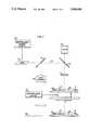
- FIG. 1is a schematic diagram of apparatus for depositing conductors in accordance with an illustrative embodiment of the invention
- FIG. 2is a top view of part of the integrated circuit of FIG. 1 showing how a continuous conductor is defined along the surface of the integrated circuit;
- FIG. 3is a graph of temperature versus time for various velocities of the laser beam on the surface of the integrated circuit of FIG. 1.
- FIG. 1there is shown schematically apparatus for defining a metal conductor on the surface of a semiconductor chip or integrated circuit substrate 11 in accordance with the principals of the present invention.
- the semiconductor substrate 11is intended to represent a semiconductor integrated circuit chip that may have, typically, dimensions of only about one centimeter on a side, while other components in the figure are relatively much larger.
- the purpose of the process illustratedis to make a controllable conductive interconnection between metallic bonding pads 12 and 13, such as gold, on the surface of the substrate 11.
- the inventionis applicable to other devices and other substrates; specifically, it is admirably suited to the need for repairing conductors on the surface of AVP substrates, including such AVP substrates as may be coated with polyimide.
- White light reflected back through objective 17passes through second dichroic mirror 16 and is intercepted by a closed circuit television camera 21.
- the image projected to television camera 21is a magnified image of the intersection of path 14 with the surface of the substrate 11.
- the laser 13is connected to a controllable power supply 22 which allows control of the laser power level.
- the substrate surface 11is coated with a metal-organic ink material 25 which may be applied, for example, by spin coating over the entire surface a wafer containing the substrate 11 to a thickness of, for example, approximately two microns.
- the inkmay illustratively be bright gold A3728 screen ink commercially available from Englehard, Inc. of East Newark, N.J. Such ink is formed from gold chloride in solution with a polymer forming compound to form a gold terpene mercaptide. Gold is the principle metallic component and the ink is widely used commercially for making decorative gold films.
- the substratemay be dried for twenty minutes at ninety degrees Centigrade to remove certain volatile, organic solvents from the metals organic ink 25.
- the temperature rise in the inkmust be appropriately gradual, or in other words, the temperature rise must be ramped during deposition onto the substrate just as the laser power is ramped for the initial deposition.
- the speed of the substrate necessary for giving appropriate rampingcan be derived from the general expression for temperature ramping needed to give complete pyrolyzation.
- the temperature T in accordance with the above relationshipsis plotted in FIG. 3 as a function of time in seconds.
- Curve 30is a plot of temperature versus time with a substrate velocity v equal to one micron per second.
- Graph 31shows the change of temperature with a velocity of five microns per second and
- Curve 32shows temperature change with a velocity of fifty microns per second.
- the temperature ramp-up timeshould be between two and five seconds to give complete pyrolysis. One can see from FIG. 3 that this would be obtained by making the scanning rate between one and five microns per second. If it were as much as fifty microns per second, the temperature ramp-up time as shown by Curve 32 would be inadequate; that is, the temperature would be ramped to maximum during a time of much less than two seconds.
- the laser power required for pyrolysis on a highly conductive substrateis about four times that required on a generally insulative substrate.
- the operatorshould control the laser power to be approximately four times as high during the period at which the laser spot impinges the bonding pad 27 as when it impinges the substrate 11. This is best accomplished by having the substrate move in the X direction at a constant speed, beginning to reduce power as the laser spot first touches the substrate 11 and completing the transition to a lower power as the laser spot leaves the bonding pad 12 and is fully focused on the substrate 11. After bonding pad 13 is reached, the laser power is again increased so that metal deposition conditions match those that were obtained during deposition bonding pad 12.
- the resulting conductorwas about one thousand angstroms (0.1 micron) thick with a resistivity of about 8 ⁇ 10 -6 ohm-centimeters. This resistivity is only about four times greater than that of bulk gold, implying a very high gold purity and excellent electrical conductor characteristics.
- Auger and Rutherford back scattering (RBS) analysisrevealed traces of impurities of under 2% of vanadium, sulfur, carbon and oxygen which were not completely volatilized out from the original ink. The film thus, has good electrical properties, and we have found that it adheres well to the metal and silicon dioxide substrates. Reliable continuous conductors ten microns wide and as much as one centimeter long have been made.
- the continuous wave argon laserhad a wave-length of 5145 angstroms.
- the lens 17was a 100 ⁇ objective used to focus the laser light to a spot of about ten microns.
- the laser power usedwas 250 mW and for deposition on the silicon dioxide the laser power was 65 mW.
- bonding pad 12may be taken to represent one of two duplicate circuits and bonding pad 13 as the main circuit of an integrated circuit, in which case the method is one for selectively connecting a "redundant" circuit, to a larger circuit system.
- bonding pads 12 and 13may be considered as opposite portions of an accidentally broken conductor of either an integrated circuit chip or an AVP substrate, in which case the process described is one for repairing the broken conductor.
- the surface of the substrate 11could be coated with polyimide.
Landscapes
- Chemical & Material Sciences (AREA)
- Engineering & Computer Science (AREA)
- Metallurgy (AREA)
- Organic Chemistry (AREA)
- Chemical Kinetics & Catalysis (AREA)
- General Chemical & Material Sciences (AREA)
- Materials Engineering (AREA)
- Mechanical Engineering (AREA)
- Physics & Mathematics (AREA)
- Condensed Matter Physics & Semiconductors (AREA)
- Health & Medical Sciences (AREA)
- Toxicology (AREA)
- General Physics & Mathematics (AREA)
- Manufacturing & Machinery (AREA)
- Computer Hardware Design (AREA)
- Microelectronics & Electronic Packaging (AREA)
- Power Engineering (AREA)
- Thermal Sciences (AREA)
- Internal Circuitry In Semiconductor Integrated Circuit Devices (AREA)
Abstract
Description
Claims (10)
Priority Applications (2)
| Application Number | Priority Date | Filing Date | Title |
|---|---|---|---|
| US07/397,700US5064685A (en) | 1989-08-23 | 1989-08-23 | Electrical conductor deposition method |
| JP2194118AJPH0697662B2 (en) | 1989-08-23 | 1990-07-24 | Conductor deposition method and bonding pad selective interconnection method |
Applications Claiming Priority (1)
| Application Number | Priority Date | Filing Date | Title |
|---|---|---|---|
| US07/397,700US5064685A (en) | 1989-08-23 | 1989-08-23 | Electrical conductor deposition method |
Publications (1)
| Publication Number | Publication Date |
|---|---|
| US5064685Atrue US5064685A (en) | 1991-11-12 |
Family
ID=23572281
Family Applications (1)
| Application Number | Title | Priority Date | Filing Date |
|---|---|---|---|
| US07/397,700Expired - LifetimeUS5064685A (en) | 1989-08-23 | 1989-08-23 | Electrical conductor deposition method |
Country Status (2)
| Country | Link |
|---|---|
| US (1) | US5064685A (en) |
| JP (1) | JPH0697662B2 (en) |
Cited By (29)
| Publication number | Priority date | Publication date | Assignee | Title |
|---|---|---|---|---|
| US5418349A (en)* | 1993-06-04 | 1995-05-23 | Xerox Corporation | Process for reducing thickness of a polymeric photoconductive coating on a photoreceptor with laser |
| US5534312A (en)* | 1994-11-14 | 1996-07-09 | Simon Fraser University | Method for directly depositing metal containing patterned films |
| US5728626A (en)* | 1993-07-26 | 1998-03-17 | At&T Global Information Solutions Company | Spin-on conductor process for integrated circuits |
| GB2337635A (en)* | 1998-05-22 | 1999-11-24 | Boris Aronovich Gurovich | Method of forming a conducting structure on a substrate |
| DE19934089A1 (en)* | 1999-07-19 | 2001-01-25 | Univ Schiller Jena | Raising electrical conductivity in multi-component materials e.g. semiconductors and insulators comprises withdrawing a material component from the starting material by particle radiation |
| US20030124457A1 (en)* | 2001-12-28 | 2003-07-03 | Jung Won Cheol | Organic metal precursor for use in forming metal containing patterned films |
| US6599587B2 (en) | 2001-09-11 | 2003-07-29 | Samsung Eleectronics Co., Ltd. | Organometallic precursor for forming metal pattern and method of forming metal pattern using the same |
| US20030157440A1 (en)* | 2002-01-03 | 2003-08-21 | Byun Young Hun | Process of forming a micro-pattern of a metal or a metal oxide |
| US20030207568A1 (en)* | 2002-04-30 | 2003-11-06 | Byun Young Hun | Organometallic precursor for forming metal pattern and method of forming metal pattern using the same |
| US20040005412A1 (en)* | 2002-07-03 | 2004-01-08 | Byun Young Hun | Organometallic precursor mixture for forming metal alloy pattern and method of forming metal alloy pattern using the same |
| US20040026258A1 (en)* | 2002-06-26 | 2004-02-12 | No Chang Ho | Method for forming high reflective micropattern |
| US6777036B2 (en) | 2001-06-06 | 2004-08-17 | Simon Fraser University | Method for the deposition of materials from mesomorphous films |
| US20040197493A1 (en)* | 1998-09-30 | 2004-10-07 | Optomec Design Company | Apparatus, methods and precision spray processes for direct write and maskless mesoscale material deposition |
| US20050046664A1 (en)* | 1998-09-30 | 2005-03-03 | Optomec Design Company | Direct writeTM system |
| US20050084689A1 (en)* | 2003-06-30 | 2005-04-21 | Hwang Euk C. | Organometallic precursor composition and method of forming metal film or pattern using the same |
| US20050156991A1 (en)* | 1998-09-30 | 2005-07-21 | Optomec Design Company | Maskless direct write of copper using an annular aerosol jet |
| US20050250051A1 (en)* | 2002-11-25 | 2005-11-10 | Kim Jin Y | Organometallic composition for forming a metal alloy pattern and a method of forming such a pattern using the composition |
| US7485345B2 (en) | 1998-09-30 | 2009-02-03 | Optomec Design Company | Apparatuses and methods for maskless mesoscale material deposition |
| US7674671B2 (en) | 2004-12-13 | 2010-03-09 | Optomec Design Company | Aerodynamic jetting of aerosolized fluids for fabrication of passive structures |
| EP1724121A4 (en)* | 2004-02-02 | 2010-05-19 | Sergei Nicolaevich Maximovsky | Method for producing a metallised image on a sheet material and device for carrying out said method |
| WO2010128107A1 (en)* | 2009-05-07 | 2010-11-11 | Neodec B.V. | Process for manufacturing conductive tracks |
| US7938341B2 (en) | 2004-12-13 | 2011-05-10 | Optomec Design Company | Miniature aerosol jet and aerosol jet array |
| US8110247B2 (en) | 1998-09-30 | 2012-02-07 | Optomec Design Company | Laser processing for heat-sensitive mesoscale deposition of oxygen-sensitive materials |
| US8272579B2 (en) | 2007-08-30 | 2012-09-25 | Optomec, Inc. | Mechanically integrated and closely coupled print head and mist source |
| US8887658B2 (en) | 2007-10-09 | 2014-11-18 | Optomec, Inc. | Multiple sheath multiple capillary aerosol jet |
| US9192054B2 (en) | 2007-08-31 | 2015-11-17 | Optomec, Inc. | Apparatus for anisotropic focusing |
| US10632746B2 (en) | 2017-11-13 | 2020-04-28 | Optomec, Inc. | Shuttering of aerosol streams |
| US10994473B2 (en) | 2015-02-10 | 2021-05-04 | Optomec, Inc. | Fabrication of three dimensional structures by in-flight curing of aerosols |
| US12172444B2 (en) | 2021-04-29 | 2024-12-24 | Optomec, Inc. | High reliability sheathed transport path for aerosol jet devices |
Families Citing this family (1)
| Publication number | Priority date | Publication date | Assignee | Title |
|---|---|---|---|---|
| JP2021190454A (en)* | 2020-05-26 | 2021-12-13 | ローム株式会社 | Semiconductor devices and methods for manufacturing semiconductor devices |
Citations (11)
| Publication number | Priority date | Publication date | Assignee | Title |
|---|---|---|---|---|
| US4239789A (en)* | 1979-05-08 | 1980-12-16 | International Business Machines Corporation | Maskless method for electroless plating patterns |
| US4340654A (en)* | 1980-06-19 | 1982-07-20 | Campi James G | Defect-free photomask |
| US4340617A (en)* | 1980-05-19 | 1982-07-20 | Massachusetts Institute Of Technology | Method and apparatus for depositing a material on a surface |
| US4444801A (en)* | 1981-01-14 | 1984-04-24 | Hitachi, Ltd. | Method and apparatus for correcting transparent defects on a photomask |
| US4511597A (en)* | 1983-10-12 | 1985-04-16 | Kollmorgen Technologies Corporation | Method for depositing a metal on a surface |
| US4526807A (en)* | 1984-04-27 | 1985-07-02 | General Electric Company | Method for deposition of elemental metals and metalloids on substrates |
| US4636403A (en)* | 1985-04-29 | 1987-01-13 | At&T Technologies, Inc. | Method of repairing a defective photomask |
| US4933204A (en)* | 1988-09-23 | 1990-06-12 | Rockwell International Corporation | Method of producing a gold film |
| US4957880A (en)* | 1985-05-29 | 1990-09-18 | Kabushiki Kaisha Toshiba | Method for producing semiconductor device including a refractory metal pattern |
| US4957775A (en)* | 1986-05-29 | 1990-09-18 | Massachusetts Institute Of Technology | Method and apparatus for refractory metal deposition |
| US4960613A (en)* | 1988-10-04 | 1990-10-02 | General Electric Company | Laser interconnect process |
Family Cites Families (2)
| Publication number | Priority date | Publication date | Assignee | Title |
|---|---|---|---|---|
| JPS61244048A (en)* | 1985-04-23 | 1986-10-30 | Matsushita Electric Ind Co Ltd | Multilayer wiring formation method |
| JPH0748496B2 (en)* | 1986-11-20 | 1995-05-24 | 日本電気株式会社 | Laser-based wiring formation method |
- 1989
- 1989-08-23USUS07/397,700patent/US5064685A/ennot_activeExpired - Lifetime
- 1990
- 1990-07-24JPJP2194118Apatent/JPH0697662B2/ennot_activeExpired - Lifetime
Patent Citations (11)
| Publication number | Priority date | Publication date | Assignee | Title |
|---|---|---|---|---|
| US4239789A (en)* | 1979-05-08 | 1980-12-16 | International Business Machines Corporation | Maskless method for electroless plating patterns |
| US4340617A (en)* | 1980-05-19 | 1982-07-20 | Massachusetts Institute Of Technology | Method and apparatus for depositing a material on a surface |
| US4340654A (en)* | 1980-06-19 | 1982-07-20 | Campi James G | Defect-free photomask |
| US4444801A (en)* | 1981-01-14 | 1984-04-24 | Hitachi, Ltd. | Method and apparatus for correcting transparent defects on a photomask |
| US4511597A (en)* | 1983-10-12 | 1985-04-16 | Kollmorgen Technologies Corporation | Method for depositing a metal on a surface |
| US4526807A (en)* | 1984-04-27 | 1985-07-02 | General Electric Company | Method for deposition of elemental metals and metalloids on substrates |
| US4636403A (en)* | 1985-04-29 | 1987-01-13 | At&T Technologies, Inc. | Method of repairing a defective photomask |
| US4957880A (en)* | 1985-05-29 | 1990-09-18 | Kabushiki Kaisha Toshiba | Method for producing semiconductor device including a refractory metal pattern |
| US4957775A (en)* | 1986-05-29 | 1990-09-18 | Massachusetts Institute Of Technology | Method and apparatus for refractory metal deposition |
| US4933204A (en)* | 1988-09-23 | 1990-06-12 | Rockwell International Corporation | Method of producing a gold film |
| US4960613A (en)* | 1988-10-04 | 1990-10-02 | General Electric Company | Laser interconnect process |
Non-Patent Citations (2)
| Title |
|---|
| Ralph T. Hopper, "How to apply noble metals to ceramics," Ceramic Industry Magazine, 06/63, pp. 65-76. |
| Ralph T. Hopper, How to apply noble metals to ceramics, Ceramic Industry Magazine , 06/63, pp. 65 76.* |
Cited By (49)
| Publication number | Priority date | Publication date | Assignee | Title |
|---|---|---|---|---|
| US5418349A (en)* | 1993-06-04 | 1995-05-23 | Xerox Corporation | Process for reducing thickness of a polymeric photoconductive coating on a photoreceptor with laser |
| US5728626A (en)* | 1993-07-26 | 1998-03-17 | At&T Global Information Solutions Company | Spin-on conductor process for integrated circuits |
| US5534312A (en)* | 1994-11-14 | 1996-07-09 | Simon Fraser University | Method for directly depositing metal containing patterned films |
| GB2337635B (en)* | 1998-05-22 | 2003-03-26 | Boris Aronovich Gurovich | Method of forming a conducting structure |
| GB2337635A (en)* | 1998-05-22 | 1999-11-24 | Boris Aronovich Gurovich | Method of forming a conducting structure on a substrate |
| US7270844B2 (en) | 1998-09-30 | 2007-09-18 | Optomec Design Company | Direct write™ system |
| US7987813B2 (en) | 1998-09-30 | 2011-08-02 | Optomec, Inc. | Apparatuses and methods for maskless mesoscale material deposition |
| US8110247B2 (en) | 1998-09-30 | 2012-02-07 | Optomec Design Company | Laser processing for heat-sensitive mesoscale deposition of oxygen-sensitive materials |
| US8455051B2 (en) | 1998-09-30 | 2013-06-04 | Optomec, Inc. | Apparatuses and methods for maskless mesoscale material deposition |
| US7658163B2 (en) | 1998-09-30 | 2010-02-09 | Optomec Design Company | Direct write# system |
| US7485345B2 (en) | 1998-09-30 | 2009-02-03 | Optomec Design Company | Apparatuses and methods for maskless mesoscale material deposition |
| US20050156991A1 (en)* | 1998-09-30 | 2005-07-21 | Optomec Design Company | Maskless direct write of copper using an annular aerosol jet |
| US20040197493A1 (en)* | 1998-09-30 | 2004-10-07 | Optomec Design Company | Apparatus, methods and precision spray processes for direct write and maskless mesoscale material deposition |
| US20050046664A1 (en)* | 1998-09-30 | 2005-03-03 | Optomec Design Company | Direct writeTM system |
| US20050163917A1 (en)* | 1998-09-30 | 2005-07-28 | Optomec Design Company | Direct writeTM system |
| DE19934089A1 (en)* | 1999-07-19 | 2001-01-25 | Univ Schiller Jena | Raising electrical conductivity in multi-component materials e.g. semiconductors and insulators comprises withdrawing a material component from the starting material by particle radiation |
| US6777036B2 (en) | 2001-06-06 | 2004-08-17 | Simon Fraser University | Method for the deposition of materials from mesomorphous films |
| US6599587B2 (en) | 2001-09-11 | 2003-07-29 | Samsung Eleectronics Co., Ltd. | Organometallic precursor for forming metal pattern and method of forming metal pattern using the same |
| US20030124457A1 (en)* | 2001-12-28 | 2003-07-03 | Jung Won Cheol | Organic metal precursor for use in forming metal containing patterned films |
| US6965045B2 (en) | 2001-12-28 | 2005-11-15 | Samsung Electronics Co., Ltd. | Organic metal precursor for use in forming metal containing patterned films |
| US20030157440A1 (en)* | 2002-01-03 | 2003-08-21 | Byun Young Hun | Process of forming a micro-pattern of a metal or a metal oxide |
| US7033738B2 (en) | 2002-01-03 | 2006-04-25 | Samsung Electronics Co., Ltd. | Process of forming a micro-pattern of a metal or a metal oxide |
| US20030207568A1 (en)* | 2002-04-30 | 2003-11-06 | Byun Young Hun | Organometallic precursor for forming metal pattern and method of forming metal pattern using the same |
| US6774034B2 (en) | 2002-04-30 | 2004-08-10 | Samsung Electronics Co., Ltd | Organometallic precursor for forming metal pattern and method of forming metal pattern using the same |
| US20040026258A1 (en)* | 2002-06-26 | 2004-02-12 | No Chang Ho | Method for forming high reflective micropattern |
| US20040005412A1 (en)* | 2002-07-03 | 2004-01-08 | Byun Young Hun | Organometallic precursor mixture for forming metal alloy pattern and method of forming metal alloy pattern using the same |
| US7014979B2 (en) | 2002-07-03 | 2006-03-21 | Samsung Electronics Co., Ltd. | Organometallic precursor mixture for forming metal alloy pattern and method of forming metal alloy pattern using the same |
| US8715914B2 (en) | 2002-11-25 | 2014-05-06 | Samsung Electronics Co., Ltd. | Organometallic composition for forming a metal alloy pattern and a method of forming such a pattern using the composition |
| US20110104617A1 (en)* | 2002-11-25 | 2011-05-05 | Jin Young Kim | Organometallic composition for forming a metal alloy pattern and a method of forming such a pattern using the composition |
| US20050250051A1 (en)* | 2002-11-25 | 2005-11-10 | Kim Jin Y | Organometallic composition for forming a metal alloy pattern and a method of forming such a pattern using the composition |
| US7883838B2 (en) | 2002-11-25 | 2011-02-08 | Samsung Electronics Co., Ltd. | Organometallic composition for forming a metal alloy pattern and a method of forming such a pattern using the composition |
| US7374701B2 (en)* | 2003-06-30 | 2008-05-20 | Samsung Electronics Co., Ltd. | Organometallic precursor composition and method of forming metal film or pattern using the same |
| US20050084689A1 (en)* | 2003-06-30 | 2005-04-21 | Hwang Euk C. | Organometallic precursor composition and method of forming metal film or pattern using the same |
| EP1724121A4 (en)* | 2004-02-02 | 2010-05-19 | Sergei Nicolaevich Maximovsky | Method for producing a metallised image on a sheet material and device for carrying out said method |
| US9607889B2 (en) | 2004-12-13 | 2017-03-28 | Optomec, Inc. | Forming structures using aerosol jet® deposition |
| US7938341B2 (en) | 2004-12-13 | 2011-05-10 | Optomec Design Company | Miniature aerosol jet and aerosol jet array |
| US8132744B2 (en) | 2004-12-13 | 2012-03-13 | Optomec, Inc. | Miniature aerosol jet and aerosol jet array |
| US7674671B2 (en) | 2004-12-13 | 2010-03-09 | Optomec Design Company | Aerodynamic jetting of aerosolized fluids for fabrication of passive structures |
| US8640975B2 (en) | 2004-12-13 | 2014-02-04 | Optomec, Inc. | Miniature aerosol jet and aerosol jet array |
| US8796146B2 (en) | 2004-12-13 | 2014-08-05 | Optomec, Inc. | Aerodynamic jetting of blended aerosolized materials |
| US9114409B2 (en) | 2007-08-30 | 2015-08-25 | Optomec, Inc. | Mechanically integrated and closely coupled print head and mist source |
| US8272579B2 (en) | 2007-08-30 | 2012-09-25 | Optomec, Inc. | Mechanically integrated and closely coupled print head and mist source |
| US9192054B2 (en) | 2007-08-31 | 2015-11-17 | Optomec, Inc. | Apparatus for anisotropic focusing |
| US8887658B2 (en) | 2007-10-09 | 2014-11-18 | Optomec, Inc. | Multiple sheath multiple capillary aerosol jet |
| WO2010128107A1 (en)* | 2009-05-07 | 2010-11-11 | Neodec B.V. | Process for manufacturing conductive tracks |
| US10994473B2 (en) | 2015-02-10 | 2021-05-04 | Optomec, Inc. | Fabrication of three dimensional structures by in-flight curing of aerosols |
| US10632746B2 (en) | 2017-11-13 | 2020-04-28 | Optomec, Inc. | Shuttering of aerosol streams |
| US10850510B2 (en) | 2017-11-13 | 2020-12-01 | Optomec, Inc. | Shuttering of aerosol streams |
| US12172444B2 (en) | 2021-04-29 | 2024-12-24 | Optomec, Inc. | High reliability sheathed transport path for aerosol jet devices |
Also Published As
| Publication number | Publication date |
|---|---|
| JPH0697662B2 (en) | 1994-11-30 |
| JPH0389521A (en) | 1991-04-15 |
Similar Documents
| Publication | Publication Date | Title |
|---|---|---|
| US5064685A (en) | Electrical conductor deposition method | |
| US4931323A (en) | Thick film copper conductor patterning by laser | |
| US4714516A (en) | Method to produce via holes in polymer dielectrics for multiple electronic circuit chip packaging | |
| US4764485A (en) | Method for producing via holes in polymer dielectrics | |
| US4636403A (en) | Method of repairing a defective photomask | |
| US3768157A (en) | Process of manufacture of semiconductor product | |
| US5832595A (en) | Method of modifying conductive lines of an electronic circuit board and its apparatus | |
| JP3398376B2 (en) | Method of manufacturing via hole in polymer dielectric layer | |
| US4273859A (en) | Method of forming solder bump terminals on semiconductor elements | |
| US5459098A (en) | Maskless laser writing of microscopic metallic interconnects | |
| EP0165685A2 (en) | Laser-based system for the total repair of photomasks | |
| US4704304A (en) | Method for repair of opens in thin film lines on a substrate | |
| US5026664A (en) | Method of providing a semiconductor IC device with an additional conduction path | |
| US5246745A (en) | Laser-induced chemical vapor deposition of thin-film conductors | |
| US4284659A (en) | Insulation layer reflow | |
| US5124175A (en) | Method of patterned metal reflow on interconnect substrates | |
| US4580030A (en) | Thick film resistor, method of trimming thick film resistor, and printed circuit board having thick film resistor | |
| US5230970A (en) | Method of forming metal regions | |
| JP2594972B2 (en) | Wiring forming method and apparatus | |
| JPH03215941A (en) | Semiconductor device, insulating film forming method and device | |
| US4827610A (en) | Method of creating solder or brazing barriers | |
| JP3009157B2 (en) | Method and apparatus for forming wiring film | |
| JP2655666B2 (en) | Wiring formation method | |
| JP3149526B2 (en) | Wiring formation method | |
| JP3111615B2 (en) | Method and apparatus for forming transparent film |
Legal Events
| Date | Code | Title | Description |
|---|---|---|---|
| AS | Assignment | Owner name:AMERICAN TELEPHONE AND TELEGRAPH COMPANY, NEW YORK Free format text:ASSIGNMENT OF ASSIGNORS INTEREST.;ASSIGNORS:KESTENBAUM, AMI;SERAFINO, ANTHONY J.;REEL/FRAME:005116/0475 Effective date:19890818 Owner name:BELL TELEPHONE LABORATORIES, INCORPORATED, NEW JER Free format text:ASSIGNMENT OF ASSIGNORS INTEREST.;ASSIGNORS:KESTENBAUM, AMI;SERAFINO, ANTHONY J.;REEL/FRAME:005116/0475 Effective date:19890818 | |
| STCF | Information on status: patent grant | Free format text:PATENTED CASE | |
| FEPP | Fee payment procedure | Free format text:PAYOR NUMBER ASSIGNED (ORIGINAL EVENT CODE: ASPN); ENTITY STATUS OF PATENT OWNER: LARGE ENTITY | |
| FPAY | Fee payment | Year of fee payment:4 | |
| FEPP | Fee payment procedure | Free format text:PAYER NUMBER DE-ASSIGNED (ORIGINAL EVENT CODE: RMPN); ENTITY STATUS OF PATENT OWNER: LARGE ENTITY Free format text:PAYOR NUMBER ASSIGNED (ORIGINAL EVENT CODE: ASPN); ENTITY STATUS OF PATENT OWNER: LARGE ENTITY | |
| FPAY | Fee payment | Year of fee payment:8 | |
| FEPP | Fee payment procedure | Free format text:PAYOR NUMBER ASSIGNED (ORIGINAL EVENT CODE: ASPN); ENTITY STATUS OF PATENT OWNER: LARGE ENTITY Free format text:PAYER NUMBER DE-ASSIGNED (ORIGINAL EVENT CODE: RMPN); ENTITY STATUS OF PATENT OWNER: LARGE ENTITY | |
| FPAY | Fee payment | Year of fee payment:12 |