US5063429A - High density input/output cell arrangement for integrated circuits - Google Patents
High density input/output cell arrangement for integrated circuitsDownload PDFInfo
- Publication number
- US5063429A US5063429AUS07/583,754US58375490AUS5063429AUS 5063429 AUS5063429 AUS 5063429AUS 58375490 AUS58375490 AUS 58375490AUS 5063429 AUS5063429 AUS 5063429A
- Authority
- US
- United States
- Prior art keywords
- input
- pad
- output cell
- output
- power bus
- Prior art date
- Legal status (The legal status is an assumption and is not a legal conclusion. Google has not performed a legal analysis and makes no representation as to the accuracy of the status listed.)
- Expired - Lifetime
Links
Images


Classifications
- H—ELECTRICITY
- H10—SEMICONDUCTOR DEVICES; ELECTRIC SOLID-STATE DEVICES NOT OTHERWISE PROVIDED FOR
- H10D—INORGANIC ELECTRIC SEMICONDUCTOR DEVICES
- H10D84/00—Integrated devices formed in or on semiconductor substrates that comprise only semiconducting layers, e.g. on Si wafers or on GaAs-on-Si wafers
- H10D84/90—Masterslice integrated circuits
- H10D84/998—Input and output buffer/driver structures
Definitions
- the present inventionrelates to integrated circuit products. More particularly, the invention is directed to an arrangement of input/output cells for application specific integrated circuits (ASICs).
- ASICsapplication specific integrated circuits
- LSIlarge scale integrated
- VLSIvery large scale integrated
- the arrangement of the input/output cells around the peripheryis a separate design task, i.e. input/output cells are arranged more or less independently from the arrangement of arrays of gates or standard cells in the interior of the integrated circuit.
- LSI and VLSI circuitstypically can provide more logic functions from interior gates and/or cells
- many input/output designs for LSI and VLSI circuitsare known as pad limited designs.
- a pad limited designoccurs when the number of input and output pads, and their associated input/output cells, which can be spaced around the periphery of an integrated circuit is a limiting design factor.
- the methodology used for a pad limited designis straight forward. First, the number of pads (with their associated input/output cells) that the periphery is required to have, is selected. Next, the perimeter of the input/output pad region is determined from the size of the integrated circuit substrate. Given these parameters, a circuit layout program automatically spaces the input/output pads and cells equally around the periphery. The automatic layout program allots the same space to each input/output pad, and any unused space is equally distributed between pads by the layout program.
- the former patented inventionprevents latch-up by extra fabrication steps (which take extra material) to inhibit the formation of the parasitic devices that cause the latch-up phenomenon, and the latter patented invention arranges its I/O cells perpendicularly so that the gain of any parasitic device is lowered.
- the lower gainlowers the sensitivity of the parasitic device to noise triggering.
- the latter patentlowers the gain by physically spacing the input/output cells (and thereby waste chip space) in order to reduce the possibility of a parasitic devices that may latch-up.
- an object of the present inventionto provide a method and arrangement of input/output cells for non-pad limited designs that do not waste space in the input/output pad region.
- an input/output cell arrangement on an integrated circuit substrateincluding a two level outer power bus around the periphery of said integrated circuit substrate, and a two layer inner power bus located within the outer two level power bus and encompassing an inner portion of the integrated circuit substrate.
- a plurality of pads for connection of external leadsare located between the outer two level power bus and the inner two level power bus.
- a plurality of input/output cells, each of which is connected to a respective pad,is also located between the outer two level power bus and the inner two level power bus.
- the foregoing objectsare achieved by providing a method of arranging input/output cells including the steps of defining an array space for a plurality input/output cells and their respective pads between an outer power bus and an inner power bus, locating a p-channel transistor portion of each input/output cell between its pad and a first adjacent pad in the array space having one side thereof lying along a first side of its pad, locating a n-channel transistor portion of each input/output cell between its pad and a second adjacent pad in the array space having one side thereof lying along an opposite side of its pad, and alternating the order of occurrence of the n-channel transistor portions and the p-channel transistor portions of input/output cells within the array space such that each p-channel portion is located adjacent to a p-channel portion of an adjacent cell and each n-channel portion is located adjacent to an n-channel portion of an adjacent cell.
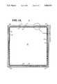
- FIG. 1Ais a plan view of an integrated circuit substrate, according to the present invention.
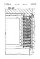
- FIG. 1Bis an enlarged view of the encircled portion of FIG. 1A;
- FIGS. 2A and 2Bwhen joined along the dotted line, provide a plan view of a single input/output pad and its related circuitry, according to the present invention.
- FIG. 3is partial cross section view along line 3--3 in FIG. 1B, showing an P+ conductive region diffused in the substrate.
- CMOS integrated circuit 10in accordance with the present invention.
- the integrated circuit 10 in the shown embodimentis for an n-well process device, but a p-well process device is also contemplated, and is considered to be within the scope of the present invention.
- the integrated circuit 10has a substrate 11 having an arrangement of CMOS input/output pad circuits 12.
- the substrate 11has a two level power bus 14 around its outer perimeter such that the power bus 14 is located between the edges of the substrate 11 and the outer edges of the input/output pad circuits 12. Since the integrated circuit 10 is made by an n-well process, this substrate 11 will be p-silicon.
- the input/output pad circuits 12provide connections between the internal logic circuits (not shown) of the integrated circuit 10 and external integrated circuits and/or similar devices (not shown).
- the two level power bus 14preferably is arranged with a conductor carrying the drain voltage VDD on an upper level and a conductor carrying the source voltage VSS on a lower level, as will be explained in greater detail later.
- a second two level power bus 16is located between the inner edges of the input/output pad circuits 12 and internal logic circuits (not shown) located within the inner portion 22 of the integrated circuit 10.
- the second two level power bus 16is arranged in the same fashion as the first two level power bus 14 with the conductor carrying VDD on an upper level and the conductor carrying VSS on a lower level. This arrangement places the bus that is usually connected to ground nearest to the substrate. For other processes, that bus closest to the substrate 11 may be the drain bus instead of the source bus of the embodiment shown in FIG. 1, and such modifications are considered to be within the scope of the present invention.
- the input/output pad circuits 12each have a metal pad area 18, where electrical contact is made with a respective lead (not shown).
- each left oriented type 12Lhas a polysilicon conductor 20 running from a left side of its pad 18 under the inner two level power bus 16 in order to provide an input connection to internal logic circuits within the inner portion 22.
- the left oriented type 12Lhas a bank 28 of N-channel field effect transistors (N-FETs) located to the left of the pad 18, as shown in FIG. 1B, and a bank 30 of P-channel field effect transistors (P-FETs) located to the right thereof.
- N-FETsN-channel field effect transistors
- P-FETsP-channel field effect transistors
- Each of the N-FETs in bank 28has its gate connected to a common input (as will be described in conjunction with FIGS. 2A and 2B).
- each of the P-FETs in bank 30has its gate connected to a second common input.
- the common input of the bank 28is connected to a polysilicon conductor 24, which runs from the left corner, as viewed from the inner portion 22 of the integrated circuit 10, of the left oriented type 12L of input/output pad under the inner two level bus 16 to the inner portion 22.
- the common input of bank 30is connected to another polysilicon conductor 26 which runs from the right corner, as viewed from the inner portion 22 of the integrated circuit 10, of the left oriented type 12L under the inner two level bus 16 to the inner portion 22.
- Each right oriented type 12R of the input/output pad circuits 12is a mirror image of each left oriented type 12L.
- the bank 28 of N-FETsis located on the right side of the pad 18 of the right oriented type 12R, when viewed from the inner portion 22 as shown in FIG. 1B.
- the bank 30 of P-FETsis located on the left side of the pad 18 of the right oriented type 12R.
- the corners 34 of the integrated circuit 10may be used as inactive guard region such that a bank 28, 30 of FETs adjoining one side of a corner 34 may be either of the same channel polarity or a different channel polarity as that of a second bank 28, 30 of FETs adjoining the opposite edge of the corner 34, without increasing the tendency of the input/output pads 12 to latchup. If space does not permit such large guard bands, the banks 28, 30 of FETs are arranged such that each bank 28, 30 is always adjacent to a similar polarity bank of FETs, even at the corners 34.
- FIGS. 2A and 2Ba plan view of a partially broken away portion of the integrated circuit 10 is described.
- This portion of the integrated circuit 10shows a single left oriented type 12L of the input/output pad circuits 12 with its immediately surrounding circuitry.
- Those skilled in the artwill be able to construct a mirror image right oriented type 12R from the description of the left oriented type 12L and its illustration in FIGS. 2A and 2B.
- the outer two level power bus 14has a first metallization layer 40 located on a first level on top of the substrate 11.
- the outer first metallization layer 40is covered by an insulating layer 41.
- a second metallization layer 42is located on a higher level on top of the insulation layer 41.
- the inner two level power bus 16similarly has an inner first metallization layer 44 on a first level thereof.
- the inner first metallization layer 44is located next to the substrate 11 except in the regions traversed by the polysilicon conductors 20, 24, and 26.
- the regions traversed by the polysilicon conductors 20, 24, and 26,are next to the substrate 11 and a layer of insulation (not shown) is located over the polysilicon conductors 20, 24, and 26 in a manner familiar to those skilled in the art.
- the inner first metallization layer 44is located upon the layer of insulation over the polysilicon conductors 20, 24, and 26.
- the inner first metallization layer 44is covered by an insulting layer 45.
- An inner second metallization layer 46is located on a second level thereof on top of the insulation layer 45.
- the first outer metallization layer 40 and the first inner metallization layer 44may be performed as parts of the same metallization process.
- the pad 18is formed from a first metallization layer 48 upon the substrate 11, covered by an insulation layer (not shown) with numerous vias (not shown) therein, and further covered by a second metallization layer 49, which is laid directly on top of the insulation layer and connected by the numerous vias to the first layer 48.
- the second layer 49is slightly smaller that the first layer 48 and, therefore, part of the first layer 48 is not covered by the second layer 49.
- the pad 18is connected to a via region 50 at the inner left corner of the first layer 48. If the pad 18 is an input pad, a connection is made in the via region 50 from the first layer 48 down to the polysilicon conductor 20. In such a case, signals inputted to the pad 18 are conducted through the via region 50 to the polysilicon conductor 20. The polysilicon conductor transports these signals under the inner two level bus 16 to a logic circuit input (not shown) located in the inner portion 22. Since the banks 28, 30 of FETs are not typically used to provide drive for the input signal to an input pad, the banks 28, 30 typically are connected as electrostatic discharge protection diodes, such connection will be described below. If, on the other hand, the pad 18 is an output pad, then a connection in the via region 50 from the first layer 48 to the polysilicon conductor 20 is not made (although a connection for monitoring or similar function could be made if desired).
- the banks 28 and 30, as previously mentioned,are made up of a plurality of N-FETs and a plurality of P-FETs respectively.
- the bank 28has a first group 60 of N-FETs 61. Only four N-FETs 61 are shown, but the number may be increased to eight or more if a higher current drive is need.
- Each N-FET 61has a gate 62 that is oval in shape. All of the gates 62 are connected to a common point 65 which controls all of the N-FETs 61 in parallel.
- VSSis supplied from outer first metallization layer 40 by two rows of vias 43 up to a second metallization layer 43A which overlays the bank 28.
- the drains 64 of the N-FETs 61are all connected in parallel to the first layer 48 of the pad 18. Thus, all the gates 62, the sources 63, and the drains 64 are respectively connected in parallel and, therefore, the N-FETs 61 operate as a single large N-FET device.
- the bank 28has a second group 52 of N-FETs 53.
- the N-FETs 53have gates 54, sources 56, and drains 57 respectively connected in a manner similar to the N-FETs 60.
- the gates 54are connected to a common conductor 55.
- the sources 56are connected to the VSS first metallization layer 40 through second metallization layer conductor 40A.
- the drains 57are connected to the first metallization layer 48 of the pad 18.
- the N-FETs 53have their gates 54 connected to their sources 56. Connected thus, the FETs 53 operate as a single, large electrostatic discharge protection diode.
- a connection 66is made between the common conductor 65 and the common conductor 55.
- a connectionis provided from common conductor 65 to polysilicon conductor 24 through a via region 68.
- the opposite side of the pad 18, as shown in FIG. 2B,has the bank 30.
- the bank 30has a first group 80 of P-FETs 81. Only four P-FETs 81 are shown, but the number may be increased to eight or more if a higher current drive is need.
- Each P-FET 81has a gate 82 that is oval in shape. All of the gates 82 are connected to a common point 85 which controls all of the P-FETs 81 in parallel.
- VDDis supplied from the outer second metallization layer 42 by a direct connection with a conductor 42A which is also on the second layer of metallization overlaying the bank 30.
- Each of the sources 83is connected by a via to conductor 42A and to second metallization layer conductor 42 carrying VDD.
- the drains 84 of the P-FETs 81are all connected in parallel to the first layer 48 of the pad 18.
- all the gates 82, the sources 83, and the drains 84are respectively connected in parallel and, therefore, all of the P-FETs 81 operate as a single large P-FET device.
- the bank 30has a second group 72 of P-FETs 73.
- the P-FETs 73have gates 74, sources 76, and drains 77 respectively connected in a manner similar to the P-FETs 81.
- the gates 74are connected to a common conductor 75.
- the sources 76are connected to VDD and the outer second layer 42 by the overlying conductor 42A on the second metallization layer.
- the drains 77are connected to the first metallization layer 48 of the pad 18.
- the P-FETs 73have their gates 74 connected to their sources 76. Connected thus, the P-FETs 73 operate as a single large electrostatic discharge protection diode.
- a connection 86is made between the common conductor 85 and the common conductor 75. Conversely, if the pad 18 is an output pad, a connection from common conductor 85 to polysilicon conductor 26 is made through a via region 88. With these connections made, a signal from an inner logic circuit output will be conducted under the inner two level bus 16 to the P-FETs 81, which will sink current delivered to the pad 18 at the desired rate. P-FETs 73 provide electrostatic discharge protection for the input/output pads 12.
- via region 68may be connected to via region 88 by a metallization layer path (not shown) connecting polysilicon conductors 24 and 26 as parallel paths.
- a pull-up resistor 90is needed for a particular interface requirement, one or more may be substituted for a FET as shown.
- any type of input or output pad circuitmay be formed. Because of the shielding on both sides by two level power buses and because of the arranging each pad 12L adjacent to a mirror image pad 12R, the input/output pads 12 are nearly immune to latch up. This input/output pad array design and layout may be performed manually, or the arrangement may be added to a computer aided design program and performed automatically.
- the integrated circuit 10has a P+ conductive region 92 diffused in the upper portion of the substrate 11.
- the conductive region 92is overlaid by an insulating layer 94 of silicon dioxide.
- the silicon dioxide layer 94has a number of vias 96.
- the inner first metallization layer 44overlays the silicon dioxide layer 94 and penetrates through the vias 96 in order to make electrical contact with the conductive region 92.
- the rest of the inner two level power bus 16is located above its first metallization layer 44.
- the P+ region 92assists the first metallization layer 44 in absorbing and dissipating voltage spikes and current surges before they reach the logic circuits located in the inner region 22, where they might trigger a latch up.
- the combination of the arrangements of the banks 28, 30 (shown in FIG. 1A); the location of the outer and inner two level power buses 14, 16 (shown in FIG. 1A); and the P+ conducting region 92eliminates latch up from all but the worst of the voltage spikes and current surges.
Landscapes
- Design And Manufacture Of Integrated Circuits (AREA)
- Semiconductor Integrated Circuits (AREA)
Abstract
Description
Claims (8)
Priority Applications (1)
| Application Number | Priority Date | Filing Date | Title |
|---|---|---|---|
| US07/583,754US5063429A (en) | 1990-09-17 | 1990-09-17 | High density input/output cell arrangement for integrated circuits |
Applications Claiming Priority (1)
| Application Number | Priority Date | Filing Date | Title |
|---|---|---|---|
| US07/583,754US5063429A (en) | 1990-09-17 | 1990-09-17 | High density input/output cell arrangement for integrated circuits |
Publications (1)
| Publication Number | Publication Date |
|---|---|
| US5063429Atrue US5063429A (en) | 1991-11-05 |
Family
ID=24334427
Family Applications (1)
| Application Number | Title | Priority Date | Filing Date |
|---|---|---|---|
| US07/583,754Expired - LifetimeUS5063429A (en) | 1990-09-17 | 1990-09-17 | High density input/output cell arrangement for integrated circuits |
Country Status (1)
| Country | Link |
|---|---|
| US (1) | US5063429A (en) |
Cited By (16)
| Publication number | Priority date | Publication date | Assignee | Title |
|---|---|---|---|---|
| US5341018A (en)* | 1991-09-18 | 1994-08-23 | Nec Corporation | Semiconductor integrated circuit device having a plurality of input circuits each including differently sized transistors |
| US5404035A (en)* | 1992-06-11 | 1995-04-04 | Mitsubishi Denki Kabushiki Kaisha | Multi-voltage-level master-slice integrated circuit |
| US5440153A (en)* | 1994-04-01 | 1995-08-08 | United Technologies Corporation | Array architecture with enhanced routing for linear asics |
| US5581279A (en)* | 1991-12-23 | 1996-12-03 | Cirrus Logic, Inc. | VGA controller circuitry |
| US5691218A (en)* | 1993-07-01 | 1997-11-25 | Lsi Logic Corporation | Method of fabricating a programmable polysilicon gate array base cell structure |
| US5698873A (en)* | 1996-03-08 | 1997-12-16 | Lsi Logic Corporation | High density gate array base cell architecture |
| US5760428A (en)* | 1996-01-25 | 1998-06-02 | Lsi Logic Corporation | Variable width low profile gate array input/output architecture |
| US5777354A (en)* | 1994-09-16 | 1998-07-07 | Lsi Logic Corporation | Low profile variable width input/output cells |
| US6028341A (en)* | 1998-03-09 | 2000-02-22 | United Microelectronics Corp. | Latch up protection and yield improvement device for IC array |
| US6078068A (en)* | 1998-07-15 | 2000-06-20 | Adaptec, Inc. | Electrostatic discharge protection bus/die edge seal |
| US6114731A (en)* | 1998-03-27 | 2000-09-05 | Adaptec, Inc. | Low capacitance ESD structure having a source inside a well and the bottom portion of the drain inside a substrate |
| US6242814B1 (en)* | 1998-07-31 | 2001-06-05 | Lsi Logic Corporation | Universal I/O pad structure for in-line or staggered wire bonding or arrayed flip-chip assembly |
| US6550047B1 (en)* | 2000-10-02 | 2003-04-15 | Artisan Components, Inc. | Semiconductor chip input/output cell design and automated generation methods |
| US6725439B1 (en) | 1998-01-29 | 2004-04-20 | International Business Machines Corporation | Method of automated design and checking for ESD robustness |
| US20040150007A1 (en)* | 2002-12-25 | 2004-08-05 | Matsushita Electric Industrial Co., Ltd. | Semiconductor integrated circuit device |
| US6848089B2 (en)* | 2002-07-31 | 2005-01-25 | International Business Machines Corporation | Method and apparatus for detecting devices that can latchup |
Citations (10)
| Publication number | Priority date | Publication date | Assignee | Title |
|---|---|---|---|---|
| US4511914A (en)* | 1982-07-01 | 1985-04-16 | Motorola, Inc. | Power bus routing for providing noise isolation in gate arrays |
| US4591894A (en)* | 1982-01-20 | 1986-05-27 | Tokyo Shibaura Denki Kabushiki Kaisha | Semiconductor device having a plurality of CMOS I/O cells located at the periphery of the chip arranged in a direction perpendicular to the sides of the chip |
| US4611236A (en)* | 1983-07-09 | 1986-09-09 | Fujitsu Limited | Masterslice semiconductor device |
| US4654689A (en)* | 1984-03-14 | 1987-03-31 | Nec Corporation | Structure of power supply wirings in semiconductor integrated circuit |
| US4660067A (en)* | 1984-07-30 | 1987-04-21 | Nec Corporation | Complementary MOS integrated circuit having means for preventing latch-up phenomenon |
| US4661815A (en)* | 1984-10-03 | 1987-04-28 | Fujitsu Limited | Gate array integrated device having mixed single column type and matrix type arrays |
| US4733288A (en)* | 1982-06-30 | 1988-03-22 | Fujitsu Limited | Gate-array chip |
| US4771327A (en)* | 1986-06-19 | 1988-09-13 | Nec Corporation | Master-slice integrated circuit having an improved arrangement of transistor elements for simplified wirings |
| US4819047A (en)* | 1987-05-15 | 1989-04-04 | Advanced Micro Devices, Inc. | Protection system for CMOS integrated circuits |
| US4924290A (en)* | 1987-08-31 | 1990-05-08 | Kabushiki Kaisha Toshiba | Semiconductor device having improved multilayered wirings |
- 1990
- 1990-09-17USUS07/583,754patent/US5063429A/ennot_activeExpired - Lifetime
Patent Citations (10)
| Publication number | Priority date | Publication date | Assignee | Title |
|---|---|---|---|---|
| US4591894A (en)* | 1982-01-20 | 1986-05-27 | Tokyo Shibaura Denki Kabushiki Kaisha | Semiconductor device having a plurality of CMOS I/O cells located at the periphery of the chip arranged in a direction perpendicular to the sides of the chip |
| US4733288A (en)* | 1982-06-30 | 1988-03-22 | Fujitsu Limited | Gate-array chip |
| US4511914A (en)* | 1982-07-01 | 1985-04-16 | Motorola, Inc. | Power bus routing for providing noise isolation in gate arrays |
| US4611236A (en)* | 1983-07-09 | 1986-09-09 | Fujitsu Limited | Masterslice semiconductor device |
| US4654689A (en)* | 1984-03-14 | 1987-03-31 | Nec Corporation | Structure of power supply wirings in semiconductor integrated circuit |
| US4660067A (en)* | 1984-07-30 | 1987-04-21 | Nec Corporation | Complementary MOS integrated circuit having means for preventing latch-up phenomenon |
| US4661815A (en)* | 1984-10-03 | 1987-04-28 | Fujitsu Limited | Gate array integrated device having mixed single column type and matrix type arrays |
| US4771327A (en)* | 1986-06-19 | 1988-09-13 | Nec Corporation | Master-slice integrated circuit having an improved arrangement of transistor elements for simplified wirings |
| US4819047A (en)* | 1987-05-15 | 1989-04-04 | Advanced Micro Devices, Inc. | Protection system for CMOS integrated circuits |
| US4924290A (en)* | 1987-08-31 | 1990-05-08 | Kabushiki Kaisha Toshiba | Semiconductor device having improved multilayered wirings |
Cited By (17)
| Publication number | Priority date | Publication date | Assignee | Title |
|---|---|---|---|---|
| US5341018A (en)* | 1991-09-18 | 1994-08-23 | Nec Corporation | Semiconductor integrated circuit device having a plurality of input circuits each including differently sized transistors |
| US5581279A (en)* | 1991-12-23 | 1996-12-03 | Cirrus Logic, Inc. | VGA controller circuitry |
| US5404035A (en)* | 1992-06-11 | 1995-04-04 | Mitsubishi Denki Kabushiki Kaisha | Multi-voltage-level master-slice integrated circuit |
| US5691218A (en)* | 1993-07-01 | 1997-11-25 | Lsi Logic Corporation | Method of fabricating a programmable polysilicon gate array base cell structure |
| US5440153A (en)* | 1994-04-01 | 1995-08-08 | United Technologies Corporation | Array architecture with enhanced routing for linear asics |
| US5777354A (en)* | 1994-09-16 | 1998-07-07 | Lsi Logic Corporation | Low profile variable width input/output cells |
| US5760428A (en)* | 1996-01-25 | 1998-06-02 | Lsi Logic Corporation | Variable width low profile gate array input/output architecture |
| US5698873A (en)* | 1996-03-08 | 1997-12-16 | Lsi Logic Corporation | High density gate array base cell architecture |
| US6725439B1 (en) | 1998-01-29 | 2004-04-20 | International Business Machines Corporation | Method of automated design and checking for ESD robustness |
| US6028341A (en)* | 1998-03-09 | 2000-02-22 | United Microelectronics Corp. | Latch up protection and yield improvement device for IC array |
| US6114731A (en)* | 1998-03-27 | 2000-09-05 | Adaptec, Inc. | Low capacitance ESD structure having a source inside a well and the bottom portion of the drain inside a substrate |
| US6078068A (en)* | 1998-07-15 | 2000-06-20 | Adaptec, Inc. | Electrostatic discharge protection bus/die edge seal |
| US6242814B1 (en)* | 1998-07-31 | 2001-06-05 | Lsi Logic Corporation | Universal I/O pad structure for in-line or staggered wire bonding or arrayed flip-chip assembly |
| US6550047B1 (en)* | 2000-10-02 | 2003-04-15 | Artisan Components, Inc. | Semiconductor chip input/output cell design and automated generation methods |
| US6848089B2 (en)* | 2002-07-31 | 2005-01-25 | International Business Machines Corporation | Method and apparatus for detecting devices that can latchup |
| US20040150007A1 (en)* | 2002-12-25 | 2004-08-05 | Matsushita Electric Industrial Co., Ltd. | Semiconductor integrated circuit device |
| US7491986B2 (en)* | 2002-12-25 | 2009-02-17 | Panasonic Corporation | Semiconductor integrated circuit device |
Similar Documents
| Publication | Publication Date | Title |
|---|---|---|
| US5063429A (en) | High density input/output cell arrangement for integrated circuits | |
| EP0098163B1 (en) | Gate-array chip | |
| KR910001982B1 (en) | Insulated Gate Semicast Integrated Circuit | |
| US5218222A (en) | Output ESD protection circuit | |
| US6359472B2 (en) | Semiconductor integrated circuit and its fabrication method | |
| US6222213B1 (en) | Semiconductor integrated circuit device | |
| EP0360477B1 (en) | Integrated circuit power supply contact | |
| JP3074003B2 (en) | Semiconductor integrated circuit device | |
| US5962899A (en) | Electrostatic discharge protection circuit | |
| KR100197989B1 (en) | Semiconductor device having electrostatic protection circuit | |
| US5023689A (en) | Complementary integrated circuit device equipped with latch-up preventing means | |
| KR100325190B1 (en) | Semiconductor integrated circuit | |
| US5814846A (en) | Cell apparatus and method for use in building complex integrated circuit devices | |
| US5760447A (en) | Semiconductor device having pull-up or pull-down resistance | |
| US5434436A (en) | Master-slice type semiconductor integrated circuit device having multi-power supply voltage | |
| EP0329152B1 (en) | Semiconductor device with gate array | |
| JPH0316164A (en) | Semiconductor device | |
| JP2833291B2 (en) | CMOS type semiconductor integrated circuit device | |
| EP0092176A2 (en) | Basic cell for integrated-circuit gate arrays | |
| US4959708A (en) | MOS integrated circuit with vertical shield | |
| EP0464452B1 (en) | Semiconductor integrated circuit | |
| JP2840239B2 (en) | Master slice type semiconductor device | |
| KR900003258B1 (en) | Lsi circuit | |
| JPS6362904B2 (en) | ||
| JPH01206646A (en) | semiconductor integrated circuit |
Legal Events
| Date | Code | Title | Description |
|---|---|---|---|
| AS | Assignment | Owner name:NCR CORPORATION, A CORP. OF MD., OHIO Free format text:ASSIGNMENT OF ASSIGNORS INTEREST.;ASSIGNOR:CRAFTS, HAROLD S.;REEL/FRAME:005447/0122 Effective date:19900910 | |
| STCF | Information on status: patent grant | Free format text:PATENTED CASE | |
| AS | Assignment | Owner name:HYUNDAI ELECTRONICS AMERICA Free format text:ASSIGNMENT OF ASSIGNORS INTEREST;ASSIGNOR:AT&T GLOBAL INFORMATION SOLUTIONS COMPANY (FORMERLY KNOWN AS NCR CORPORATION);REEL/FRAME:007408/0104 Effective date:19950215 | |
| FPAY | Fee payment | Year of fee payment:4 | |
| AS | Assignment | Owner name:SYMBIOS LOGIC INC., COLORADO Free format text:ASSIGNMENT OF ASSIGNORS INTEREST;ASSIGNOR:HYUNDAI ELECTRONICS AMERICA;REEL/FRAME:007629/0431 Effective date:19950818 | |
| AS | Assignment | Owner name:SYMBIOS, INC ., COLORADO Free format text:CHANGE OF NAME;ASSIGNOR:SYMBIOS LOGIC INC.;REEL/FRAME:009089/0936 Effective date:19971210 | |
| AS | Assignment | Owner name:LEHMAN COMMERCIAL PAPER INC., AS ADMINISTRATIVE AG Free format text:SECURITY AGREEMENT;ASSIGNORS:HYUNDAI ELECTRONICS AMERICA, A CORP. OF CALIFORNIA;SYMBIOS, INC., A CORP. OF DELAWARE;REEL/FRAME:009396/0441 Effective date:19980226 | |
| AS | Assignment | Owner name:HYUNDAI ELECTRONICS AMERICA, CALIFORNIA Free format text:TERMINATION AND LICENSE AGREEMENT;ASSIGNOR:SYMBIOS, INC.;REEL/FRAME:009596/0539 Effective date:19980806 | |
| FPAY | Fee payment | Year of fee payment:8 | |
| FPAY | Fee payment | Year of fee payment:12 | |
| AS | Assignment | Owner name:HYNIX SEMICONDUCTOR AMERICA INC., CALIFORNIA Free format text:CHANGE OF NAME;ASSIGNOR:HYUNDAI ELECTRONICS AMERICA;REEL/FRAME:015246/0599 Effective date:20010412 Owner name:HYNIX SEMICONDUCTOR INC., KOREA, REPUBLIC OF Free format text:ASSIGNMENT OF ASSIGNORS INTEREST;ASSIGNOR:HYNIX SEMICONDUCTOR AMERICA, INC.;REEL/FRAME:015279/0556 Effective date:20040920 | |
| AS | Assignment | Owner name:MAGNACHIP SEMICONDUCTOR, LTD., KOREA, REPUBLIC OF Free format text:ASSIGNMENT OF ASSIGNORS INTEREST;ASSIGNOR:HYNIX SEMICONDUCTOR, INC.;REEL/FRAME:016216/0649 Effective date:20041004 | |
| AS | Assignment | Owner name:U.S. BANK NATIONAL ASSOCIATION, AS COLLATERAL TRUS Free format text:SECURITY INTEREST;ASSIGNOR:MAGNACHIP SEMICONDUCTOR, LTD.;REEL/FRAME:016470/0530 Effective date:20041223 | |
| AS | Assignment | Owner name:SYMBIOS, INC., COLORADO Free format text:RELEASE OF SECURITY INTEREST;ASSIGNOR:LEHMAN COMMERICAL PAPER INC.;REEL/FRAME:016602/0895 Effective date:20050107 Owner name:HYUNDAI ELECTRONICS AMERICA, CALIFORNIA Free format text:RELEASE OF SECURITY INTEREST;ASSIGNOR:LEHMAN COMMERICAL PAPER INC.;REEL/FRAME:016602/0895 Effective date:20050107 | |
| AS | Assignment | Owner name:MAGNACHIP SEMICONDUCTOR LTD.,KOREA, DEMOCRATIC PEO Free format text:RELEASE BY SECURED PARTY;ASSIGNOR:U.S. BANK NATIONAL ASSOCIATION;REEL/FRAME:024563/0807 Effective date:20100527 | |
| AS | Assignment | Owner name:MAGNACHIP SEMICONDUCTOR LTD., KOREA, REPUBLIC OF Free format text:CORRECTIVE ASSIGNMENT TO CORRECT THE RECEIVING PARTY ADDRESS PREVIOUSLY RECORDED AT REEL: 024563 FRAME: 0807. ASSIGNOR(S) HEREBY CONFIRMS THE RELEASE BY SECURED PARTY;ASSIGNOR:US BANK NATIONAL ASSOCIATION;REEL/FRAME:034469/0001 Effective date:20100527 |