US5062916A - Method for the manufacture of electrical membrane panels having circuits on flexible plastic films - Google Patents
Method for the manufacture of electrical membrane panels having circuits on flexible plastic filmsDownload PDFInfo
- Publication number
- US5062916A US5062916AUS07/561,027US56102790AUS5062916AUS 5062916 AUS5062916 AUS 5062916AUS 56102790 AUS56102790 AUS 56102790AUS 5062916 AUS5062916 AUS 5062916A
- Authority
- US
- United States
- Prior art keywords
- web
- circuits
- circuit
- traces
- along
- Prior art date
- Legal status (The legal status is an assumption and is not a legal conclusion. Google has not performed a legal analysis and makes no representation as to the accuracy of the status listed.)
- Expired - Lifetime
Links
Images


Classifications
- H—ELECTRICITY
- H05—ELECTRIC TECHNIQUES NOT OTHERWISE PROVIDED FOR
- H05K—PRINTED CIRCUITS; CASINGS OR CONSTRUCTIONAL DETAILS OF ELECTRIC APPARATUS; MANUFACTURE OF ASSEMBLAGES OF ELECTRICAL COMPONENTS
- H05K3/00—Apparatus or processes for manufacturing printed circuits
- H05K3/0097—Processing two or more printed circuits simultaneously, e.g. made from a common substrate, or temporarily stacked circuit boards
- G—PHYSICS
- G06—COMPUTING OR CALCULATING; COUNTING
- G06F—ELECTRIC DIGITAL DATA PROCESSING
- G06F2203/00—Indexing scheme relating to G06F3/00 - G06F3/048
- G06F2203/041—Indexing scheme relating to G06F3/041 - G06F3/045
- G06F2203/04102—Flexible digitiser, i.e. constructional details for allowing the whole digitising part of a device to be flexed or rolled like a sheet of paper
- G—PHYSICS
- G06—COMPUTING OR CALCULATING; COUNTING
- G06F—ELECTRIC DIGITAL DATA PROCESSING
- G06F2203/00—Indexing scheme relating to G06F3/00 - G06F3/048
- G06F2203/041—Indexing scheme relating to G06F3/041 - G06F3/045
- G06F2203/04103—Manufacturing, i.e. details related to manufacturing processes specially suited for touch sensitive devices
- H—ELECTRICITY
- H05—ELECTRIC TECHNIQUES NOT OTHERWISE PROVIDED FOR
- H05K—PRINTED CIRCUITS; CASINGS OR CONSTRUCTIONAL DETAILS OF ELECTRIC APPARATUS; MANUFACTURE OF ASSEMBLAGES OF ELECTRICAL COMPONENTS
- H05K1/00—Printed circuits
- H05K1/02—Details
- H05K1/0286—Programmable, customizable or modifiable circuits
- H05K1/0287—Programmable, customizable or modifiable circuits having an universal lay-out, e.g. pad or land grid patterns or mesh patterns
- H05K1/0289—Programmable, customizable or modifiable circuits having an universal lay-out, e.g. pad or land grid patterns or mesh patterns having a matrix lay-out, i.e. having selectively interconnectable sets of X-conductors and Y-conductors in different planes
- H—ELECTRICITY
- H05—ELECTRIC TECHNIQUES NOT OTHERWISE PROVIDED FOR
- H05K—PRINTED CIRCUITS; CASINGS OR CONSTRUCTIONAL DETAILS OF ELECTRIC APPARATUS; MANUFACTURE OF ASSEMBLAGES OF ELECTRICAL COMPONENTS
- H05K1/00—Printed circuits
- H05K1/02—Details
- H05K1/03—Use of materials for the substrate
- H05K1/0393—Flexible materials
- H—ELECTRICITY
- H05—ELECTRIC TECHNIQUES NOT OTHERWISE PROVIDED FOR
- H05K—PRINTED CIRCUITS; CASINGS OR CONSTRUCTIONAL DETAILS OF ELECTRIC APPARATUS; MANUFACTURE OF ASSEMBLAGES OF ELECTRICAL COMPONENTS
- H05K1/00—Printed circuits
- H05K1/02—Details
- H05K1/14—Structural association of two or more printed circuits
- H05K1/144—Stacked arrangements of planar printed circuit boards
- H—ELECTRICITY
- H05—ELECTRIC TECHNIQUES NOT OTHERWISE PROVIDED FOR
- H05K—PRINTED CIRCUITS; CASINGS OR CONSTRUCTIONAL DETAILS OF ELECTRIC APPARATUS; MANUFACTURE OF ASSEMBLAGES OF ELECTRICAL COMPONENTS
- H05K2203/00—Indexing scheme relating to apparatus or processes for manufacturing printed circuits covered by H05K3/00
- H05K2203/15—Position of the PCB during processing
- H05K2203/1545—Continuous processing, i.e. involving rolls moving a band-like or solid carrier along a continuous production path
- H—ELECTRICITY
- H05—ELECTRIC TECHNIQUES NOT OTHERWISE PROVIDED FOR
- H05K—PRINTED CIRCUITS; CASINGS OR CONSTRUCTIONAL DETAILS OF ELECTRIC APPARATUS; MANUFACTURE OF ASSEMBLAGES OF ELECTRICAL COMPONENTS
- H05K3/00—Apparatus or processes for manufacturing printed circuits
- H05K3/0008—Apparatus or processes for manufacturing printed circuits for aligning or positioning of tools relative to the circuit board
- Y—GENERAL TAGGING OF NEW TECHNOLOGICAL DEVELOPMENTS; GENERAL TAGGING OF CROSS-SECTIONAL TECHNOLOGIES SPANNING OVER SEVERAL SECTIONS OF THE IPC; TECHNICAL SUBJECTS COVERED BY FORMER USPC CROSS-REFERENCE ART COLLECTIONS [XRACs] AND DIGESTS
- Y10—TECHNICAL SUBJECTS COVERED BY FORMER USPC
- Y10S—TECHNICAL SUBJECTS COVERED BY FORMER USPC CROSS-REFERENCE ART COLLECTIONS [XRACs] AND DIGESTS
- Y10S428/00—Stock material or miscellaneous articles
- Y10S428/901—Printed circuit
- Y—GENERAL TAGGING OF NEW TECHNOLOGICAL DEVELOPMENTS; GENERAL TAGGING OF CROSS-SECTIONAL TECHNOLOGIES SPANNING OVER SEVERAL SECTIONS OF THE IPC; TECHNICAL SUBJECTS COVERED BY FORMER USPC CROSS-REFERENCE ART COLLECTIONS [XRACs] AND DIGESTS
- Y10—TECHNICAL SUBJECTS COVERED BY FORMER USPC
- Y10T—TECHNICAL SUBJECTS COVERED BY FORMER US CLASSIFICATION
- Y10T156/00—Adhesive bonding and miscellaneous chemical manufacture
- Y10T156/10—Methods of surface bonding and/or assembly therefor
- Y10T156/1052—Methods of surface bonding and/or assembly therefor with cutting, punching, tearing or severing
- Y10T156/1084—Methods of surface bonding and/or assembly therefor with cutting, punching, tearing or severing of continuous or running length bonded web
- Y—GENERAL TAGGING OF NEW TECHNOLOGICAL DEVELOPMENTS; GENERAL TAGGING OF CROSS-SECTIONAL TECHNOLOGIES SPANNING OVER SEVERAL SECTIONS OF THE IPC; TECHNICAL SUBJECTS COVERED BY FORMER USPC CROSS-REFERENCE ART COLLECTIONS [XRACs] AND DIGESTS
- Y10—TECHNICAL SUBJECTS COVERED BY FORMER USPC
- Y10T—TECHNICAL SUBJECTS COVERED BY FORMER US CLASSIFICATION
- Y10T29/00—Metal working
- Y10T29/49—Method of mechanical manufacture
- Y10T29/49002—Electrical device making
- Y10T29/49117—Conductor or circuit manufacturing
- Y10T29/49124—On flat or curved insulated base, e.g., printed circuit, etc.
- Y10T29/49155—Manufacturing circuit on or in base
- Y—GENERAL TAGGING OF NEW TECHNOLOGICAL DEVELOPMENTS; GENERAL TAGGING OF CROSS-SECTIONAL TECHNOLOGIES SPANNING OVER SEVERAL SECTIONS OF THE IPC; TECHNICAL SUBJECTS COVERED BY FORMER USPC CROSS-REFERENCE ART COLLECTIONS [XRACs] AND DIGESTS
- Y10—TECHNICAL SUBJECTS COVERED BY FORMER USPC
- Y10T—TECHNICAL SUBJECTS COVERED BY FORMER US CLASSIFICATION
- Y10T428/00—Stock material or miscellaneous articles
- Y10T428/24—Structurally defined web or sheet [e.g., overall dimension, etc.]
- Y10T428/24802—Discontinuous or differential coating, impregnation or bond [e.g., artwork, printing, retouched photograph, etc.]
- Y10T428/24917—Discontinuous or differential coating, impregnation or bond [e.g., artwork, printing, retouched photograph, etc.] including metal layer
Definitions
- the present inventionrelates to the art of manufacturing electrical membrane panels including spaced conductive circuits on separate layers of plastic film.
- Electrical membrane panels of the type to which the present invention relatesinclude spaced first and second conductive circuits that are formed, such as by printing or vacuum deposition, on separate layers of flexible plastic film.
- the typical method for producing this type of panelis to form the circuits on individual sheets of plastic film and then join the two sheets of film together, such as by lamination, after the two circuits have been completely formed.
- This techniquecan be expensive and entail difficult and time consuming hand lay-up and registration operations, particularly when the plastic films are very thin such as about 1 mil to 5 mils thick.
- the separate filmswould be hand registered in stacks and then laminated in a press or autoclave under heat and pressure, but these types of hand operations offer significant potential for problems with dust, dirt, finger prints, kinks and creasing of the films.
- the new methodwhich we have developed, as fully described hereinbelow, eliminates all or most of the problems of the foregoing separate sheet method.
- One of our objectiveswas to provide a new process that eliminates or reduces hand operations.
- Another objectivewas to provide a manufacturing method wherein the membrane panels would be much cleaner, and free from kinks and creases.
- a further objectivewas to provide a method for manufacturing electrical membrane panels of flexible plastic films at a reduced cost and without the need for capital equipment such as a press or autoclave for final assembly.
- Our new method for the manufacture of electrical membrane panelsincludes forming a plurality of first conductive circuits on a substrate web of flexible plastic film while the film is in the form of an elongated web, joining at least one second web to the substrate film and forming a plurality of second conductive circuits on the second web, and then severing individual panels from the composite structure including the substrate and second webs after each of the circuits has been fully completed.
- a plurality of panelsare formed on a substrate web and a second web laminated together wherein the panels are arranged in columns and rows along the composite of the two webs.
- Our new methodalso provides for accurate registration of the several components of each panel relative to one another.
- the first and second circuitscan be applied to the substrate and second webs by techniques generally used in manufacturing electrical membrane panels, such as printing, particularly screen printing, and vacuum deposition techniques.
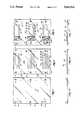
- FIGS. 1-11illustrate the first embodiment of a method according to the present invention.
- FIG. 1is a perspective view illustrating the first step of the first embodiment, and FIGS. 1A, 1B and 1C are transverse sectional views along the plane of line A--A of FIG. 1;
- FIG. 2is a plan view illustrating the product structure after completion of the second step of the method, and FIG. 2A is a transverse sectional view of the product of FIG. 2 along the plane of line A--A;
- FIG. 3is a plan view illustrating the product structure after completion of the third step of the method, and FIG. 3A is a sectional view of the product of FIG. 3 along the plane of line A--A;
- FIG. 4is a plan view illustrating the product structure after completion of the fourth step of the method, and FIG. 4A is a transverse sectional view of the product of FIG. 4 along the line A--A;
- FIG. 5is a plan view illustrating the product structure after completion of the fifth step of the method, and FIG. 5A is a transverse sectional view of the product of FIG. 5 along the plane of line A--A;
- FIG. 6is a plan view, with a portion broken away, illustrating the product structure after completion of the sixth step of the method, and FIG. 6A is a transverse sectional view of the product of FIG. 6 along the plane of line A--A;
- FIG. 7is a plan view illustrating the product structure after completion of the seventh step of the methodand FIG. 7A is a transverse sectional view of the product of FIG. 7 along the plane of line A--A;
- FIG. 8is a plan view illustrating the product structure after completion of the eighth step of the method, and FIG. 8A is a transverse sectional view of the product of FIG. 8 along the plane line A--A;
- FIG. 9is a plan view illustrating the product structure after completion of the ninth step of the method, and FIG. 9A is a transverse sectional view of the product of FIG. 9 along the plane of line A--A;
- FIG. 10is a plan view illustrating the product structure after completion of the tenth step of the method, and FIG. 10A is a transverse sectional view of the product of FIG. 10 along the plane of line A--A; and
- FIG. 11is a perspective view illustrating the last step in the method of the first embodiment.
- FIGS. 12-14illustrate the second embodiment of a method according to the present invention.
- FIG. 12is a plan view illustrating the product structure after completion of the third step of the method of the second embodiment, and FIG. 12A is a transverse sectional view of the product of FIG. 12 along the plane of line A--A;
- FIG. 13is a plan view illustrating the product structure after completion of the fourth step of the method of the second embodiment, and FIG. 13A is a transverse sectional view of the product of FIG. 13 along the plane A--A;
- FIG. 14is a plan view illustrating the product structure after completion of the fifth step of the method of the second embodiment, and FIG. 14A is a transverse sectional view of the product of FIG. 14 along the plane A--A.
- FIG. 15is a sectional view illustrating an alternate arrangement of the second web relative to the substrate web suitable for practice of the invention.
- FIG. 16is a sectional view illustrating an alternate arrangement of the covering layer relative to other webs in the composite structure suitable for the practice of the invention.
- FIG. 17is a plan view illustrating the method of the invention employed to form two columns of electrical membrane panels along a composite web structure.
- FIG. 18is a plan view illustrating the method of the invention employed to form three columns of electrical membrane panels along a composite web structure.
- FIGS. 1-11illustrate the steps involved in a first method of the present invention for the manufacture of a flexible membrane panel including conductive spaced electrical circuits formed on two plastic films.
- the methodincludes performing the various steps in the sequence in which they are described.
- the flexible panel described herein as an example of a type of panel that can be made by the method of this inventionis a touch panel designed to provide an output signal of the X-Y position at which the panel is touched by an operator's finger or a stylus.
- a series of flexible electrical panelsare made on two webs of plastic film laminated together and which remain in web form until the final step of cutting an individual panel from the combined webs.
- the first step of the methodinvolves providing a substrate web 10 of flexible plastic film.
- a plurality of conductive circuitswill be formed on substrate web 10 arranged in one or more longitudinal columns along the web and in transverse rows across the web with there being one or more circuits in each row.
- the webshould be a transparent, or at least translucent, plastic film.
- Any plastic film suitable for membrane switches and touch panelscan be used for substrate web 10, with a polyester film such as Mylar® sold by Dupont being preferred, but other films including nylons, polycarbonates, etc. can be used.
- Web 10can be a thin film, such as on the order of about 2 mils to 10 mils thick; thicker films can be used for the substrate web, but an advantage of the method of the present invention is that it can be employed to form membrane panels on very thin plastic films.
- the web 10can be a single layer of plastic film such as illustrated in the cross-section view of FIG. 1A. Alternate constructions for the web are illustrated in the cross-section views of FIGS. 1B and 1C. As shown in FIG. 1B, the web 10 may include a layer of pressure sensitive adhesive 5 (or other suitable adhesive) coated onto its bottom surface; a release liner 6 is applied over the exposed surface of adhesive 5 so as to protect it during processing and until ready for use. When a panel severed from the web 10 as described later is to be applied to a surface, the liner 6 can be stripped away and the panel adhered to the surface by means of the adhesive layer 5. As shown in FIG.
- a carrier web 7 having a layer of low tack pressure sensitive adhesive 8 along one of its surfacesis joined to the bottom surface of web 10.
- the carriermay be of a material such as paper and will be used to support the web 10 during subsequent processing steps; the carrier (with adhesive 8) is removed after completion of the processing or at the time a panel from the web 10 is to be applied to a surface.
- the web constructions of both FIGS. 1B and 1Cfacilitate the processing of thin films, such as a web 10 of 1 to 3 mils thick in that the liner 6 in the case of FIG. 1B and carrier 7 in the case of FIG. 1C provide physical support for the web 10 during the processing steps.
- Web 10is illustrated in the form of a roll of plastic film in FIG. 1. It should be noted that the web typically will be several hundred feet long to several thousand feet long as a feature of the present invention is to retain substrate web 10 in the form a long web throughout the subsequent process method steps. Thus, web 10 as provided in the initial step of the method should be long enough to accommodate the number of rows of circuits that are to be applied onto the web in subsequent steps and wide enough to cover the number of columns of circuits that are to be formed across the web. Web 10 will be advanced longitudinally for subsequent processing steps as indicated by arrow 9 in FIG. 1.
- the second step of the methodinvolves defining registration means longitudinally along the web 10, with there being one registration means for each row of conductive circuits to be formed on the substrate web.
- the registration means 11 for each rowis illustrated as a rectangular aperture near longitudinal edge 12 of web 10 and a similar longitudinal aperture near longitudinal edge 13 of the web.
- the apertures forming the registration means 11are shown in full line in FIG.2, and three sets thereof are shown in the segment of web 10 in the drawings as there will be three rows of circuits formed on the web as illustrated in the drawings.
- the registration meanscan be in any preselected position relative to each row of circuits to be formed across the substrate web.
- a single rectangular aperture 14can be located along a longitudinal edge of the web for each row of circuits, or a single aperture 15 can be formed along an interior section of the web such as between adjacent rows of circuits.
- the registration meansneed not be apertures formed in the web, but can include printed marks such as the printed cross 16, and there can be one or more such printed registration means located as selected along the substrate web relative to each row of circuits to be formed on the web.
- aperturesWhen apertures are used for the registration means, they can be of any desired configuration instead of the rectangles illustrated in FIG. 1, such as circles, ovals, triangles, etc.
- the registration meansare to be detectable by the equipment used to form conductive circuitry on the substrate, and thus generally should be detectable optically, pneumatically or by other means with various types of printing and/or vacuum deposition equipment.
- the registration meanscan be formed simultaneously with the formation of the conductive first traces described in step (3) which typically would be the case when the registration means are printed marks such as printed cross 13 and the first traces are applied by printing. Also, the registration means can be formed immediately prior to application of the first traces of the web in step (3); thus, for example, apertures 11 can be die cut in the web just prior to the application of the first traces onto the web in step (3).
- the third step of the methodincludes applying the first components of a plurality of conductive first circuits 20 along a surface of substrate web 10.
- the circuits 20are spaced apart from one another, and FIG. 3 shows a single column of circuits 20 along web 10, with one circuit in each row of the column; however, as noted above, there may be two or more columns of circuits applied along the web, and two or more conductive first circuits in each row.
- the components of each circuit 20are applied to the web 20 by aligning with the registration means 11 of the web; thus, as shown in FIG. 3, there is a registration means 11 for each row of first circuits 20 formed on the web.
- Circuits 20can be applied to web 10 by means of vacuum deposition techniques, such as sputtered deposition of metals, metal alloys or conductive compounds, or by printing techniques such as screen printing with conductive inks.
- the first components of each first circuit 20 applied in this step (3)comprises a plurality of evenly spaced conductive first traces 21-27 applied transversely across the web 10 along a selected zone of the web between the registration means 11.
- the sectional view of FIG. 3Aillustrates the manner in which conductive trace 24 has been applied onto surface 10a of the web 10.
- a touch panelwill typically include a large number of traces, but only six traces 21-27 are shown in drawings for clarity of description.
- visual alignment marks 28can be applied onto the web 10 concurrently with application of the first traces on the web and with the same equipment, e.g. screen printer or vacuum deposition equipment, used to apply the traces. Marks 28 can be used to assist the person operating the machinein lining up subsequent passes with the first traces to obtain an initial alignment, bearing in mind, however, that the machine will sense the registration means 11 to accurately align subsequent passes with the first circuits 20.
- Four visual alignment marks 28are depicted in the drawings in association with each first circuit 20, but other configurations, arrangements and number of marks 28 can be used instead of the exemplary disclosure.
- a first dielectric coating 30is applied over selected portions of traces 21-27 of each conductive first circuit 20.
- the first dielectric coating 30is applied as a pattern in the form of a rectangle over end portions of traces 21-27 of each first circuit.
- the coating 30includes an aperture over each trace; thus, coating 30 includes aperture 32 over trace 22, aperture 33 over trace 23, aperture 34 over trace 24, aperture 35 over trace 25, aperture 36 over trace 26, and apertures 31 and 37 over traces 21 and 27 respectively, apertures 31, 37 being arranged in a column.
- any suitable insulating materialcan be used for the dielectric coating 30.
- one or more additional layers of the dielectric coatingcan be applied.
- a first dielectric coating 30is formed in a selected pattern for each first circuit 20 on the substrate web.
- Registration means 11are utilized by the equipment used to form the dielectric coatings to accurately register each coating 30 relative to its respective first circuit 20.
- each first circuit 20comprising a plurality of conductive first leads are formed on the exposed surface 30a of each first dielectric coating 30.
- conductive first leads 41-46are formed, preferably by screen printing of conductive ink, on surface 30a, and there is a lead for each longitudinal column of apertures in the coating 30 applied in step (4).
- Each lead 41-46makes electrical contact through an aperture 31-37 with a respective first trace 21-27 exposed within an aperture.
- lead 41makes electrical contact with first trace 21 within aperture 31 and makes electrical contact with first trace 27 within aperture 37.
- First leads 42-46make similar electrical contact with first traces 22-26, within apertures 32-36, respectively.
- each first lead 41-46has a portion extending onto surface 10a of substrate web 10 on a zone thereof outside the boundary of each first circuit 20.
- each first lead 41-46is L-shaped and includes a longitudinal section A that extends across dielectric coating 30 and across the apertures formed therein, and a transverse section B extending a selected distance along surface 10a of the substrate web and beyond the left boundary of each first circuit 20.
- the first leads 41-36must be accurately positioned with respect to a dielectric coating 30 and the first traces of a first circuit 20 associated therewith.
- the registration means 11are utilized by the equipment used to apply the first leads in order to achieve accurate registration of the first leads relative to the other structure of each first circuit.
- the arrangement of the first traces and first leads of the first circuits 20 described in this first embodiment of the inventionis particularly useful for a membrane panel construction having a large number (e.g. 32 to 100) of first traces and a smaller number (e.g. 16-32) of first leads.
- This type of panel designusually requires that a selected number of first traces, but not all, must be connected to each first lead so as to allow using a 16 or 32 pin connector for connecting external circuitry to the panel.
- the dielectric coating 30is used to prevent shorting between each first lead and the first traces that are not to be connected to it.
- visual longitudinal alignment lines 48 and 49are applied longitudinally on web 10 alongside each first circuit 20, and the lines 48 and 49 are spaced slightly inward of the ends of the transverse sections B of the first leads 41-46; lines 48 and 49 are illustrated in connection with the middle first circuit 20 shown in FIG. 5, but can be applied alongside each row of first circuits.
- Second web 50can be of the same type of plastic film used for substrate web 10, but can be very thin, such as about 1/4 mil to 5 mils thick, preferably about one mil thick when it forms a dielectric layer between circuits of a touch panel.
- Second web 50can include a layer of adhesive, such as pressure sensitive adhesive, thermoplastic adhesive, UV curable adhesive, thermoset adhesive or any other selected adhesive, preferably about 1/4 mil to 5 mils thick, on its surface that is to be joined to the web 10; also, however, suitable adhesive can be first applied to substrate web 10 over a selected zone thereof and second web 50 thereafter joined to the adhesive.
- Second web 50extends longitudinally along substrate web 10, and is shown in this first embodiment as being narrower than the web 10. Second web 50 covers each first circuit 20 formed on web 10, including all or most of the first dielectric coating 30 associated therewith, except for a short connection end portion of the first leads 41-46, indicated as portion B' of first lead41 in FIG. 6, which will be used to connect each first lead to external circuitry as described later.
- Second web 50is joined to web 10 by aligning its edge 51 relative to first leads 41-46.
- the visual alignment lines 48 and 49are employed to assist the person operating the laminating equipment in registering edge 51 of second web 50 in such fashion as to leave connection end portions B' of each first lead exposed.
- the edge 51 of the second webis illustrated as being aligned over outboard line 48.
- the space between lines 48 and 49gives the operator a visual indication of the acceptable tolerance for the edge registration of second web 50. Also, the operator can check the accuracy of the placement of the second web as the laminating equipment is being run by reference to lines 48 and 49.
- the laminating equipmentcan maintain the edge registration, and various other systems can be employed for achieving the appropriate edge registration of web 50 relative to the first leads. Also, it is important that lamination of second web 50 in this step should leave the registrations means 11 exposed or readable by sensing equipment so as to be usable for subsequent steps of the method.
- a plurality of conductive second circuits 60are applied onto the exposed surface 50a of second web 50.
- the application of the first components of second circuitsis illustrated in FIGS. 7 and 7A.
- a conductive second circuit 60is to be applied onto second web 50 over each first circuit 20 formed on the substrate web.
- the first component of each second circuit 60comprises a plurality of evenly spaced conductive second traces that are arranged orthogonal to the first traces of each first circuit 20.
- the second circuitsmay include a large number of second traces, but only five second traces 61-65 are illustrated in the drawings for clarity of description.
- Second circuits 60can be applied to a second web by means of vacuum deposition techniques or by printing techniques such as screen printing; typically, the second circuits will be applied to the web 50 by the same technique employed for formation of first circuits 20 on the substrate web.
- each second trace 61-65has a portion D traversing the first traces 21-27 of circuits 20 and a portion E extending along web 50 beyond the boundary of each first circuit.
- FIGS. 8 and 8Awhich comprises applying a second dielectric coating 70 onto surface 50a of second web 50 that extends over part of end portions E of each second trace 61-65.
- Second dielectric coatingis applied in a pattern to include an aperture over each second trace.
- second dielectric coating 70includes aperture 71 over second trace 61, aperture 72 over trace 62, aperture 73 over trace 63, aperture 74 over trace 64 and aperture 75 over trace 65; the apertures can be arranged with two or more in a column such as illustrated with respect to apertures 72 and 75.
- the second dielectric coatings 70can be of the same composition as first dielectric coatings 30 described above.
- the registration means 11are employed by the equipment used to apply the second dielectric coating to accurately position each second dielectric coating relative to its respective second circuit and the second traces thereof.
- the next step in the process of the inventioncomprises forming the second components of each second circuit comprising a plurality of conductive second leads on each second dielectric coating.
- conductive second leads 81-84are applied over each second dielectric coating 70 to provide a second lead for each transverse row of apertures in a coating 70.
- Each lead 81-84makes electrical contact through an aperture 71-75 with a respective second trace 61-65 within an aperture.
- second lead 81makes electrical contact with second trace 61 within aperture 71.
- second lead 82makes electrical contact with second trace 63 within aperture 73
- second lead 83makes electrical contact with second trace 64 within aperture 74
- second lead 84makes electrical contact with second trace 62 and second trace 65 within apertures 72 and 75, respectively.
- second leads 81-84extend beyond the boundary of a second dielectric coating 70 onto surface 50a of second web 50 to the nearby longitudinal edge 51 of the second web.
- each second lead 81-84has an end portion F on the exposed surface of the second web, as shown by portion F of second lead 81.
- the second leadssuch as leads 81-84, must be accurately registered with respect to the apertures, such as apertures 71-75, in each second dielectric coating 70 and the second traces of each second circuit.
- the registration means 11 defined in the substrate webare employed by the equipment utilized to apply the second traces to achieve accurate positioning thereof in a manner appropriate to the specific equipment used.
- a covering layer 90is applied over the second circuits 60 formed on second web 50.
- Covering layer 90can comprise a web of flexible plastic film laminated over a second web in the manner described previously with respect to lamination of the second web to the substrate web and can be the same type of plastic film material employed for the substrate and second webs although it can be any thin plastic film such as on the order of 1/4 mil to 5 mils thick.
- covering layer 90can be applied in the form of a coating, such as a thermoplastic, thermoset or UV curable coating. Layer 90 should be transparent or translucent when the panels formed by the process are to be transparent.
- Covering layer 90can be used when the membrane panels produced by the method need to be protected against physical damage such as abrasion or an operating environment in which liquids or other foreign matter may be spilled or dropped on the panels. If neither of these conditions is applicable, the covering layer 90 can be omitted.
- Covering layer 90is shown in the first embodiment as being narrower in width than second web 50, particularly along longitudinal edge 51 of the second web. This provides a short connection end portion of each second lead 81-84 on the second web that is exposed between longitudinal edge 91 of covering layer 90 and longitudinal edge 51 of second web 50; the exposed end portions of the second leads are indicated by portion F' of second lead 81. An end portion F' of each second lead will be used for connecting the second leads to external circuitry, as described later.
- Step (10)Upon completion of Step (10), the present method results in a composite web structure comprising second web 50 joined to substrate web 10, with each first circuit on web 10 aligned with a second circuit on web 50 to form a plurality of electronic membrane panels, each including a first circuit and a second circuit and which are arranged in columns and rows along the composite web structure.
- Covering layer 90should be accurately positioned with respect to web 50 and web 10.
- covering layer 90When covering layer 90 is applied as a film laminated to the second web, it can be registered relative to the second web by edge registration in the manner described previously in connection with lamination of second web 50 to substrate web 10. If the covering layer is applied as a coating, the coating is positioned by use of the registration means 11 during application of the covering layer, in whatever manner is appropriate to the specific equipment and type of material used to coat the layer.
- the final step in the method of the inventioninvolves cutting individual touch panels from the composite web structure produced by Steps (1)-(10) of the method as previously described, bearing in mind that the structure obtained upon completion of Step (10) comprises a plurality of touch panels in web form.
- an individual touch panel 100is cut, such as by die cutting, from the composite web structure by cutting transversely across the web structure between each row of first and second circuits, cutting longitudinally through covering layer 90, second web 50 and substrate web 10 along the right edge of each set of first and second circuits, and cutting longitudinally through substrate web 10 along the left edge of each first and second circuit a short distance outboard from the nearby edge 51 of a second web 50.
- the transverse cutscan extend from edge to edge of substrate web 10 to form sheets, and then each sheet can be cut longitudinally to form individual panels.
- An individual panel 100includes a narrow edge portion 101 of the substrate web that is not covered by either the second web or the covering layer and which includes exposed end portions B' of each first lead 42-46. Also, each panel 100 includes a narrow edge portion 102 of second web 50 that is not covered by covering layer 90, and end portions F' of each second lead 81-84 are exposed along edge portion 102 of the second web.
- External drive and sense circuitry to be connected with a touch panel 100are connected to the first circuit 20 of a touch panel along the exposed end portions B' of the first traces thereof, and connected to the second circuit 60 of the panel by connection to the exposed end portions F' of the second traces thereof.
- individual panels 100are accurately cut from the composite web structure by aligning the substrate web with the cutting equipment using the registrations means 11 formed in substrate web 10.
- the method of the invention as described with respect to FIGS. 1-11can be employed to manufacture electrical membrane panels of varying sizes.
- the method of the first embodimentis particularly adapted for the manufacture of large size panels that have a large number of first and second traces and more than one trace is connected to a first or second lead; for example, the method of the first embodiment of the invention was demonstrated during our development work to successfully produce panels approximately 10 inches by 12 inches in size that had 78 first traces, 60 second traces, and 16 each of the first and second leads.
- FIGS. 12-14demonstrates the manner in which the present invention can be used for the manufacture of smaller touch panels, such as those which may have about 16 to 32 first traces and second traces.
- the first step of the second embodiment of the inventionis the same as Step (1) described above with reference to FIG. 1, and the second step of the second embodiment is the same as step (2) described above with respect to FIG. 2 of the first embodiment.
- the third step of the second methodis illustrated in FIG. 12 in plan view and in cross section in FIG. 12A.
- a plurality of first circuits 20are applied onto surface 10a of substrate web 10, each first circuit including a plurality of first traces such as traces 21-26.
- first leads 41-45are formed integral with and at the same time as first traces 21-26, each first trace 41-46 including a longitudinal section A and a transverse section B as illustrated with reference to first lead 46.
- the second embodiment of the inventive methoddoes not employ step (4) of the first embodiment in which a dielectric coating was printed on the substrate web or step (5) of the first embodiment in which first leads were separately applied onto the dielectric coating.
- the fourth step of the second embodimentis that of laminating second web 50 onto substrate web 10 in such fashion as to cover each first circuit 20 formed on the web, including the first leads 41-46 except for the short connection end portion B' of each first lead.
- This step of the second embodimentis carried out in the same manner described above with respect to step (6) of the first embodiment.
- the next step in the method of the second embodiment, as illustrated in FIG. 14,is that of applying a plurality of conductive second circuits 60 on the exposed surface of second web 50.
- Each circuit 60is of the same construction as described previously, and is illustrated as including second traces 61-65 arranged orthogonally to the first traces of the first circuits 20.
- conductive second leads 81-85are formed as elements integral first traces 61-65 and extend transversely across second web 50 to edge 51 of the second web.
- Registration means 11are employed to achieve accurate placement of each second circuit 60 relative to its underlying first circuit 20.
- the second traces and second leadsare formed as integral conductive elements and this embodiment thus eliminates the need to apply a second dielectric coating over the leads and then separately printing second leads on the second dielectric coating as described in steps (8) and (9) of the first method.
- step (10) of the first embodimentwill be the same as step (10) of the first embodiment.
- step (10) of the first embodimentit should again be noted that some uses of the panels to be formed by the method may not require a covering layer.
- step (11) of the first embodimentwherein individual touch panels are cut from the composite web structure resulting from steps (1)-(6).
- This stepcan be carried out in the same manner described previously with respect to the first embodiment.
- the method as set forth in this second embodimentis particularly adapted to the manufacture of panels having a smaller number of first and second traces as compared to the first embodiment in which each trace can be connected to only one lead and the resulting panel will not have an unduly large connection tail or border portion.
- 16 or 32 pin connectorscan be used to connect external sense and drive circuitry to a panel formed by the method of the second embodiment
- the second web 50has been illustrated as being narrower in width than the substrate web 10.
- Thiscan also be accomplished by the composite web structure illustrated in FIG. 15 wherein second web 50 is offset relative to substrate web 10 with its edge 51 arranged relative to connecting end portions B' of the first traces in the manner previously described but with its opposite edge 52 extending beyond the nearby adjacent edge 17 of substrate web 10.
- This featureallows the second web 50 to be of the same width as substrate 10 which will oftentimes facilitate the manufacturing process; also, second web 50 can be wider than web 10.
- a single apertureis used in web 10 as the registration means 11 which is along its edge portion not covered by web 50.
- Covering layer 90has been illustrated and described above as being narrower than second web 50 so as to leave connecting end portions F' of the second leads exposed for connection to external circuitry. This feature also, however, can be provided by employing a covering layer 90 that is wider than second web 50, and this construction is illustrated in FIG. 16. Edge 91 of covering layer 90 is offset from nearby edge 51 of second web 50 so as to expose connecting edge portions F' of the second leads. However, the opposite edge 92 of covering layer 90 can extend beyond the nearby edge 52 of the second web.
- This alternate version of the composite web structurecan be employed when covering layer 90 is a plastic film laminated to the second web. This feature may also facilitate manufacture in that the second web and covering layer films can be of the same width.
- FIGS. 1-14 and described aboveshow a single column of electrical membrane panels formed along the substrate and second webs.
- the method of the inventioncan be employed to form two or more columns of panels along the web composite structure, wherein a row will include more than one panel.
- FIG. 17illustrates a composite web construction which may be employed to form two columns of panels along the web structure.
- FIG. 17illustrates the product formed upon completion of steps (1) through (9) of the first embodiment of the invention previously described, but the structure also can be per steps (1)-(5) of the second embodiment.
- the panels of left column I in FIG. 17will each include a first circuit 20 and second circuit 60 together with connecting leads and dielectric coatings as applicable.
- the panels in the right column II of FIG. 17each include all of the same circuitry except that it will be noted the circuits in this column are oriented at 180° relative to the circuits in column I.
- This arrangementallows a single second web 50 to cover both columns of circuits and still expose the connecting end portions B' of each first lead of the first circuits 20 in column I which extend beyond edge 51 of the second web and also leave exposed the connecting end portions B' of the first leads of the panels of column II which extend beyond the opposite edge 52 of the second web.
- a single covering layer 90(not shown) can be similarly applied so as to expose the connection end portions F' of the leads of the second circuits in columns I and II.
- Individual panelscan be cut from the composite web after completion of the steps subsequent to the product of FIG. 17 by first cutting the composite web into sheets having a row of panels and thereafter cutting individual panels from each sheet.
- FIG. 18illustrates an application of the present method for producing a composite web structure including three columns of electrical membrane panels.
- a third column IIIcan include circuits oriented in the same manner as those of column I as illustrated, or oriented the same as the circuits of column III.
- the circuits of column IIIare spaced from those of columns I and II, and a second web 50' is laminated over the circuits of column III either concurrently with or subsequent to lamination of second web 50 over the circuits of columns I and II.
- the composite web structure of FIG. 18can be cut into sheets in which each sheet includes one row of three panels, and then individual panels are cut from each sheet.
- each panelincludes spaced conductive circuits formed on the surfaces of two separate layers of flexible plastic film wherein the two films remain in elongated web form during the manufacture of the entire membrane panel, following which individual panels are cut from the composite web structure.
- Practice of the new processresults in a web structure that includes a plurality of membrane panels arranged in rows and columns along the composite web structure. For example, during development of the present invention, we have produced panels with the first embodiment of thenew process using elongated substrate and second webs that were 440 feet long on which we applied 350 panels in one column.
- the processprovides an efficient method for manufacturing membrane panels and is especially useful for the production of panels that incorporate at least one very thin film layer, such as a layer as thin as one-quarter mil for the second web, inasmuch as it enables handling very thin plastic films in a manner which will reduce physical damage to the films.
- very thin film layersuch as a layer as thin as one-quarter mil for the second web
- Examples of uses of electronic membrane panels made by the inventive methodinclude transparent touch panels adhered over a display such as a CRT screen, LCD display or plasma display, and digitizer panels which can be opaque or transparent.
- first and second circuits and their associated componentsare arranged at a slight angle in the range of about 5° to 10° to the longitudinal axis of the substrate web when screen printing is employed so as to eliminate squeegee bounce during the printing process due to having a plurality of traces and/or leads oriented perpendicular to the axis of the substrate or second webs.
- any suitable conductive ink typically employed in membrane switch manufacturecan be used, such as conductive ink including silver particles, carbon particles, a blend of silver and carbon particles, etc., of which many suitable types are available commercially.
- a vacuum deposition techniqueis used to apply any of the components of the first or second circuits, indium tin oxide can be applied by vacuum deposition, particularly if a transparent panel is the desired end product, but metals and metal alloys can be applied such as silver, copper, etc.
- the process for producing patterned vacuum deposition coatings as described in commonly-assigned U.S. Pat. Nos. 4,714,631 and 4,895,630is particularly useful when vacuum deposition is used.
Landscapes
- Engineering & Computer Science (AREA)
- Manufacturing & Machinery (AREA)
- Microelectronics & Electronic Packaging (AREA)
- Manufacture Of Switches (AREA)
- Push-Button Switches (AREA)
- Manufacturing Of Electric Cables (AREA)
- Structure Of Printed Boards (AREA)
- Manufacturing Of Printed Wiring (AREA)
Abstract
Description
Claims (8)
Priority Applications (3)
| Application Number | Priority Date | Filing Date | Title |
|---|---|---|---|
| US07/561,027US5062916A (en) | 1990-08-01 | 1990-08-01 | Method for the manufacture of electrical membrane panels having circuits on flexible plastic films |
| EP19910107398EP0471149A3 (en) | 1990-08-01 | 1991-05-07 | Method for the manufacture of electrical membrane panels having circuits on flexible plastic films |
| JP16179791AJP3662261B2 (en) | 1990-08-01 | 1991-07-02 | Method for manufacturing electrical membrane panel |
Applications Claiming Priority (1)
| Application Number | Priority Date | Filing Date | Title |
|---|---|---|---|
| US07/561,027US5062916A (en) | 1990-08-01 | 1990-08-01 | Method for the manufacture of electrical membrane panels having circuits on flexible plastic films |
Publications (1)
| Publication Number | Publication Date |
|---|---|
| US5062916Atrue US5062916A (en) | 1991-11-05 |
Family
ID=24240345
Family Applications (1)
| Application Number | Title | Priority Date | Filing Date |
|---|---|---|---|
| US07/561,027Expired - LifetimeUS5062916A (en) | 1990-08-01 | 1990-08-01 | Method for the manufacture of electrical membrane panels having circuits on flexible plastic films |
Country Status (3)
| Country | Link |
|---|---|
| US (1) | US5062916A (en) |
| EP (1) | EP0471149A3 (en) |
| JP (1) | JP3662261B2 (en) |
Cited By (65)
| Publication number | Priority date | Publication date | Assignee | Title |
|---|---|---|---|---|
| US5234536A (en)* | 1991-04-26 | 1993-08-10 | Olin Corporation | Process for the manufacture of an interconnect circuit |
| US5338392A (en)* | 1992-10-08 | 1994-08-16 | Kabushiki Kaisha Toshiba | Method for manufacturing a laminated plate used in a semiconductor device |
| DE4310809A1 (en)* | 1993-04-02 | 1994-10-06 | Sel Alcatel Ag | Alarm device for a merchandise securing (safeguarding) device |
| US5574430A (en)* | 1994-01-18 | 1996-11-12 | Reinhold Ott | Monitoring sensor |
| US5965848A (en)* | 1997-07-22 | 1999-10-12 | Randice-Lisa Altschul | Disposable portable electronic devices and method of making |
| DE10001942A1 (en)* | 2000-01-18 | 2001-08-09 | Kostal Leopold Gmbh & Co Kg | Multi-layer conductor arrangement e.g. for the manufacture of compact electrical circuits, has at least two electrical conductor layers arranged one above the other on the carrier in different planes |
| US6305073B1 (en)* | 1999-12-29 | 2001-10-23 | Gm Nameplate, Inc. | One-sided electrode arrangement on an intermediate spacer for a touchscreen |
| US6342122B1 (en)* | 2000-08-07 | 2002-01-29 | Ashland Chemical, Inc. | UV post curable pressure sensitive adhesives for membrane switch applications and their Production |
| US20020079134A1 (en)* | 2000-12-21 | 2002-06-27 | Yutaka Kaneda | Processes for manufacturing multilayer flexible wiring boards |
| US6545422B1 (en) | 2000-10-27 | 2003-04-08 | Science Applications International Corporation | Socket for use with a micro-component in a light-emitting panel |
| US6570335B1 (en) | 2000-10-27 | 2003-05-27 | Science Applications International Corporation | Method and system for energizing a micro-component in a light-emitting panel |
| US6612889B1 (en)* | 2000-10-27 | 2003-09-02 | Science Applications International Corporation | Method for making a light-emitting panel |
| US6620012B1 (en) | 2000-10-27 | 2003-09-16 | Science Applications International Corporation | Method for testing a light-emitting panel and the components therein |
| US20030214229A1 (en)* | 2000-11-21 | 2003-11-20 | Holman Andrew W. | Display device and methods of manufacture and control |
| US20030228748A1 (en)* | 2002-05-23 | 2003-12-11 | Nelson Richard A. | Circuit elements having an ink receptive coating and a conductive trace and methods of manufacture |
| US20040004609A1 (en)* | 2000-11-21 | 2004-01-08 | Holman Andrew W. | Display device and methods of manufacture and control |
| US6762124B2 (en) | 2001-02-14 | 2004-07-13 | Avery Dennison Corporation | Method for patterning a multilayered conductor/substrate structure |
| US6762566B1 (en) | 2000-10-27 | 2004-07-13 | Science Applications International Corporation | Micro-component for use in a light-emitting panel |
| US6764367B2 (en) | 2000-10-27 | 2004-07-20 | Science Applications International Corporation | Liquid manufacturing processes for panel layer fabrication |
| US6796867B2 (en) | 2000-10-27 | 2004-09-28 | Science Applications International Corporation | Use of printing and other technology for micro-component placement |
| US6801001B2 (en) | 2000-10-27 | 2004-10-05 | Science Applications International Corporation | Method and apparatus for addressing micro-components in a plasma display panel |
| US6819316B2 (en) | 2001-04-17 | 2004-11-16 | 3M Innovative Properties Company | Flexible capacitive touch sensor |
| US6822626B2 (en) | 2000-10-27 | 2004-11-23 | Science Applications International Corporation | Design, fabrication, testing, and conditioning of micro-components for use in a light-emitting panel |
| US6824857B2 (en) | 2001-04-02 | 2004-11-30 | Nashua Corporation | Circuit elements having an embedded conductive trace and methods of manufacture |
| US6935913B2 (en) | 2000-10-27 | 2005-08-30 | Science Applications International Corporation | Method for on-line testing of a light emitting panel |
| US20050215689A1 (en)* | 2002-06-13 | 2005-09-29 | Arkady Garbar | Nano-powder-based coating and ink compositions |
| US20050214480A1 (en)* | 2002-06-13 | 2005-09-29 | Arkady Garbar | Nano-powder-based coating and ink compositions |
| US20050238804A1 (en)* | 2002-06-13 | 2005-10-27 | Arkady Garbar | Nano-powder-based coating and ink compositions |
| US20060246379A1 (en)* | 2005-05-02 | 2006-11-02 | Jambor George F | Generic patterned conductor for customizable electronic devices |
| US20070013861A1 (en)* | 2005-07-14 | 2007-01-18 | Samsung Electronics Co., Ltd. | Apparatus for and method of manufacturing liquid crystal display |
| US20070113966A1 (en)* | 2004-02-23 | 2007-05-24 | Checkpoint Systems, Inc. | Process for forming at least a portion of a package or an envelope bearing a printed indicia |
| US7288014B1 (en) | 2000-10-27 | 2007-10-30 | Science Applications International Corporation | Design, fabrication, testing, and conditioning of micro-components for use in a light-emitting panel |
| US20080141511A1 (en)* | 2006-12-14 | 2008-06-19 | Ki-Hyun Kim | Methods of forming piezoelectric resonator having resonation structure |
| DE102004038752B4 (en)* | 2004-08-09 | 2009-02-19 | Carl Freudenberg Kg | Touch sensor arrangement and use of a touch sensor arrangement |
| US20090087061A1 (en)* | 2007-09-27 | 2009-04-02 | Siemens Medical Solutions Usa, Inc. | Intrinsic Co-Registration For Modular Multimodality Medical Imaging Systems |
| US20120199464A1 (en)* | 2009-10-15 | 2012-08-09 | Lg Innotek Co., Ltd. | Touch Panel and Manufacturing Method Thereof |
| US20140139763A1 (en)* | 2008-06-06 | 2014-05-22 | Apple Inc. | High resistivity metal fan out |
| EP2772834A3 (en)* | 2011-09-01 | 2014-10-08 | TPK Touch Solutions (Xiamen) Inc. | Touch-on-lens device and method for manufacturing the same |
| US8970537B1 (en) | 2013-09-30 | 2015-03-03 | Synaptics Incorporated | Matrix sensor for image touch sensing |
| US20150059169A1 (en)* | 2013-08-30 | 2015-03-05 | Tianma Micro-Electronics Co., Ltd. | Preparation method of one glass solution touch screen |
| US9081453B2 (en) | 2012-01-12 | 2015-07-14 | Synaptics Incorporated | Single layer capacitive imaging sensors |
| US9081457B2 (en) | 2013-10-30 | 2015-07-14 | Synaptics Incorporated | Single-layer muti-touch capacitive imaging sensor |
| US9274662B2 (en) | 2013-10-18 | 2016-03-01 | Synaptics Incorporated | Sensor matrix pad for performing multiple capacitive sensing techniques |
| US9298325B2 (en) | 2013-09-30 | 2016-03-29 | Synaptics Incorporated | Processing system for a capacitive sensing device |
| US9459367B2 (en) | 2013-10-02 | 2016-10-04 | Synaptics Incorporated | Capacitive sensor driving technique that enables hybrid sensing or equalization |
| US9491852B2 (en) | 2010-10-15 | 2016-11-08 | Apple Inc. | Trace border routing |
| US9542023B2 (en) | 2013-08-07 | 2017-01-10 | Synaptics Incorporated | Capacitive sensing using matrix electrodes driven by routing traces disposed in a source line layer |
| US9690397B2 (en) | 2014-05-20 | 2017-06-27 | Synaptics Incorporated | System and method for detecting an active pen with a matrix sensor |
| US9715304B2 (en) | 2015-06-30 | 2017-07-25 | Synaptics Incorporated | Regular via pattern for sensor-based input device |
| US9720541B2 (en) | 2015-06-30 | 2017-08-01 | Synaptics Incorporated | Arrangement of sensor pads and display driver pads for input device |
| WO2017127346A3 (en)* | 2016-01-21 | 2017-09-08 | 3M Innovative Properties Company | Multi-size touch sensor |
| US9778713B2 (en) | 2015-01-05 | 2017-10-03 | Synaptics Incorporated | Modulating a reference voltage to preform capacitive sensing |
| US9788956B2 (en) | 2009-10-20 | 2017-10-17 | Moximed, Inc. | Extra-articular implantable mechanical energy absorbing assemblies having two deflecting members and methods |
| US9798429B2 (en) | 2014-02-28 | 2017-10-24 | Synaptics Incorporated | Guard electrodes in a sensing stack |
| US9832861B2 (en)* | 2009-10-16 | 2017-11-28 | Lg Innotek Co., Ltd. | Touch panel and manufacturing method thereof |
| US9927832B2 (en) | 2014-04-25 | 2018-03-27 | Synaptics Incorporated | Input device having a reduced border region |
| US9939972B2 (en) | 2015-04-06 | 2018-04-10 | Synaptics Incorporated | Matrix sensor with via routing |
| US10037112B2 (en) | 2015-09-30 | 2018-07-31 | Synaptics Incorporated | Sensing an active device'S transmission using timing interleaved with display updates |
| US10042489B2 (en) | 2013-09-30 | 2018-08-07 | Synaptics Incorporated | Matrix sensor for image touch sensing |
| US10067587B2 (en) | 2015-12-29 | 2018-09-04 | Synaptics Incorporated | Routing conductors in an integrated display device and sensing device |
| US10095948B2 (en) | 2015-06-30 | 2018-10-09 | Synaptics Incorporated | Modulation scheme for fingerprint sensing |
| US10126890B2 (en) | 2015-12-31 | 2018-11-13 | Synaptics Incorporated | Single layer sensor pattern and sensing method |
| US10133421B2 (en) | 2014-04-02 | 2018-11-20 | Synaptics Incorporated | Display stackups for matrix sensor |
| US10175827B2 (en) | 2014-12-23 | 2019-01-08 | Synaptics Incorporated | Detecting an active pen using a capacitive sensing device |
| US10488994B2 (en) | 2015-09-07 | 2019-11-26 | Synaptics Incorporated | Single layer capacitive sensor pattern |
Families Citing this family (2)
| Publication number | Priority date | Publication date | Assignee | Title |
|---|---|---|---|---|
| NL1009976C2 (en)* | 1998-08-31 | 2000-03-02 | Chess Engineering B V | Integrated circuit with electrical contact. |
| GB2541735B (en)* | 2015-08-28 | 2020-05-20 | Novalia Ltd | Fabricating a touch-sensitive input device |
Citations (1)
| Publication number | Priority date | Publication date | Assignee | Title |
|---|---|---|---|---|
| US4935093A (en)* | 1982-06-07 | 1990-06-19 | Max Reeb | Method for the continuous flow make of customized planar electrical circuits |
Family Cites Families (3)
| Publication number | Priority date | Publication date | Assignee | Title |
|---|---|---|---|---|
| IT1182866B (en)* | 1985-09-19 | 1987-10-05 | Istituto Superiore Di Sanita L | APPARATUS FOR THE EVALUATION OF THE TEMPORAL STAGES OF THE TRAVEL OF A DAMAGING SUBJECT AND THE INSTANTANEOUS DISTRIBUTION OF THE BINDING REACTIONS OF THE SOIL |
| DE3814017C1 (en)* | 1988-04-26 | 1989-09-21 | Telenorma Telefonbau Und Normalzeit Gmbh, 6000 Frankfurt, De | Tactile display device for the simultaneous digital transmission of manually generated characters from a transmitter to a receiver |
| US4963702A (en)* | 1989-02-09 | 1990-10-16 | Interlink Electronics, Inc. | Digitizer pad featuring spacial definition of a pressure contact area |
- 1990
- 1990-08-01USUS07/561,027patent/US5062916A/ennot_activeExpired - Lifetime
- 1991
- 1991-05-07EPEP19910107398patent/EP0471149A3/ennot_activeWithdrawn
- 1991-07-02JPJP16179791Apatent/JP3662261B2/ennot_activeExpired - Fee Related
Patent Citations (1)
| Publication number | Priority date | Publication date | Assignee | Title |
|---|---|---|---|---|
| US4935093A (en)* | 1982-06-07 | 1990-06-19 | Max Reeb | Method for the continuous flow make of customized planar electrical circuits |
Cited By (106)
| Publication number | Priority date | Publication date | Assignee | Title |
|---|---|---|---|---|
| US5234536A (en)* | 1991-04-26 | 1993-08-10 | Olin Corporation | Process for the manufacture of an interconnect circuit |
| US5338392A (en)* | 1992-10-08 | 1994-08-16 | Kabushiki Kaisha Toshiba | Method for manufacturing a laminated plate used in a semiconductor device |
| DE4310809A1 (en)* | 1993-04-02 | 1994-10-06 | Sel Alcatel Ag | Alarm device for a merchandise securing (safeguarding) device |
| US5574430A (en)* | 1994-01-18 | 1996-11-12 | Reinhold Ott | Monitoring sensor |
| US5965848A (en)* | 1997-07-22 | 1999-10-12 | Randice-Lisa Altschul | Disposable portable electronic devices and method of making |
| US6305073B1 (en)* | 1999-12-29 | 2001-10-23 | Gm Nameplate, Inc. | One-sided electrode arrangement on an intermediate spacer for a touchscreen |
| DE10001942A1 (en)* | 2000-01-18 | 2001-08-09 | Kostal Leopold Gmbh & Co Kg | Multi-layer conductor arrangement e.g. for the manufacture of compact electrical circuits, has at least two electrical conductor layers arranged one above the other on the carrier in different planes |
| US6342122B1 (en)* | 2000-08-07 | 2002-01-29 | Ashland Chemical, Inc. | UV post curable pressure sensitive adhesives for membrane switch applications and their Production |
| US8043137B2 (en) | 2000-10-27 | 2011-10-25 | Science Applications International Corporation | Light-emitting panel and a method for making |
| US7005793B2 (en) | 2000-10-27 | 2006-02-28 | Science Applications International Corporation | Socket for use with a micro-component in a light-emitting panel |
| US6570335B1 (en) | 2000-10-27 | 2003-05-27 | Science Applications International Corporation | Method and system for energizing a micro-component in a light-emitting panel |
| US6612889B1 (en)* | 2000-10-27 | 2003-09-02 | Science Applications International Corporation | Method for making a light-emitting panel |
| US6620012B1 (en) | 2000-10-27 | 2003-09-16 | Science Applications International Corporation | Method for testing a light-emitting panel and the components therein |
| US6646388B2 (en) | 2000-10-27 | 2003-11-11 | Science Applications International Corporation | Socket for use with a micro-component in a light-emitting panel |
| US7789725B1 (en) | 2000-10-27 | 2010-09-07 | Science Applications International Corporation | Manufacture of light-emitting panels provided with texturized micro-components |
| US6545422B1 (en) | 2000-10-27 | 2003-04-08 | Science Applications International Corporation | Socket for use with a micro-component in a light-emitting panel |
| EP1354332A4 (en)* | 2000-10-27 | 2008-10-29 | Science Applic Int Corp | A light-emitting panel and a method for making |
| US7288014B1 (en) | 2000-10-27 | 2007-10-30 | Science Applications International Corporation | Design, fabrication, testing, and conditioning of micro-components for use in a light-emitting panel |
| US6762566B1 (en) | 2000-10-27 | 2004-07-13 | Science Applications International Corporation | Micro-component for use in a light-emitting panel |
| US6764367B2 (en) | 2000-10-27 | 2004-07-20 | Science Applications International Corporation | Liquid manufacturing processes for panel layer fabrication |
| US6796867B2 (en) | 2000-10-27 | 2004-09-28 | Science Applications International Corporation | Use of printing and other technology for micro-component placement |
| US6801001B2 (en) | 2000-10-27 | 2004-10-05 | Science Applications International Corporation | Method and apparatus for addressing micro-components in a plasma display panel |
| US7140941B2 (en) | 2000-10-27 | 2006-11-28 | Science Applications International Corporation | Liquid manufacturing processes for panel layer fabrication |
| US6822626B2 (en) | 2000-10-27 | 2004-11-23 | Science Applications International Corporation | Design, fabrication, testing, and conditioning of micro-components for use in a light-emitting panel |
| US7137857B2 (en) | 2000-10-27 | 2006-11-21 | Science Applications International Corporation | Method for manufacturing a light-emitting panel |
| US6902456B2 (en) | 2000-10-27 | 2005-06-07 | Science Applications International Corporation | Socket for use with a micro-component in a light-emitting panel |
| US6935913B2 (en) | 2000-10-27 | 2005-08-30 | Science Applications International Corporation | Method for on-line testing of a light emitting panel |
| US7125305B2 (en) | 2000-10-27 | 2006-10-24 | Science Applications International Corporation | Light-emitting panel and a method for making |
| US7025648B2 (en) | 2000-10-27 | 2006-04-11 | Science Applications International Corporation | Liquid manufacturing processes for panel layer fabrication |
| US8246409B2 (en) | 2000-10-27 | 2012-08-21 | Science Applications International Corporation | Light-emitting panel and a method for making |
| US6975068B2 (en) | 2000-10-27 | 2005-12-13 | Science Applications International Corporation | Light-emitting panel and a method for making |
| US20030214229A1 (en)* | 2000-11-21 | 2003-11-20 | Holman Andrew W. | Display device and methods of manufacture and control |
| US20040004609A1 (en)* | 2000-11-21 | 2004-01-08 | Holman Andrew W. | Display device and methods of manufacture and control |
| US7199527B2 (en) | 2000-11-21 | 2007-04-03 | Alien Technology Corporation | Display device and methods of manufacturing and control |
| US7211735B2 (en)* | 2000-12-21 | 2007-05-01 | Sony Corporation | Processes for manufacturing multilayer flexible wiring boards |
| US20020079134A1 (en)* | 2000-12-21 | 2002-06-27 | Yutaka Kaneda | Processes for manufacturing multilayer flexible wiring boards |
| USRE44071E1 (en) | 2001-02-14 | 2013-03-12 | Streaming Sales Llc | Method for patterning a multilayered conductor/substrate structure |
| US6762124B2 (en) | 2001-02-14 | 2004-07-13 | Avery Dennison Corporation | Method for patterning a multilayered conductor/substrate structure |
| US6824857B2 (en) | 2001-04-02 | 2004-11-30 | Nashua Corporation | Circuit elements having an embedded conductive trace and methods of manufacture |
| US6819316B2 (en) | 2001-04-17 | 2004-11-16 | 3M Innovative Properties Company | Flexible capacitive touch sensor |
| US20030228748A1 (en)* | 2002-05-23 | 2003-12-11 | Nelson Richard A. | Circuit elements having an ink receptive coating and a conductive trace and methods of manufacture |
| US7736693B2 (en) | 2002-06-13 | 2010-06-15 | Cima Nanotech Israel Ltd. | Nano-powder-based coating and ink compositions |
| US20050238804A1 (en)* | 2002-06-13 | 2005-10-27 | Arkady Garbar | Nano-powder-based coating and ink compositions |
| US7566360B2 (en)* | 2002-06-13 | 2009-07-28 | Cima Nanotech Israel Ltd. | Nano-powder-based coating and ink compositions |
| US7601406B2 (en)* | 2002-06-13 | 2009-10-13 | Cima Nanotech Israel Ltd. | Nano-powder-based coating and ink compositions |
| US20050215689A1 (en)* | 2002-06-13 | 2005-09-29 | Arkady Garbar | Nano-powder-based coating and ink compositions |
| US20050214480A1 (en)* | 2002-06-13 | 2005-09-29 | Arkady Garbar | Nano-powder-based coating and ink compositions |
| EP1535270A4 (en)* | 2002-08-09 | 2008-09-10 | Science Applic Int Corp | Liquid manufacturing processes for panel layer fabrication |
| US20070113966A1 (en)* | 2004-02-23 | 2007-05-24 | Checkpoint Systems, Inc. | Process for forming at least a portion of a package or an envelope bearing a printed indicia |
| US7856708B2 (en) | 2004-02-23 | 2010-12-28 | Checkpoint Systems, Inc. | Process for forming at least a portion of a package or an envelope bearing a printed indicia |
| DE102004038752B4 (en)* | 2004-08-09 | 2009-02-19 | Carl Freudenberg Kg | Touch sensor arrangement and use of a touch sensor arrangement |
| US20060246379A1 (en)* | 2005-05-02 | 2006-11-02 | Jambor George F | Generic patterned conductor for customizable electronic devices |
| US7745733B2 (en)* | 2005-05-02 | 2010-06-29 | 3M Innovative Properties Company | Generic patterned conductor for customizable electronic devices |
| US20070013861A1 (en)* | 2005-07-14 | 2007-01-18 | Samsung Electronics Co., Ltd. | Apparatus for and method of manufacturing liquid crystal display |
| US20080141511A1 (en)* | 2006-12-14 | 2008-06-19 | Ki-Hyun Kim | Methods of forming piezoelectric resonator having resonation structure |
| US20090087061A1 (en)* | 2007-09-27 | 2009-04-02 | Siemens Medical Solutions Usa, Inc. | Intrinsic Co-Registration For Modular Multimodality Medical Imaging Systems |
| US9069418B2 (en) | 2008-06-06 | 2015-06-30 | Apple Inc. | High resistivity metal fan out |
| US20140139763A1 (en)* | 2008-06-06 | 2014-05-22 | Apple Inc. | High resistivity metal fan out |
| US10048819B2 (en) | 2008-06-06 | 2018-08-14 | Apple Inc. | High resistivity metal fan out |
| US9495048B2 (en)* | 2008-06-06 | 2016-11-15 | Apple Inc. | High resistivity metal fan out |
| US20120199464A1 (en)* | 2009-10-15 | 2012-08-09 | Lg Innotek Co., Ltd. | Touch Panel and Manufacturing Method Thereof |
| US9400577B2 (en)* | 2009-10-15 | 2016-07-26 | Lg Innotek Co., Ltd. | Capactive touch panel |
| US10004138B2 (en) | 2009-10-16 | 2018-06-19 | Lg Innotek Co., Ltd. | Touch panel and manufacturing method thereof |
| US9832861B2 (en)* | 2009-10-16 | 2017-11-28 | Lg Innotek Co., Ltd. | Touch panel and manufacturing method thereof |
| US9788956B2 (en) | 2009-10-20 | 2017-10-17 | Moximed, Inc. | Extra-articular implantable mechanical energy absorbing assemblies having two deflecting members and methods |
| US9491852B2 (en) | 2010-10-15 | 2016-11-08 | Apple Inc. | Trace border routing |
| US9781823B2 (en) | 2010-10-15 | 2017-10-03 | Apple Inc. | Trace border routing |
| EP2772834A3 (en)* | 2011-09-01 | 2014-10-08 | TPK Touch Solutions (Xiamen) Inc. | Touch-on-lens device and method for manufacturing the same |
| TWI456453B (en)* | 2011-09-01 | 2014-10-11 | Tpk Touch Solutions Xiamen Inc | Lens touch device and process method thereof |
| CN102968200B (en)* | 2011-09-01 | 2016-08-03 | 宸美(厦门)光电有限公司 | Eyeglass contactor control device and manufacturing method thereof thereof |
| US9182861B2 (en) | 2012-01-12 | 2015-11-10 | Synaptics Incoporated | Single layer capacitive imaging sensors |
| US9081453B2 (en) | 2012-01-12 | 2015-07-14 | Synaptics Incorporated | Single layer capacitive imaging sensors |
| US9817533B2 (en) | 2012-01-12 | 2017-11-14 | Synaptics Incorporated | Single layer capacitive imaging sensors |
| US9542023B2 (en) | 2013-08-07 | 2017-01-10 | Synaptics Incorporated | Capacitive sensing using matrix electrodes driven by routing traces disposed in a source line layer |
| US9552089B2 (en) | 2013-08-07 | 2017-01-24 | Synaptics Incorporated | Capacitive sensing using a matrix electrode pattern |
| US20150059169A1 (en)* | 2013-08-30 | 2015-03-05 | Tianma Micro-Electronics Co., Ltd. | Preparation method of one glass solution touch screen |
| US9423898B2 (en)* | 2013-08-30 | 2016-08-23 | Shanghai Tianma Micro-electronics Co., Ltd. | Preparation method of one glass solution touch screen |
| US8970537B1 (en) | 2013-09-30 | 2015-03-03 | Synaptics Incorporated | Matrix sensor for image touch sensing |
| US10042489B2 (en) | 2013-09-30 | 2018-08-07 | Synaptics Incorporated | Matrix sensor for image touch sensing |
| US9760212B2 (en) | 2013-09-30 | 2017-09-12 | Synaptics Incorported | Matrix sensor for image touch sensing |
| US9778790B2 (en) | 2013-09-30 | 2017-10-03 | Synaptics Incorporated | Matrix sensor for image touch sensing |
| US10088951B2 (en) | 2013-09-30 | 2018-10-02 | Synaptics Incorporated | Matrix sensor for image touch sensing |
| US9298325B2 (en) | 2013-09-30 | 2016-03-29 | Synaptics Incorporated | Processing system for a capacitive sensing device |
| US9459367B2 (en) | 2013-10-02 | 2016-10-04 | Synaptics Incorporated | Capacitive sensor driving technique that enables hybrid sensing or equalization |
| US9274662B2 (en) | 2013-10-18 | 2016-03-01 | Synaptics Incorporated | Sensor matrix pad for performing multiple capacitive sensing techniques |
| US9081457B2 (en) | 2013-10-30 | 2015-07-14 | Synaptics Incorporated | Single-layer muti-touch capacitive imaging sensor |
| US9483151B2 (en) | 2013-10-30 | 2016-11-01 | Synaptics Incorporated | Single layer multi-touch capacitive imaging sensor |
| US9798429B2 (en) | 2014-02-28 | 2017-10-24 | Synaptics Incorporated | Guard electrodes in a sensing stack |
| US10133421B2 (en) | 2014-04-02 | 2018-11-20 | Synaptics Incorporated | Display stackups for matrix sensor |
| US9927832B2 (en) | 2014-04-25 | 2018-03-27 | Synaptics Incorporated | Input device having a reduced border region |
| US9690397B2 (en) | 2014-05-20 | 2017-06-27 | Synaptics Incorporated | System and method for detecting an active pen with a matrix sensor |
| US10175827B2 (en) | 2014-12-23 | 2019-01-08 | Synaptics Incorporated | Detecting an active pen using a capacitive sensing device |
| US10795471B2 (en) | 2015-01-05 | 2020-10-06 | Synaptics Incorporated | Modulating a reference voltage to perform capacitive sensing |
| US10990148B2 (en) | 2015-01-05 | 2021-04-27 | Synaptics Incorporated | Central receiver for performing capacitive sensing |
| US11693462B2 (en) | 2015-01-05 | 2023-07-04 | Synaptics Incorporated | Central receiver for performing capacitive sensing |
| US9778713B2 (en) | 2015-01-05 | 2017-10-03 | Synaptics Incorporated | Modulating a reference voltage to preform capacitive sensing |
| US9939972B2 (en) | 2015-04-06 | 2018-04-10 | Synaptics Incorporated | Matrix sensor with via routing |
| US10095948B2 (en) | 2015-06-30 | 2018-10-09 | Synaptics Incorporated | Modulation scheme for fingerprint sensing |
| US9720541B2 (en) | 2015-06-30 | 2017-08-01 | Synaptics Incorporated | Arrangement of sensor pads and display driver pads for input device |
| US9715304B2 (en) | 2015-06-30 | 2017-07-25 | Synaptics Incorporated | Regular via pattern for sensor-based input device |
| US10488994B2 (en) | 2015-09-07 | 2019-11-26 | Synaptics Incorporated | Single layer capacitive sensor pattern |
| US10037112B2 (en) | 2015-09-30 | 2018-07-31 | Synaptics Incorporated | Sensing an active device'S transmission using timing interleaved with display updates |
| US10067587B2 (en) | 2015-12-29 | 2018-09-04 | Synaptics Incorporated | Routing conductors in an integrated display device and sensing device |
| US10126890B2 (en) | 2015-12-31 | 2018-11-13 | Synaptics Incorporated | Single layer sensor pattern and sensing method |
| US11093058B2 (en) | 2015-12-31 | 2021-08-17 | Synaptics Incorporated | Single layer sensor pattern and sensing method |
| WO2017127346A3 (en)* | 2016-01-21 | 2017-09-08 | 3M Innovative Properties Company | Multi-size touch sensor |
Also Published As
| Publication number | Publication date |
|---|---|
| JP3662261B2 (en) | 2005-06-22 |
| EP0471149A3 (en) | 1992-03-04 |
| JPH06349372A (en) | 1994-12-22 |
| EP0471149A2 (en) | 1992-02-19 |
Similar Documents
| Publication | Publication Date | Title |
|---|---|---|
| US5062916A (en) | Method for the manufacture of electrical membrane panels having circuits on flexible plastic films | |
| JP7420310B2 (en) | Method for manufacturing conductive film | |
| US20060137813A1 (en) | Registered lamination of webs using laser cutting | |
| US9377918B2 (en) | Method and apparatus for forming patterns in coatings on opposite sides of a transparent substrate | |
| WO2015004970A1 (en) | Touch sensor and method for manufacturing touch sensor | |
| SK279991B6 (en) | Component of printed circuit boards | |
| JP2008140995A (en) | Manufacturing method of multilayer printed wiring board | |
| CN101754575B (en) | Wired circuit board assembly sheet | |
| US6232923B1 (en) | Patch antenna construction | |
| JP2016110179A (en) | Manufacturing method, and quality control method, for touch panels | |
| US5528826A (en) | Method of constructing high yield, fine line, multilayer printed wiring board panel | |
| JP2806721B2 (en) | Liquid crystal display device and manufacturing method thereof | |
| JP3879465B2 (en) | Manufacturing method for inner layer circuit board | |
| JP3740711B2 (en) | Multilayer printed wiring board | |
| JP2586971B2 (en) | Electronic components with flexible substrates | |
| JP3014173B2 (en) | Manufacturing method of flexible printed wiring board | |
| CN119967728A (en) | Design method of inner layer process edge for mixed pressing of different materials | |
| CN207744229U (en) | Bendable circuit base plate | |
| JPH0146887B2 (en) | ||
| JPS61127193A (en) | Printed wiring sheet and making thereof | |
| JPH0384991A (en) | Exposure tool for patterning inner circuit | |
| JPH06283381A (en) | Check mark for detecting layer deviation of layered electronic parts | |
| IES80869B2 (en) | A method for tracking printed circuit boards on multi-board panels through a production process | |
| JPH04120790A (en) | Manufacture of flexible printed circuit board | |
| JPH04144739A (en) | Raw material of laminate and manufacture of laminate |
Legal Events
| Date | Code | Title | Description |
|---|---|---|---|
| AS | Assignment | Owner name:W.H. BRADY CO., A WI CORP., WISCONSIN Free format text:ASSIGNMENT OF ASSIGNORS INTEREST.;ASSIGNORS:AUFDERHEIDE, BRIAN E.;ROBRECHT, MICHAEL J.;KELLEY, WAYNE R.;REEL/FRAME:005406/0570 Effective date:19900727 | |
| STCF | Information on status: patent grant | Free format text:PATENTED CASE | |
| FEPP | Fee payment procedure | Free format text:PAYOR NUMBER ASSIGNED (ORIGINAL EVENT CODE: ASPN); ENTITY STATUS OF PATENT OWNER: LARGE ENTITY | |
| AS | Assignment | Owner name:BRADY USA, INC. A WI CORPORATION Free format text:ASSIGNMENT OF ASSIGNORS INTEREST.;ASSIGNOR:W. H. BRADY CO., A CORPORATION OF WI;REEL/FRAME:005994/0094 Effective date:19920108 Owner name:BRADY USA, INC., WISCONSIN Free format text:ASSIGNMENT OF ASSIGNORS INTEREST;ASSIGNOR:W. H. BRADY CO., A CORPORATION OF WI;REEL/FRAME:005994/0094 Effective date:19920108 | |
| AS | Assignment | Owner name:DYNAPRO THIN FILM PRODUCTS, INC., WISCONSIN Free format text:ASSIGNMENT OF ASSIGNORS INTEREST.;ASSIGNOR:BRADY USA, INC.;REEL/FRAME:006443/0036 Effective date:19930129 | |
| FPAY | Fee payment | Year of fee payment:4 | |
| FPAY | Fee payment | Year of fee payment:8 | |
| FEPP | Fee payment procedure | Free format text:PAYER NUMBER DE-ASSIGNED (ORIGINAL EVENT CODE: RMPN); ENTITY STATUS OF PATENT OWNER: LARGE ENTITY Free format text:PAYOR NUMBER ASSIGNED (ORIGINAL EVENT CODE: ASPN); ENTITY STATUS OF PATENT OWNER: LARGE ENTITY | |
| FPAY | Fee payment | Year of fee payment:12 | |
| AS | Assignment | Owner name:3M DYNAPRO INC., MINNESOTA Free format text:CHANGE OF NAME;ASSIGNOR:DYNAPRO THIN FILMS PRODUCTS INC.;REEL/FRAME:019365/0766 Effective date:20000714 | |
| AS | Assignment | Owner name:3M TOUCH SYSTEMS INC., MASSACHUSETTS Free format text:MERGER;ASSIGNOR:3M DYNAPRO INC.;REEL/FRAME:019382/0564 Effective date:20010630 | |
| AS | Assignment | Owner name:3M INNOVATIVE PROPERTIES COMPANY, MINNESOTA Free format text:ASSIGNMENT OF ASSIGNORS INTEREST;ASSIGNOR:3M TOUCH SYSTEMS INC. A CORPORATION OF THE STATE OF MASSACHUSETTS;REEL/FRAME:019419/0808 Effective date:20070613 |