US5060040A - Photoelectric conversion apparatus - Google Patents
Photoelectric conversion apparatusDownload PDFInfo
- Publication number
- US5060040A US5060040AUS07/269,703US26970388AUS5060040AUS 5060040 AUS5060040 AUS 5060040AUS 26970388 AUS26970388 AUS 26970388AUS 5060040 AUS5060040 AUS 5060040A
- Authority
- US
- United States
- Prior art keywords
- photoelectric conversion
- electrode
- charge storage
- storage section
- layer
- Prior art date
- Legal status (The legal status is an assumption and is not a legal conclusion. Google has not performed a legal analysis and makes no representation as to the accuracy of the status listed.)
- Expired - Lifetime
Links
Images


Classifications
- H—ELECTRICITY
- H10—SEMICONDUCTOR DEVICES; ELECTRIC SOLID-STATE DEVICES NOT OTHERWISE PROVIDED FOR
- H10F—INORGANIC SEMICONDUCTOR DEVICES SENSITIVE TO INFRARED RADIATION, LIGHT, ELECTROMAGNETIC RADIATION OF SHORTER WAVELENGTH OR CORPUSCULAR RADIATION
- H10F39/00—Integrated devices, or assemblies of multiple devices, comprising at least one element covered by group H10F30/00, e.g. radiation detectors comprising photodiode arrays
- H10F39/10—Integrated devices
- H10F39/12—Image sensors
- H10F39/198—Contact-type image sensors [CIS]
- H—ELECTRICITY
- H10—SEMICONDUCTOR DEVICES; ELECTRIC SOLID-STATE DEVICES NOT OTHERWISE PROVIDED FOR
- H10F—INORGANIC SEMICONDUCTOR DEVICES SENSITIVE TO INFRARED RADIATION, LIGHT, ELECTROMAGNETIC RADIATION OF SHORTER WAVELENGTH OR CORPUSCULAR RADIATION
- H10F39/00—Integrated devices, or assemblies of multiple devices, comprising at least one element covered by group H10F30/00, e.g. radiation detectors comprising photodiode arrays
- H10F39/10—Integrated devices
- H10F39/12—Image sensors
- H10F39/18—Complementary metal-oxide-semiconductor [CMOS] image sensors; Photodiode array image sensors
Definitions
- the present inventionrelates to photoelectric conversion apparatus, and more particularly to apparatus suitable for use in a facsimile device, an image reader, a digital copying device or the like which reads image information from an original by moving the document relative to such a device in contact therewith.
- a contact type photoelectric conversion apparatususes an array of rod lenses or focusing fibers to project an image on a document to a photosensor or a group of photosensors including a photoelectric conversion element to thereby read the image.
- photoelectric conversion apparatusFor cost reduction and miniaturization purposes, photoelectric conversion apparatus have recently been developed extensively which include a thin transparent protective layer formed on a photosensor whereby a document is moved in contact with the protective layer to read the document.
- FIG. 1is a schematic of a cross sectional view showing one part of a photoelectric conversion apparatus of this type.
- FIG. 2is an equivalent circuit diagram of one part of the conversion apparatus.
- the light emitted from a light source (not shown) disposed on the back side of a transparent insulating substrate 1is irradiated onto a document 7 through an opening 11 provided on the opposite side of the substrate 1 and the light reflected by the document is now irradiated onto a photoelectric conversion section 12 through a light entrance opening 11.
- the irradiated quantity of light according to the image information of the original 7changes the conductivity of a semiconductor layer correspondingly, the electric charges produced by photoelectric conversion at the photoelectric conversion section 12 (corresponding to Rs in FIG. 2) are stored in an upper layer electrode 6 of an electric charge storage section 13 (corresponding to Cs in FIG. 2).
- the photoelectric conversion section 12 and the electric charge storage section 13include an opaque layer 2 and a lower layer electrode 3, respectively, formed on a common transparent insulating substrate 1.
- the sections 12 and 13further include an insulating layer 4, a semiconductor layer 5 and an upper opaque layer electrode 6 in this order on the layers 2 and 3 with the light entrance opening 11 in the upper layer electrode 6 which constitutes part of the photoelectric conversion section 12.
- the sectionsfurther include in common a plurality of transparent insulating protective layers 301, 302, 303 on the upper layer electrode 6.
- a stray capacitance Cp formed as shown in FIG. 2may cause level shifting of a signal or a malfunction of a signal processor.
- the solution of the above problemsis achieved by a photoelectric conversion apparatus according to the present invention.
- the apparatuscomprises:
- a plurality of photoelectric conversion unitsincluding a semiconductor layer and a pair of first electrodes on an insulating substrate;
- a plurality of electric charge storage sectionswhich include a second electrode, a dielectric layer and a third electrode superposed sequentially on the insulating substrate;
- one of the first electrodes and second electrodesbeing electrically connected and the third electrode being maintained at a constant potential.
- To hold the third electrode at a constant potentialis achieved, for example, by connecting the third electrode to a point of which the potential does not substantially fluctuate, for example, ground.
- the electric charge storage sectionincludes the second electrode, dielectric layer, third electrode, transparent insulating protective layer superposed in this order on the transparent insulating substrate with the first electrode and the second electrode of the photoelectric conversion unit being electrically connected, whereby the electric charges produced by photoelectric conversion at the photoelectric conversion units are stored on the second electrode, and the third electrode is maintained at constant potential.
- the static charges produced on the transparent insulating protective layerare prevented from influencing the second electrode.
- FIG. 1is a schematic cross section view showing an illustrative structure of a conventional image reader.
- FIG. 2is an equivalent circuit diagram of the structure of the conventional image reader.
- FIGS. 3A-3Care schematic illustrations of one embodiment of a photoelectric conversion apparatus according to the present invention.
- FIG. 4is an equivalent circuit diagram of the image reader of the inventive photoelectric conversion apparatus.
- FIGS. 5A to 5Eillustrate the steps of manufacturing the photoelectric conversion apparatus according to the present invention.
- FIG. 6is a schematic of a facsimile device utilizing an embodiment of the photoelectric conversion apparatus according to the present invention.
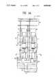
- FIG. 3shows a 2-bit portion of a photoelectric conversion apparatus according to the present invention.
- FIG. 3Ais a plan view of the 2-bit portion
- FIG. 3Bis a cross section view taken along the line B--B' in FIG. 3A
- FIG. 3Cis a cross section view taken along the line C--C' in FIG. 3A.
- FIG. 4is an equivalent circuit diagram of the photoelectric conversion apparatus.
- the photoelectric conversion apparatusincludes a photoelectric conversion unit, an electric charge storage section, a switching thin film transistor section, and a wiring matrix formed integrally on the same substrate. While FIG. 3A shows only the 2-bit structural portion of the apparatus, the actual photoelectric conversion apparatus includes a one-dimensional photoelectric conversion apparatus including a plurality of 1-bit structural portions arranged in a line on the substrate. For example, if the apparatus has to have a resolution of 8 lines/mm through 216 mm corresponding to the width of an A4-size document in the direction transverse to a document P (perpendicular to the direction of movement of the document), it will have 1, 728 photoelectric conversion units arranged.
- the photoelectric conversion units, electric charge storage sections for storing the outputs from the photoelectric conversion units, switching sections for transferring the stored electric charges and processing signals, and required wiring patterns, etc.are formed on the substrate using the same manufacturing steps.
- a matrix wiring section 18Formed on the transparent insulating substrate 1 as shown in FIGS. 3A-C, are a matrix wiring section 18, photoelectric conversion units 12, electric charge storage sections 13, switch sections 20 including a transferring switch 20a and a discharge switch 20b for resetting electric charges in the electric charge storage sections 13, a wiring lead 21 for connecting the signal outputs from the transferring switches 20a to a signal processor to be described later, load capacitors 22 for storing and reading the electric charges transferred by the transferring switches 20a.
- an A-Si: H filmis used as the semiconductor layer 5 which constitutes the photoelectric conversion unit 12, transferring switch 20a and discharge switch 20b.
- a silicon nitride film (SiNH)is formed by glow discharge as the insulating layer 4.
- FIG. 3Aonly electrode wiring in the two upper and lower layers is shown in order to avoid complexity.
- the semiconductor layer 5, insulating layer 4 and transparent insulating layerspassivation layer, adhesion layer, anti-wear layer
- the semiconductor layer 5 and insulating layer 4are formed in the photoelectric conversion units 12, electric charge storage section 13 and switch section 20 as well as between the upper electrodes and the substrate.
- the signal channels output from the respective photoelectric conversion unitsare wired so as not to intersect other wiring leads to thereby prevent crosstalk among signal components and the induction of noise from the gate electrode wiring leads.
- reference numerals 23 and 24each denote the upper electrode and reference numeral 2 the opaque layer.
- the electric charge storage section 13includes lower layer electrode 3, and an insulating layer 4 and semiconductor layer 5 as a dielectric layer formed sequentially in this order on the lower layer electrode 3, and wiring leads continuing to the upper layer electrode 24 of the photoelectric conversion unit 12 and formed on the semiconductor layer 5.
- the electric charge storage section 13has the same structure as a so-called MIS (Metal-Insulator-Semiconductor) capacitor.
- FIG. 3Cshows the switch section 20 of TFT structure including transferring switch 20a and discharge switch 20b.
- the transferring switch 20aincludes lower layer electrode 25 as a gate electrode, insulating layer 4 constituting a gate insulating layer, semiconductor layer 5, upper layer electrode 24 as a source electrode, and upper layer electrode 26 as a drain electrode.
- the gate insulating layer of the discharge switch 20b and the photoconductive semiconductor layerare the same layers as the insulating layer 4 and photoconductive semiconductor layer 5.
- the source electrodeincludes the upper layer electrode 24, the gate electrode includes the lower layer electrode 27, and the drain electrode includes the upper layer electrode 28.
- the lower layer electrode 29is connected to the gate electrode of the transferring switch 20a.
- a transparent insulating layer (passivation A layer) 301which is mainly intended to protect and stabilize the semiconductor layer surface.
- a high-hardness transparent insulating layer 303 called an anti-frictional layeris provided so as to constitute the uppermost layer of the apparatus, which a document directly contacts, in order to protect the entire apparatus from damage caused by the moving document.
- a transparent insulating layer (passivation B layer) 302is formed between the transparent insulating layer 301 and anti-frictional layer in order to improve adhesion and humidity resistance.
- the transparent insulating layer 301is made of a polyimide resin coating
- the transparent insulating layer 302is made of an epoxy resin coating
- the transparent insulating layer 303is made of a microsheet glass of the order of 50 ⁇ m.
- the light emitted by a light source (not shown) disposed on the back side of the transparent insulating substrate 1is irradiated onto a document 7 through the opening 10 provided in the opposite surface of the substrate 1 and reflected by the document 7 so as to be irradiated onto the photoelectric conversion unit 12.
- the light irradiated through the spacing 11 between the upper layer electrodes 23 and 24changes the conductivity of the semiconductor layer 5.
- the electric charges produced by photoelectric conversion at the photoelectric conversion units 12are stored in the electric charge storage section 13 (corresponding Cs in FIG. 4), as in the conventional photoelectric conversion apparatus shown in FIGS. 1 and 2.
- the structure of the present inventionis characterized in that as shown in FIG. 3, the upper layer electrode 6a of the photoelectric conversion unit 12 and the lower electrode 3 of the charge storage section 13 are connected through a throughhole 9, so that the electric charges produced by photoelectric conversion at the photoelectric conversion section 12 are stored in the lower electrode 3 and that the upper layer electrode 6b is connected to a point of which the potential does not substantially fluctuate, for example, to ground GND.
- the transparent insulating protective layer 303 surface which constitutes a static charge generating surface and the lower layer electrode 3 constituting the output of the electric charge storage section 13are connected through capacitors Cpb constituted by the protective layers 301, 302 and 303 and capacitors Cs constituted by the semiconductor layer 5 and insulating layer 4. They, however, are not influenced by possible static charges on the transparent insulating protective layer 303 because the upper layer electrode 6b is connected to GND.
- a stray capacitance Cpa which is formed by the throughhole 9can be reduced to a very small value, so that the protective layer 303 surface and the lower layer electrode 3 are substantially protected from the influence of static electric charges.
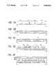
- FIG. 5illustrates the steps of manufacturing the photoelectric conversion apparatus according to the present invention wherein the photoelectric conversion unit 12, the charge storage section 13, a transfer thin film transistor unit 14 which transfers stored charges and a signal line wiring matrix 15 are formed simultaneously.
- the cross section of the photoelectric conversion apparatus in the manufacturing stepsis drawn schematically in FIG. 5 and has no direct corresponding relationship to the apparatus of FIG. 3.
- the apparatus of FIG. 3is manufactured by similar steps.
- a glass baseplatemanufactured by Corning both surfaces of which were polished was cleaned in an ordinary manner using neutral or organic alkali cleaner. Cr (chromium) was then deposited on the baseplate so as to be 0.1 ⁇ m thick by electron beam vapor deposition.
- a desired photoresist patternwas formed of a positive type photoresist (AZ-1370 manufactured by Sipley). Unnecessary Cr portions were then removed by an etching using a mixed aqueous solution of ceric ammonium nitrate and perchloric acid to form the opaque layer 2 of the photoelectric conversion unit, the lower layer electrode 3d of the wiring matrix, the lower layer electrode 3b of the capacitor section and the gate electrode 3c of the thin film transistor section (FIG. 5B).
- the glass baseplate 1was set in a capacitance coupling type glow discharge decomposition device and maintained at 230° C. under an atmosphere of 1 ⁇ 10 -6 Torr. SiH 4 diluted with H 2 to 10% and NH 3 were then fed simultaneously at flow rates of 5 and 20 SCCM, respectively, into the decomposition device. A glow discharge was performed for two hours at 15 W of RF discharge power using a 13.56 MHz high frequency power source to form an insulating layer 4 of silicon nitride having a thickness of 0.3 ⁇ m.
- SiH 4 gaswas then fed at 10 SCCFM, glow discharge was performed for 2.5 hours at a gas pressure of 0.7 Torr and at a discharge power of 8 W to thereby form an amorphous silicon intrinsic layer 5 comprising a semiconductor layer having a thickness of 0.50 ⁇ m.
- a mixed gas of SiH 4 diluted with H 2 to 10% and PH 3 diluted with H 2 to 100 ppm mixed at a ratio of 1:10was used as a source gas to form an n + -layer 17 having a thickness of 0.12 ⁇ which comprises an ohmic contact layer at a discharge power of 30 W (FIG. 5(B)).
- a contact hole patternwas formed of a positive type photoresist (OFPR-1300 manufactured by Tokyo Ooka). Then dry etching was performed using CF 4 gas at a pressure of 0.30 Torr and at an RF discharge power of 100 W by a plasma etching process to eliminate unnecessary portions of the n + -layer and amorphous silicon intrinsic layer and thus to form contact holes 16 (FIG. 5C).
- Aluminumwas deposited so as to be 0.5 ⁇ m thick by an electron beam vapor deposition to form the conductive layer. Subsequently, a desired photoresist pattern was formed and the exposed conductive layer portions were eliminated in a mixed solution of phosphoric acid (aqueous 85% by volume solution), nitride acid (aqueous 60% by volume solution), glacial athetic acid and water mixed at a ratio in volume of 16:1:2:1 to form upper electrodes 6a, 6b, 6c and 6d. Thereafter, dry etching was performed using CF 4 gas by plasma etching process mentioned above to eliminate exposed n + -layer portions to form a desired n + -layer. Then the photoresist was separated (FIG. 5D).
- the transparent insulating protective layer (passivation A layer) 301was formed of polyimide resin on the silicon nitride film. Epoxy resin was coated as the transparent insulating protective layer (passivation B layer) 302, and finally a microglass sheet was adhered to form the transparent insulating protective layer 303 (FIG. 5E).
- FIG. 6is a schematic of a facsimile device using the photoelectric conversion apparatus according to the embodiment as the information processing apparatus.
- a document 205is pressed by a platen roller 203 against a contact type image sensor 201 and moved in the direction of the arrow by the platen roller 203 and a feed roller 204.
- the documentis illuminated by a xenon lamp 202 constituting the light source, the reflected light is incident on the sensor 201 corresponding to the photoelectric conversion apparatus of the particular embodiment of the present invention and converted into an electrical signal corresponding to the image information on the document, and the signal is then transmitted.
- ground lines of the contact type image sensor and the apparatusare electrically connected.
- the upper electrode of the charge storage portionis maintained at a constant voltage.
- a sheet of recording paper 206is carried by a platen roller 207 and an image corresponding to the received signal is reproduced by a thermal head 208 on the sheet of recording paper.
- the entire apparatusis controlled by a controller provided on a system control base base plate 209 and the respective drive systems and circuits are powered by a power source 210.
- the influence on the stored charges of static charges produced on the protective layeris alleviated or suppressed, and level shifting of signals, and the malfunction of signal processors are prevented.
Landscapes
- Solid State Image Pick-Up Elements (AREA)
- Light Receiving Elements (AREA)
Abstract
Description
Claims (12)
Applications Claiming Priority (2)
| Application Number | Priority Date | Filing Date | Title |
|---|---|---|---|
| JP62288199AJP2680002B2 (en) | 1987-11-14 | 1987-11-14 | Photoelectric conversion device |
| JP62-288199 | 1987-11-14 |
Publications (1)
| Publication Number | Publication Date |
|---|---|
| US5060040Atrue US5060040A (en) | 1991-10-22 |
Family
ID=17727095
Family Applications (1)
| Application Number | Title | Priority Date | Filing Date |
|---|---|---|---|
| US07/269,703Expired - LifetimeUS5060040A (en) | 1987-11-14 | 1988-11-10 | Photoelectric conversion apparatus |
Country Status (2)
| Country | Link |
|---|---|
| US (1) | US5060040A (en) |
| JP (1) | JP2680002B2 (en) |
Cited By (22)
| Publication number | Priority date | Publication date | Assignee | Title |
|---|---|---|---|---|
| US5160835A (en)* | 1987-06-12 | 1992-11-03 | Canon Kabushiki Kaisha | Photosensor having conductive shielding layer for electrostatic charge dissipation |
| US5198685A (en)* | 1990-08-01 | 1993-03-30 | Canon Kabushiki Kaisha | Photoelectric conversion apparatus with shock-absorbing layer |
| US5216524A (en)* | 1989-05-18 | 1993-06-01 | Nippon Steel Corporation | Complete-contact type image sensor |
| US5317406A (en)* | 1990-11-07 | 1994-05-31 | Canon Kabushiki Kaisha | Image reading device and image information processing apparatus utilizing the same |
| US5360744A (en)* | 1990-01-11 | 1994-11-01 | Fuji Xerox Co., Ltd. | Method of manufacturing image sensor |
| US5483271A (en)* | 1992-01-08 | 1996-01-09 | Kabushiki Kaisha Toshiba | Electrostatic latent image forming apparatus having a plurality of photoelectric converters |
| US5812109A (en)* | 1994-08-23 | 1998-09-22 | Canon Kabushiki Kaisha | Image input/output apparatus |
| US5841180A (en)* | 1996-03-27 | 1998-11-24 | Canon Kabushiki Kaisha | Photoelectric conversion device, method of driving photoelectric conversion device, and system having the device |
| US5914485A (en)* | 1995-09-05 | 1999-06-22 | Canon Kabushiki Kaisha | Photoelectric converter having respective circuits provided on opposite sides thereof capable of scanning in like directions |
| US6034406A (en)* | 1996-10-24 | 2000-03-07 | Canon Kabushiki Kaisha | Photoelectric conversion apparatus having a shielding member between an arbitrary conversion element and a wavelength converter |
| US6191411B1 (en) | 1997-04-08 | 2001-02-20 | Canon Kabushiki Kaisha | Photoelectric conversion apparatus having drive detection capabilities |
| US6245601B1 (en) | 1997-11-04 | 2001-06-12 | Canon Kabushiki Kaisha | Photoelectric converter, method for driving photoelectric converter and system having photoelectric converter |
| US6295390B1 (en) | 1994-08-23 | 2001-09-25 | Canon Kabushiki Kaisha | Image input/output apparatus with light illumination device for two-dimensional illumination |
| US6384393B2 (en) | 1997-04-10 | 2002-05-07 | Canon Kabushiki Kaisha | Photoelectric conversion device having photoelectric conversion elements |
| US6476867B1 (en) | 1995-09-28 | 2002-11-05 | Canon Kabushiki Kaisha | Photoelectric conversion apparatus, driving method and x-ray image pickup apparatus using the same |
| US6538591B2 (en) | 2000-09-07 | 2003-03-25 | Canon Kabushiki Kaisha | Signal transfer apparatus, and imaging apparatus and radiation image pick-up system using it |
| US20050022856A1 (en)* | 2003-07-08 | 2005-02-03 | Takahiro Komatsu | Organic photoelectric conversion element |
| US6940552B1 (en) | 1999-09-02 | 2005-09-06 | Canon Kabushiki Kaisha | Photoelectric conversion device |
| US7102676B1 (en)* | 1998-10-28 | 2006-09-05 | Canon Kabushiki Kaisha | Image pick-up apparatus and image pick-up system, and method for manufacturing image pick-up apparatus |
| US20080308585A1 (en)* | 2006-09-27 | 2008-12-18 | John Foley | Nozzle |
| US20150179353A1 (en)* | 2013-03-22 | 2015-06-25 | Panasonic Corporation | Photoelectric conversion element |
| US20230157123A1 (en)* | 2020-04-16 | 2023-05-18 | Semiconductor Energy Laboratory Co., Ltd. | Display device, display module, electronic device, and vehicle |
Citations (23)
| Publication number | Priority date | Publication date | Assignee | Title |
|---|---|---|---|---|
| JPS59141264A (en)* | 1983-01-31 | 1984-08-13 | Matsushita Electric Ind Co Ltd | solid-state image sensor |
| US4471371A (en)* | 1981-01-06 | 1984-09-11 | Fuji Xerox Co., Ltd. | Thin film image pickup element |
| JPS60177682A (en)* | 1984-02-23 | 1985-09-11 | Nec Corp | Thin-film-type photoelectric convertion element and production thereof |
| JPS6130069A (en)* | 1984-07-23 | 1986-02-12 | Canon Inc | photo sensor |
| JPS61148870A (en)* | 1984-12-22 | 1986-07-07 | Seiko Epson Corp | solid state imaging device |
| JPS61199660A (en)* | 1985-03-01 | 1986-09-04 | Tokyo Electric Co Ltd | Contact type photoelectric conversion device |
| JPS61289661A (en)* | 1985-06-18 | 1986-12-19 | Mitsubishi Electric Corp | Integrated circuit for driving image sensor |
| US4650984A (en)* | 1984-01-12 | 1987-03-17 | Canon Kabushiki Kaisha | Photosensor array for treating image information |
| US4743955A (en)* | 1985-05-01 | 1988-05-10 | Canon Kabushiki Kaisha | Photoelectric converting device |
| US4746962A (en)* | 1984-08-29 | 1988-05-24 | Semiconductor Energy Laboratory Co., Ltd. | Photoelectric conversion device and method of making the same |
| US4788445A (en)* | 1986-01-24 | 1988-11-29 | Canon Kabushiki Kaisha | Long array photoelectric converting apparatus with insulated matrix wiring |
| US4827146A (en)* | 1986-07-24 | 1989-05-02 | Tokyo Electric Co., Ltd. | Photoelectric conversion element image sensor with combined field effect transistor having compact size |
| US4845355A (en)* | 1985-12-20 | 1989-07-04 | Canon Kabushiki Kaisha | Photoconductive type sensor and its driving method and apparatus |
| US4874957A (en)* | 1987-10-02 | 1989-10-17 | Ricoh Company, Ltd. | Contact type image sensor |
| US4908718A (en)* | 1987-07-09 | 1990-03-13 | Canon Kabushiki Kaisha | Image reading apparatus having a light shielding layer arranged on the sides of the substrate and protective layers of a photo sensor |
| US4910412A (en)* | 1987-04-17 | 1990-03-20 | Stemcor Corporation | Light biased photoresponsive array |
| US4916304A (en)* | 1986-10-07 | 1990-04-10 | Canon Kabushiki Kaisha | Image recording device having a conductive layer formed below a light receiving window |
| US4922117A (en)* | 1987-06-12 | 1990-05-01 | Canon Kabushiki Kaisha | Photoelectric conversion device having a constant potential wiring at the sides of the common wiring |
| US4924282A (en)* | 1986-10-07 | 1990-05-08 | Canon Kabushiki Kaisha | Image reading device with moisture resistant layer |
| US4931661A (en)* | 1986-01-24 | 1990-06-05 | Canon Kabushiki Kaisha | Photoelectric conversion device having a common semiconductor layer for a portion of the photoelectric conversion element and a portion of the transfer transistor section |
| US4937651A (en)* | 1985-08-24 | 1990-06-26 | Semiconductor Energy Laboratory Co., Ltd. | Semiconductor device free from the current leakage through a semiconductor layer and method for manufacturing same |
| US4953000A (en)* | 1987-11-14 | 1990-08-28 | Canon Kabushiki Kaisha | Semiconductor device |
| US4982079A (en)* | 1987-06-12 | 1991-01-01 | Canon Kabushiki Kaisha | Photo-sensor having plural transparent layers and a conductive layer to reduce electrostaslic charges |
Family Cites Families (3)
| Publication number | Priority date | Publication date | Assignee | Title |
|---|---|---|---|---|
| JPS61218167A (en)* | 1985-03-25 | 1986-09-27 | Canon Inc | line sensor |
| JPS61263157A (en)* | 1985-05-16 | 1986-11-21 | Fuji Electric Co Ltd | image sensor |
| JPS6182570A (en)* | 1985-05-31 | 1986-04-26 | Kyocera Corp | reader |
- 1987
- 1987-11-14JPJP62288199Apatent/JP2680002B2/ennot_activeExpired - Fee Related
- 1988
- 1988-11-10USUS07/269,703patent/US5060040A/ennot_activeExpired - Lifetime
Patent Citations (24)
| Publication number | Priority date | Publication date | Assignee | Title |
|---|---|---|---|---|
| US4471371A (en)* | 1981-01-06 | 1984-09-11 | Fuji Xerox Co., Ltd. | Thin film image pickup element |
| JPS59141264A (en)* | 1983-01-31 | 1984-08-13 | Matsushita Electric Ind Co Ltd | solid-state image sensor |
| US4650984A (en)* | 1984-01-12 | 1987-03-17 | Canon Kabushiki Kaisha | Photosensor array for treating image information |
| JPS60177682A (en)* | 1984-02-23 | 1985-09-11 | Nec Corp | Thin-film-type photoelectric convertion element and production thereof |
| JPS6130069A (en)* | 1984-07-23 | 1986-02-12 | Canon Inc | photo sensor |
| US4746962A (en)* | 1984-08-29 | 1988-05-24 | Semiconductor Energy Laboratory Co., Ltd. | Photoelectric conversion device and method of making the same |
| JPS61148870A (en)* | 1984-12-22 | 1986-07-07 | Seiko Epson Corp | solid state imaging device |
| JPS61199660A (en)* | 1985-03-01 | 1986-09-04 | Tokyo Electric Co Ltd | Contact type photoelectric conversion device |
| US4743955A (en)* | 1985-05-01 | 1988-05-10 | Canon Kabushiki Kaisha | Photoelectric converting device |
| JPS61289661A (en)* | 1985-06-18 | 1986-12-19 | Mitsubishi Electric Corp | Integrated circuit for driving image sensor |
| US4937651A (en)* | 1985-08-24 | 1990-06-26 | Semiconductor Energy Laboratory Co., Ltd. | Semiconductor device free from the current leakage through a semiconductor layer and method for manufacturing same |
| US4845355A (en)* | 1985-12-20 | 1989-07-04 | Canon Kabushiki Kaisha | Photoconductive type sensor and its driving method and apparatus |
| US4931661A (en)* | 1986-01-24 | 1990-06-05 | Canon Kabushiki Kaisha | Photoelectric conversion device having a common semiconductor layer for a portion of the photoelectric conversion element and a portion of the transfer transistor section |
| US4788445A (en)* | 1986-01-24 | 1988-11-29 | Canon Kabushiki Kaisha | Long array photoelectric converting apparatus with insulated matrix wiring |
| US4827146A (en)* | 1986-07-24 | 1989-05-02 | Tokyo Electric Co., Ltd. | Photoelectric conversion element image sensor with combined field effect transistor having compact size |
| US4916304A (en)* | 1986-10-07 | 1990-04-10 | Canon Kabushiki Kaisha | Image recording device having a conductive layer formed below a light receiving window |
| US4924282A (en)* | 1986-10-07 | 1990-05-08 | Canon Kabushiki Kaisha | Image reading device with moisture resistant layer |
| US4910412A (en)* | 1987-04-17 | 1990-03-20 | Stemcor Corporation | Light biased photoresponsive array |
| US4922117A (en)* | 1987-06-12 | 1990-05-01 | Canon Kabushiki Kaisha | Photoelectric conversion device having a constant potential wiring at the sides of the common wiring |
| US4939592A (en)* | 1987-06-12 | 1990-07-03 | Canon Kabushiki Kaisha | Contact photoelectric conversion device |
| US4982079A (en)* | 1987-06-12 | 1991-01-01 | Canon Kabushiki Kaisha | Photo-sensor having plural transparent layers and a conductive layer to reduce electrostaslic charges |
| US4908718A (en)* | 1987-07-09 | 1990-03-13 | Canon Kabushiki Kaisha | Image reading apparatus having a light shielding layer arranged on the sides of the substrate and protective layers of a photo sensor |
| US4874957A (en)* | 1987-10-02 | 1989-10-17 | Ricoh Company, Ltd. | Contact type image sensor |
| US4953000A (en)* | 1987-11-14 | 1990-08-28 | Canon Kabushiki Kaisha | Semiconductor device |
Cited By (48)
| Publication number | Priority date | Publication date | Assignee | Title |
|---|---|---|---|---|
| US5160835A (en)* | 1987-06-12 | 1992-11-03 | Canon Kabushiki Kaisha | Photosensor having conductive shielding layer for electrostatic charge dissipation |
| US5216524A (en)* | 1989-05-18 | 1993-06-01 | Nippon Steel Corporation | Complete-contact type image sensor |
| US5360744A (en)* | 1990-01-11 | 1994-11-01 | Fuji Xerox Co., Ltd. | Method of manufacturing image sensor |
| US5198685A (en)* | 1990-08-01 | 1993-03-30 | Canon Kabushiki Kaisha | Photoelectric conversion apparatus with shock-absorbing layer |
| US5317406A (en)* | 1990-11-07 | 1994-05-31 | Canon Kabushiki Kaisha | Image reading device and image information processing apparatus utilizing the same |
| US5483271A (en)* | 1992-01-08 | 1996-01-09 | Kabushiki Kaisha Toshiba | Electrostatic latent image forming apparatus having a plurality of photoelectric converters |
| US6295390B1 (en) | 1994-08-23 | 2001-09-25 | Canon Kabushiki Kaisha | Image input/output apparatus with light illumination device for two-dimensional illumination |
| US5812109A (en)* | 1994-08-23 | 1998-09-22 | Canon Kabushiki Kaisha | Image input/output apparatus |
| US20080224058A1 (en)* | 1995-09-05 | 2008-09-18 | Canon Kabushiki Kaisha | Photoelectric converter and x-ray image pick-up device |
| US7635835B2 (en) | 1995-09-05 | 2009-12-22 | Canon Kabushiki Kaisha | Photoelectric converter and x-ray image pick-up device |
| US8274033B2 (en) | 1995-09-05 | 2012-09-25 | Canon Kabushiki Kaisha | Photoelectric converter |
| US20110147598A1 (en)* | 1995-09-05 | 2011-06-23 | Canon Kabushiki Kaisha | Photoelectric converter |
| US5914485A (en)* | 1995-09-05 | 1999-06-22 | Canon Kabushiki Kaisha | Photoelectric converter having respective circuits provided on opposite sides thereof capable of scanning in like directions |
| US6297493B1 (en) | 1995-09-05 | 2001-10-02 | Canon Kabushiki Kaisha | Photoelectric converter with a plurality of photoelectric conversion layers deposited in a predetermined orientation relative to one another |
| US7915573B2 (en) | 1995-09-05 | 2011-03-29 | Canon Kabushiki Kaisha | Photoelectric converter and X-ray image pick-up device |
| US7170042B2 (en) | 1995-09-05 | 2007-01-30 | Canon Kabushiki Kaisha | Photoelectric converter and X-ray image pick-up device |
| US20070114363A1 (en)* | 1995-09-05 | 2007-05-24 | Canon Kabushiki Kaisha | Photoelectric converter and x-ray image pick-up device |
| US7381938B2 (en) | 1995-09-05 | 2008-06-03 | Canon Kabushiki Kaisha | Photoelectric converter and x-ray image pick-up device |
| US6664527B2 (en) | 1995-09-05 | 2003-12-16 | Canon Kabushiki Kaisha | Photoelectric converter and X-ray image pick-up device |
| US20040108463A1 (en)* | 1995-09-05 | 2004-06-10 | Canon Kabushiki Kaisha | Photoelectric converter and X-ray image pick-up device |
| US20080001091A1 (en)* | 1995-09-05 | 2008-01-03 | Canon Kabushiki Kaisha | Photoelectric converter and x-ray image pick-up device |
| US7285765B2 (en) | 1995-09-05 | 2007-10-23 | Canon Kabushiki Kaisha | Photoelectric converter and X-ray image pick-up device |
| US6476867B1 (en) | 1995-09-28 | 2002-11-05 | Canon Kabushiki Kaisha | Photoelectric conversion apparatus, driving method and x-ray image pickup apparatus using the same |
| US5841180A (en)* | 1996-03-27 | 1998-11-24 | Canon Kabushiki Kaisha | Photoelectric conversion device, method of driving photoelectric conversion device, and system having the device |
| US6034406A (en)* | 1996-10-24 | 2000-03-07 | Canon Kabushiki Kaisha | Photoelectric conversion apparatus having a shielding member between an arbitrary conversion element and a wavelength converter |
| US6191411B1 (en) | 1997-04-08 | 2001-02-20 | Canon Kabushiki Kaisha | Photoelectric conversion apparatus having drive detection capabilities |
| US6384393B2 (en) | 1997-04-10 | 2002-05-07 | Canon Kabushiki Kaisha | Photoelectric conversion device having photoelectric conversion elements |
| US20020070344A1 (en)* | 1997-04-10 | 2002-06-13 | Eiichi Takami | Photoelectric conversion device |
| US20070108372A1 (en)* | 1997-04-10 | 2007-05-17 | Canon Kabushiki Kaisha | Photoelectric conversion device for reducing radiation noise on large screen sensors |
| US7164112B2 (en) | 1997-04-10 | 2007-01-16 | Canon Kabushiki Kaisha | Photoelectric conversion device for reducing radiation noise on large screen sensors |
| US7663082B2 (en) | 1997-04-10 | 2010-02-16 | Canon Kabushiki Kaisha | Photoelectric conversion device for reducing radiation noise on large screen sensors |
| US7009164B2 (en) | 1997-11-04 | 2006-03-07 | Canon Kabushiki Kaisha | Photoelectric converter method for driving photoelectric converter and system having photoelectric converter for image formation converted from radiation |
| US6245601B1 (en) | 1997-11-04 | 2001-06-12 | Canon Kabushiki Kaisha | Photoelectric converter, method for driving photoelectric converter and system having photoelectric converter |
| US20050156115A1 (en)* | 1997-11-04 | 2005-07-21 | Canon Kabushiki Kaisha | Photoelectric converter, method for driving photoelectric converter and system having photoelectric converter |
| US6867469B2 (en) | 1997-11-04 | 2005-03-15 | Canon Kabushiki Kaisha | Photoelectric converter, method for driving photoelectric converter and system having photoelectric converter |
| US20070075247A1 (en)* | 1998-10-28 | 2007-04-05 | Canon Kabushiki Kaisha | Image pick-up apparatus and image pick-up system, and method for manufacturing image pick-up apparatus |
| US7102676B1 (en)* | 1998-10-28 | 2006-09-05 | Canon Kabushiki Kaisha | Image pick-up apparatus and image pick-up system, and method for manufacturing image pick-up apparatus |
| US7852392B2 (en) | 1998-10-28 | 2010-12-14 | Canon Kabushiki Kaisha | Image pick-up apparatus and image pick-up system, and method for manufacturing image pick-up apparatus |
| US20050194624A1 (en)* | 1999-09-02 | 2005-09-08 | Canon Kabushiki Kaisha | Photoelectric conversion device and method of driving the same |
| US7616244B2 (en) | 1999-09-02 | 2009-11-10 | Canon Kabushiki Kaisha | Photoelectric conversion device and method of driving the same |
| US6940552B1 (en) | 1999-09-02 | 2005-09-06 | Canon Kabushiki Kaisha | Photoelectric conversion device |
| US6538591B2 (en) | 2000-09-07 | 2003-03-25 | Canon Kabushiki Kaisha | Signal transfer apparatus, and imaging apparatus and radiation image pick-up system using it |
| US20050022856A1 (en)* | 2003-07-08 | 2005-02-03 | Takahiro Komatsu | Organic photoelectric conversion element |
| US7180110B2 (en)* | 2003-07-08 | 2007-02-20 | Matsushita Electric Industrial Co., Ltd. | Organic photoelectric conversion element |
| US20080308585A1 (en)* | 2006-09-27 | 2008-12-18 | John Foley | Nozzle |
| US20150179353A1 (en)* | 2013-03-22 | 2015-06-25 | Panasonic Corporation | Photoelectric conversion element |
| US9159500B2 (en)* | 2013-03-22 | 2015-10-13 | Panasonic Corporation | Photoelectric conversion element |
| US20230157123A1 (en)* | 2020-04-16 | 2023-05-18 | Semiconductor Energy Laboratory Co., Ltd. | Display device, display module, electronic device, and vehicle |
Also Published As
| Publication number | Publication date |
|---|---|
| JPH01129472A (en) | 1989-05-22 |
| JP2680002B2 (en) | 1997-11-19 |
Similar Documents
| Publication | Publication Date | Title |
|---|---|---|
| US5060040A (en) | Photoelectric conversion apparatus | |
| JP2702131B2 (en) | Image reading apparatus and image information reading apparatus having the same | |
| US6570197B2 (en) | Optical device having sensing TGTs and switching TFTs with different active layer thickness | |
| US5338690A (en) | Photoelectronic conversion device | |
| US4931661A (en) | Photoelectric conversion device having a common semiconductor layer for a portion of the photoelectric conversion element and a portion of the transfer transistor section | |
| US4288702A (en) | Image pickup device having electrode matrix coupling | |
| US5202575A (en) | TFT-driven image sensor including a reduced-size capacitor structure | |
| US4924282A (en) | Image reading device with moisture resistant layer | |
| US4650984A (en) | Photosensor array for treating image information | |
| US4874957A (en) | Contact type image sensor | |
| US4857751A (en) | Photoelectric conversion apparatus with separating electrodes | |
| US5061979A (en) | Semiconductor photoelectric device having a matrix wiring section | |
| EP0297413B1 (en) | Photoelectric conversion device | |
| US5128532A (en) | Image reading device having a conductive layer formed below a light receiving window | |
| US4541015A (en) | Two-dimensional image readout device | |
| US5366921A (en) | Process for fabricating an electronic circuit apparatus | |
| US4567374A (en) | Photoelectric converting device with a plurality of divided electrodes | |
| US4953000A (en) | Semiconductor device | |
| JPH07107931B2 (en) | Photoelectric conversion device manufacturing method | |
| JP2959854B2 (en) | Image reading device | |
| JP2815134B2 (en) | Image reading apparatus and image information reading apparatus having the same | |
| JPH0732245B2 (en) | Photosensor manufacturing method | |
| JPH04367271A (en) | Manufacturing method of photoelectric conversion device | |
| JP2907238B2 (en) | Image reading device | |
| JP2625540B2 (en) | Semiconductor device, photoelectric conversion device, and manufacturing method thereof |
Legal Events
| Date | Code | Title | Description |
|---|---|---|---|
| AS | Assignment | Owner name:CANON KABUSHIKI KAISHA, 30-2, 3-CHOME, SHIMOMARUKO Free format text:ASSIGNMENT OF ASSIGNORS INTEREST.;ASSIGNORS:SAIKA, TOSHIHIRO;KAIFU, NORIYUKI;REEL/FRAME:004973/0451 Effective date:19881102 Owner name:CANON KABUSHIKI KAISHA, A CORP. OF JAPAN, JAPAN Free format text:ASSIGNMENT OF ASSIGNORS INTEREST;ASSIGNORS:SAIKA, TOSHIHIRO;KAIFU, NORIYUKI;REEL/FRAME:004973/0451 Effective date:19881102 | |
| STCF | Information on status: patent grant | Free format text:PATENTED CASE | |
| CC | Certificate of correction | ||
| FEPP | Fee payment procedure | Free format text:PAYOR NUMBER ASSIGNED (ORIGINAL EVENT CODE: ASPN); ENTITY STATUS OF PATENT OWNER: LARGE ENTITY | |
| FPAY | Fee payment | Year of fee payment:4 | |
| FEPP | Fee payment procedure | Free format text:PAYOR NUMBER ASSIGNED (ORIGINAL EVENT CODE: ASPN); ENTITY STATUS OF PATENT OWNER: LARGE ENTITY Free format text:PAYER NUMBER DE-ASSIGNED (ORIGINAL EVENT CODE: RMPN); ENTITY STATUS OF PATENT OWNER: LARGE ENTITY | |
| FPAY | Fee payment | Year of fee payment:8 | |
| FPAY | Fee payment | Year of fee payment:12 |