US5058995A - Pixel electrode structure for liquid crystal display devices - Google Patents
Pixel electrode structure for liquid crystal display devicesDownload PDFInfo
- Publication number
- US5058995A US5058995AUS07/493,604US49360490AUS5058995AUS 5058995 AUS5058995 AUS 5058995AUS 49360490 AUS49360490 AUS 49360490AUS 5058995 AUS5058995 AUS 5058995A
- Authority
- US
- United States
- Prior art keywords
- pixel electrode
- solid state
- state material
- electrode structure
- drain
- Prior art date
- Legal status (The legal status is an assumption and is not a legal conclusion. Google has not performed a legal analysis and makes no representation as to the accuracy of the status listed.)
- Expired - Lifetime
Links
- 239000004973liquid crystal related substanceSubstances0.000titleclaimsabstractdescription23
- 239000000463materialSubstances0.000claimsabstractdescription39
- 239000007787solidSubstances0.000claimsabstractdescription32
- 239000010409thin filmSubstances0.000claimsabstractdescription6
- 229910021417amorphous siliconInorganic materials0.000claimsdescription11
- 229910021420polycrystalline siliconInorganic materials0.000claimsdescription11
- 229920005591polysiliconPolymers0.000claimsdescription11
- 239000000758substrateSubstances0.000claimsdescription11
- 239000011248coating agentSubstances0.000claims4
- 238000000576coating methodMethods0.000claims4
- 210000002858crystal cellAnatomy0.000description3
- 238000004519manufacturing processMethods0.000description3
- ZOKXTWBITQBERF-UHFFFAOYSA-NMolybdenumChemical compound[Mo]ZOKXTWBITQBERF-UHFFFAOYSA-N0.000description2
- 239000003086colorantSubstances0.000description2
- 230000007423decreaseEffects0.000description2
- 239000011159matrix materialSubstances0.000description2
- 229910052750molybdenumInorganic materials0.000description2
- 239000011733molybdenumSubstances0.000description2
- RTAQQCXQSZGOHL-UHFFFAOYSA-NTitaniumChemical compound[Ti]RTAQQCXQSZGOHL-UHFFFAOYSA-N0.000description1
- 230000005540biological transmissionEffects0.000description1
- 210000004027cellAnatomy0.000description1
- 230000003247decreasing effectEffects0.000description1
- 230000008030eliminationEffects0.000description1
- 238000003379elimination reactionMethods0.000description1
- 239000012212insulatorSubstances0.000description1
- 238000002955isolationMethods0.000description1
- XOLBLPGZBRYERU-UHFFFAOYSA-Ntin dioxideChemical compoundO=[Sn]=OXOLBLPGZBRYERU-UHFFFAOYSA-N0.000description1
- 229910001887tin oxideInorganic materials0.000description1
- 229910052719titaniumInorganic materials0.000description1
- 239000010936titaniumSubstances0.000description1
- 230000000007visual effectEffects0.000description1
Images


Classifications
- G—PHYSICS
- G02—OPTICS
- G02F—OPTICAL DEVICES OR ARRANGEMENTS FOR THE CONTROL OF LIGHT BY MODIFICATION OF THE OPTICAL PROPERTIES OF THE MEDIA OF THE ELEMENTS INVOLVED THEREIN; NON-LINEAR OPTICS; FREQUENCY-CHANGING OF LIGHT; OPTICAL LOGIC ELEMENTS; OPTICAL ANALOGUE/DIGITAL CONVERTERS
- G02F1/00—Devices or arrangements for the control of the intensity, colour, phase, polarisation or direction of light arriving from an independent light source, e.g. switching, gating or modulating; Non-linear optics
- G02F1/01—Devices or arrangements for the control of the intensity, colour, phase, polarisation or direction of light arriving from an independent light source, e.g. switching, gating or modulating; Non-linear optics for the control of the intensity, phase, polarisation or colour
- G02F1/13—Devices or arrangements for the control of the intensity, colour, phase, polarisation or direction of light arriving from an independent light source, e.g. switching, gating or modulating; Non-linear optics for the control of the intensity, phase, polarisation or colour based on liquid crystals, e.g. single liquid crystal display cells
- G02F1/133—Constructional arrangements; Operation of liquid crystal cells; Circuit arrangements
- G02F1/136—Liquid crystal cells structurally associated with a semi-conducting layer or substrate, e.g. cells forming part of an integrated circuit
- G02F1/1362—Active matrix addressed cells
- G02F1/1368—Active matrix addressed cells in which the switching element is a three-electrode device
Definitions
- This inventionrelates generally to liquid crystal display devices and particularly to a pixel electrode structure for such devices.
- Liquid crystal display devicesare composed of a matrix of pixels arranged horizontally in rows and vertically in columns.
- the individual liquid crystalsare defined by transparent electrodes which determine the configuration of the liquid crystal cell.
- each liquid crystal cellis associated with a thin film transistor (TFT), or other solid state switching device, which serves as a switch to selectively turn the liquid crystals on and off.
- Select linesrun horizontally between the rows of pixel electrodes and the gates of the TFTs are coupled to the select lines. Accordingly, a complete horizontal row of pixel electrodes is simultaneously "turned on” upon the selection of a particular select line.
- Data linesrun vertically between the columns of pixel electrodes and are used to apply the display producing data signals to the pixel electrodes of a particular column. However only the pixels which are associated with energized TFTs receive the data signals. The display is therefore produced one line at a time.
- the source of the TFTis electrically coupled to the drive line and the drain of the TFT is coupled to the pixel electrode.
- space for the TFTsis provided by removing a corner of the pixel electrodes and fabricating the TFTs in the vacated areas.
- Thisis disadvantageous because the pixel electrodes are transparent to light while the TFTs are not. Accordingly, the corner of the pixel electrode which is removed to provide space for the TFTs is no longer transparent to light and the amount of light passing through the electrode is decreased by the same percentage as the percentage of decrease in the area of the electrode.
- a liquid crystal pixel electrode structureincludes a select line supported on a substrate and coated with an insulative material.
- a region of undoped solid state materialoverlays a length of the select line.
- a source area of doped solid state materialoverlays a first portion of the region and extends beyond the select line.
- a drain area of doped solid state materialoverlays a second portion of the region and is spaced from the source area to form a channel between the source and drain areas.
- a data lineis in electrical contact with the source area and extends substantially perpendicular to the select line.
- a pixel electrode having a first continuous uninterrupted sideis in electrical contact with the drain area and also has a second continuous, uninterrupted side spaced from the data line.
- a notchpasses through the undoped solid state material and is positioned between the data line and the drain area to prevent leakage between the source area/data line and the drain area.
- FIG. 1shows a prior art pixel electrode and thin film transistor structure.
- FIG. 1ais an equivalent circuit of the structure of FIG. 1.
- FIG. 2is a preferred embodiment of the present invention.
- FIG. 2ais an equivalent circuit of the preferred embodiment of FIG. 2.
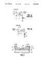
- FIG. 3is a cross section taken on line 3--3 of FIG. 2.
- FIG. 1is a prior art arrangement of a thin film transistor (TFT) for connecting the pixel electrode of a liquid crystal device to the select line and data lines of the device.
- a pixel electrode 11has a corner 12 removed to provide space for a thin film transistor (TFT) 13 which couples the pixel electrode 11 to a data line 14 and a select line 15.
- the TFT 13includes a drain 16 which is in electrical contact with the pixel electrode 11.
- the TFTalso includes a source 17 which is in electrical contact with the drive line 14.
- the gate 18 of the TFT 13is an electrical contact with the select line 15. Additional TFTs 13 are shown for adjacent pixel electrodes, only portions of which are shown.
- the select line 15is voltage biased to apply a voltage to the gates 18 of the TFTs 13 thereby turning on all of the TFTs which are electrically connected to the biased select line.
- the video signals which are to be imposed upon the pixel electrodes 11are applied by the various data lines 14 to charge the liquid crystal devices to the voltages needed to produce the desired display.
- the voltageis applied to the pixel electrodes 11 the liquid crystal material molecules realign and the liquid crystal material becomes light transparent. Accordingly, light from a backlighting system (not shown) passes through the material and the pixel electrode 11 to generate the desired visual display.
- the pixel electrodes 11are associated with filters of the three primary colors of red, green and blue so that all colors, including fleshtones, can be produced.
- the intensity, or brightness, of the displayis a function of the area of the pixel electrodes.
- the corners 12 of the pixel electrodesare removed to provide room for the opaque TFTs, the area of the pixel electrodes is reduced and the brightness of the display is proportionally reduced.
- Another disadvantage of the prior art systemis the need for a separate gate electrode for the TFTs 13, this need increases the space required for the TFTs and also decreases the manufacturing yield because it constitutes another element which can short circuit or open during fabrication.
- FIG. 1ais an equivalent circuit of the TFT arrangement of FIG. 1.
- a liquid crystal cell 19is coupled between the drain 16 of TFT 13 and a ground plane which is common to all the liquid crystal elements within the display.
- select line 15When the select line 15 is energized with a select voltage the gates 18 of all the TFTs coupled to the energized line are actuated and the TFTs are turned on for the entire line.
- the source 17 of TFT 13is coupled to data line 14 and applies the display producing data signals to cell 19 through TFT 13.
- the configuration of the pixel electrode 11determines the configuration of the liquid crystal element 19 and typically is identical for all the pixel elements within the display, particularly when the display is used for color television.
- the pixel electrode 21has a first substantially straight continuous uninterrupted side 22 which is substantially parallel to a select line 23.
- Pixel electrode 21also has a second substantially straight continuous uninterrupted side 24 which is substantially parallel to a drive line 26.
- TFTs 27are formed by applying a region 28 of undoped solid state material, which preferably is amorphous silicon or polysilicon, over a length of the select line 23.
- a drain area 31 of doped solid state materialwhich also can be amorphous silicon or polysilicon, overlies another portion of the undoped region 28 and is in electrical contact with the pixel electrode 21.
- Source area 29 and drain area 31are spaced apart to form a channel 32.
- a notch 33is formed through the undoped solid state material between the drive line 26 and the drain area 31 to prevent current leakage between the source area/data line 26 and the drain 31.
- FIG. 2ais an equivalent circuit of the structure of FIG. 2.
- the TFT 27has the drain 31 coupled to the pixel electrode 21 of the liquid crystal device 34.
- the select line 23serves as the gate electrode for the TFT 27 thereby simplifying the manufacturing process and permitting elimination of the notched corners 12 of the prior art embodiment shown in FIG. 1.
- the source 29is connected to the data line 26.
- FIG. 3is a cross section taken along line 3--3 of FIG. 2.
- a transparent substrate 36provides support for the structure. Liquid crystal material and another substrate, which are not shown, would be arranged above the substrate 36, and a backlighting unit, also not shown, would be arranged beneath the substrate 36, as is known to those skilled in the art.
- a first layer 37is applied to the substrate 36 and is etched or otherwise partially removed, to form the select lines 23.
- the layer 37therefore is electrically conductive and preferably can be titanium, for example.
- An insulative layer 38is applied over the entire substrate to electrically isolate the select lines 23 from the other components of the device.
- An undoped layer 39 of solid state materialis placed over the insulator layer 38, preferably the layer 39 is undoped amorphous silicon; however polysilicon also can be used.
- a layer 40, of n+ doped amorphous silicon (or polysilicon)is placed over the layer 39.
- the layers 39 and 40are shaped to form the region 28 upon which the source area 29 and drain area 31 are partially formed.
- a molybdenum layer 41is placed over the doped layer 40 and formed into the data lines 26. The molybdenum layer is also used as a mask to reshape the n+ layer 40.
- a transparent conductive layer ITO(idium tin oxide, not shown) is placed over the entire element and selected portions of the ITO are removed to form the pixel electrodes 21 and to remove the ITO from contact with all portions of the TFT except the drain area 31. If desired a final insulating layer can be applied over the entire device to provide electrical isolation to prevent shorts.
Landscapes
- Physics & Mathematics (AREA)
- Nonlinear Science (AREA)
- Engineering & Computer Science (AREA)
- Microelectronics & Electronic Packaging (AREA)
- Mathematical Physics (AREA)
- Chemical & Material Sciences (AREA)
- Crystallography & Structural Chemistry (AREA)
- General Physics & Mathematics (AREA)
- Optics & Photonics (AREA)
- Liquid Crystal (AREA)
- Thin Film Transistor (AREA)
Abstract
Description
This invention relates generally to liquid crystal display devices and particularly to a pixel electrode structure for such devices.
Liquid crystal display devices are composed of a matrix of pixels arranged horizontally in rows and vertically in columns. The individual liquid crystals are defined by transparent electrodes which determine the configuration of the liquid crystal cell. In active matrix liquid crystal displays, each liquid crystal cell is associated with a thin film transistor (TFT), or other solid state switching device, which serves as a switch to selectively turn the liquid crystals on and off. Select lines run horizontally between the rows of pixel electrodes and the gates of the TFTs are coupled to the select lines. Accordingly, a complete horizontal row of pixel electrodes is simultaneously "turned on" upon the selection of a particular select line. Data lines run vertically between the columns of pixel electrodes and are used to apply the display producing data signals to the pixel electrodes of a particular column. However only the pixels which are associated with energized TFTs receive the data signals. The display is therefore produced one line at a time. Typically, the source of the TFT is electrically coupled to the drive line and the drain of the TFT is coupled to the pixel electrode.
In the prior art, space for the TFTs is provided by removing a corner of the pixel electrodes and fabricating the TFTs in the vacated areas. This is disadvantageous because the pixel electrodes are transparent to light while the TFTs are not. Accordingly, the corner of the pixel electrode which is removed to provide space for the TFTs is no longer transparent to light and the amount of light passing through the electrode is decreased by the same percentage as the percentage of decrease in the area of the electrode.
For this reason there is a need for a liquid crystal pixel electrode and TFT structure which maximizes the area for light transmission in a liquid crystal display. The present invention fulfills this need.
A liquid crystal pixel electrode structure includes a select line supported on a substrate and coated with an insulative material. A region of undoped solid state material overlays a length of the select line. A source area of doped solid state material overlays a first portion of the region and extends beyond the select line. A drain area of doped solid state material overlays a second portion of the region and is spaced from the source area to form a channel between the source and drain areas. A data line is in electrical contact with the source area and extends substantially perpendicular to the select line. A pixel electrode having a first continuous uninterrupted side is in electrical contact with the drain area and also has a second continuous, uninterrupted side spaced from the data line. A notch passes through the undoped solid state material and is positioned between the data line and the drain area to prevent leakage between the source area/data line and the drain area.
FIG. 1 shows a prior art pixel electrode and thin film transistor structure.
FIG. 1a is an equivalent circuit of the structure of FIG. 1.
FIG. 2 is a preferred embodiment of the present invention.
FIG. 2a is an equivalent circuit of the preferred embodiment of FIG. 2.
FIG. 3 is a cross section taken online 3--3 of FIG. 2.
FIG. 1 is a prior art arrangement of a thin film transistor (TFT) for connecting the pixel electrode of a liquid crystal device to the select line and data lines of the device. In FIG. 1, apixel electrode 11 has acorner 12 removed to provide space for a thin film transistor (TFT) 13 which couples thepixel electrode 11 to adata line 14 and aselect line 15. The TFT 13 includes adrain 16 which is in electrical contact with thepixel electrode 11. The TFT also includes asource 17 which is in electrical contact with thedrive line 14. Thegate 18 of the TFT 13 is an electrical contact with theselect line 15.Additional TFTs 13 are shown for adjacent pixel electrodes, only portions of which are shown.
In operation, theselect line 15 is voltage biased to apply a voltage to thegates 18 of theTFTs 13 thereby turning on all of the TFTs which are electrically connected to the biased select line. The video signals which are to be imposed upon thepixel electrodes 11 are applied by thevarious data lines 14 to charge the liquid crystal devices to the voltages needed to produce the desired display. When the voltage is applied to thepixel electrodes 11 the liquid crystal material molecules realign and the liquid crystal material becomes light transparent. Accordingly, light from a backlighting system (not shown) passes through the material and thepixel electrode 11 to generate the desired visual display. When a color display is to be produced thepixel electrodes 11 are associated with filters of the three primary colors of red, green and blue so that all colors, including fleshtones, can be produced. The light passes through thepixel electrodes 11 and therefore the intensity, or brightness, of the display is a function of the area of the pixel electrodes. However, because thecorners 12 of the pixel electrodes are removed to provide room for the opaque TFTs, the area of the pixel electrodes is reduced and the brightness of the display is proportionally reduced. Another disadvantage of the prior art system is the need for a separate gate electrode for theTFTs 13, this need increases the space required for the TFTs and also decreases the manufacturing yield because it constitutes another element which can short circuit or open during fabrication.
FIG. 1a is an equivalent circuit of the TFT arrangement of FIG. 1. Aliquid crystal cell 19 is coupled between thedrain 16 ofTFT 13 and a ground plane which is common to all the liquid crystal elements within the display. When theselect line 15 is energized with a select voltage thegates 18 of all the TFTs coupled to the energized line are actuated and the TFTs are turned on for the entire line. Thesource 17 ofTFT 13 is coupled todata line 14 and applies the display producing data signals tocell 19 throughTFT 13. The configuration of thepixel electrode 11 determines the configuration of theliquid crystal element 19 and typically is identical for all the pixel elements within the display, particularly when the display is used for color television.
In the preferred embodiment of FIG. 2 thepixel electrode 21 has a first substantially straight continuousuninterrupted side 22 which is substantially parallel to aselect line 23.Pixel electrode 21 also has a second substantially straight continuousuninterrupted side 24 which is substantially parallel to adrive line 26. Thus, none of the area of thepixel electrode 21 is sacrificed to make space for TFTs.TFTs 27 are formed by applying aregion 28 of undoped solid state material, which preferably is amorphous silicon or polysilicon, over a length of theselect line 23. Asource area 29 of doped solid state material, which preferably is amorphous silicon but can be polysilicon, is arranged over a portion of theundoped region 28 and in contact with thedata line 26. Adrain area 31 of doped solid state material, which also can be amorphous silicon or polysilicon, overlies another portion of theundoped region 28 and is in electrical contact with thepixel electrode 21.Source area 29 and drainarea 31 are spaced apart to form achannel 32. Anotch 33 is formed through the undoped solid state material between thedrive line 26 and thedrain area 31 to prevent current leakage between the source area/data line 26 and thedrain 31.
FIG. 2a is an equivalent circuit of the structure of FIG. 2. The TFT 27 has thedrain 31 coupled to thepixel electrode 21 of theliquid crystal device 34. Theselect line 23 serves as the gate electrode for theTFT 27 thereby simplifying the manufacturing process and permitting elimination of thenotched corners 12 of the prior art embodiment shown in FIG. 1. Thesource 29 is connected to thedata line 26.
FIG. 3 is a cross section taken alongline 3--3 of FIG. 2. Atransparent substrate 36 provides support for the structure. Liquid crystal material and another substrate, which are not shown, would be arranged above thesubstrate 36, and a backlighting unit, also not shown, would be arranged beneath thesubstrate 36, as is known to those skilled in the art. Afirst layer 37 is applied to thesubstrate 36 and is etched or otherwise partially removed, to form the select lines 23. Thelayer 37 therefore is electrically conductive and preferably can be titanium, for example. An insulative layer 38 is applied over the entire substrate to electrically isolate theselect lines 23 from the other components of the device. Anundoped layer 39 of solid state material is placed over the insulator layer 38, preferably thelayer 39 is undoped amorphous silicon; however polysilicon also can be used. Alayer 40, of n+ doped amorphous silicon (or polysilicon) is placed over thelayer 39. Thelayers region 28 upon which thesource area 29 anddrain area 31 are partially formed. Amolybdenum layer 41 is placed over the dopedlayer 40 and formed into the data lines 26. The molybdenum layer is also used as a mask to reshape then+ layer 40. A transparent conductive layer ITO (idium tin oxide, not shown) is placed over the entire element and selected portions of the ITO are removed to form thepixel electrodes 21 and to remove the ITO from contact with all portions of the TFT except thedrain area 31. If desired a final insulating layer can be applied over the entire device to provide electrical isolation to prevent shorts.
Claims (14)
1. A liquid crystal pixel electrode structure comprising:
an insulative substrate;
a select line supported on said substrate;
an insulative material coating said select line;
a region of undoped solid state material on said insulative material coating and overlaying a length of said select line;
a source area of doped solid state material overlaying a first portion of said region and extending beyond said select line;
a drain area of doped solid state material overlaying a second portion of said region and spaced from said source area to form a channel between said source and drain areas;
a data line in electrical contact with said source area and extending substantially perpendicular to said select line;
a pixel electrode having a first continuous uniterrupted side in electrical contact with said drain area and having a second continuous uninterrupted side spaced from said data line; and
a notch passing through said doped and undoped solid state material and positioned between said data line and said drain area for preventing leakage between said data line and said drain area.
2. The pixel electrode structure of claim 1 wherein said undoped solid state material is amorphous silicon.
3. The pixel electrode structure of claim 2 wherein said doped solid state material is amorphous silicon.
4. The pixel electrode structure of claim 1 wherein said doped solid state material is amorphous silicon.
5. The pixel electrode structure of claim 1 wherein said undoped solid state material is polysilicon.
6. The pixel electrode structure of claim 2 wherein said doped solid state material is polysilicon.
7. The pixel electrode structure of claim 1 wherein said doped solid state material is polysilicon.
8. A thin film transistor (TFT) and pixel electrode structure for a liquid crystal display comprising:
an insulative substrate;
a common select line and TFT gate electrode supported on said substrate;
an insulative coating on said select line and gate electrode;
a region of undoped solid state material on said insulative coating and overlaying a length of said select line and gate electrode;
a source for said TFT comprised of doped solid state material overlaying a first portion of said region and extending beyond said select line;
a drain for said TFT comprised of doped solid state material overlaying a second portion of said region and spaced from said source to form a channel between said source and said drain;
a data line in electrical contact with said source and extending substantially perpendicular to said select line;
a pixel electrode having a first continuous uninterrupted side in electrical contact with said drain and having a second continuous uninterrupted side spaced from said data line; and
a notch passing through said undoped solid state material and positioned between said data line and said drain for preventing leakage between said data line and said drain.
9. The pixel electrode structure of claim 8 wherein said undoped solid state material is amorphous silicon.
10. The pixel electrode structure of claim 9 wherein said doped solid state material is amorphous silicon.
11. The pixel electrode structure of claim 8 wherein said doped solid state material is amorphous silicon.
12. The pixel electrode structure of claim 8 wherein said undoped solid state material is polysilicon.
13. The pixel electrode structure of claim 12 wherein said doped solid state material is polysilicon.
14. The pixel electrode structure of claim 8 wherein said doped solid state material is polysilicon.
Priority Applications (2)
| Application Number | Priority Date | Filing Date | Title |
|---|---|---|---|
| US07/493,604US5058995A (en) | 1990-03-15 | 1990-03-15 | Pixel electrode structure for liquid crystal display devices |
| PCT/FR1991/000827WO1993008498A1 (en) | 1990-03-15 | 1991-10-21 | Pixel electrode structure for lcd apparatus |
Applications Claiming Priority (1)
| Application Number | Priority Date | Filing Date | Title |
|---|---|---|---|
| US07/493,604US5058995A (en) | 1990-03-15 | 1990-03-15 | Pixel electrode structure for liquid crystal display devices |
Publications (1)
| Publication Number | Publication Date |
|---|---|
| US5058995Atrue US5058995A (en) | 1991-10-22 |
Family
ID=23960939
Family Applications (1)
| Application Number | Title | Priority Date | Filing Date |
|---|---|---|---|
| US07/493,604Expired - LifetimeUS5058995A (en) | 1990-03-15 | 1990-03-15 | Pixel electrode structure for liquid crystal display devices |
Country Status (2)
| Country | Link |
|---|---|
| US (1) | US5058995A (en) |
| WO (1) | WO1993008498A1 (en) |
Cited By (9)
| Publication number | Priority date | Publication date | Assignee | Title |
|---|---|---|---|---|
| WO1993008498A1 (en)* | 1990-03-15 | 1993-04-29 | Thomson S.A. | Pixel electrode structure for lcd apparatus |
| US5414283A (en)* | 1993-11-19 | 1995-05-09 | Ois Optical Imaging Systems, Inc. | TFT with reduced parasitic capacitance |
| GB2307768A (en)* | 1995-11-25 | 1997-06-04 | Lg Electronics Inc | Active matrix liquid crystal display |
| US5757444A (en)* | 1992-04-28 | 1998-05-26 | Semiconductor Energy Laboratory Co., Ltd. | Electro-optical device and method of driving the same |
| US5969778A (en)* | 1996-08-30 | 1999-10-19 | Lg Electronics Inc. | Active matrix liquid crystal display having a contact hole |
| US20020008792A1 (en)* | 2000-07-04 | 2002-01-24 | Lg.Philips Lcd Co., Ltd. | Liquid crystal display device |
| US6693681B1 (en) | 1992-04-28 | 2004-02-17 | Semiconductor Energy Laboratory Co., Ltd. | Electro-optical device and method of driving the same |
| US20100214490A1 (en)* | 2005-12-15 | 2010-08-26 | Sharp Kabushiki Kaisha | Active matrix substrate, display, and television receiver |
| US20130044120A1 (en)* | 2011-08-19 | 2013-02-21 | Apple Inc. | Thermal color shift reduction in lcds |
Citations (8)
| Publication number | Priority date | Publication date | Assignee | Title |
|---|---|---|---|---|
| EP0090661A2 (en)* | 1982-03-31 | 1983-10-05 | Fujitsu Limited | A thin film field-effect transistor and a process for producing the same |
| US4686553A (en)* | 1985-08-02 | 1987-08-11 | General Electric Company | Low capacitance amorphous silicon field effect transistor structure |
| US4705358A (en)* | 1985-06-10 | 1987-11-10 | Seiko Instruments & Electronics Ltd. | Substrate for active matrix display |
| US4720736A (en)* | 1985-01-24 | 1988-01-19 | Sharp Kabushiki Kaisha | Amorphous silicon thin film transistor |
| US4857907A (en)* | 1986-04-30 | 1989-08-15 | 501 Sharp Kabushiki Kaisha | Liquid-crystal display device |
| US4862234A (en)* | 1986-11-29 | 1989-08-29 | Sharp Kabushiki Kaisha | Thin-film transistor |
| US4889411A (en)* | 1985-08-02 | 1989-12-26 | General Electric Company | Process and structure for thin film transistor with aluminum contacts and nonaluminum metallization in liquid crystal displays |
| US4961629A (en)* | 1987-11-06 | 1990-10-09 | Sharp Kabushiki Kaisha | Liquid crystal display device |
Family Cites Families (4)
| Publication number | Priority date | Publication date | Assignee | Title |
|---|---|---|---|---|
| US4736229A (en)* | 1983-05-11 | 1988-04-05 | Alphasil Incorporated | Method of manufacturing flat panel backplanes, display transistors and displays made thereby |
| JPS6280626A (en)* | 1985-10-04 | 1987-04-14 | Hosiden Electronics Co Ltd | liquid crystal display element |
| US5042918A (en)* | 1988-11-15 | 1991-08-27 | Kabushiki Kaisha Toshiba | Liquid crystal display device |
| US5058995A (en)* | 1990-03-15 | 1991-10-22 | Thomson Consumer Electronics, Inc. | Pixel electrode structure for liquid crystal display devices |
- 1990
- 1990-03-15USUS07/493,604patent/US5058995A/ennot_activeExpired - Lifetime
- 1991
- 1991-10-21WOPCT/FR1991/000827patent/WO1993008498A1/enactiveApplication Filing
Patent Citations (8)
| Publication number | Priority date | Publication date | Assignee | Title |
|---|---|---|---|---|
| EP0090661A2 (en)* | 1982-03-31 | 1983-10-05 | Fujitsu Limited | A thin film field-effect transistor and a process for producing the same |
| US4720736A (en)* | 1985-01-24 | 1988-01-19 | Sharp Kabushiki Kaisha | Amorphous silicon thin film transistor |
| US4705358A (en)* | 1985-06-10 | 1987-11-10 | Seiko Instruments & Electronics Ltd. | Substrate for active matrix display |
| US4686553A (en)* | 1985-08-02 | 1987-08-11 | General Electric Company | Low capacitance amorphous silicon field effect transistor structure |
| US4889411A (en)* | 1985-08-02 | 1989-12-26 | General Electric Company | Process and structure for thin film transistor with aluminum contacts and nonaluminum metallization in liquid crystal displays |
| US4857907A (en)* | 1986-04-30 | 1989-08-15 | 501 Sharp Kabushiki Kaisha | Liquid-crystal display device |
| US4862234A (en)* | 1986-11-29 | 1989-08-29 | Sharp Kabushiki Kaisha | Thin-film transistor |
| US4961629A (en)* | 1987-11-06 | 1990-10-09 | Sharp Kabushiki Kaisha | Liquid crystal display device |
Cited By (16)
| Publication number | Priority date | Publication date | Assignee | Title |
|---|---|---|---|---|
| WO1993008498A1 (en)* | 1990-03-15 | 1993-04-29 | Thomson S.A. | Pixel electrode structure for lcd apparatus |
| US6337731B1 (en) | 1992-04-28 | 2002-01-08 | Semiconductor Energy Laboratory Co., Ltd. | Electro-optical device and method of driving the same |
| US7554616B1 (en) | 1992-04-28 | 2009-06-30 | Semiconductor Energy Laboratory Co., Ltd. | Electro-optical device and method of driving the same |
| US5757444A (en)* | 1992-04-28 | 1998-05-26 | Semiconductor Energy Laboratory Co., Ltd. | Electro-optical device and method of driving the same |
| US6693681B1 (en) | 1992-04-28 | 2004-02-17 | Semiconductor Energy Laboratory Co., Ltd. | Electro-optical device and method of driving the same |
| US5614427A (en)* | 1993-11-19 | 1997-03-25 | Ois Optical Imaging Systems, Inc. | Method of making an array of TFTs having reduced parasitic capacitance |
| US5414283A (en)* | 1993-11-19 | 1995-05-09 | Ois Optical Imaging Systems, Inc. | TFT with reduced parasitic capacitance |
| GB2307768B (en)* | 1995-11-25 | 1998-06-10 | Lg Electronics Inc | Matrix array of active matrix lcd and manufacturing method thereof |
| GB2307768A (en)* | 1995-11-25 | 1997-06-04 | Lg Electronics Inc | Active matrix liquid crystal display |
| US6130729A (en)* | 1996-08-30 | 2000-10-10 | Lg Electronics Inc. | Method of making an AMLCD where the etch stopper is formed without first preparing a pattern mask |
| US5969778A (en)* | 1996-08-30 | 1999-10-19 | Lg Electronics Inc. | Active matrix liquid crystal display having a contact hole |
| US6885410B2 (en)* | 2000-07-04 | 2005-04-26 | Lg. Philips Lcd Co., Ltd. | Liquid crystal display device with substantially bilaterally symmetric pixel electrodes |
| US20020008792A1 (en)* | 2000-07-04 | 2002-01-24 | Lg.Philips Lcd Co., Ltd. | Liquid crystal display device |
| US20100214490A1 (en)* | 2005-12-15 | 2010-08-26 | Sharp Kabushiki Kaisha | Active matrix substrate, display, and television receiver |
| US8089574B2 (en)* | 2005-12-15 | 2012-01-03 | Sharp Kabushiki Kaisha | Active matrix substrate, display, and television receiver |
| US20130044120A1 (en)* | 2011-08-19 | 2013-02-21 | Apple Inc. | Thermal color shift reduction in lcds |
Also Published As
| Publication number | Publication date |
|---|---|
| WO1993008498A1 (en) | 1993-04-29 |
Similar Documents
| Publication | Publication Date | Title |
|---|---|---|
| KR100209281B1 (en) | Lcd and its fabrication method | |
| US6066506A (en) | TFT, method of making and matrix displays incorporating the TFT | |
| US6633359B1 (en) | Liquid crystal display having signal lines on substrate intermittently extending and its manufacture | |
| US7129923B2 (en) | Active matrix display device | |
| US5844641A (en) | Liquid crystal display device having storage capacitors and additional opaque electrodes | |
| US7671931B2 (en) | Liquid crystal display device and method of fabricating the same | |
| EP0566408B1 (en) | Liquid crystal display | |
| JPS60216377A (en) | Liquid crystal display | |
| KR100254870B1 (en) | Color filter structure of liquid crystal display device and its manufacturing method | |
| KR100260532B1 (en) | Color filter panel structure of liquid crystal display device and manufacturing method thereof | |
| US6297520B1 (en) | Active matrix substrate and correcting method of structural defect thereof | |
| US6927807B2 (en) | Liquid crystal display device | |
| US6611311B1 (en) | Active-matrix display screen | |
| JP2000323715A (en) | Display thin-film semiconductor element and display device | |
| US5058995A (en) | Pixel electrode structure for liquid crystal display devices | |
| US5546204A (en) | TFT matrix liquid crystal device having data source lines and drain means of etched and doped single crystal silicon | |
| JPH09127556A (en) | Display device and its drive method | |
| JPH0614259B2 (en) | Display device | |
| JPH02245740A (en) | liquid crystal display device | |
| US7839463B2 (en) | Thin film diode panel and manufacturing method of the same | |
| JPH07128687A (en) | Active matrix type pannel device | |
| JPH02230129A (en) | reflective liquid crystal display device | |
| KR100617610B1 (en) | Thin Film Transistor Liquid Crystal Display | |
| JPH10213796A (en) | Manufacturing method of liquid crystal display device and liquid crystal display device | |
| KR20000004372A (en) | Liquid crystal display device of thin-film transistor |
Legal Events
| Date | Code | Title | Description |
|---|---|---|---|
| AS | Assignment | Owner name:THOMSON CONSUMER ELECTRONICS, INC., A CORP. OF DE Free format text:ASSIGNMENT OF ASSIGNORS INTEREST.;ASSIGNOR:PLUS, DORA;REEL/FRAME:005266/0105 Effective date:19900307 | |
| AS | Assignment | Owner name:THOMSON, S.A. Free format text:ASSIGNMENT OF ASSIGNORS INTEREST.;ASSIGNOR:THOMSON CONSUMER ELECTRONICS, INC.;REEL/FRAME:005803/0422 Effective date:19910812 | |
| STCF | Information on status: patent grant | Free format text:PATENTED CASE | |
| FPAY | Fee payment | Year of fee payment:4 | |
| FPAY | Fee payment | Year of fee payment:8 | |
| FPAY | Fee payment | Year of fee payment:12 | |
| AS | Assignment | Owner name:THOMSON LICENSING, FRANCE Free format text:ASSIGNMENT OF ASSIGNORS INTEREST;ASSIGNOR:THOMSON S.A.;REEL/FRAME:022856/0964 Effective date:20090529 |