US5055061A - Circuit card guide - Google Patents
Circuit card guideDownload PDFInfo
- Publication number
- US5055061A US5055061AUS07/573,638US57363890AUS5055061AUS 5055061 AUS5055061 AUS 5055061AUS 57363890 AUS57363890 AUS 57363890AUS 5055061 AUS5055061 AUS 5055061A
- Authority
- US
- United States
- Prior art keywords
- card
- circuit card
- guide
- card guide
- protuberances
- Prior art date
- Legal status (The legal status is an assumption and is not a legal conclusion. Google has not performed a legal analysis and makes no representation as to the accuracy of the status listed.)
- Expired - Lifetime
Links
- 230000013011matingEffects0.000abstractdescription7
- 238000003780insertionMethods0.000description9
- 230000037431insertionEffects0.000description9
- 230000006870functionEffects0.000description3
- 229910000881Cu alloyInorganic materials0.000description1
- DMFGNRRURHSENX-UHFFFAOYSA-Nberyllium copperChemical compound[Be].[Cu]DMFGNRRURHSENX-UHFFFAOYSA-N0.000description1
- 238000000034methodMethods0.000description1
- 238000012986modificationMethods0.000description1
- 230000004048modificationEffects0.000description1
- 230000004044responseEffects0.000description1
- 239000010935stainless steelSubstances0.000description1
- 229910001220stainless steelInorganic materials0.000description1
Images


Classifications
- H—ELECTRICITY
- H01—ELECTRIC ELEMENTS
- H01R—ELECTRICALLY-CONDUCTIVE CONNECTIONS; STRUCTURAL ASSOCIATIONS OF A PLURALITY OF MUTUALLY-INSULATED ELECTRICAL CONNECTING ELEMENTS; COUPLING DEVICES; CURRENT COLLECTORS
- H01R12/00—Structural associations of a plurality of mutually-insulated electrical connecting elements, specially adapted for printed circuits, e.g. printed circuit boards [PCB], flat or ribbon cables, or like generally planar structures, e.g. terminal strips, terminal blocks; Coupling devices specially adapted for printed circuits, flat or ribbon cables, or like generally planar structures; Terminals specially adapted for contact with, or insertion into, printed circuits, flat or ribbon cables, or like generally planar structures
- H01R12/70—Coupling devices
- H01R12/7005—Guiding, mounting, polarizing or locking means; Extractors
- H—ELECTRICITY
- H01—ELECTRIC ELEMENTS
- H01R—ELECTRICALLY-CONDUCTIVE CONNECTIONS; STRUCTURAL ASSOCIATIONS OF A PLURALITY OF MUTUALLY-INSULATED ELECTRICAL CONNECTING ELEMENTS; COUPLING DEVICES; CURRENT COLLECTORS
- H01R12/00—Structural associations of a plurality of mutually-insulated electrical connecting elements, specially adapted for printed circuits, e.g. printed circuit boards [PCB], flat or ribbon cables, or like generally planar structures, e.g. terminal strips, terminal blocks; Coupling devices specially adapted for printed circuits, flat or ribbon cables, or like generally planar structures; Terminals specially adapted for contact with, or insertion into, printed circuits, flat or ribbon cables, or like generally planar structures
- H01R12/70—Coupling devices
- H01R12/71—Coupling devices for rigid printing circuits or like structures
- H01R12/72—Coupling devices for rigid printing circuits or like structures coupling with the edge of the rigid printed circuits or like structures
- H01R12/722—Coupling devices for rigid printing circuits or like structures coupling with the edge of the rigid printed circuits or like structures coupling devices mounted on the edge of the printed circuits
- H—ELECTRICITY
- H01—ELECTRIC ELEMENTS
- H01R—ELECTRICALLY-CONDUCTIVE CONNECTIONS; STRUCTURAL ASSOCIATIONS OF A PLURALITY OF MUTUALLY-INSULATED ELECTRICAL CONNECTING ELEMENTS; COUPLING DEVICES; CURRENT COLLECTORS
- H01R13/00—Details of coupling devices of the kinds covered by groups H01R12/70 or H01R24/00 - H01R33/00
- H01R13/62—Means for facilitating engagement or disengagement of coupling parts or for holding them in engagement
- H01R13/629—Additional means for facilitating engagement or disengagement of coupling parts, e.g. aligning or guiding means, levers, gas pressure electrical locking indicators, manufacturing tolerances
- H01R13/631—Additional means for facilitating engagement or disengagement of coupling parts, e.g. aligning or guiding means, levers, gas pressure electrical locking indicators, manufacturing tolerances for engagement only
Definitions
- the present inventionrelates to electrical equipment in which printed circuit cards are connected to a backplane, and more particularly, to an improved card guide for aligning the circuit card during insertion and for providing ground connections to said circuit card.
- Electrical apparatusesoften include optional accessories which are provided on a plug-in circuit card and attached to the apparatus by inserting the card into a connector on a motherboard within the apparatus.
- a plug-in circuit cardFor example, many computer designs have processor and, or memory boards and the like which are connected to the computer by insertion into a connector on a motherboard.
- Connections between the card and motherboardare made by mating a connector on the card to a corresponding connector on the motherboard.
- circuit complexityincreases, the number and density of pins and sockets on the connectors increases.
- densityincreases, the accuracy with which the card must be positioned relative to the connector on the motherboard also increases.
- card guidesare normally positioned relative to the connector on the motherboard. The circuit card slides in the card guide which provides the proper alignment during card insertion.
- the card guidesare also used for providing additional ground connections.
- the edge of the circuit card that slides in the guidehas a plated section which is connected to the ground bus on the circuit card.
- Spring loaded protrusions on the card guideengage this plated section.
- the protrusions in questionare connected to the ground bus of the motherboard.
- the card guideutilizes the same set of protrusions both for positioning the card relative to the motherboard and for making the ground connections.
- the card guidemust present a substantially rigid "slot" to the circuit card.
- the slotmust have a width which is very close to the thickness of the circuit card.
- the protrusionsmust contact the card with sufficient force to assure a good electrical connection.
- prior art deviceshave employed spring loaded protrusions disposed on each side of the slot.
- the protrusionsare designed such that the spacing between opposing protrusions is less than the thickness of the circuit card when no circuit card is inserted in the slot.
- the protrusionsare forced apart by the insertion motion. The circuit card is then caused to slide between the protrusions until the connectors are engaged.
- the force generated by the protrusions on the sides of the circuit cardmust be sufficient to prevent the circuit card from moving in a lateral direction.
- Such a forceis significantly greater than the force needed to assure electrical contact between the protrusions and the plated region on the circuit card.
- the force required to make prior art card guides function properlyis so large, that it hampers the insertion and removal of the circuit cards.
- the present inventioncomprises a channel guide for positioning a circuit card which engages the card guide along an edge thereof, the edge of said circuit card having a predetermined thickness.
- the channel guideincludes a means for defining a first channel having left and right walls and a width greater than said predetermined thickness.
- a plurality of first resilient protuberancesare positioned along at least one of said left and right walls.
- the first protuberancesdefine a second channel having a width substantially equal to said predetermined thickness.
- a second resilient electrically conducting protuberanceis positioned along one of said left and right walls. The second protuberance is positioned such that said protuberance is forced toward the wall on which said protuberance is positioned when said circuit card is inserted into said channel guide.
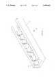
- FIG. 1is a perspective view of a circuit card 12 in a card guide 18 according to the present invention.
- FIG. 2is a perspective view of the preferred embodiment of a card guide 22 according to the present invention.
- FIG. 3is a top view of the preferred embodiment of a card guide 30 according to the present invention.
- FIG. 1is a perspective view of a circuit card 12 in a card guide 18 according to the present invention.
- Circuit card 12includes a connector 14 having a plurality of receptacles of which receptacle 16 is typical. Each receptacle engages a pin on a mating connector which is typically affixed to a backplane. To simplify the drawing, the mating connector and backplane have been omitted. For the purposes of this discussion, it is sufficient to note that the number of pins and receptacles can be quite large. As a result, the accuracy with which the connectors are brought together when connector 14 on circuit card 12 engages the mating connector must be very high. If the connectors are not properly aligned, the pins on the mating connector may be damaged.
- Card guide 18serves to align the two connectors.
- the connectorsare engaged by sliding circuit card 12 through the slot 19 in card guide 18 in the direction shown by arrow 20.
- two card guidesare typically used, one on the top of circuit card 12 and one on the bottom. To simplify the drawing, the top card guide has been omitted.
- the degree to which circuit card 12 can move perpendicular to slot 19 in card guide 18determines the accuracy with which the connectors are mated.
- the perpendicular directionis indicated by the arrows shown at 21.
- slot 19provide a channel whose width is essentially the same as the thickness of circuit card 12. However, if the width of slot 19 exactly matches the thickness of circuit card 18, variations in the thickness of circuit card 18 would lead to circuit card 12 binding in slot 19 as circuit card 12 is inserted therein.
- Card guide 18also provides a means for making electrical connections between a plated region 17 on circuit card 12 and the ground bus on the motherboard. As the frequency of operation of the electronics housed on circuit card 12 increases, the need for better ground connections also increases.
- One method for providing such ground connectionsutilizes spring loaded electrically conducting contacts in the card guide.
- FIG. 2is a perspective view of the preferred embodiment of a card guide 22 according to the present invention.
- Card guide 22is constructed from a channel 2-.
- Card guide 22includes a plurality of resilient protuberances of which protuberance 24 is typical. Two types of protuberances are utilized. The first type of protuberances define a channel having a width substantially the same as the thickness of the circuit card. The second type of protuberances provide the electrical contacts described above.
- the protuberancespreferably consist of spring fingers constructed from stainless steel or a beryllium copper alloy. While the two types of protuberances shown in FIG. 2 appear similar in shape, it will be apparent to those skilled in the art that different shapes may be used for the first and second types of protuberances.
- FIG. 3is a top view of the preferred embodiment of a card guide 30 according to the present invention.
- Card guide 30includes two types of spring fingers, 32 and 34. In the preferred embodiment of the present invention, these fingers are disposed in opposing pairs along the sides of the slot 33 in card guide 30.
- Spring fingers 34provide positioning accuracy for the circuit card.
- the distance 38 between the opposing spring fingersis substantially the same as the thickness of the circuit card.
- the spring constant of spring fingers 34is sufficiently large to prevent the circuit card from moving a substantial distance perpendicular to slot 33. However, the spring constant is small enough to allow sufficient motion to accommodate small irregularities in the the circuit card.
- Spring fingers 32provide electrical connections to the circuit card.
- the distance between opposing spring fingers 32is less than the thickness of the circuit card when no circuit card is inserted in slot 33.
- spring fingers 32are forced apart, thereby creating a spring force engaging each spring finger with the surface of the circuit card.
- the spring constant of spring fingers 32is less than that of spring fingers 34 but sufficient to provide enough force to assure good electrical connection between each spring finger 32 and the circuit card.
- the key feature of the present inventionis the use of two different types of resilient protuberances.
- the first typeis positioned so as to create a channel having a width substantially equal to that of the circuit card and resists motion of the circuit card perpendicular to that channel with a first force.
- the second typeis positioned so as to be forced in a direction perpendicular to the channel when the circuit card is inserted in the channel.
- the second typeexerts a second force on the circuit board which is sufficient to provide electrical contact between the protuberance and the circuit board when the circuit board is inserted in the channel.
- the magnitude of the second forceis less than that of the first force.
- Card guides employing pairs of oppositely disposed spring fingers to both position and provide electrical contactare known to the prior art. However, these designs are unsatisfactory because of the use of the same type of protuberance for both positioning and contact functions.
- Such prior art designswould be equivalent to an embodiment of the present invention in which only spring fingers 34 were utilized and in which the distance between the spring fingers was less than the thickness of the circuit card.
- the spring forcesmust be large so that the defined channel has a width essentially equal to the thickness of the circuit card when the circuit card is inserted in the card guide.
- the channel widthmust be less than the thickness of the circuit card.
- prior art designsare forced to use a channel width which is less than thickness of the circuit card. When a circuit card is inserted in such a card guide, sufficient force must applied to the card to separate the spring fingers. This force has been found to be so high as to cause damage to the circuit card upon insertion or removal from these prior art card guides.
- the present inventionavoids these high forces since the spring fingers used for positioning are only forced apart in response to irregularities in the circuit.
- the electrical contactsare provided by spring fingers having relatively small spring constants. These fingers do not exert high forces on the circuit card even when these fingers are forced apart.
- the protuberances that define the channel for positioning the circuit cardmay be disposed in any manner which defines a channel having a width substantially equal to the thickness of the circuit card.
- the protuberancescould be positioned entirely on one side of the circuit card.
- the wall of channel 21 shown in FIG. 2would define the other wall of the channel through which the circuit card slides.
- the degree to which this channel may deviate from the circuit card widthis determined by the tolerances with which the connector on the circuit card can be mis-positioned with respect to its mating connector on the backplane.
- the connectorsIn general, the connectors must be positioned with respect to each other to within some predetermined accuracy.
- the channel defined by the first protuberancesmust provide this positioning accuracy.
Landscapes
- Coupling Device And Connection With Printed Circuit (AREA)
- Details Of Connecting Devices For Male And Female Coupling (AREA)
Abstract
Description
The present invention relates to electrical equipment in which printed circuit cards are connected to a backplane, and more particularly, to an improved card guide for aligning the circuit card during insertion and for providing ground connections to said circuit card.
Electrical apparatuses often include optional accessories which are provided on a plug-in circuit card and attached to the apparatus by inserting the card into a connector on a motherboard within the apparatus. For example, many computer designs have processor and, or memory boards and the like which are connected to the computer by insertion into a connector on a motherboard.
Connections between the card and motherboard are made by mating a connector on the card to a corresponding connector on the motherboard. As circuit complexity increases, the number and density of pins and sockets on the connectors increases. As the density increases, the accuracy with which the card must be positioned relative to the connector on the motherboard also increases. To provide this accuracy, card guides are normally positioned relative to the connector on the motherboard. The circuit card slides in the card guide which provides the proper alignment during card insertion.
The card guides are also used for providing additional ground connections. Typically, the edge of the circuit card that slides in the guide has a plated section which is connected to the ground bus on the circuit card. Spring loaded protrusions on the card guide engage this plated section. The protrusions in question are connected to the ground bus of the motherboard.
In prior art designs, the card guide utilizes the same set of protrusions both for positioning the card relative to the motherboard and for making the ground connections. To provide sufficient accuracy in aligning the circuit card, the card guide must present a substantially rigid "slot" to the circuit card. The slot must have a width which is very close to the thickness of the circuit card. However, to provide the electrical connections described above, the protrusions must contact the card with sufficient force to assure a good electrical connection.
To accomplish both of these goals, prior art devices have employed spring loaded protrusions disposed on each side of the slot. The protrusions are designed such that the spacing between opposing protrusions is less than the thickness of the circuit card when no circuit card is inserted in the slot. When the circuit card is inserted in the slot, the protrusions are forced apart by the insertion motion. The circuit card is then caused to slide between the protrusions until the connectors are engaged.
Since the protrusions must restrict the lateral motion of the circuit card relative to the slot, the force generated by the protrusions on the sides of the circuit card must be sufficient to prevent the circuit card from moving in a lateral direction. Such a force is significantly greater than the force needed to assure electrical contact between the protrusions and the plated region on the circuit card. In fact, the force required to make prior art card guides function properly is so large, that it hampers the insertion and removal of the circuit cards.
Broadly, it is the object of the present invention to provide an improved printed circuit card guide.
It is a further object of the present invention to provide a circuit card guide having reduced insertion force than prior art devices while providing ground connections for the circuitry on the card.
These and other objects of the present invention will be apparent to those skilled in the art from the following detailed description of the invention and the accompanying drawings.
The present invention comprises a channel guide for positioning a circuit card which engages the card guide along an edge thereof, the edge of said circuit card having a predetermined thickness. The channel guide includes a means for defining a first channel having left and right walls and a width greater than said predetermined thickness. A plurality of first resilient protuberances are positioned along at least one of said left and right walls. The first protuberances define a second channel having a width substantially equal to said predetermined thickness. A second resilient electrically conducting protuberance is positioned along one of said left and right walls. The second protuberance is positioned such that said protuberance is forced toward the wall on which said protuberance is positioned when said circuit card is inserted into said channel guide.
FIG. 1 is a perspective view of acircuit card 12 in acard guide 18 according to the present invention.
FIG. 2 is a perspective view of the preferred embodiment of acard guide 22 according to the present invention.
FIG. 3 is a top view of the preferred embodiment of acard guide 30 according to the present invention.
The manner in which the present invention provides its advantages may be more easily understood with reference to FIG. 1 which is a perspective view of acircuit card 12 in acard guide 18 according to the present invention.Circuit card 12 includes aconnector 14 having a plurality of receptacles of whichreceptacle 16 is typical. Each receptacle engages a pin on a mating connector which is typically affixed to a backplane. To simplify the drawing, the mating connector and backplane have been omitted. For the purposes of this discussion, it is sufficient to note that the number of pins and receptacles can be quite large. As a result, the accuracy with which the connectors are brought together whenconnector 14 oncircuit card 12 engages the mating connector must be very high. If the connectors are not properly aligned, the pins on the mating connector may be damaged.
The manner in which the alignment and electrical connections are provided by a card guide according to the present invention may be more easily understood with reference to FIG. 2 which is a perspective view of the preferred embodiment of acard guide 22 according to the present invention.Card guide 22 is constructed from a channel 2-.Card guide 22 includes a plurality of resilient protuberances of whichprotuberance 24 is typical. Two types of protuberances are utilized. The first type of protuberances define a channel having a width substantially the same as the thickness of the circuit card. The second type of protuberances provide the electrical contacts described above. The protuberances preferably consist of spring fingers constructed from stainless steel or a beryllium copper alloy. While the two types of protuberances shown in FIG. 2 appear similar in shape, it will be apparent to those skilled in the art that different shapes may be used for the first and second types of protuberances.
The manner in which these protuberances provide the above described functionality may be better understood with reference to FIG. 3 which is a top view of the preferred embodiment of acard guide 30 according to the present invention.Card guide 30 includes two types of spring fingers, 32 and 34. In the preferred embodiment of the present invention, these fingers are disposed in opposing pairs along the sides of theslot 33 incard guide 30.Spring fingers 34 provide positioning accuracy for the circuit card. Thedistance 38 between the opposing spring fingers is substantially the same as the thickness of the circuit card. The spring constant ofspring fingers 34 is sufficiently large to prevent the circuit card from moving a substantial distance perpendicular to slot 33. However, the spring constant is small enough to allow sufficient motion to accommodate small irregularities in the the circuit card.
While the above description of a card guide according to the present invention utilized oppositely disposed pairs of spring fingers, it will be apparent to those skilled in the art that the present invention may be constructed from non-opposed pairs of spring fingers. The key feature of the present invention is the use of two different types of resilient protuberances. The first type is positioned so as to create a channel having a width substantially equal to that of the circuit card and resists motion of the circuit card perpendicular to that channel with a first force. The second type is positioned so as to be forced in a direction perpendicular to the channel when the circuit card is inserted in the channel. The second type exerts a second force on the circuit board which is sufficient to provide electrical contact between the protuberance and the circuit board when the circuit board is inserted in the channel. The magnitude of the second force is less than that of the first force.
Card guides employing pairs of oppositely disposed spring fingers to both position and provide electrical contact are known to the prior art. However, these designs are unsatisfactory because of the use of the same type of protuberance for both positioning and contact functions. Such prior art designs would be equivalent to an embodiment of the present invention in which only springfingers 34 were utilized and in which the distance between the spring fingers was less than the thickness of the circuit card. For proper positioning, the spring forces must be large so that the defined channel has a width essentially equal to the thickness of the circuit card when the circuit card is inserted in the card guide. To provide the electrical contact function, the channel width must be less than the thickness of the circuit card. Hence, prior art designs are forced to use a channel width which is less than thickness of the circuit card. When a circuit card is inserted in such a card guide, sufficient force must applied to the card to separate the spring fingers. This force has been found to be so high as to cause damage to the circuit card upon insertion or removal from these prior art card guides.
The present invention avoids these high forces since the spring fingers used for positioning are only forced apart in response to irregularities in the circuit. The electrical contacts are provided by spring fingers having relatively small spring constants. These fingers do not exert high forces on the circuit card even when these fingers are forced apart.
While the above described embodiments of the present invention have utilized protuberances which were positioned in opposing pairs, it will be apparent to those skilled in the art that the use of opposing pairs is not essential to practice of the present invention. The protuberances that define the channel for positioning the circuit card may be disposed in any manner which defines a channel having a width substantially equal to the thickness of the circuit card. For example, the protuberances could be positioned entirely on one side of the circuit card. In this case, the wall ofchannel 21 shown in FIG. 2 would define the other wall of the channel through which the circuit card slides.
The degree to which this channel may deviate from the circuit card width is determined by the tolerances with which the connector on the circuit card can be mis-positioned with respect to its mating connector on the backplane. In general, the connectors must be positioned with respect to each other to within some predetermined accuracy. The channel defined by the first protuberances must provide this positioning accuracy.
Similarly, embodiments in which the second type of protuberance is only present on one side of the circuit card will be apparent to those skilled in the art. In principle, a single protuberance of the second type could be positioned such that the insertion of the card into the card guide forced said protuberance toward the wall of the channel on which it was positioned with sufficient force to provide a good electrical contact.
There has been described herein a card guide. Various modifications to the present invention will become apparent to those skilled in the art from the foregoing description and accompanying drawings. Accordingly, the present invention is to be limited solely by the scope of the following claims.
Claims (4)
1. A card guide for positioning a circuit card, said circuit card engaging said card guide along an edge thereof, said edge having a predetermined thickness, said card guide comprising:
means for defining a first channel having left and right walls and a width greater than said predetermined thickness;
a plurality of first resilient protuberances positioned along at least one of said left and right walls, said first protuberances defining a second channel having a width substantially equal to said predetermined thickness; and
a second resilient electrically conducting protuberance positioned along one of said left and right walls, said second protuberance being positioned such that said protuberance is forced toward said wall on which said protuberance is positioned when said circuit card is inserted into said card guide.
2. The card guide of claim 1 wherein said first protuberances are positioned in opposing pairs, one member of each said pair being positioned on said right wall and the other member of each said pair being positioned on said left wall.
3. The card guide of claim 2 wherein said first protuberances comprise metallic springs having first spring constants, the distance between the members of said opposing pairs being substantially equal to the thickness of said circuit card.
4. The card guide of claim 3 wherein said second protuberance comprises a metallic spring having spring constant less than said spring constants of said first protuberances and being positioned such that said metallic spring engages said circuit card with a predetermined force when said circuit card is inserted in said card guide.
Priority Applications (1)
| Application Number | Priority Date | Filing Date | Title |
|---|---|---|---|
| US07/573,638US5055061A (en) | 1990-08-27 | 1990-08-27 | Circuit card guide |
Applications Claiming Priority (1)
| Application Number | Priority Date | Filing Date | Title |
|---|---|---|---|
| US07/573,638US5055061A (en) | 1990-08-27 | 1990-08-27 | Circuit card guide |
Publications (1)
| Publication Number | Publication Date |
|---|---|
| US5055061Atrue US5055061A (en) | 1991-10-08 |
Family
ID=24292802
Family Applications (1)
| Application Number | Title | Priority Date | Filing Date |
|---|---|---|---|
| US07/573,638Expired - LifetimeUS5055061A (en) | 1990-08-27 | 1990-08-27 | Circuit card guide |
Country Status (1)
| Country | Link |
|---|---|
| US (1) | US5055061A (en) |
Cited By (27)
| Publication number | Priority date | Publication date | Assignee | Title |
|---|---|---|---|---|
| US5402319A (en)* | 1993-04-22 | 1995-03-28 | Rockwell International Corporation | Avionics line replaceable unit with frameless spring ramp circuit card retainer |
| US5467254A (en)* | 1993-11-04 | 1995-11-14 | Synoptics Communications, Inc. | Supportive guide for circuit-card grounding including tracks having staggered protrusions at the proximal end of the tracks |
| US5682299A (en)* | 1995-06-06 | 1997-10-28 | Norand Corporation | PCMCIA module having multiple point grounding |
| US5711677A (en)* | 1996-01-11 | 1998-01-27 | Hewlett-Packard Company | Multi-functional I/O card guide |
| US5963681A (en)* | 1997-08-29 | 1999-10-05 | Hewlett-Packard Company | Circuit board guide and light conduit |
| US5991158A (en)* | 1995-05-24 | 1999-11-23 | Dell Usa, L.P. | Slot for mechanically detecting the presence of a computer card |
| US6017246A (en)* | 1996-06-10 | 2000-01-25 | Matsushita Electric Industrial Co., Ltd. | Printed wiring board |
| US6304456B1 (en)* | 1999-07-22 | 2001-10-16 | Hewlett-Packard Company | Housing assembly having simplified circuit board assembly, retention, and electrical connection features |
| US6309237B1 (en)* | 1999-03-22 | 2001-10-30 | Tyco Electronics Logistics Ag | System with printed circuit boards that can be plugged together |
| US6346003B1 (en)* | 1999-02-22 | 2002-02-12 | Bivar | Circuit card guide having a grounding strip |
| US6580616B2 (en) | 2001-10-16 | 2003-06-17 | Hewlett-Packard Company | Multiple circuit board adapter |
| US20040047119A1 (en)* | 2001-08-22 | 2004-03-11 | Michael Wortman | Housing assembly having simplified circuit board assembly, retention, and electrical connection features |
| US6728114B2 (en)* | 2002-07-05 | 2004-04-27 | Alcatel Canada Inc. | Space-saving card guides for card cage and method of installing same on a card cage or frame |
| US6735093B2 (en)* | 2000-08-12 | 2004-05-11 | Wistron Corporation | Computer system and EMI structure thereof |
| US6821141B1 (en)* | 2003-06-25 | 2004-11-23 | Tatung Co., Ltd. | Sliding track assembly for mobile PC board |
| US20050018389A1 (en)* | 2003-07-24 | 2005-01-27 | International Business Machines Corporation | Alignment docking system |
| US20090191726A1 (en)* | 2008-01-30 | 2009-07-30 | Samsung Electronics Co., Ltd. | Connecting device and method for electronic machinery |
| US20100258518A1 (en)* | 2009-04-13 | 2010-10-14 | Curtis Matthew Yeoman | Slip on rail system |
| US20120104207A1 (en)* | 2010-10-28 | 2012-05-03 | Hon Hai Precision Industry Co., Ltd. | Test bracket for circuit board |
| US20120244741A1 (en)* | 2009-12-15 | 2012-09-27 | Chin Hua Lim | Connector |
| US20130265675A1 (en)* | 2012-04-09 | 2013-10-10 | Lsis Co., Ltd. | Digital protective relay |
| US8724336B2 (en) | 2010-07-02 | 2014-05-13 | National Instruments Corporation | Card guide system and method |
| US20150055304A1 (en)* | 2013-08-26 | 2015-02-26 | Wistron Corporation | Electronic device |
| US20190334264A1 (en)* | 2018-04-25 | 2019-10-31 | Fanuc Corporation | Electronic device |
| US10595429B2 (en)* | 2018-04-10 | 2020-03-17 | Fanuc Corporation | Electronic device |
| US11455019B2 (en)* | 2020-08-19 | 2022-09-27 | Quanta Computer Inc. | Docking system having elastic rail portions |
| US20220391604A1 (en)* | 2021-06-04 | 2022-12-08 | Hitachi Channel Solutions, Corp. | Card reader and foreign object detection method for card reader |
Citations (4)
| Publication number | Priority date | Publication date | Assignee | Title |
|---|---|---|---|---|
| US3231785A (en)* | 1963-08-12 | 1966-01-25 | Anthony D Calabro | Circuit board mounting device |
| US3950057A (en)* | 1975-06-02 | 1976-04-13 | Calabro Anthony Denis | Composite printed circuit card guide and holding device |
| US4019099A (en)* | 1976-01-15 | 1977-04-19 | Calabro Anthony Denis | Circuit board mounting device |
| US4214292A (en)* | 1978-11-30 | 1980-07-22 | Sperry Corporation | Printed circuit board guide spring |
- 1990
- 1990-08-27USUS07/573,638patent/US5055061A/ennot_activeExpired - Lifetime
Patent Citations (4)
| Publication number | Priority date | Publication date | Assignee | Title |
|---|---|---|---|---|
| US3231785A (en)* | 1963-08-12 | 1966-01-25 | Anthony D Calabro | Circuit board mounting device |
| US3950057A (en)* | 1975-06-02 | 1976-04-13 | Calabro Anthony Denis | Composite printed circuit card guide and holding device |
| US4019099A (en)* | 1976-01-15 | 1977-04-19 | Calabro Anthony Denis | Circuit board mounting device |
| US4214292A (en)* | 1978-11-30 | 1980-07-22 | Sperry Corporation | Printed circuit board guide spring |
Cited By (32)
| Publication number | Priority date | Publication date | Assignee | Title |
|---|---|---|---|---|
| US5402319A (en)* | 1993-04-22 | 1995-03-28 | Rockwell International Corporation | Avionics line replaceable unit with frameless spring ramp circuit card retainer |
| US5467254A (en)* | 1993-11-04 | 1995-11-14 | Synoptics Communications, Inc. | Supportive guide for circuit-card grounding including tracks having staggered protrusions at the proximal end of the tracks |
| US5991158A (en)* | 1995-05-24 | 1999-11-23 | Dell Usa, L.P. | Slot for mechanically detecting the presence of a computer card |
| US5682299A (en)* | 1995-06-06 | 1997-10-28 | Norand Corporation | PCMCIA module having multiple point grounding |
| US5711677A (en)* | 1996-01-11 | 1998-01-27 | Hewlett-Packard Company | Multi-functional I/O card guide |
| US6017246A (en)* | 1996-06-10 | 2000-01-25 | Matsushita Electric Industrial Co., Ltd. | Printed wiring board |
| US5963681A (en)* | 1997-08-29 | 1999-10-05 | Hewlett-Packard Company | Circuit board guide and light conduit |
| US6346003B1 (en)* | 1999-02-22 | 2002-02-12 | Bivar | Circuit card guide having a grounding strip |
| US6309237B1 (en)* | 1999-03-22 | 2001-10-30 | Tyco Electronics Logistics Ag | System with printed circuit boards that can be plugged together |
| US6304456B1 (en)* | 1999-07-22 | 2001-10-16 | Hewlett-Packard Company | Housing assembly having simplified circuit board assembly, retention, and electrical connection features |
| US6735093B2 (en)* | 2000-08-12 | 2004-05-11 | Wistron Corporation | Computer system and EMI structure thereof |
| US6940726B2 (en)* | 2001-08-22 | 2005-09-06 | Hewlett-Packard Development Company, L.P. | Housing assembly having simplified circuit board assembly, retention, and electrical connection features |
| US20040047119A1 (en)* | 2001-08-22 | 2004-03-11 | Michael Wortman | Housing assembly having simplified circuit board assembly, retention, and electrical connection features |
| US6580616B2 (en) | 2001-10-16 | 2003-06-17 | Hewlett-Packard Company | Multiple circuit board adapter |
| US6728114B2 (en)* | 2002-07-05 | 2004-04-27 | Alcatel Canada Inc. | Space-saving card guides for card cage and method of installing same on a card cage or frame |
| US6821141B1 (en)* | 2003-06-25 | 2004-11-23 | Tatung Co., Ltd. | Sliding track assembly for mobile PC board |
| US20050018389A1 (en)* | 2003-07-24 | 2005-01-27 | International Business Machines Corporation | Alignment docking system |
| US6950301B2 (en) | 2003-07-24 | 2005-09-27 | International Business Machines Corporation | Alignment docking system |
| US20090191726A1 (en)* | 2008-01-30 | 2009-07-30 | Samsung Electronics Co., Ltd. | Connecting device and method for electronic machinery |
| US20100258518A1 (en)* | 2009-04-13 | 2010-10-14 | Curtis Matthew Yeoman | Slip on rail system |
| US20120244741A1 (en)* | 2009-12-15 | 2012-09-27 | Chin Hua Lim | Connector |
| US8585428B2 (en)* | 2009-12-15 | 2013-11-19 | 3M Innovative Properties Company | Connector |
| US8724336B2 (en) | 2010-07-02 | 2014-05-13 | National Instruments Corporation | Card guide system and method |
| US20120104207A1 (en)* | 2010-10-28 | 2012-05-03 | Hon Hai Precision Industry Co., Ltd. | Test bracket for circuit board |
| US20130265675A1 (en)* | 2012-04-09 | 2013-10-10 | Lsis Co., Ltd. | Digital protective relay |
| US9099865B2 (en)* | 2012-04-09 | 2015-08-04 | Lsis Co., Ltd. | Digital protective relay |
| US20150055304A1 (en)* | 2013-08-26 | 2015-02-26 | Wistron Corporation | Electronic device |
| US10595429B2 (en)* | 2018-04-10 | 2020-03-17 | Fanuc Corporation | Electronic device |
| US20190334264A1 (en)* | 2018-04-25 | 2019-10-31 | Fanuc Corporation | Electronic device |
| US11455019B2 (en)* | 2020-08-19 | 2022-09-27 | Quanta Computer Inc. | Docking system having elastic rail portions |
| US20220391604A1 (en)* | 2021-06-04 | 2022-12-08 | Hitachi Channel Solutions, Corp. | Card reader and foreign object detection method for card reader |
| US11710004B2 (en)* | 2021-06-04 | 2023-07-25 | Hitachi Channel Solutions, Corp. | Card reader and foreign object detection method for card reader |
Similar Documents
| Publication | Publication Date | Title |
|---|---|---|
| US5055061A (en) | Circuit card guide | |
| US4780603A (en) | Integrated circuit card and connector arrangement using same | |
| US6229709B1 (en) | Printed circuit board card guide | |
| US3966290A (en) | Polarized connector | |
| EP0485196A2 (en) | Optical connection to backplanes | |
| EP0349133A1 (en) | Extraction tool | |
| EP0317467A2 (en) | Plugable assembly for printed circuit cards | |
| US5755592A (en) | Combined ground strap and board lock for electrical connector assembly | |
| EP0130556A1 (en) | Zero insertion force connector-card retention and polarization device | |
| US6373712B1 (en) | Device for inserting circuit cards into electrical machines | |
| GB2142783A (en) | Cage apparatus for printed circuit boards and method for preventing sharp spikes in the signal applied to said printed circuit boards | |
| WO1994019844A1 (en) | Circuit card interface system | |
| US7258574B2 (en) | Snap-fit electromagnetic shield | |
| US5443398A (en) | Inverse backplane connector system | |
| US6520783B2 (en) | Electrical card connector having polarization mechanism | |
| US20060148318A1 (en) | Electrical card connector | |
| US5317480A (en) | Circuit pack interconnection | |
| EP0370373B1 (en) | Printed circuit card guide | |
| US5283713A (en) | Injector/ejector system for a plug-in module and apparatus using the systems | |
| US6567274B1 (en) | Faceplate | |
| EP0505576B1 (en) | Apparatus for connecting tentatively electronic circuit unit | |
| EP1054480A2 (en) | Electromagnetic interference shielding gasket | |
| EP0584416A1 (en) | Connector | |
| US7090513B2 (en) | Electrical card connector | |
| US20050287870A1 (en) | Card connector |
Legal Events
| Date | Code | Title | Description |
|---|---|---|---|
| AS | Assignment | Owner name:HEWLETT-PACKARD COMPANY, A CORP OF CA, CALIFORNIA Free format text:ASSIGNMENT OF ASSIGNORS INTEREST.;ASSIGNOR:LICHTENWALTER, GUY;REEL/FRAME:005426/0925 Effective date:19900823 | |
| STCF | Information on status: patent grant | Free format text:PATENTED CASE | |
| FEPP | Fee payment procedure | Free format text:PAYOR NUMBER ASSIGNED (ORIGINAL EVENT CODE: ASPN); ENTITY STATUS OF PATENT OWNER: LARGE ENTITY | |
| FPAY | Fee payment | Year of fee payment:4 | |
| FPAY | Fee payment | Year of fee payment:8 | |
| AS | Assignment | Owner name:HEWLETT-PACKARD COMPANY, COLORADO Free format text:MERGER;ASSIGNOR:HEWLETT-PACKARD COMPANY;REEL/FRAME:011523/0469 Effective date:19980520 | |
| FPAY | Fee payment | Year of fee payment:12 |