US5053357A - Method of aligning and mounting an electronic device on a printed circuit board using a flexible substrate having fixed lead arrays thereon - Google Patents
Method of aligning and mounting an electronic device on a printed circuit board using a flexible substrate having fixed lead arrays thereonDownload PDFInfo
- Publication number
- US5053357A US5053357AUS07/567,838US56783890AUS5053357AUS 5053357 AUS5053357 AUS 5053357AUS 56783890 AUS56783890 AUS 56783890AUS 5053357 AUS5053357 AUS 5053357A
- Authority
- US
- United States
- Prior art keywords
- traces
- pcb
- substrate
- electronic component
- bonding areas
- Prior art date
- Legal status (The legal status is an assumption and is not a legal conclusion. Google has not performed a legal analysis and makes no representation as to the accuracy of the status listed.)
- Expired - Lifetime
Links
Images


Classifications
- H—ELECTRICITY
- H01—ELECTRIC ELEMENTS
- H01L—SEMICONDUCTOR DEVICES NOT COVERED BY CLASS H10
- H01L22/00—Testing or measuring during manufacture or treatment; Reliability measurements, i.e. testing of parts without further processing to modify the parts as such; Structural arrangements therefor
- H—ELECTRICITY
- H01—ELECTRIC ELEMENTS
- H01L—SEMICONDUCTOR DEVICES NOT COVERED BY CLASS H10
- H01L23/00—Details of semiconductor or other solid state devices
- H01L23/28—Encapsulations, e.g. encapsulating layers, coatings, e.g. for protection
- H01L23/31—Encapsulations, e.g. encapsulating layers, coatings, e.g. for protection characterised by the arrangement or shape
- H01L23/3107—Encapsulations, e.g. encapsulating layers, coatings, e.g. for protection characterised by the arrangement or shape the device being completely enclosed
- H01L23/3121—Encapsulations, e.g. encapsulating layers, coatings, e.g. for protection characterised by the arrangement or shape the device being completely enclosed a substrate forming part of the encapsulation
- H—ELECTRICITY
- H01—ELECTRIC ELEMENTS
- H01L—SEMICONDUCTOR DEVICES NOT COVERED BY CLASS H10
- H01L23/00—Details of semiconductor or other solid state devices
- H01L23/48—Arrangements for conducting electric current to or from the solid state body in operation, e.g. leads, terminal arrangements ; Selection of materials therefor
- H01L23/488—Arrangements for conducting electric current to or from the solid state body in operation, e.g. leads, terminal arrangements ; Selection of materials therefor consisting of soldered or bonded constructions
- H01L23/498—Leads, i.e. metallisations or lead-frames on insulating substrates, e.g. chip carriers
- H01L23/4985—Flexible insulating substrates
- H—ELECTRICITY
- H05—ELECTRIC TECHNIQUES NOT OTHERWISE PROVIDED FOR
- H05K—PRINTED CIRCUITS; CASINGS OR CONSTRUCTIONAL DETAILS OF ELECTRIC APPARATUS; MANUFACTURE OF ASSEMBLAGES OF ELECTRICAL COMPONENTS
- H05K3/00—Apparatus or processes for manufacturing printed circuits
- H05K3/30—Assembling printed circuits with electric components, e.g. with resistor
- H05K3/303—Surface mounted components, e.g. affixing before soldering, aligning means, spacing means
- H—ELECTRICITY
- H01—ELECTRIC ELEMENTS
- H01L—SEMICONDUCTOR DEVICES NOT COVERED BY CLASS H10
- H01L2224/00—Indexing scheme for arrangements for connecting or disconnecting semiconductor or solid-state bodies and methods related thereto as covered by H01L24/00
- H01L2224/01—Means for bonding being attached to, or being formed on, the surface to be connected, e.g. chip-to-package, die-attach, "first-level" interconnects; Manufacturing methods related thereto
- H01L2224/02—Bonding areas; Manufacturing methods related thereto
- H01L2224/04—Structure, shape, material or disposition of the bonding areas prior to the connecting process
- H01L2224/05—Structure, shape, material or disposition of the bonding areas prior to the connecting process of an individual bonding area
- H01L2224/0554—External layer
- H01L2224/0555—Shape
- H01L2224/05552—Shape in top view
- H01L2224/05554—Shape in top view being square
- H—ELECTRICITY
- H01—ELECTRIC ELEMENTS
- H01L—SEMICONDUCTOR DEVICES NOT COVERED BY CLASS H10
- H01L2224/00—Indexing scheme for arrangements for connecting or disconnecting semiconductor or solid-state bodies and methods related thereto as covered by H01L24/00
- H01L2224/01—Means for bonding being attached to, or being formed on, the surface to be connected, e.g. chip-to-package, die-attach, "first-level" interconnects; Manufacturing methods related thereto
- H01L2224/26—Layer connectors, e.g. plate connectors, solder or adhesive layers; Manufacturing methods related thereto
- H01L2224/31—Structure, shape, material or disposition of the layer connectors after the connecting process
- H01L2224/32—Structure, shape, material or disposition of the layer connectors after the connecting process of an individual layer connector
- H01L2224/321—Disposition
- H01L2224/32151—Disposition the layer connector connecting between a semiconductor or solid-state body and an item not being a semiconductor or solid-state body, e.g. chip-to-substrate, chip-to-passive
- H01L2224/32221—Disposition the layer connector connecting between a semiconductor or solid-state body and an item not being a semiconductor or solid-state body, e.g. chip-to-substrate, chip-to-passive the body and the item being stacked
- H01L2224/32225—Disposition the layer connector connecting between a semiconductor or solid-state body and an item not being a semiconductor or solid-state body, e.g. chip-to-substrate, chip-to-passive the body and the item being stacked the item being non-metallic, e.g. insulating substrate with or without metallisation
- H—ELECTRICITY
- H01—ELECTRIC ELEMENTS
- H01L—SEMICONDUCTOR DEVICES NOT COVERED BY CLASS H10
- H01L2224/00—Indexing scheme for arrangements for connecting or disconnecting semiconductor or solid-state bodies and methods related thereto as covered by H01L24/00
- H01L2224/01—Means for bonding being attached to, or being formed on, the surface to be connected, e.g. chip-to-package, die-attach, "first-level" interconnects; Manufacturing methods related thereto
- H01L2224/42—Wire connectors; Manufacturing methods related thereto
- H01L2224/47—Structure, shape, material or disposition of the wire connectors after the connecting process
- H01L2224/48—Structure, shape, material or disposition of the wire connectors after the connecting process of an individual wire connector
- H01L2224/4805—Shape
- H01L2224/4809—Loop shape
- H01L2224/48091—Arched
- H—ELECTRICITY
- H01—ELECTRIC ELEMENTS
- H01L—SEMICONDUCTOR DEVICES NOT COVERED BY CLASS H10
- H01L2224/00—Indexing scheme for arrangements for connecting or disconnecting semiconductor or solid-state bodies and methods related thereto as covered by H01L24/00
- H01L2224/01—Means for bonding being attached to, or being formed on, the surface to be connected, e.g. chip-to-package, die-attach, "first-level" interconnects; Manufacturing methods related thereto
- H01L2224/42—Wire connectors; Manufacturing methods related thereto
- H01L2224/47—Structure, shape, material or disposition of the wire connectors after the connecting process
- H01L2224/48—Structure, shape, material or disposition of the wire connectors after the connecting process of an individual wire connector
- H01L2224/481—Disposition
- H01L2224/48151—Connecting between a semiconductor or solid-state body and an item not being a semiconductor or solid-state body, e.g. chip-to-substrate, chip-to-passive
- H01L2224/48221—Connecting between a semiconductor or solid-state body and an item not being a semiconductor or solid-state body, e.g. chip-to-substrate, chip-to-passive the body and the item being stacked
- H01L2224/48225—Connecting between a semiconductor or solid-state body and an item not being a semiconductor or solid-state body, e.g. chip-to-substrate, chip-to-passive the body and the item being stacked the item being non-metallic, e.g. insulating substrate with or without metallisation
- H01L2224/48227—Connecting between a semiconductor or solid-state body and an item not being a semiconductor or solid-state body, e.g. chip-to-substrate, chip-to-passive the body and the item being stacked the item being non-metallic, e.g. insulating substrate with or without metallisation connecting the wire to a bond pad of the item
- H—ELECTRICITY
- H01—ELECTRIC ELEMENTS
- H01L—SEMICONDUCTOR DEVICES NOT COVERED BY CLASS H10
- H01L2224/00—Indexing scheme for arrangements for connecting or disconnecting semiconductor or solid-state bodies and methods related thereto as covered by H01L24/00
- H01L2224/73—Means for bonding being of different types provided for in two or more of groups H01L2224/10, H01L2224/18, H01L2224/26, H01L2224/34, H01L2224/42, H01L2224/50, H01L2224/63, H01L2224/71
- H01L2224/732—Location after the connecting process
- H01L2224/73251—Location after the connecting process on different surfaces
- H01L2224/73265—Layer and wire connectors
- H—ELECTRICITY
- H01—ELECTRIC ELEMENTS
- H01L—SEMICONDUCTOR DEVICES NOT COVERED BY CLASS H10
- H01L24/00—Arrangements for connecting or disconnecting semiconductor or solid-state bodies; Methods or apparatus related thereto
- H01L24/01—Means for bonding being attached to, or being formed on, the surface to be connected, e.g. chip-to-package, die-attach, "first-level" interconnects; Manufacturing methods related thereto
- H01L24/42—Wire connectors; Manufacturing methods related thereto
- H01L24/47—Structure, shape, material or disposition of the wire connectors after the connecting process
- H01L24/48—Structure, shape, material or disposition of the wire connectors after the connecting process of an individual wire connector
- H—ELECTRICITY
- H01—ELECTRIC ELEMENTS
- H01L—SEMICONDUCTOR DEVICES NOT COVERED BY CLASS H10
- H01L24/00—Arrangements for connecting or disconnecting semiconductor or solid-state bodies; Methods or apparatus related thereto
- H01L24/73—Means for bonding being of different types provided for in two or more of groups H01L24/10, H01L24/18, H01L24/26, H01L24/34, H01L24/42, H01L24/50, H01L24/63, H01L24/71
- H—ELECTRICITY
- H01—ELECTRIC ELEMENTS
- H01L—SEMICONDUCTOR DEVICES NOT COVERED BY CLASS H10
- H01L2924/00—Indexing scheme for arrangements or methods for connecting or disconnecting semiconductor or solid-state bodies as covered by H01L24/00
- H01L2924/0001—Technical content checked by a classifier
- H01L2924/00014—Technical content checked by a classifier the subject-matter covered by the group, the symbol of which is combined with the symbol of this group, being disclosed without further technical details
- H—ELECTRICITY
- H01—ELECTRIC ELEMENTS
- H01L—SEMICONDUCTOR DEVICES NOT COVERED BY CLASS H10
- H01L2924/00—Indexing scheme for arrangements or methods for connecting or disconnecting semiconductor or solid-state bodies as covered by H01L24/00
- H01L2924/01—Chemical elements
- H01L2924/01078—Platinum [Pt]
- H—ELECTRICITY
- H01—ELECTRIC ELEMENTS
- H01L—SEMICONDUCTOR DEVICES NOT COVERED BY CLASS H10
- H01L2924/00—Indexing scheme for arrangements or methods for connecting or disconnecting semiconductor or solid-state bodies as covered by H01L24/00
- H01L2924/01—Chemical elements
- H01L2924/01079—Gold [Au]
- H—ELECTRICITY
- H01—ELECTRIC ELEMENTS
- H01L—SEMICONDUCTOR DEVICES NOT COVERED BY CLASS H10
- H01L2924/00—Indexing scheme for arrangements or methods for connecting or disconnecting semiconductor or solid-state bodies as covered by H01L24/00
- H01L2924/10—Details of semiconductor or other solid state devices to be connected
- H01L2924/1015—Shape
- H01L2924/1016—Shape being a cuboid
- H01L2924/10162—Shape being a cuboid with a square active surface
- H—ELECTRICITY
- H01—ELECTRIC ELEMENTS
- H01L—SEMICONDUCTOR DEVICES NOT COVERED BY CLASS H10
- H01L2924/00—Indexing scheme for arrangements or methods for connecting or disconnecting semiconductor or solid-state bodies as covered by H01L24/00
- H01L2924/10—Details of semiconductor or other solid state devices to be connected
- H01L2924/11—Device type
- H01L2924/12—Passive devices, e.g. 2 terminal devices
- H01L2924/1204—Optical Diode
- H01L2924/12042—LASER
- H—ELECTRICITY
- H01—ELECTRIC ELEMENTS
- H01L—SEMICONDUCTOR DEVICES NOT COVERED BY CLASS H10
- H01L2924/00—Indexing scheme for arrangements or methods for connecting or disconnecting semiconductor or solid-state bodies as covered by H01L24/00
- H01L2924/10—Details of semiconductor or other solid state devices to be connected
- H01L2924/11—Device type
- H01L2924/14—Integrated circuits
- H—ELECTRICITY
- H01—ELECTRIC ELEMENTS
- H01L—SEMICONDUCTOR DEVICES NOT COVERED BY CLASS H10
- H01L2924/00—Indexing scheme for arrangements or methods for connecting or disconnecting semiconductor or solid-state bodies as covered by H01L24/00
- H01L2924/15—Details of package parts other than the semiconductor or other solid state devices to be connected
- H01L2924/151—Die mounting substrate
- H01L2924/153—Connection portion
- H01L2924/1532—Connection portion the connection portion being formed on the die mounting surface of the substrate
- H—ELECTRICITY
- H01—ELECTRIC ELEMENTS
- H01L—SEMICONDUCTOR DEVICES NOT COVERED BY CLASS H10
- H01L2924/00—Indexing scheme for arrangements or methods for connecting or disconnecting semiconductor or solid-state bodies as covered by H01L24/00
- H01L2924/15—Details of package parts other than the semiconductor or other solid state devices to be connected
- H01L2924/181—Encapsulation
- H—ELECTRICITY
- H05—ELECTRIC TECHNIQUES NOT OTHERWISE PROVIDED FOR
- H05K—PRINTED CIRCUITS; CASINGS OR CONSTRUCTIONAL DETAILS OF ELECTRIC APPARATUS; MANUFACTURE OF ASSEMBLAGES OF ELECTRICAL COMPONENTS
- H05K2201/00—Indexing scheme relating to printed circuits covered by H05K1/00
- H05K2201/10—Details of components or other objects attached to or integrated in a printed circuit board
- H05K2201/10227—Other objects, e.g. metallic pieces
- H05K2201/10295—Metallic connector elements partly mounted in a hole of the PCB
- H05K2201/10303—Pin-in-hole mounted pins
- H—ELECTRICITY
- H05—ELECTRIC TECHNIQUES NOT OTHERWISE PROVIDED FOR
- H05K—PRINTED CIRCUITS; CASINGS OR CONSTRUCTIONAL DETAILS OF ELECTRIC APPARATUS; MANUFACTURE OF ASSEMBLAGES OF ELECTRICAL COMPONENTS
- H05K2201/00—Indexing scheme relating to printed circuits covered by H05K1/00
- H05K2201/10—Details of components or other objects attached to or integrated in a printed circuit board
- H05K2201/10613—Details of electrical connections of non-printed components, e.g. special leads
- H05K2201/10621—Components characterised by their electrical contacts
- H05K2201/10681—Tape Carrier Package [TCP]; Flexible sheet connector
- H—ELECTRICITY
- H05—ELECTRIC TECHNIQUES NOT OTHERWISE PROVIDED FOR
- H05K—PRINTED CIRCUITS; CASINGS OR CONSTRUCTIONAL DETAILS OF ELECTRIC APPARATUS; MANUFACTURE OF ASSEMBLAGES OF ELECTRICAL COMPONENTS
- H05K2203/00—Indexing scheme relating to apparatus or processes for manufacturing printed circuits covered by H05K3/00
- H05K2203/16—Inspection; Monitoring; Aligning
- H05K2203/162—Testing a finished product, e.g. heat cycle testing of solder joints
- H—ELECTRICITY
- H05—ELECTRIC TECHNIQUES NOT OTHERWISE PROVIDED FOR
- H05K—PRINTED CIRCUITS; CASINGS OR CONSTRUCTIONAL DETAILS OF ELECTRIC APPARATUS; MANUFACTURE OF ASSEMBLAGES OF ELECTRICAL COMPONENTS
- H05K2203/00—Indexing scheme relating to apparatus or processes for manufacturing printed circuits covered by H05K3/00
- H05K2203/16—Inspection; Monitoring; Aligning
- H05K2203/167—Using mechanical means for positioning, alignment or registration, e.g. using rod-in-hole alignment
- Y—GENERAL TAGGING OF NEW TECHNOLOGICAL DEVELOPMENTS; GENERAL TAGGING OF CROSS-SECTIONAL TECHNOLOGIES SPANNING OVER SEVERAL SECTIONS OF THE IPC; TECHNICAL SUBJECTS COVERED BY FORMER USPC CROSS-REFERENCE ART COLLECTIONS [XRACs] AND DIGESTS
- Y02—TECHNOLOGIES OR APPLICATIONS FOR MITIGATION OR ADAPTATION AGAINST CLIMATE CHANGE
- Y02P—CLIMATE CHANGE MITIGATION TECHNOLOGIES IN THE PRODUCTION OR PROCESSING OF GOODS
- Y02P70/00—Climate change mitigation technologies in the production process for final industrial or consumer products
- Y02P70/50—Manufacturing or production processes characterised by the final manufactured product
- Y—GENERAL TAGGING OF NEW TECHNOLOGICAL DEVELOPMENTS; GENERAL TAGGING OF CROSS-SECTIONAL TECHNOLOGIES SPANNING OVER SEVERAL SECTIONS OF THE IPC; TECHNICAL SUBJECTS COVERED BY FORMER USPC CROSS-REFERENCE ART COLLECTIONS [XRACs] AND DIGESTS
- Y10—TECHNICAL SUBJECTS COVERED BY FORMER USPC
- Y10T—TECHNICAL SUBJECTS COVERED BY FORMER US CLASSIFICATION
- Y10T29/00—Metal working
- Y10T29/49—Method of mechanical manufacture
- Y10T29/49002—Electrical device making
- Y10T29/49004—Electrical device making including measuring or testing of device or component part
- Y—GENERAL TAGGING OF NEW TECHNOLOGICAL DEVELOPMENTS; GENERAL TAGGING OF CROSS-SECTIONAL TECHNOLOGIES SPANNING OVER SEVERAL SECTIONS OF THE IPC; TECHNICAL SUBJECTS COVERED BY FORMER USPC CROSS-REFERENCE ART COLLECTIONS [XRACs] AND DIGESTS
- Y10—TECHNICAL SUBJECTS COVERED BY FORMER USPC
- Y10T—TECHNICAL SUBJECTS COVERED BY FORMER US CLASSIFICATION
- Y10T29/00—Metal working
- Y10T29/49—Method of mechanical manufacture
- Y10T29/49002—Electrical device making
- Y10T29/49117—Conductor or circuit manufacturing
- Y10T29/49121—Beam lead frame or beam lead device
Definitions
- the inventionrelates to electronic devices, and, in one aspect, more particularly relates to packages and containers for electronic devices such as integrated circuits, for example, that may be surface mounted on a printed circuit board and which are very thin.
- ICsintegrated circuits
- the module or casing in which the IC is packagedis a prominent factor in the ultimate cost, performance and lifetime of the IC.
- An important consideration as the circuits become more denseis that the number of leads to the package and connections from the leads to the integrated circuit pads increases; thus increasing the complexity of construction and adding to the cost of the end product, not just in terms of increased and more expensive materials, but also increased production costs.
- a package which has satisfactorily addressed the need of a large number of interconnectionsis the pin grid array (PGA) where a plurality of pins oriented normal to a relatively flat package body gives a "bed of nails" appearance. PGAs have proven popular when hundreds of connections must be made.
- a continuing purpose in the art of providing packages for electronic components, such as integrated circuitsis a package design that will address these multiple goals satisfactorily in an arrangement that can be reliably manufactured at the lowest cost.
- the lowest cost packagesare those which have plastic bodies which can be molded from thermoplastic and thermoset materials.
- PGAsmust either be mounted through holes in the PCB or in a carrier that is in turn surface mounted.
- PGAsare generally made of expensive ceramic materials, rather than the less expensive plastic compounds.
- a large PGA with a relatively rigid structure having 500 leads or morewould be subject to mechanical displacement over the package area as the PCB, and the package in turn, are mechanically flexed or subjected to non-uniform heating that would cause one flat area of the package to expand at a rate different than an adjacent area of the package. Such stresses could cause bonds to come loose causing shorts or could crack the package body undesirably providing entry to moisture and other contaminants.
- an additional objectis to provide a flexible device where the connectors on each side thereof can be adjusted or aligned with respect to the footprint on the substrate or PCB. That is, when the device is mounted on a flex circuit or PCB, the device lead arrays could be shifted toward one direction or another. Each side or array of connections can be adjusted to match the bonding lands.
- Still another objectis to devise a device family having a test contact configuration that is common within the family, even if the pitches of the outer bonding areas or the footprints are different from one device to another within the family.
- an electronic device for surface mounting on substratesuch as a printed circuit board (PCB), having bonding lands which has an insulative, flexible substrate with a periphery, and an electronic component receiving area on the periphery.
- a plurality of electrically conductive tracesare present on the substrate which extend from the electronic component receiving area to the periphery.
- the traceshave inner bonding areas near the electronic component receiving area and outer bonding areas near the periphery.
- An electronic componentsuch as an integrated circuit die, having a plurality of bonding pads thereon, is affixed to the electronic component receiving area of the substrate.
- the bonding padsare electrically connected to the inner bonding areas.
- a package bodysurrounds at least the electronic component and the inner bonding areas. At least two groups of traces are formed into lead arrays to permit the outer bonding areas to contact and be bonded to the bonding lands on a PCB when the package is mounted thereon. The portions of the substrate bearing these shaped traces are also shaped and are part of the lead arrays.
- FIG. 1is a three-quarters, perspective view of a thin, molded or adhesive encapsulated electronic device in accordance with the present invention that is surface mounted to a printed circuit board, partially shown;
- FIG. 2is a plan view of the thin, flexible substrate of the present invention bearing traces of two different designs with separation slots;
- FIG. 3is a cross-sectional view of a thin electronic device after molding in accordance with the method of the present invention
- FIG. 4is a cross-sectional illustration of the thin electronic device of FIG. 3 after the test points have been sheared and the traces formed for surface mounting on a PCB;
- FIG. 5is a cross-sectional view of an electronic device such as that seen in FIG. 4, but which has been optimized for thermal dissipation;
- FIGS. 6 and 7are partial cross-sectional illustrations of devices of the present invention with alternate body types.
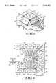
- FIG. 1Shown in FIG. 1 is an illustration of one embodiment of the thin, molded electronic device 10 surface mounted to a printed circuit board (PCB) 12 having a plurality of traces 14 terminating in bonding lands 16.
- PCBprinted circuit board
- FIG. 1Shown in FIG. 1 is an illustration of one embodiment of the thin, molded electronic device 10 surface mounted to a printed circuit board (PCB) 12 having a plurality of traces 14 terminating in bonding lands 16.
- PCBprinted circuit board
- the term PCBis used throughout the specification and claims herein, that the term is meant to include equivalents thereof, including but not necessarily limited to flex circuits.
- the substrate 32may be identical in materials and even in size to the PCB upon which it will be mounted.
- Device 10has a body 18, which in turn may comprise a base 20 that may be plastic molded over the electronic component (not shown in this Figure) and a cap 22. Extending from the package body 18 are a plurality of lead arrays 24 possessing a plurality of electrically conductive runners or traces terminating in outer bonding areas (not shown in this Figure) which are physically and electrically bonded to the bonding lands 16.
- the particular device 10 shown in FIG. 1has a square shape with four sides, each having a lead array 24, and thus, they may be termed lead "quad" arrays since they number four. It will be appreciated, however, that device 10 may in some embodiments have more or less than four arrays 24.
- Each arraymay be provided with an alignment mechanism at some point thereon, which in the design illustrated in FIG. 1 are tabs 26 on each side of the array 24, where the tabs 26 have holes 28 designed to correspond and mate with posts 30 in the PCB 12 to properly position the leads with the bonding lands 16.
- Device 10may also bear a heat spreader or heat sink 31 on its upper surface to help channel thermal energy from inside the package 10 to the outside.
- Lead arrays 24may be transparent or translucent as seen in array 24', and traces 34 may be visible therethrough. This option has the advantage of permitting visual inspection of the bonds made between traces 34 and lands 16.
- FIG. 2Shown in FIG. 2 is a layout of a thin, flexible substrate 32 which will form the backing for the lead arrays 24 as will be explained.
- Two embodiments of the thin, flexible substrate 32 and 32'are depicted in FIG. 2, separated by a dashed line 33, as Version A and Version B, respectively. It will be understood that on an actual substrate, the entire substrate would be either the design seen in Version A, or that seen in Version B. However, in this way the differences and similarities between the two versions can be better appreciated.
- Thin, flexible substrate 32/32'may be made from any very thin insulative material, such as those typically suitable for a tape automated bonding (TAB) backing layer or substrate.
- TABtape automated bonding
- Polyimideis a representative material, but is certainly not the only one; it may be found under trade names such as Uplex or Kapton, among others.
- Other suitable materialsinclude, but are not necessarily limited to polyester (lower in cost and performance than polyimide), Mylar and composites, such as a resin-filed epoxy or a fiber reinforced materials.
- the substrateshould be a material that can bear a plurality of conductive traces 34/34' thereon which may be formed by any suitable method, including conventional ones not limited to plating, etching, photolithography, printing, etc.
- the materialshould also be flexible enough to be formed into the lead arrays 24 at a point late in the fabrication process as will be explained later.
- the adhesion of the substrate 32/32' to the traces 34/34'should also be great enough that the traces 34/34' will not delaminate or separate from the substrate 32/32' when the lead arrays 24 are formed.
- substrate 32has an electronic component receiving area 36, which happens to be centrally located on the substrate 32 although it could be positioned elsewhere. While it will be appreciated that a wide variety of electronic components may be contained within the device 10 of the present invention, the invention may find one of its best uses as a package for integrated circuits. Thus, FIG. 2 shows an integrated circuit die 38 bearing a plurality of bonding pads 40 on its periphery, already die bonded to the integrated circuit die receiving area 36. It will also be appreciated that more than one chip 38 may be secured to the die receiving area and interconnected to the traces.
- traces 34Configured around the die receiving area 36 are a plurality of traces 34 which form a "lead frame" around the die 38, although it will be appreciated that these traces 34 are considerably thinner than what are conventionally thought of as leads in a lead frame. Traces 34 have inner bonding areas 42 arranged near or on die receiving area 36. At the outer periphery 44 of substrate 32 are a plurality of test points 46, one for each trace 34. Peripheries 44, which on a square substrate 32 number four are joined together at their ends by corners 48 such that a carrier structure or "ring" surrounds the die 38.
- traces 34are perpendicular to the edge of die receiving area 36 and parallel to each other until they reach the outer bonding areas 50 at which point they fan out or radiate to test points 46.
- Version Bdiffers. Traces 34' of Version B immediately begin fanning out or radiating from inner bonding pads 42 to outer bonding areas 50' and continue radiating out to test points 46. In other words, although the end points of traces 34 and 34' are the same, the paths they take through differently positioned outer bonding areas 50 and 50', respectively, are different.
- outer bonding areas 50may be at different pitches for different applications and the test points 46 remain at a the same or "standard" pitch for the test devices. It is anticipated that a plurality of outer bonding pads 50 may be arranged along traces 34, and that the end user may crop the periphery at a desired point to provide a device with leads at the correct pitch. This feature permits one package to be made for a variety of applications.
- slots 52 and 52'Separating the main quadrants of substrate 32 are slots 52 and 52' for Versions A and B, respectively.
- the shape of slots 52 and 52'depend on the shape of traces 34 and 34'. Because traces 34 are parallel and do not fan out between inner bonding areas 42 and outer bonding areas 50 as depicted in Version A of FIG. 2, slot 52 have sides 54 at a right angle to each other.
- Slots 52may be shaped to permit the presence of an alignment mechanism, which may be, but is not limited to, tabs 26 bearing holes 28. Because slots 52' are differently shaped, tabs 26' would have a triangular shape and alignment holes 28' would be spaced somewhat wider apart.
- slots 52may be considered optional, though they may be preferred in some applications.
- a device 10is anticipated where slots 52 are not present, but the portions of the substrate that might occupy the space where slots 52 might be are simply folded or telescoped inward to permit the lead arrays 24 to be formed or "downwardly" extended to permit the outer bonding areas 50 to contact the PCB bonding lands 16.
- FIG. 3Shown in FIG. 3 is a cross-sectional profile of a thin electronic device 10 of this invention under construction. Similar parts will have the same reference numbers, and the construction of the device 10 will be described.
- Substrate 32is provided and bears a plurality of traces 34 seen edge-on having inner bonding areas 42, outer bonding areas 50 and test points 46 at the terminals of traces 34.
- Integrated circuit die 38is next placed on the integrated circuit die receiving area 36 and die bonded thereto by a suitable adhesive 58.
- Bonding pads 40(not visible in this view) are next electrically connected to inner bonding areas 42 by any suitable means, including, but not limited to, wire bonds 60, tape automated bonding (TAB), "flip chip” bump bonding, etc.
- TABtape automated bonding
- die bonding pads 40would be provided with bumps of gold or other suitable material, inner bonding areas 42 would extend into the die receiving area 36 and the die 38 would be flipped over and directly bonded by thermocompression or other suitable technique to the inner bonding areas directly, which may also be bumped prior to bonding.
- the device 10may then be provided with a package body 18, which, in the embodiment seen in FIGS. 3 and 4, comprises an overmolded base 20.
- Base 20covers at least the integrated circuit die 38, the inner bonding areas 42 and wire bonds 60.
- the device 10is oriented on its top or upside-down from the position in which it will be mounted to a PCB 12, so although the "base" 20 is depicted on the top in FIG. 3, it will eventually form the bottom of the device 10 in FIG. 4.
- Body 18may be provided in other ways besides over-molding, such as enclosing the device with pre-formed piece parts, etc.
- the devicemay now be tested by contacting test probes with test points 46. Testing may occur prior to providing the body 48 as well. Being able to test the integrated circuit die 38 and its connections 60 to traces 34 before the device 10 is completely formed has the advantage of being able to discard or rework defective device 10 and chip 38 before additional value is added to the device 10 by subsequent steps.
- the substrate 32 peripheries 44 and corners 48 which form the surrounding carrier structureare severed along crop line 56.
- the slots 52which are not visible in FIGS. 3 and 4, may be formed at many places in the device 10 fabrication process including, but not necessarily limited to, before the die 38 is mounted to the substrate 32, after the overmolding step, and during or after the cropping along line 56. However, slots 52, if needed, must be present prior to the forming of at least the parts of substrate 32 and traces 34 (including outer bonding areas 50) into lead arrays 24 by bending and shaping. It is apparent that the resulting lead arrays 24 are separated by the slots 52 and that arrays 24 extend outside of and away from package body 18.
- traces 34 outside body 18 and including outer bonding areas 50may be formed into any suitable shape, such as the gull-wing configuration seen in FIG. 4, that will enable the outer bonding areas 50 to meet with and be bonded to the bonding lands 16 on PCB 12.
- Other configurationsinclude, but are not necessarily limited to butt joint and J-lead configurations. If lead arrays 24 are formed into a gull wing configuration, the package 10 must be inverted from the orientation of FIG. 3 which is probably more convenient for manufacture, to that position seen in FIG. 4.
- An alternate embodimentwould be to have the thin, flexible substrate 32 bear conductive traces 34 on both sides, which sets of traces are in electrical contact with each other. With such a substrate, the die 38 could be mounted on either side and either side of the arrays 24 could be used for bonding to the larger PCB substrate. With such a substrate 32, device 10 can be mounted to PCB substrate 12 in the position illustrated in FIG. 3.
- the actual bonding of the outer bonding areas 50 to the bonding lands 16may be conducted by any suitable manner, including but not necessarily limited to, tinning the two surfaces with solder, thermocompression bonding, wave solder, hot bar reflow, etc.
- Device 10may be optionally provided with a structure on the back side thereof or top in the orientation of FIG. 4, which may be a cap 22 that may be necessary in some instances to seal the package 10.
- Cap 22may contain a heat dissipation surface 62, or may in its entirety be a heat sink. In a preferred embodiment, the cap 22 is placed or formed at the same time as the base 20. However, if a separate heat sink is to be provided, it may be desirable to place the heat sink on the package 10 at least after the device 10 is tested to avoid unnecessarily affixing heat sinks to defective packages.
- the lead arrays 24will provide considerable flexibility and stress relief as the device 10 is handled, mounted on PCB 12, and while it is on the board 12 itself. Additionally, the substrate 32 and the PCB 12 can be better matched for thermal expansion properties to also reduce the stress. Further, because the traces 34 and outer bonding areas 50 are ganged together on a lead array 24, only one alignment need be made per device 10 side to ensure the alignment of all of the connections. The device 10 may also be tested at a larger pitch at test points 46 than the pitch available at lead areas 50. Bent lead and coplanarity problems are greatly reduced by the use of lead arrays 24. The device 10 can be made very thinly and can be readily surface mounted.
- test points 46, peripheries 44 and corners 48form a structure around the substrate 12 that will protect it during handling and testing. Damage that may occur to these regions during handling and testing is insignificant since this portion will be excised and discarded after testing and prior to mounting to the PCB 12.
- FIG. 5Shown in FIG. 5 is an embodiment of the invention where the IC die receiving area 36 is replaced by a thermally conductive die support 64 to which the die 38 is bonded.
- a heat spreader or heat sink 66may be provided and attached to thermally conductive die support 64.
- FIGS. 6 and 7show alternate body 18 configurations to those discussed before.
- resin dams 68are provided, which may be a suitable insulative, protective material.
- Resin dams 68may be molded in place on the substrate 32, or may be premolded and placed in a separate step.
- Resin 70is then provided to fill the space between dams 68.
- Resin 70is preferably an insulative material that is viscous upon placement, but which hardens over time or the application of heat. Suitable resins include, but are not limited to epoxies.
- the body 18may be finished by just applying the resin in bulk form 70' without using dams 68, as seen in FIG. 7. Such an application of resin is sometimes called "glob top".
- TAB interconnectionis not explicitly shown, it may certainly be used.
- substrate 32may be made from a transparent material permitting inspection of the bonds made on bonding lands 16. If substrate 32 were transparent, point-to-point localized laser fusing techniques could be used to make each of the connections. It is intended that all such modifications be included within the invention as fall within the scope of the appended claims.
Landscapes
- Engineering & Computer Science (AREA)
- Microelectronics & Electronic Packaging (AREA)
- Computer Hardware Design (AREA)
- Power Engineering (AREA)
- Physics & Mathematics (AREA)
- Condensed Matter Physics & Semiconductors (AREA)
- General Physics & Mathematics (AREA)
- Manufacturing & Machinery (AREA)
- Lead Frames For Integrated Circuits (AREA)
Abstract
Description
Claims (6)
Priority Applications (1)
| Application Number | Priority Date | Filing Date | Title |
|---|---|---|---|
| US07/567,838US5053357A (en) | 1989-12-27 | 1990-08-14 | Method of aligning and mounting an electronic device on a printed circuit board using a flexible substrate having fixed lead arrays thereon |
Applications Claiming Priority (2)
| Application Number | Priority Date | Filing Date | Title |
|---|---|---|---|
| US07/457,648US5018005A (en) | 1989-12-27 | 1989-12-27 | Thin, molded, surface mount electronic device |
| US07/567,838US5053357A (en) | 1989-12-27 | 1990-08-14 | Method of aligning and mounting an electronic device on a printed circuit board using a flexible substrate having fixed lead arrays thereon |
Related Parent Applications (1)
| Application Number | Title | Priority Date | Filing Date |
|---|---|---|---|
| US07/457,648DivisionUS5018005A (en) | 1989-12-27 | 1989-12-27 | Thin, molded, surface mount electronic device |
Publications (1)
| Publication Number | Publication Date |
|---|---|
| US5053357Atrue US5053357A (en) | 1991-10-01 |
Family
ID=27038688
Family Applications (1)
| Application Number | Title | Priority Date | Filing Date |
|---|---|---|---|
| US07/567,838Expired - LifetimeUS5053357A (en) | 1989-12-27 | 1990-08-14 | Method of aligning and mounting an electronic device on a printed circuit board using a flexible substrate having fixed lead arrays thereon |
Country Status (1)
| Country | Link |
|---|---|
| US (1) | US5053357A (en) |
Cited By (36)
| Publication number | Priority date | Publication date | Assignee | Title |
|---|---|---|---|---|
| US5249245A (en)* | 1992-08-31 | 1993-09-28 | Motorola, Inc. | Optoelectroinc mount including flexible substrate and method for making same |
| US5249101A (en)* | 1992-07-06 | 1993-09-28 | International Business Machines Corporation | Chip carrier with protective coating for circuitized surface |
| US5310702A (en)* | 1992-03-20 | 1994-05-10 | Kulicke And Soffa Industries, Inc. | Method of preventing short-circuiting of bonding wires |
| US5362680A (en)* | 1992-08-18 | 1994-11-08 | Texas Instruments Incorporated | Technique for enhancing adhesion capability of heat spreaders in molded packages |
| US5498575A (en)* | 1993-06-23 | 1996-03-12 | Matsushita Electric Industrial Co., Ltd. | Bonding film member and mounting method of electronic component |
| US5631191A (en)* | 1993-08-27 | 1997-05-20 | Poly-Flex Circuits, Inc. | Method for connecting a die to electrically conductive traces on a flexible lead-frame |
| US5646068A (en)* | 1995-02-03 | 1997-07-08 | Texas Instruments Incorporated | Solder bump transfer for microelectronics packaging and assembly |
| US5937277A (en)* | 1994-01-31 | 1999-08-10 | Fujitsu Limited | Semiconductor device with reliable electrodes of projecting shape and method of forming same |
| US6153503A (en)* | 1997-03-10 | 2000-11-28 | National Science Council | Continuous process for producing solder bumps on electrodes of semiconductor chips |
| US20010003049A1 (en)* | 1996-07-12 | 2001-06-07 | Norio Fukasawa | Method and mold for manufacturing semiconductor device, semiconductor device, and method for mounting the device |
| US6405429B1 (en)* | 1999-08-26 | 2002-06-18 | Honeywell Inc. | Microbeam assembly and associated method for integrated circuit interconnection to substrates |
| US6881611B1 (en) | 1996-07-12 | 2005-04-19 | Fujitsu Limited | Method and mold for manufacturing semiconductor device, semiconductor device and method for mounting the device |
| US20060076159A1 (en)* | 2004-10-12 | 2006-04-13 | International Business Machines Corporation | Contour structures to highlight inspection regions |
| US7297562B1 (en) | 2002-05-01 | 2007-11-20 | Amkor Technology, Inc. | Circuit-on-foil process for manufacturing a laminated semiconductor package substrate having embedded conductive patterns |
| US7365006B1 (en) | 2004-05-05 | 2008-04-29 | Amkor Technology, Inc. | Semiconductor package and substrate having multi-level vias fabrication method |
| US7399661B2 (en)* | 2002-05-01 | 2008-07-15 | Amkor Technology, Inc. | Method for making an integrated circuit substrate having embedded back-side access conductors and vias |
| US20080185696A1 (en)* | 2007-02-05 | 2008-08-07 | Ruben Madrid | Semiconductor die package including leadframe with die attach pad with folded edge |
| WO2009074264A3 (en)* | 2007-12-11 | 2009-09-03 | Saint-Gobain Glass France | Solder connection element |
| US7589398B1 (en) | 2006-10-04 | 2009-09-15 | Amkor Technology, Inc. | Embedded metal features structure |
| US7670962B2 (en) | 2002-05-01 | 2010-03-02 | Amkor Technology, Inc. | Substrate having stiffener fabrication method |
| US20100157557A1 (en)* | 2008-12-18 | 2010-06-24 | Yin-Hsiang Teng | Conductive wire pattern and method of monitoring the bonding error of a film |
| US7752752B1 (en) | 2007-01-09 | 2010-07-13 | Amkor Technology, Inc. | Method of fabricating an embedded circuit pattern |
| US20100294566A1 (en)* | 2007-12-11 | 2010-11-25 | Bernhard Reul | Windowpane having an electrical flat connecting element |
| US20110170261A1 (en)* | 2008-10-01 | 2011-07-14 | Sharp Kabushiki Kaisha | Electronic apparatus, illuminating device, display device and television receiver |
| US20110271522A1 (en)* | 2008-07-17 | 2011-11-10 | Charles Still | Method for making an electronic assembly |
| USRE43404E1 (en) | 1996-03-07 | 2012-05-22 | Tessera, Inc. | Methods for providing void-free layer for semiconductor assemblies |
| US8485840B2 (en) | 2007-09-20 | 2013-07-16 | Saint-Gobain Glass France | Electrical connecting element and disk equipped with such an element |
| US8826531B1 (en) | 2005-04-05 | 2014-09-09 | Amkor Technology, Inc. | Method for making an integrated circuit substrate having laminated laser-embedded circuit layers |
| US8872329B1 (en) | 2009-01-09 | 2014-10-28 | Amkor Technology, Inc. | Extended landing pad substrate package structure and method |
| US20150305191A1 (en)* | 2014-04-18 | 2015-10-22 | Raytheon Company | Method to align surface mount packages for thermal enhancement |
| CN105655265A (en)* | 2014-10-31 | 2016-06-08 | 矽品精密工业股份有限公司 | Non-sticking detection test method and substrate used therefor |
| US9812386B1 (en) | 2002-05-01 | 2017-11-07 | Amkor Technology, Inc. | Encapsulated semiconductor package |
| CN107431055A (en)* | 2015-11-20 | 2017-12-01 | 新电元工业株式会社 | Semiconductor device |
| US10811277B2 (en) | 2004-03-23 | 2020-10-20 | Amkor Technology, Inc. | Encapsulated semiconductor package |
| US11081370B2 (en) | 2004-03-23 | 2021-08-03 | Amkor Technology Singapore Holding Pte. Ltd. | Methods of manufacturing an encapsulated semiconductor device |
| US11094560B1 (en) | 2004-03-23 | 2021-08-17 | Amkor Technology Singapore Holding Pte. Ltd. | Encapsulated semiconductor package |
Citations (9)
| Publication number | Priority date | Publication date | Assignee | Title |
|---|---|---|---|---|
| US3718969A (en)* | 1970-09-21 | 1973-03-06 | Motorola Inc | Plastic encapsulated semiconductor assemblies |
| US3911568A (en)* | 1974-11-18 | 1975-10-14 | Gen Motors Corp | Method and apparatus for bonding miniature semiconductor pill-type components to a circuit board |
| US4411719A (en)* | 1980-02-07 | 1983-10-25 | Westinghouse Electric Corp. | Apparatus and method for tape bonding and testing of integrated circuit chips |
| JPS6365635A (en)* | 1986-09-05 | 1988-03-24 | Nec Corp | Integrated circuit mounted with film carrier tape |
| US4742431A (en)* | 1983-08-31 | 1988-05-03 | Kabushiki Kaisha Toshiba | Flexible circuit board |
| US4744009A (en)* | 1986-10-31 | 1988-05-10 | Amp Incorporated | Protective carrier and securing means therefor |
| US4766670A (en)* | 1987-02-02 | 1988-08-30 | International Business Machines Corporation | Full panel electronic packaging structure and method of making same |
| US4783719A (en)* | 1987-01-20 | 1988-11-08 | Hughes Aircraft Company | Test connector for electrical devices |
| US4792532A (en)* | 1985-12-25 | 1988-12-20 | Hitachi, Ltd. | Semiconductor device and process for producing the same, and tape carrier used in said process |
- 1990
- 1990-08-14USUS07/567,838patent/US5053357A/ennot_activeExpired - Lifetime
Patent Citations (9)
| Publication number | Priority date | Publication date | Assignee | Title |
|---|---|---|---|---|
| US3718969A (en)* | 1970-09-21 | 1973-03-06 | Motorola Inc | Plastic encapsulated semiconductor assemblies |
| US3911568A (en)* | 1974-11-18 | 1975-10-14 | Gen Motors Corp | Method and apparatus for bonding miniature semiconductor pill-type components to a circuit board |
| US4411719A (en)* | 1980-02-07 | 1983-10-25 | Westinghouse Electric Corp. | Apparatus and method for tape bonding and testing of integrated circuit chips |
| US4742431A (en)* | 1983-08-31 | 1988-05-03 | Kabushiki Kaisha Toshiba | Flexible circuit board |
| US4792532A (en)* | 1985-12-25 | 1988-12-20 | Hitachi, Ltd. | Semiconductor device and process for producing the same, and tape carrier used in said process |
| JPS6365635A (en)* | 1986-09-05 | 1988-03-24 | Nec Corp | Integrated circuit mounted with film carrier tape |
| US4744009A (en)* | 1986-10-31 | 1988-05-10 | Amp Incorporated | Protective carrier and securing means therefor |
| US4783719A (en)* | 1987-01-20 | 1988-11-08 | Hughes Aircraft Company | Test connector for electrical devices |
| US4766670A (en)* | 1987-02-02 | 1988-08-30 | International Business Machines Corporation | Full panel electronic packaging structure and method of making same |
Cited By (57)
| Publication number | Priority date | Publication date | Assignee | Title |
|---|---|---|---|---|
| US5310702A (en)* | 1992-03-20 | 1994-05-10 | Kulicke And Soffa Industries, Inc. | Method of preventing short-circuiting of bonding wires |
| US5249101A (en)* | 1992-07-06 | 1993-09-28 | International Business Machines Corporation | Chip carrier with protective coating for circuitized surface |
| US5362680A (en)* | 1992-08-18 | 1994-11-08 | Texas Instruments Incorporated | Technique for enhancing adhesion capability of heat spreaders in molded packages |
| US5422788A (en)* | 1992-08-18 | 1995-06-06 | Texas Instruments Incorporated | Technique for enhancing adhesion capability of heat spreaders in molded packages |
| US5249245A (en)* | 1992-08-31 | 1993-09-28 | Motorola, Inc. | Optoelectroinc mount including flexible substrate and method for making same |
| US5498575A (en)* | 1993-06-23 | 1996-03-12 | Matsushita Electric Industrial Co., Ltd. | Bonding film member and mounting method of electronic component |
| US5631191A (en)* | 1993-08-27 | 1997-05-20 | Poly-Flex Circuits, Inc. | Method for connecting a die to electrically conductive traces on a flexible lead-frame |
| US5937277A (en)* | 1994-01-31 | 1999-08-10 | Fujitsu Limited | Semiconductor device with reliable electrodes of projecting shape and method of forming same |
| US5646068A (en)* | 1995-02-03 | 1997-07-08 | Texas Instruments Incorporated | Solder bump transfer for microelectronics packaging and assembly |
| USRE43404E1 (en) | 1996-03-07 | 2012-05-22 | Tessera, Inc. | Methods for providing void-free layer for semiconductor assemblies |
| US20010003049A1 (en)* | 1996-07-12 | 2001-06-07 | Norio Fukasawa | Method and mold for manufacturing semiconductor device, semiconductor device, and method for mounting the device |
| US6881611B1 (en) | 1996-07-12 | 2005-04-19 | Fujitsu Limited | Method and mold for manufacturing semiconductor device, semiconductor device and method for mounting the device |
| US6153503A (en)* | 1997-03-10 | 2000-11-28 | National Science Council | Continuous process for producing solder bumps on electrodes of semiconductor chips |
| US6405429B1 (en)* | 1999-08-26 | 2002-06-18 | Honeywell Inc. | Microbeam assembly and associated method for integrated circuit interconnection to substrates |
| US20050048696A1 (en)* | 1999-08-26 | 2005-03-03 | Honeywell, Inc. | Microbeam assembly and associated method for integrated circuit interconnection to substrates |
| US7670962B2 (en) | 2002-05-01 | 2010-03-02 | Amkor Technology, Inc. | Substrate having stiffener fabrication method |
| US8322030B1 (en)* | 2002-05-01 | 2012-12-04 | Amkor Technology, Inc. | Circuit-on-foil process for manufacturing a laminated semiconductor package substrate having embedded conductive patterns |
| US7399661B2 (en)* | 2002-05-01 | 2008-07-15 | Amkor Technology, Inc. | Method for making an integrated circuit substrate having embedded back-side access conductors and vias |
| US9812386B1 (en) | 2002-05-01 | 2017-11-07 | Amkor Technology, Inc. | Encapsulated semiconductor package |
| US10461006B1 (en) | 2002-05-01 | 2019-10-29 | Amkor Technology, Inc. | Encapsulated semiconductor package |
| US8316536B1 (en) | 2002-05-01 | 2012-11-27 | Amkor Technology, Inc. | Multi-level circuit substrate fabrication method |
| US7297562B1 (en) | 2002-05-01 | 2007-11-20 | Amkor Technology, Inc. | Circuit-on-foil process for manufacturing a laminated semiconductor package substrate having embedded conductive patterns |
| US10811277B2 (en) | 2004-03-23 | 2020-10-20 | Amkor Technology, Inc. | Encapsulated semiconductor package |
| US11081370B2 (en) | 2004-03-23 | 2021-08-03 | Amkor Technology Singapore Holding Pte. Ltd. | Methods of manufacturing an encapsulated semiconductor device |
| US11094560B1 (en) | 2004-03-23 | 2021-08-17 | Amkor Technology Singapore Holding Pte. Ltd. | Encapsulated semiconductor package |
| US7365006B1 (en) | 2004-05-05 | 2008-04-29 | Amkor Technology, Inc. | Semiconductor package and substrate having multi-level vias fabrication method |
| US20080244904A1 (en)* | 2004-10-12 | 2008-10-09 | International Business Machines Corporation | Contour Structures to Highlight Inspection Regions |
| US20060076159A1 (en)* | 2004-10-12 | 2006-04-13 | International Business Machines Corporation | Contour structures to highlight inspection regions |
| US7614147B2 (en) | 2004-10-12 | 2009-11-10 | International Business Machines Corporation | Method of creating contour structures to highlight inspection region |
| US7411135B2 (en) | 2004-10-12 | 2008-08-12 | International Business Machines Corporation | Contour structures to highlight inspection regions |
| US8826531B1 (en) | 2005-04-05 | 2014-09-09 | Amkor Technology, Inc. | Method for making an integrated circuit substrate having laminated laser-embedded circuit layers |
| US11848214B2 (en) | 2006-08-01 | 2023-12-19 | Amkor Technology Singapore Holding Pte. Ltd. | Encapsulated semiconductor package |
| US7589398B1 (en) | 2006-10-04 | 2009-09-15 | Amkor Technology, Inc. | Embedded metal features structure |
| US7911037B1 (en) | 2006-10-04 | 2011-03-22 | Amkor Technology, Inc. | Method and structure for creating embedded metal features |
| US7752752B1 (en) | 2007-01-09 | 2010-07-13 | Amkor Technology, Inc. | Method of fabricating an embedded circuit pattern |
| US20080185696A1 (en)* | 2007-02-05 | 2008-08-07 | Ruben Madrid | Semiconductor die package including leadframe with die attach pad with folded edge |
| US20110008935A1 (en)* | 2007-02-05 | 2011-01-13 | Fairchild Semiconductor Corporation | Semiconductor die package including leadframe with die attach pad with folded edge |
| US7821116B2 (en) | 2007-02-05 | 2010-10-26 | Fairchild Semiconductor Corporation | Semiconductor die package including leadframe with die attach pad with folded edge |
| US8485840B2 (en) | 2007-09-20 | 2013-07-16 | Saint-Gobain Glass France | Electrical connecting element and disk equipped with such an element |
| US20100294566A1 (en)* | 2007-12-11 | 2010-11-25 | Bernhard Reul | Windowpane having an electrical flat connecting element |
| US9155206B2 (en) | 2007-12-11 | 2015-10-06 | Saint-Gobain Glass France | Solder connection element |
| WO2009074264A3 (en)* | 2007-12-11 | 2009-09-03 | Saint-Gobain Glass France | Solder connection element |
| US20100319977A1 (en)* | 2007-12-11 | 2010-12-23 | Mitja Rateiczak | Solder connection element |
| US8481857B2 (en) | 2007-12-11 | 2013-07-09 | Saint-Gobain Glass France | Windowpane having an electrical flat connecting element |
| US20110271522A1 (en)* | 2008-07-17 | 2011-11-10 | Charles Still | Method for making an electronic assembly |
| US8333011B2 (en)* | 2008-07-17 | 2012-12-18 | Autoliv Asp, Inc. | Method for making an electronic assembly |
| US20110170261A1 (en)* | 2008-10-01 | 2011-07-14 | Sharp Kabushiki Kaisha | Electronic apparatus, illuminating device, display device and television receiver |
| US8144472B2 (en)* | 2008-12-18 | 2012-03-27 | Chunghwa Picture Tubes, Ltd. | Conductive wire pattern and method of monitoring the bonding error of a film |
| US20100157557A1 (en)* | 2008-12-18 | 2010-06-24 | Yin-Hsiang Teng | Conductive wire pattern and method of monitoring the bonding error of a film |
| TWI402566B (en)* | 2008-12-18 | 2013-07-21 | Chunghwa Picture Tubes Ltd | Pad region having conductive wire pattern and method of monitoring the bonding error of a film |
| US9462704B1 (en) | 2009-01-09 | 2016-10-04 | Amkor Technology, Inc. | Extended landing pad substrate package structure and method |
| US8872329B1 (en) | 2009-01-09 | 2014-10-28 | Amkor Technology, Inc. | Extended landing pad substrate package structure and method |
| US20150305191A1 (en)* | 2014-04-18 | 2015-10-22 | Raytheon Company | Method to align surface mount packages for thermal enhancement |
| US9554488B2 (en)* | 2014-04-18 | 2017-01-24 | Raytheon Company | Method to align surface mount packages for thermal enhancement |
| CN105655265A (en)* | 2014-10-31 | 2016-06-08 | 矽品精密工业股份有限公司 | Non-sticking detection test method and substrate used therefor |
| CN107431055A (en)* | 2015-11-20 | 2017-12-01 | 新电元工业株式会社 | Semiconductor device |
| CN107431055B (en)* | 2015-11-20 | 2019-07-26 | 新电元工业株式会社 | Semiconductor device |
Similar Documents
| Publication | Publication Date | Title |
|---|---|---|
| US5018005A (en) | Thin, molded, surface mount electronic device | |
| US5053357A (en) | Method of aligning and mounting an electronic device on a printed circuit board using a flexible substrate having fixed lead arrays thereon | |
| US5045921A (en) | Pad array carrier IC device using flexible tape | |
| US8008129B2 (en) | Method of making semiconductor device packaged by sealing resin member | |
| KR0169820B1 (en) | Chip scale package with metal wiring substrate | |
| US5239198A (en) | Overmolded semiconductor device having solder ball and edge lead connective structure | |
| US7851906B2 (en) | Flexible circuit electronic package with standoffs | |
| US5557150A (en) | Overmolded semiconductor package | |
| US5045914A (en) | Plastic pad array electronic AC device | |
| JP3588801B2 (en) | Method for manufacturing semiconductor device | |
| US6174751B1 (en) | Method of manufacturing resin encapsulated semiconductor device | |
| KR970011619B1 (en) | Leadless pad array chip carrier package and manufacturing method thereof | |
| EP0623954B1 (en) | Molded plastic packaging of electronic devices | |
| TW200534454A (en) | Exposed pad module integrated a passive device therein | |
| KR100614431B1 (en) | Structure and method for manufacturing semiconductor package device of improved yield | |
| JP3366062B2 (en) | Overmold type semiconductor device and method of manufacturing the same | |
| KR19980068343A (en) | Chip scale semiconductor package using flexible circuit board and manufacturing method thereof | |
| US20070164404A1 (en) | Semiconductor package | |
| JPS63174344A (en) | Pin grid array | |
| KR100911461B1 (en) | Semiconductor package | |
| JP2538937B2 (en) | Semiconductor package | |
| JPS63226043A (en) | Semiconductor device | |
| JP2004179300A (en) | Semiconductor device and its manufacturing method | |
| JPH1117067A (en) | Semiconductor device and manufacturing method thereof | |
| KR19990056765A (en) | Chip size package |
Legal Events
| Date | Code | Title | Description |
|---|---|---|---|
| STCF | Information on status: patent grant | Free format text:PATENTED CASE | |
| FEPP | Fee payment procedure | Free format text:PAYOR NUMBER ASSIGNED (ORIGINAL EVENT CODE: ASPN); ENTITY STATUS OF PATENT OWNER: LARGE ENTITY | |
| FPAY | Fee payment | Year of fee payment:4 | |
| REMI | Maintenance fee reminder mailed | ||
| FPAY | Fee payment | Year of fee payment:8 | |
| SULP | Surcharge for late payment | ||
| FPAY | Fee payment | Year of fee payment:12 | |
| AS | Assignment | Owner name:FREESCALE SEMICONDUCTOR, INC., TEXAS Free format text:ASSIGNMENT OF ASSIGNORS INTEREST;ASSIGNOR:MOTOROLA, INC.;REEL/FRAME:015698/0657 Effective date:20040404 Owner name:FREESCALE SEMICONDUCTOR, INC.,TEXAS Free format text:ASSIGNMENT OF ASSIGNORS INTEREST;ASSIGNOR:MOTOROLA, INC.;REEL/FRAME:015698/0657 Effective date:20040404 | |
| AS | Assignment | Owner name:CITIBANK, N.A. AS COLLATERAL AGENT, NEW YORK Free format text:SECURITY AGREEMENT;ASSIGNORS:FREESCALE SEMICONDUCTOR, INC.;FREESCALE ACQUISITION CORPORATION;FREESCALE ACQUISITION HOLDINGS CORP.;AND OTHERS;REEL/FRAME:018855/0129 Effective date:20061201 Owner name:CITIBANK, N.A. AS COLLATERAL AGENT,NEW YORK Free format text:SECURITY AGREEMENT;ASSIGNORS:FREESCALE SEMICONDUCTOR, INC.;FREESCALE ACQUISITION CORPORATION;FREESCALE ACQUISITION HOLDINGS CORP.;AND OTHERS;REEL/FRAME:018855/0129 Effective date:20061201 | |
| AS | Assignment | Owner name:FREESCALE SEMICONDUCTOR, INC., TEXAS Free format text:PATENT RELEASE;ASSIGNOR:CITIBANK, N.A., AS COLLATERAL AGENT;REEL/FRAME:037354/0225 Effective date:20151207 |