US5050165A - Bridge circuit for interconnecting networks - Google Patents
Bridge circuit for interconnecting networksDownload PDFInfo
- Publication number
- US5050165A US5050165AUS07/359,568US35956889AUS5050165AUS 5050165 AUS5050165 AUS 5050165AUS 35956889 AUS35956889 AUS 35956889AUS 5050165 AUS5050165 AUS 5050165A
- Authority
- US
- United States
- Prior art keywords
- message
- signals
- circuit
- address
- signal
- Prior art date
- Legal status (The legal status is an assumption and is not a legal conclusion. Google has not performed a legal analysis and makes no representation as to the accuracy of the status listed.)
- Expired - Lifetime
Links
- 230000015654memoryEffects0.000abstractdescription95
- 238000012545processingMethods0.000abstractdescription9
- 125000004122cyclic groupChemical group0.000abstractdescription2
- 238000001514detection methodMethods0.000description13
- 230000003287optical effectEffects0.000description10
- 238000010586diagramMethods0.000description8
- 230000005540biological transmissionEffects0.000description7
- 238000000034methodMethods0.000description5
- 239000000835fiberSubstances0.000description3
- 230000008569processEffects0.000description3
- 230000002159abnormal effectEffects0.000description2
- 238000005070samplingMethods0.000description2
- 101100172132Mus musculus Eif3a geneProteins0.000description1
- 230000008901benefitEffects0.000description1
- 230000008859changeEffects0.000description1
- 230000006870functionEffects0.000description1
- 230000006872improvementEffects0.000description1
- 230000010387memory retrievalEffects0.000description1
- 239000013307optical fiberSubstances0.000description1
- 238000011112process operationMethods0.000description1
- 230000004044responseEffects0.000description1
Images


Classifications
- H—ELECTRICITY
- H04—ELECTRIC COMMUNICATION TECHNIQUE
- H04L—TRANSMISSION OF DIGITAL INFORMATION, e.g. TELEGRAPHIC COMMUNICATION
- H04L12/00—Data switching networks
- H04L12/28—Data switching networks characterised by path configuration, e.g. LAN [Local Area Networks] or WAN [Wide Area Networks]
- H04L12/46—Interconnection of networks
- H04L12/4604—LAN interconnection over a backbone network, e.g. Internet, Frame Relay
- H04L12/462—LAN interconnection over a bridge based backbone
- H04L12/4625—Single bridge functionality, e.g. connection of two networks over a single bridge
- H—ELECTRICITY
- H04—ELECTRIC COMMUNICATION TECHNIQUE
- H04L—TRANSMISSION OF DIGITAL INFORMATION, e.g. TELEGRAPHIC COMMUNICATION
- H04L45/00—Routing or path finding of packets in data switching networks
- H04L45/74—Address processing for routing
- H04L45/742—Route cache; Operation thereof
Definitions
- the present inventionrelates to a bridge circuit for interconnecting networks for storing information of the addresses of stations in a local area network which send and receive a message, effectively connecting two local area networks with each other.
- a conventional bridge circuit for interconnecting networks with each otheris the subject of U.S. Pat. No. 4,597,078 assigned to Digital Equipment Corporation.
- the bridge circuitis dealing with two local networks. There is connected to a first local network a first control device and to a second local network a second control device.
- the control devicesends an interrupt signal to a microprocessor. Meantime the message has been stored in a RAM.
- the microprocessoris aware of which network has sent the message and fetches the destination address of the message from the RAM to a look-up controller circuit.
- the look-up controller circuitis designed to take the destination address information and compares it against a group of destination addresses which are held in a look-up RAM.
- the destination address information, in the look-up RAMincludes a tag which indicates whether the destination address belongs to a station in the first or second local network. If there is a match between the destination address of the message and a destination address in the look-up RAM, the microprocessor will send the message to the proper station through the bridge, or ignore the message if the sending station is on the same local network as the receiving station. If there is no match, i.e., it represents a new station, the message will be sent to the other network. In the latter case when such a new station becomes a source station, its address will be recorded so that the next time such a station is a destination.
- the microprocessorstores the addresses of the sending and receiving stations in the memory, creates a table of the addresses of the stations corresponding to each network, retrieves the addresses in the table, and judges whether the message is to be sent to the other network or not.
- the transferring speed of a messageis restricted not by the physical speed of the networks but by the processing speed of the microprocessor in the bridge circuit.
- An object and advantage of the present inventionis to provide a novel bridge circuit for interconnecting networks which increases the transferring speed of a message between the networks.
- Another object of the present inventionis to provide a novel bridge circuit for interconnecting networks in which a microprocessor processes an operation of sending a receiving message from on network to the other network but does not process operations such as the storing of the address of the sending station and the receiving station, the retrieving of the address, and judging whether the receiving message is to be sent to the other network or not.
- a further object of the present inventionis to provide a novel bridge circuit for interconnecting networks in which a microprocessor judges whether a message receiving operation is continued or stopped in accordance with the address of the receiving station.
- the addressesare subject to CRC.
- the results of the CRC of the source addressare written into a memory by bits as the addresses information during the message receiving operation, whereby the sending stations in the network from which the message has been received by the bridge circuit are stored.
- the bits of the memoryare read while using the results of the CRC of the destination address, and from the content of the thus-read bits, whether or not the receiving station exists in the network from which the message has been received is retrieved and judged.
- the receiving stationis judged to exist in the network from which the message has been received by the bridge circuit, a signal for stopping the receiving operation of the message is generated, thereby cancelling the receiving operation. If the means having the above-described structure is provided on each receiving means of the two networks so as to constitute a bridge circuit, the microprocessor in the bridge circuit need not execute the conventional table retrieval and has only to send the message normally received from one network to the other network.
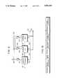
- FIG. 1is a basic block diagram of the system according to the present invention.
- FIG. 2is a block diagram showing the connection among an encoder-decoder, a synchronization circuit, a CRC computing circuit, decision circuit, and LAN controller shown in FIG. 1;
- FIG. 3shows the format of a message used in the system shown in FIG. 1;
- FIG. 4shows an format of the address of a station in the message shown in FIG. 3;
- FIG. 5shows the correspondence between the addresses obtained by the CRC computing circuit and data bits of a look-up memory
- FIG. 6 and 7are block diagrams of the memory control circuit controlling the look-up memory
- FIG. 8is a system block diagram in another embodiment of the present invention.
- FIG. 9is a block diagram of a Fiber Distributed Data Interface control circuit.
- FIG. 10shows the format of a message used in the Fiber Distributed Data Interface.
- FIG. 1shows an embodiment of the present invention in an Ethernet local area network.
- a first networkhas stations 1A and 2A which are connected to a segment 1 each through transceivers T1 and T2.
- a second networkhas stations 1B and 2B which are connected to a segment 2 each through transceivers T5 and T6.
- the first network and the second networkare connected with each other by a bridge circuit 3 comprising identical first and second circuit means through transceivers T3 and T4.
- the number of stations connected to each networkcould be more than two.
- the first networkis connected to an encoder-decoder 11 and the second network is connected to an encoder-decoder 13.
- the encoder-decoder 11is connected to a LAN controller 12 and a synchronization circuit 31 through a bus 15.
- the encoder-decoder 13is connected to a LAN controller 14 and a synchronization circuit 34 through a bus 18.
- a device i82501 produced by INTEL and a device Am7992B produced by ADVANCED MICRO DEVICE(hereinunder referred to as "AMD") is usable.
- ADVANCED MICRO DEVICEhereinunder referred to as "AMD"
- ADVANCED MICRO DEVICEhereinunder referred to as "AMD”
- ADVANCEDMICRO DEVICE
- a device i82586produced by INTEL, for example, is usable.
- the LAN controller 12is connected to a memory control circuit 62 through a bus 21.
- the memory control circuit 62is connected to a buffer memory 63 through a bus 65.
- the LAN controller 14is connected to the memory control circuit 62 through a bus 22 in such a manner as to be accessible to the buffer memory 63 through the bus 65.
- Predetermined messagesare transferred between each network by a microprocessor (hereinunder referred to as "MPU") 61 which controls the LAN controllers 12 and 14.
- MPUmicroprocessor
- the MPU 61supplies a channel attention signal for starting to the LAN controller 12 through a line 25 and when the LAN controller 12 has completed the reception of the message, the LAN controller 12 supplies an interrupt signal to the MPU 61 through a line 23. While the LAN controller 12 is receiving the message, the message is supplied to the buffer memory 63 through the memory control circuit 62.
- the MPU 61supplies a channel attention signal for starting to the LAN controller 14 through a line 26 and when the LAN controller 14 has completed the transmission of the message, the LAN controller 14 supplies an interrupt signal to the MPU 61 through a line 24. While the LAN controller 14 is sending the message to the second network, the LAN controller 14 receives the sending message from the buffer memory 63 the microprocessor 61, memory control circuit 62 and Lan controllers 12, 14 all comprising means for sending predetermined message signals to the respective local area networks.
- collision detection signalsare sensed by transceiver T3 or T4 during transferring a message.
- the LAN controller 12 or 14supplies an interrupt signal to the MPU 61 as a sending or receiving error, whereby the message sending or receiving operation is stopped.
- the synchronization circuit 31synchronizes with the source address and destination address in the message received from the encoder-decoder 11, and supplies the addresses to a computing means comprising a CRC computing circuit 32 or code generating means through a bus 37.
- the CRC computation circuit 32is connected to comparing means which comprises a memory control circuit 51 and a look-up memory 52 through a bus 38, and supplies a request for accessing to the look-up memory or addressable means for storing source addresses 52 while using the results of the cyclic redundancy check of the addresses as a memory address.
- the memory control circuit 51reads from and writes into the look-up memory 52 through a bus 55.
- the data or coded signals read from the look-up memory 52are supplied to a decision circuit 33 through a bus 56, and the decision circuit 33 outputs a stop signal or a decision signal on a line 39 as the result of decision that the destination address is located in the first network.
- a logical OR gate 4receives the stop signal through the line 39 and the collision detection signal through the line 17. The logical sum output from the OR gate 4 is input to the LAN controller 12 through a line 43. When the stop signal appears on the line 39 during sending a message, the LAN controller 12 supplies the interrupt signal to the MPU 61 because the destination address is located in the first network.
- a CRC computing circuit 35a memory control circuit 53 and a look-up memory 54 are connected to each other through buses 40, 41 and 57, respectively.
- the data read from the look-up memory 54is supplied to a decision circuit 36 through a bus 58.
- the logical sum of the stop signal on a line 42 output from the decision circuit 36 and the collision detection signal on a line 20is input to the LAN controller 14 through a line 44.
- the look-up memories 52 and 54 shown in FIG. 1are initialized by the MPU 61. A method of initialization will be explained later with reference to FIGS. 5 and 6.
- FIG. 3shows the format of a message used in the system shown in FIG. 1.
- the messagehas synchronization bits, a destination address, a source address, a data portion and frame check bits.
- FIG. 4shows the format of the address of a station in the message shown in FIG. 3.
- the addresshas a company code having 24 bits, and optional bits having 24 bits.
- a message sent from the station 1Ais sent to the segment 1 through a transceiver T1 and input to the encoder-decoder 11 through a transceiver T3.
- the encoder-decoder 11decodes the encoded message, separates it into a receiving clock 131 and receiving data 132, as shown in FIG. 2, and supplies the receiving clock 131 and receiving data 132 to the LAN controller 12.
- the encoder-decoder 11also supplies a carrier detection signal 16 and a collision detection signal 17 to the LAN controller 12.
- the LAN controller 12receives the receiving data 132 in synchronization with the receiving clock 131 when the carrier detection signal 16 becomes effective, and transfers the message to the buffer memory 63, as described above. If the collision detection signal 17 does not appear during receiving the message or when an error is not detected in the reception of the message, the LAN controller 12 supplies an interrupt signal to the MPU 61 through the line 23 so as to indicate that the reception is normal.
- the LAN controller 12supplies an interrupt signal to the MPU 61 so as to indicate that the reception is abnormal.
- the MPU 61supplies a channel attention signal to the LAN controller 14 through the line 26 and starts the LAN controller 14 so as to supply the message from the station 1A which has been memorized in the buffer memory 63 to the segment 2.
- the interrupt signalindicates the abnormal reception
- the MPU 61abandons the received message and does not supply it to the segment 2.
- the receiving clock 131, the receiving data 132 and the carrier detection signal 16 output from the encoder-decoder 11are input to the synchronization circuit 31 and the carrier detection signal 16 is also input to the decision circuit 33, as shown in FIG. 2.
- the synchronization circuit 31samples the receiving data in synchronization with the receiving clock 131, and when the synchronization bits shown in FIG. 3 are detected, the synchronization circuit 31 supplies an arithmetic data 137 which is comprised of a destination address, source address, data portion and frame check bits, a sampling clock 136 and an operation enabling signal 138 to a CRC computing circuit 31.
- the CRC computing circuit 32computes the CRC operation of the arithmetic data 137 with respect to a predetermined bit length in synchronization with the sampling clock 136.
- the physical station addressis 48 bits in accordance with the format IEEE802.3, as shown in FIGS. 3 and 4. Especially, to a product having this format, 3 bytes which is called a company code is allotted. It is therefore possible to reduce the overlapping degree by carrying out CRC for each region in a physical station address comprising company code, optional bit, and station address and by allotting different bits to the respective addresses.
- the CRC computing circuit 32computes the CRC operation of the destination address after the synchronization bits, and outputs a memory request signal to the memory control circuit 51 through the bus 38.
- the memory request signalhas each result of the CRC operation on each region of the destination address shown in FIG. 5.
- the data bit in the look-up memory 52is allotted in the same way as the memory request signal by the memory control Circuit 51.
- the memory control circuit 51reads the bits from the look-up memory 52 with respect to the respective memory request signals computed by the CRC computing circuit 32, and inputs the read data to the decision circuit 33.
- the decision circuit 33outputs the stop signal 39 if the all bits read from the look-up memory 52 with respect to the results of the CRC computation are set.
- the OR gate 4outputs the logical sum of the stop signal 39 and the collision detection signal 17 output from the encoder-decoder 11 to the LAN controller 12 through a signal line 43.
- the LAN controller 12supplies an interrupt signal to the MPU 61 as an error in the reception of the message. If the look-up memory 52 is initialized and the address of the sending station is not stored in the look-up memory 52, the stop signal 39 is not produced, and the LAN controller 12 outputs an interrupt signal to the MPU 61 through the line 23 as the normal reception.
- the MPU 61controls the LAN controller 14 to send the received message from the buffer memory 63 to the segment 2, thereby completing the process of sending the message from the station 1A to the station 1B.
- the synchronization circuit 31sends the source address subsequent to the destination address to the CRC computing circuit 32.
- the CRC computing circuit 32computes the CRC of source address in the same way as in the case of destination address and outputs a memory request signal to the memory control circuit 51.
- the memory control circuit 51sets each bit output from the CRC computing circuit 32 to the look-up memory 52 as the addresses. In this way, the station 1A which belongs to the segment 1 is stored in the look-up memory 52.
- the case of sending a message from the station 2A to the station 1Awill next be explained as an example.
- the bits which correspond to the results of the CRC computation of the destination address, i.e., address of receiving station 1Ahave been set in the look-up memory 52 when the station 1A has been the sending station. All the bits read from the look-up memory 52 when the receiving station is the station 1A have already been set. Therefore, since the decision circuit 33 outputs the stop signal 39 to the OR gate 4, the OR gate 4 outputs the collision signal 43 to the LAN controller 12.
- the LAN controller 12therefore regards the receiving message as an error and outputs an interrupt signal to the MPU 61 through the line 23, so that the MPU 61 controls the LAN controller 14 not to sent the message to the segment 2.
- the above-described bridge circuitis provided both in the segments 1 and 2, so that when a message is received from the segment 2, the addresses of the stations 1B and 2B which belong to the segment 2 are stored in the look-up memory 54 in the same way.
- the bridge circuit of the present inventionevery when a message is received, the source addresses of the sending stations which belong to each segment are stored in the look-up memory 52, 54 respectively, and the transfer of the message between the segments is controlled from the destination address of the receiving station.
- FIGS. 6 and 7are block diagram of the memory control circuit 51. As shown in FIG. 5, it is assumed that each company code, optional address and station address is subjected to CRC. As shown in FIG. 6, the results of the CRC executed in the CRC computation circuit 32 are output to a CRC data bus 110, and latched by an address latch 72 in accordance with a CRC data latch signal 111. When the results of the CRC are latched, a first request signal 101 to a third request signal 103 are subsequently output to a selector 71.
- the first to third request signals 101 to 103correspond to the respective results of the CRC of the company code, optional bits and station address.
- the selector 71outputs first to third select signals 106 to 108 in correspondence with the first to third request signals 101 to 103.
- a fourth request signal 104is output from the MPU 61 to the selector 71 through an address decoder 74.
- the selector 71makes a gate signal 112 effective and outputs a latch data of the address latch 72 in the case of the request from the CRC computing circuit 32, while in the case of the request from the MPU 61, the selector 71 makes a gate signal 113 effective and outputs a latch data of an address latch 73.
- the look-up memory 52is initialized by the MPU 61.
- the initialized dataare written in a data latch 75 shown in FIG. 7 by the MPU 61. If the initialized data are the same over the entire area of the look-up memory 52, the initialized data are written in the data latch 75 only once. On the other hand, if the initialized data are different in the case of an address, the content of the data latch 75 is rewritten before the fourth request signal 104 is generated by the address.
- the MPU 61When the MPU 61 outputs an address of the look-up memory, this address is latched in the address latch 73 through a bus line 65, and the address decoder 74 outputs the fourth request signal 104 to the selector 71.
- the selector 71makes the gate signal 113 effectively, gives the address to the look-up memory 52, and further outputs a fourth select signal 109 to a memory controller 80 shown in FIG. 7.
- the memory cycle of the look-up memory 52is composed of a read cycle and a write cycle as one cycle with respect to one request.
- the content of the look-up memory 52is read, output to the data bus 116 from the look-up memory 52, and latched to the data latch 76 by the output of a read data latch signal 125, and the content of the data latch 75 is written in the look-up memory 52 at the subsequent write cycle.
- the write data of each bitis controlled by controlling enable signals 117 to 120 at a gate 77 and enable signals 121 to 124 at a gate 78.
- the selector 71makes the gate signal 112 effective to output an address to the address bus 115 and at the same makes the first select signal 106 effective.
- the memory controller 80reads the content of the look-up memory, outputs it to the data bus 116 and latches it in the data latch 76.
- the bit allotted to the company codeis simultaneously latched in a data latch 79.
- the enable signals 121 to 124are made effective at the subsequent write cycle, and all bits write the content of the read data latched in the data latch 76 so as not to change the content of the look-up memory 52.
- the bits of the optional bit and station addressare read, and contents of the corresponding bits are latched to the data latch 79.
- the mask bit for the stop signal 39 output from the MPU 61is latched in the data latch 79 while using the result of the CRC of the station address as the address. These latch data are input to the decision circuit 33 through the bus 56. When all the data are confirmed, the decision circuit 33 makes the stop signal 39 effective in the case where all the bits except the mask bit for the stop signal 39 which is allotted to the MPU 61 have been set, and processes the receiving message as the message producing collision, thereby making the reception of the message unsuccessful.
- the CRC computing circuit 32When the CRC computing circuit 32 starts the CRC computation of the source address, the CRC computing circuit 32 makes a switching signal 105 effective to inform the subsequent circuit that the object of the CRC is changed from the receiving station to the sending station.
- the CRC computing circuit 32 for computing the address from the company codesubsequently generates the first to third request signals to the selector 71, and the selector 71 generates the first to third select signals 106 to 108 to the memory controller 80 in correspondence with the request signals.
- the write cycle of the look-up memory 52 in the case of the source addressis different from that in the case of the destination address. That is, with respect to the bit which corresponds to each request signal, the content of the data latch 75 is written and with respect to the other bits, the content of the data latch 76 is written, whereby the content of the bit in the look-up memory 52 is held.
- the enable signal 117 aloneis made effective to the gate 77 and the enable signals 122 to 124 are made effective to the gate 78, and the D0 bit which corresponds to the company code alone is set in the write cycle.
- allotted bits aloneare set so as to store the addresses of the sending stations which belong to the segment 1 in the look-up memory 52.
- the switching signal 105is made effective so as not to latch the bit at the read cycle of the look-up memory 52.
- the second embodiment of the present inventionwill illustrate an embodiment in an FDDI (Fiber Distributed Data Interface) which is an optical fiber, local area network having a processing capacity of 100 mega-bits per second stipulated by ANSI.
- FDDIFiber Distributed Data Interface
- the message format of FDDIhas the data of the address of the sending station and the address of the receiving station in the message, as shown in FIG. 10.
- FIG. 8shows a system block diagram in accordance with the present invention.
- This system block diagrambroadly consists of three circuit blocks.
- a network interface circuit block 202is disposed between an optical network 201 of FDDI and a system control block 203.
- This blockconsists of an optical link 210 for converting an optical signal of the optical network 201 of an FDDI to an electric signal; and encoder-decoder 211 for encoding and decoding data; an FDDI control circuit block 214 for controlling a physical layer level of an FDDI; and an CRC computing-decision circuit block 213 for performing the CRC computation of the address of the sending station in the reception message in accordance with the present invention to store it as the address information and performing the CRC computation of the address of the receiving station in the reception message to compare it with the sending station address information stored and generate a decision signal 239.
- a network interface circuit block 204is a circuit block which establishes the interface between the optical local area network 201 of FDDI and the counter-part network and can be constituted in such a manner as to connect mutually two FDDIs by use of the similar circuit to the network interface circuit block 202 or to connect mutually FDDI and the Ethernet by use of the circuit shown in FIG. 1.
- the system control block 203consists of MPU 217 for initializing the network interface 1 circuit block 202 and the network interface circuit block 204 and controlling the transmission/reception operation between the networks, a program memory 216 for operating MPU 217, a buffer memory 219 for the transmission/reception data, and a buffer memory control circuit 218.
- this circuit block 213will be hereby defined as the circuit block which executes the CRC computation of the source address from the receiving data and the memory retrieval of the source address information and the comparison and decision of the source address information on the basis of the computation result as the source address information and outputs the decision signal 239 as the result.
- the internal structure of this circuit block 213will not be described.
- an LSI chip set produced by AMDcan be used as the FDDI control circuit block 214.
- this LSI chip setincludes an Am79c83 optical link access controller 220 (hereinafter referred to as "FORMAC") for performing message management of the FDDI physical layer level and exchanging only the data relating to nodes with a chip in the next stage, an Am79c8.2 data path controller 221 (hereinafter referred to as "DPC") of a 2-chip structure for arbitrating the data transmission/reception requests between MPU 217 and FORMAC 220 to transfer data between FORMAC 220 and the buffer memory 219, and an Am79c81 RAM buffer controller 222 (hereinafter referred to as "RBC").
- FORMACAm79c83 optical link access controller 220
- DPCAm79c8.2 data path controller 221
- RBCAm79c81 RAM buffer controller
- DPC 221 and RBC 222are connected with one another by exclusive control signal buses 236 and 237, respectively, and these three chips and MPU 217 are connected to one another through a system bus 232.
- MPU 217is connected to the system bus 232 from an MPU bus 234 through the system bus control circuit 215 so that it can initialize these three chips and control their transmission/reception operations by use of the system bus 232.
- DPC 221 and RBC 222have a buffer memory bus 233 for making access to the buffer memory 219 and this buffer memory bus 233 is connected to the buffer memory 219 through the buffer memory control circuit 218 and the memory bus 236.
- the receiving message from the FDDI optical loop local area networkis converted from an optical signal to an electric signal by the optical link 210 and inputted to the encoder-decoder 211 through the bus 230.
- the encoder-decoder 211separates the data and the clock from the encoded receiving message and outputs these signals together with a signal representing the reception state to the FDDI control circuit block 214 and the CRC computing-decision circuit block 213 through the bus 231.
- the bus 231contains the data and clock relating to the transmission and the control signal.
- the CRC computing-decision circuit blockmakes the CRC computation of the address of the receiving station in synchronism with the preamble, start delimiter and frame control field that are shown in FIG. 10, as illustrated in FIG. 1, compares the result with the stored address information of the sending station to determine the state of the decision signal 239, makes the CRC computation of the subsequent source address, and stores the source address information.
- the data relating to the management of the physical layeris processed inside FORMAC 220 and only the data to be delivered to MPU 217 is transferred to DPC 221 of the post-stage.
- RBC 222When the transfer request from FORMAC 220 to DPC 221 becomes effective and when RBC 222 receives the transfer request from DPC 221, RBC 222 generates the memory access request to the buffer memory control circuit 218 through the buffer memory bus 233 and transfers the receiving data to the buffer memory 219.
- DPC 221When the transfer of the receiving data is complete, DPC 221 notifies the data end to RBC 222 by making effective the CVFRM signal 242 representing the end of the data.
- RBC 222When the transfer of the receiving data to the buffer memory 219 is complete, RBC 222 simultaneously prepares the information such as the data length, address, receiving status, etc., of the receiving data as the management table for the buffer memory 219 and notifies the interrupt to MPU 217 through the system bus 233.
- MPU 217makes access to the management table and when it confirms normal reception, it notifies this receiving data as the sending data to the network interface circuit block 204 and lets it send it to the counter-part network. If the buffer memory 219 is out of space for receiving data, RBC 222 activates an RBFERR signal 238 representing that no empty area exists in the receiving, buffer and sends this signal to DPC 221 and to FORMAC 220 to interrupt their reception processing. Also, it interrupt the reception processing by notifying MPU 217 of the receiving data length ⁇ .
- the logical sumis calculated between the decision signal 239 and the RBFERR signal 238 and inputted to DPC 221 and to FORMAC 220.
- the decision signal 219is made effective so that the RBFERR input signal 240 and the RCVABTI signal input 241 to DPC 221 and FORMAC 220 are made effective and the receiving operation is completed compulsively.
- the logical sumis calculated also between the decision signal 239 and the ERCVFRM signal 242 representing the end of reception of DPC 221 and inputted to the ERCVFRM input signal 243 of RBC 222.
- MPU 217 completing the transfer of the corresponding receiving datarefers to the management table of the receiving data due to the interrupt of RBC 222 but in this case, since the receiving data length does not represent the normal length inclusive of the information frame, the receiving frame described above is discarded.
- the receiving operation of the corresponding datais compulsively finished by making effective the decision signal 239, thereby accomplishing the present invention.
Landscapes
- Engineering & Computer Science (AREA)
- Computer Networks & Wireless Communication (AREA)
- Signal Processing (AREA)
- Small-Scale Networks (AREA)
Abstract
Description
.sub.1000 C.sub.2 ×1/64000≈7.8
Claims (17)
Priority Applications (1)
| Application Number | Priority Date | Filing Date | Title |
|---|---|---|---|
| US07/359,568US5050165A (en) | 1989-06-01 | 1989-06-01 | Bridge circuit for interconnecting networks |
Applications Claiming Priority (1)
| Application Number | Priority Date | Filing Date | Title |
|---|---|---|---|
| US07/359,568US5050165A (en) | 1989-06-01 | 1989-06-01 | Bridge circuit for interconnecting networks |
Publications (1)
| Publication Number | Publication Date |
|---|---|
| US5050165Atrue US5050165A (en) | 1991-09-17 |
Family
ID=23414373
Family Applications (1)
| Application Number | Title | Priority Date | Filing Date |
|---|---|---|---|
| US07/359,568Expired - LifetimeUS5050165A (en) | 1989-06-01 | 1989-06-01 | Bridge circuit for interconnecting networks |
Country Status (1)
| Country | Link |
|---|---|
| US (1) | US5050165A (en) |
Cited By (44)
| Publication number | Priority date | Publication date | Assignee | Title |
|---|---|---|---|---|
| EP0558234A1 (en)* | 1992-02-24 | 1993-09-01 | Advanced Micro Devices, Inc. | Ethernet media access controller with external address detection interface |
| US5245606A (en)* | 1992-01-02 | 1993-09-14 | National Semiconductor Corporation | Computer network bridge circuit |
| US5379292A (en)* | 1991-07-08 | 1995-01-03 | Naldec Corporation | Apparatus having priority order storages for recovery from failure of multiplex data transmission |
| US5379289A (en)* | 1990-01-02 | 1995-01-03 | National Semiconductor Corporation | Media access controller |
| US5396493A (en)* | 1992-08-31 | 1995-03-07 | Kabushiki Kaisha Toshiba | Local area network bridge apparatus with dedicated packet filtering mechanism |
| US5515513A (en)* | 1991-04-08 | 1996-05-07 | Digital Equipment Corporation | Disposition filtering of messages using a single address and protocol table bridge |
| WO1997047105A1 (en)* | 1996-06-03 | 1997-12-11 | Vtech Communications, Inc. | Data framing format for digital radio communications and method of forming same |
| US5796738A (en)* | 1995-03-13 | 1998-08-18 | Compaq Computer Corporation | Multiport repeater with collision detection and jam signal generation |
| US5856976A (en)* | 1990-03-30 | 1999-01-05 | Mazda Motor Corporation | Multiplex transmission system for use in vehicles |
| US5892922A (en)* | 1997-02-28 | 1999-04-06 | 3Com Corporation | Virtual local area network memory access system |
| US5909550A (en)* | 1996-10-16 | 1999-06-01 | Cisco Technology, Inc. | Correlation technique for use in managing application-specific and protocol-specific resources of heterogeneous integrated computer network |
| US6049833A (en)* | 1997-08-29 | 2000-04-11 | Cisco Technology, Inc. | Mapping SNA session flow control to TCP flow control |
| US6122276A (en)* | 1997-06-30 | 2000-09-19 | Cisco Technology, Inc. | Communications gateway mapping internet address to logical-unit name |
| US6128662A (en)* | 1997-08-29 | 2000-10-03 | Cisco Technology, Inc. | Display-model mapping for TN3270 client |
| US6289022B1 (en) | 1997-10-21 | 2001-09-11 | The Foxboro Company | Methods and systems for fault-tolerant data transmission |
| US6363067B1 (en)* | 1997-09-17 | 2002-03-26 | Sony Corporation | Staged partitioned communication bus for a multi-port bridge for a local area network |
| US20020061018A1 (en)* | 2000-10-03 | 2002-05-23 | Altima Communications, Inc. | Switch transferring data using data encapsulation and decapsulation |
| US6473660B1 (en) | 1999-12-03 | 2002-10-29 | The Foxboro Company | Process control system and method with automatic fault avoidance |
| US20020169902A1 (en)* | 2001-05-14 | 2002-11-14 | Hitachi, Ltd. | Data processor |
| US6501995B1 (en) | 1999-06-30 | 2002-12-31 | The Foxboro Company | Process control system and method with improved distribution, installation and validation of components |
| US6510352B1 (en) | 1999-07-29 | 2003-01-21 | The Foxboro Company | Methods and apparatus for object-based process control |
| US6601127B1 (en)* | 1999-09-08 | 2003-07-29 | Sony Corporation | Communication control apparatus and method, communication system, and program storage medium |
| US20030152089A1 (en)* | 2002-02-13 | 2003-08-14 | Mansour Tahernezhaadi | Apparatus and method for implementing a packet based teleconference bridge |
| US6691183B1 (en) | 1998-05-20 | 2004-02-10 | Invensys Systems, Inc. | Second transfer logic causing a first transfer logic to check a data ready bit prior to each of multibit transfer of a continous transfer operation |
| US6754885B1 (en) | 1999-05-17 | 2004-06-22 | Invensys Systems, Inc. | Methods and apparatus for controlling object appearance in a process control configuration system |
| US6775274B1 (en) | 2000-01-27 | 2004-08-10 | International Business Machines Corporation | Circuit and method for providing secure communication over data communication interconnects |
| US6779128B1 (en) | 2000-02-18 | 2004-08-17 | Invensys Systems, Inc. | Fault-tolerant data transfer |
| US6788980B1 (en) | 1999-06-11 | 2004-09-07 | Invensys Systems, Inc. | Methods and apparatus for control using control devices that provide a virtual machine environment and that communicate via an IP network |
| US6799195B1 (en) | 1996-08-20 | 2004-09-28 | Invensys Systems, Inc. | Method and apparatus for remote process control using applets |
| US20050063382A1 (en)* | 1989-06-16 | 2005-03-24 | Fenner Investments, Ltd. | Packet switching node |
| US20060053491A1 (en)* | 2004-03-01 | 2006-03-09 | Invensys Systems, Inc. | Process control methods and apparatus for intrusion detection, protection and network hardening |
| US7043728B1 (en) | 1999-06-08 | 2006-05-09 | Invensys Systems, Inc. | Methods and apparatus for fault-detecting and fault-tolerant process control |
| US7047479B1 (en)* | 2002-02-04 | 2006-05-16 | Cypress Semiconductor Corp. | Parallel CRC formulation |
| US7089530B1 (en) | 1999-05-17 | 2006-08-08 | Invensys Systems, Inc. | Process control configuration system with connection validation and configuration |
| US7096465B1 (en) | 1999-05-17 | 2006-08-22 | Invensys Systems, Inc. | Process control configuration system with parameterized objects |
| US7272815B1 (en) | 1999-05-17 | 2007-09-18 | Invensys Systems, Inc. | Methods and apparatus for control configuration with versioning, security, composite blocks, edit selection, object swapping, formulaic values and other aspects |
| US7360142B1 (en) | 2004-03-03 | 2008-04-15 | Marvell Semiconductor Israel Ltd. | Methods, architectures, circuits, software and systems for CRC determination |
| US7434150B1 (en)* | 2004-03-03 | 2008-10-07 | Marvell Israel (M.I.S.L.) Ltd. | Methods, circuits, architectures, software and systems for determining a data transmission error and/or checking or confirming such error determinations |
| US7778717B2 (en) | 2002-04-15 | 2010-08-17 | Invensys Systems, Inc. | Component object model communication method for a control system |
| US7860857B2 (en) | 2006-03-30 | 2010-12-28 | Invensys Systems, Inc. | Digital data processing apparatus and methods for improving plant performance |
| US7890927B2 (en) | 1999-05-17 | 2011-02-15 | Invensys Systems, Inc. | Apparatus and method for configuring and editing a control system with live data |
| US8127060B2 (en) | 2009-05-29 | 2012-02-28 | Invensys Systems, Inc | Methods and apparatus for control configuration with control objects that are fieldbus protocol-aware |
| US8463964B2 (en) | 2009-05-29 | 2013-06-11 | Invensys Systems, Inc. | Methods and apparatus for control configuration with enhanced change-tracking |
| US8594814B2 (en) | 2008-06-20 | 2013-11-26 | Invensys Systems, Inc. | Systems and methods for immersive interaction with actual and/or simulated facilities for process, environmental and industrial control |
Citations (4)
| Publication number | Priority date | Publication date | Assignee | Title |
|---|---|---|---|---|
| US4577313A (en)* | 1984-06-04 | 1986-03-18 | Sy Kian Bon K | Routing mechanism with encapsulated FCS for a multi-ring local area network |
| US4627052A (en)* | 1984-03-19 | 1986-12-02 | International Computers Limited | Interconnection of communications networks |
| US4715030A (en)* | 1986-08-04 | 1987-12-22 | General Electric Company | Local area network bridge |
| US4737953A (en)* | 1986-08-04 | 1988-04-12 | General Electric Company | Local area network bridge |
- 1989
- 1989-06-01USUS07/359,568patent/US5050165A/ennot_activeExpired - Lifetime
Patent Citations (4)
| Publication number | Priority date | Publication date | Assignee | Title |
|---|---|---|---|---|
| US4627052A (en)* | 1984-03-19 | 1986-12-02 | International Computers Limited | Interconnection of communications networks |
| US4577313A (en)* | 1984-06-04 | 1986-03-18 | Sy Kian Bon K | Routing mechanism with encapsulated FCS for a multi-ring local area network |
| US4715030A (en)* | 1986-08-04 | 1987-12-22 | General Electric Company | Local area network bridge |
| US4737953A (en)* | 1986-08-04 | 1988-04-12 | General Electric Company | Local area network bridge |
Cited By (73)
| Publication number | Priority date | Publication date | Assignee | Title |
|---|---|---|---|---|
| US20050063382A1 (en)* | 1989-06-16 | 2005-03-24 | Fenner Investments, Ltd. | Packet switching node |
| US7145906B2 (en) | 1989-06-16 | 2006-12-05 | Fenner Investments, Ltd. | Packet switching node |
| US5379289A (en)* | 1990-01-02 | 1995-01-03 | National Semiconductor Corporation | Media access controller |
| US5856976A (en)* | 1990-03-30 | 1999-01-05 | Mazda Motor Corporation | Multiplex transmission system for use in vehicles |
| US5515513A (en)* | 1991-04-08 | 1996-05-07 | Digital Equipment Corporation | Disposition filtering of messages using a single address and protocol table bridge |
| US5379292A (en)* | 1991-07-08 | 1995-01-03 | Naldec Corporation | Apparatus having priority order storages for recovery from failure of multiplex data transmission |
| US5245606A (en)* | 1992-01-02 | 1993-09-14 | National Semiconductor Corporation | Computer network bridge circuit |
| EP0558234A1 (en)* | 1992-02-24 | 1993-09-01 | Advanced Micro Devices, Inc. | Ethernet media access controller with external address detection interface |
| US5305321A (en)* | 1992-02-24 | 1994-04-19 | Advanced Micro Devices | Ethernet media access controller with external address detection interface and associated method |
| US5396493A (en)* | 1992-08-31 | 1995-03-07 | Kabushiki Kaisha Toshiba | Local area network bridge apparatus with dedicated packet filtering mechanism |
| US5796738A (en)* | 1995-03-13 | 1998-08-18 | Compaq Computer Corporation | Multiport repeater with collision detection and jam signal generation |
| US5854790A (en)* | 1995-03-13 | 1998-12-29 | Compaq Computer Corp. | Method and apparatus for networking data devices using an uplink module |
| US5995554A (en)* | 1996-06-03 | 1999-11-30 | Vtech Communications, Ltd. | Data framing format for digital radio communications and method of forming same |
| GB2330492B (en)* | 1996-06-03 | 2000-08-30 | Vtech Communications Inc | Data framing format for digital radio communications and method of forming same |
| WO1997047105A1 (en)* | 1996-06-03 | 1997-12-11 | Vtech Communications, Inc. | Data framing format for digital radio communications and method of forming same |
| GB2330492A (en)* | 1996-06-03 | 1999-04-21 | Vtech Communications Inc | Data framing format for digital radio communications and method of forming same |
| US8023500B2 (en) | 1996-08-20 | 2011-09-20 | Invensys Systems, Inc. | Methods for process control with change updates |
| US8081584B2 (en) | 1996-08-20 | 2011-12-20 | Invensys Systems, Inc. | Control system apparatus and systems using value-based transfers |
| US7979488B2 (en) | 1996-08-20 | 2011-07-12 | Invensys Systems, Inc. | Control system methods using value-based transfers |
| US7899070B2 (en) | 1996-08-20 | 2011-03-01 | Invensys Systems, Inc. | Control system apparatus with change updates |
| US7882197B2 (en) | 1996-08-20 | 2011-02-01 | Invensys Systems, Inc. | Control system methods that transfer control apparatus information over IP networks in web page-less transfers |
| US7739361B2 (en) | 1996-08-20 | 2010-06-15 | Thibault Richard L | Methods for remote process control with networked digital data processors and a virtual machine environment |
| US7720944B2 (en) | 1996-08-20 | 2010-05-18 | Invensys Systems, Inc. | Process control system with networked digital data processors and a virtual machine environment |
| US7502656B2 (en) | 1996-08-20 | 2009-03-10 | Invensys Systems, Inc. | Methods and apparatus for remote process control |
| US6799195B1 (en) | 1996-08-20 | 2004-09-28 | Invensys Systems, Inc. | Method and apparatus for remote process control using applets |
| US5909550A (en)* | 1996-10-16 | 1999-06-01 | Cisco Technology, Inc. | Correlation technique for use in managing application-specific and protocol-specific resources of heterogeneous integrated computer network |
| US5892922A (en)* | 1997-02-28 | 1999-04-06 | 3Com Corporation | Virtual local area network memory access system |
| US6122276A (en)* | 1997-06-30 | 2000-09-19 | Cisco Technology, Inc. | Communications gateway mapping internet address to logical-unit name |
| US6128662A (en)* | 1997-08-29 | 2000-10-03 | Cisco Technology, Inc. | Display-model mapping for TN3270 client |
| US6049833A (en)* | 1997-08-29 | 2000-04-11 | Cisco Technology, Inc. | Mapping SNA session flow control to TCP flow control |
| US6192411B1 (en) | 1997-08-29 | 2001-02-20 | Cisco Technology, Inc. | Mapping SNA session flow control to TCP flow control |
| US6363067B1 (en)* | 1997-09-17 | 2002-03-26 | Sony Corporation | Staged partitioned communication bus for a multi-port bridge for a local area network |
| US6289022B1 (en) | 1997-10-21 | 2001-09-11 | The Foxboro Company | Methods and systems for fault-tolerant data transmission |
| US6691183B1 (en) | 1998-05-20 | 2004-02-10 | Invensys Systems, Inc. | Second transfer logic causing a first transfer logic to check a data ready bit prior to each of multibit transfer of a continous transfer operation |
| US8229579B2 (en) | 1999-05-17 | 2012-07-24 | Invensys Systems, Inc. | Control systems and methods with versioning |
| US8225271B2 (en) | 1999-05-17 | 2012-07-17 | Invensys Systems, Inc. | Apparatus for control systems with objects that are associated with live data |
| US8060222B2 (en) | 1999-05-17 | 2011-11-15 | Invensys Systems, Inc. | Control system configurator and methods with object characteristic swapping |
| US8028272B2 (en) | 1999-05-17 | 2011-09-27 | Invensys Systems, Inc. | Control system configurator and methods with edit selection |
| US8028275B2 (en) | 1999-05-17 | 2011-09-27 | Invensys Systems, Inc. | Control systems and methods with smart blocks |
| US7272815B1 (en) | 1999-05-17 | 2007-09-18 | Invensys Systems, Inc. | Methods and apparatus for control configuration with versioning, security, composite blocks, edit selection, object swapping, formulaic values and other aspects |
| US7984420B2 (en) | 1999-05-17 | 2011-07-19 | Invensys Systems, Inc. | Control systems and methods with composite blocks |
| US8368640B2 (en) | 1999-05-17 | 2013-02-05 | Invensys Systems, Inc. | Process control configuration system with connection validation and configuration |
| US7089530B1 (en) | 1999-05-17 | 2006-08-08 | Invensys Systems, Inc. | Process control configuration system with connection validation and configuration |
| US7096465B1 (en) | 1999-05-17 | 2006-08-22 | Invensys Systems, Inc. | Process control configuration system with parameterized objects |
| US6754885B1 (en) | 1999-05-17 | 2004-06-22 | Invensys Systems, Inc. | Methods and apparatus for controlling object appearance in a process control configuration system |
| US7890927B2 (en) | 1999-05-17 | 2011-02-15 | Invensys Systems, Inc. | Apparatus and method for configuring and editing a control system with live data |
| US7043728B1 (en) | 1999-06-08 | 2006-05-09 | Invensys Systems, Inc. | Methods and apparatus for fault-detecting and fault-tolerant process control |
| US6788980B1 (en) | 1999-06-11 | 2004-09-07 | Invensys Systems, Inc. | Methods and apparatus for control using control devices that provide a virtual machine environment and that communicate via an IP network |
| US8090452B2 (en) | 1999-06-11 | 2012-01-03 | Invensys Systems, Inc. | Methods and apparatus for control using control devices that provide a virtual machine environment and that communicate via an IP network |
| US7020532B2 (en) | 1999-06-11 | 2006-03-28 | Invensys Systems, Inc. | Methods and apparatus for control using control devices that provide a virtual machine environment and that communicate via an IP network |
| US6501995B1 (en) | 1999-06-30 | 2002-12-31 | The Foxboro Company | Process control system and method with improved distribution, installation and validation of components |
| US6510352B1 (en) | 1999-07-29 | 2003-01-21 | The Foxboro Company | Methods and apparatus for object-based process control |
| US6601127B1 (en)* | 1999-09-08 | 2003-07-29 | Sony Corporation | Communication control apparatus and method, communication system, and program storage medium |
| US6473660B1 (en) | 1999-12-03 | 2002-10-29 | The Foxboro Company | Process control system and method with automatic fault avoidance |
| US6775274B1 (en) | 2000-01-27 | 2004-08-10 | International Business Machines Corporation | Circuit and method for providing secure communication over data communication interconnects |
| US6779128B1 (en) | 2000-02-18 | 2004-08-17 | Invensys Systems, Inc. | Fault-tolerant data transfer |
| EP1195955A3 (en)* | 2000-10-03 | 2004-01-02 | Altima Communications, Inc. | Switch transferring data using data encapsulation and decapsulation |
| US7020166B2 (en) | 2000-10-03 | 2006-03-28 | Broadcom Corporation | Switch transferring data using data encapsulation and decapsulation |
| US20020061018A1 (en)* | 2000-10-03 | 2002-05-23 | Altima Communications, Inc. | Switch transferring data using data encapsulation and decapsulation |
| US20020169902A1 (en)* | 2001-05-14 | 2002-11-14 | Hitachi, Ltd. | Data processor |
| US7047479B1 (en)* | 2002-02-04 | 2006-05-16 | Cypress Semiconductor Corp. | Parallel CRC formulation |
| US20030152089A1 (en)* | 2002-02-13 | 2003-08-14 | Mansour Tahernezhaadi | Apparatus and method for implementing a packet based teleconference bridge |
| US7113514B2 (en)* | 2002-02-13 | 2006-09-26 | Motorola, Inc. | Apparatus and method for implementing a packet based teleconference bridge |
| US7778717B2 (en) | 2002-04-15 | 2010-08-17 | Invensys Systems, Inc. | Component object model communication method for a control system |
| US20060053491A1 (en)* | 2004-03-01 | 2006-03-09 | Invensys Systems, Inc. | Process control methods and apparatus for intrusion detection, protection and network hardening |
| US7761923B2 (en) | 2004-03-01 | 2010-07-20 | Invensys Systems, Inc. | Process control methods and apparatus for intrusion detection, protection and network hardening |
| US7360142B1 (en) | 2004-03-03 | 2008-04-15 | Marvell Semiconductor Israel Ltd. | Methods, architectures, circuits, software and systems for CRC determination |
| US8312362B1 (en) | 2004-03-03 | 2012-11-13 | Marvell Israel (M.I.S.L) Ltd. | Determining data transmission error and/or checking or confirming such error determinations |
| US7434150B1 (en)* | 2004-03-03 | 2008-10-07 | Marvell Israel (M.I.S.L.) Ltd. | Methods, circuits, architectures, software and systems for determining a data transmission error and/or checking or confirming such error determinations |
| US7860857B2 (en) | 2006-03-30 | 2010-12-28 | Invensys Systems, Inc. | Digital data processing apparatus and methods for improving plant performance |
| US8594814B2 (en) | 2008-06-20 | 2013-11-26 | Invensys Systems, Inc. | Systems and methods for immersive interaction with actual and/or simulated facilities for process, environmental and industrial control |
| US8127060B2 (en) | 2009-05-29 | 2012-02-28 | Invensys Systems, Inc | Methods and apparatus for control configuration with control objects that are fieldbus protocol-aware |
| US8463964B2 (en) | 2009-05-29 | 2013-06-11 | Invensys Systems, Inc. | Methods and apparatus for control configuration with enhanced change-tracking |
Similar Documents
| Publication | Publication Date | Title |
|---|---|---|
| US5050165A (en) | Bridge circuit for interconnecting networks | |
| US5414813A (en) | Direct transfer from a receive buffer to a host in a token-passing type network data transmission system | |
| US4888726A (en) | Distributed processing in a cluster of industrial controls linked by a communications network | |
| US5121396A (en) | Preservation of crc integrity upon intentional data alteration during message transmission | |
| US5043981A (en) | Method of and system for transferring multiple priority queues into multiple logical FIFOs using a single physical FIFO | |
| US4930121A (en) | Network system using token-passing bus with multiple priority levels | |
| US5289469A (en) | Communication control unit with lower layer protocol control and higher layer protocol control | |
| US4205373A (en) | System and method for accessing memory connected to different bus and requesting subsystem | |
| EP0405545B1 (en) | Data communication adapter | |
| KR0137089B1 (en) | High speed relay processing LAN connection device | |
| US4627070A (en) | Asynchronous data bus system | |
| JPH0624372B2 (en) | Method for diagnosing a first node to a second node in a local area network | |
| JPS60148249A (en) | Message removing method | |
| JPH02288440A (en) | Signal message processing device in an asynchronous time-division communication network | |
| US4561088A (en) | Communication system bypass architecture | |
| US5353284A (en) | Data transmission system | |
| EP0078296B1 (en) | Arrangement for distribution of send permission to terminals in a telecommunciation network | |
| JPS62261250A (en) | Mechanism for facilitating exchange of data and non-encoded information in communication network | |
| JPS63160445A (en) | Method and system for controlling transmission | |
| JPS6054549A (en) | Data transmission method and device | |
| JP2696105B2 (en) | Network interconnect circuit | |
| JP2763394B2 (en) | Communication control device | |
| JP3471515B2 (en) | Cyclic communication control method and cyclic communication device | |
| JP3077992B2 (en) | Data transmission equipment | |
| JPH1023101A (en) | Data transfer interface circuit and data transfer method |
Legal Events
| Date | Code | Title | Description |
|---|---|---|---|
| AS | Assignment | Owner name:SEIKO INSTRUMENTS INC., JAPAN Free format text:ASSIGNMENT OF ASSIGNORS INTEREST.;ASSIGNORS:YOSHIOKA, RYUICHI;FURUYA, IKUO;REEL/FRAME:005467/0254 Effective date:19900829 | |
| STCF | Information on status: patent grant | Free format text:PATENTED CASE | |
| FEPP | Fee payment procedure | Free format text:PAYOR NUMBER ASSIGNED (ORIGINAL EVENT CODE: ASPN); ENTITY STATUS OF PATENT OWNER: LARGE ENTITY | |
| FPAY | Fee payment | Year of fee payment:4 | |
| FPAY | Fee payment | Year of fee payment:8 | |
| FPAY | Fee payment | Year of fee payment:12 | |
| AS | Assignment | Owner name:SLI NETWORK SYSTEMS INC., JAPAN Free format text:ASSIGNMENT OF ASSIGNORS INTEREST;ASSIGNOR:SEIKO INSTRUMENTS INC.;REEL/FRAME:017794/0920 Effective date:20060413 Owner name:SII NETWORK SYSTEMS INC., JAPAN Free format text:ASSIGNMENT OF ASSIGNORS INTEREST;ASSIGNOR:SEIKO INSTRUMENTS INC.;REEL/FRAME:017794/0920 Effective date:20060413 Owner name:SLL NETWORK SYSTEMS INC., JAPAN Free format text:ASSIGNMENT OF ASSIGNORS INTEREST;ASSIGNOR:SEIKO INSTRUMENTS INC.;REEL/FRAME:017794/0920 Effective date:20060413 |