US5049901A - Light modulator using large area light sources - Google Patents
Light modulator using large area light sourcesDownload PDFInfo
- Publication number
- US5049901A US5049901AUS07/546,902US54690290AUS5049901AUS 5049901 AUS5049901 AUS 5049901AUS 54690290 AUS54690290 AUS 54690290AUS 5049901 AUS5049901 AUS 5049901A
- Authority
- US
- United States
- Prior art keywords
- light
- sensitive material
- modulator
- exposure system
- rows
- Prior art date
- Legal status (The legal status is an assumption and is not a legal conclusion. Google has not performed a legal analysis and makes no representation as to the accuracy of the status listed.)
- Expired - Lifetime
Links
- 239000000463materialSubstances0.000claimsabstractdescription38
- 238000003384imaging methodMethods0.000claimsdescription6
- 239000004973liquid crystal related substanceSubstances0.000claimsdescription2
- 239000007788liquidSubstances0.000claims1
- 238000000034methodMethods0.000description5
- 230000001419dependent effectEffects0.000description1
- 230000003287optical effectEffects0.000description1
- 230000001360synchronised effectEffects0.000description1
Images

Classifications
- G—PHYSICS
- G01—MEASURING; TESTING
- G01D—MEASURING NOT SPECIALLY ADAPTED FOR A SPECIFIC VARIABLE; ARRANGEMENTS FOR MEASURING TWO OR MORE VARIABLES NOT COVERED IN A SINGLE OTHER SUBCLASS; TARIFF METERING APPARATUS; MEASURING OR TESTING NOT OTHERWISE PROVIDED FOR
- G01D15/00—Component parts of recorders for measuring arrangements not specially adapted for a specific variable
- G01D15/14—Optical recording elements; Recording elements using X-or nuclear radiation
- B—PERFORMING OPERATIONS; TRANSPORTING
- B33—ADDITIVE MANUFACTURING TECHNOLOGY
- B33Y—ADDITIVE MANUFACTURING, i.e. MANUFACTURING OF THREE-DIMENSIONAL [3-D] OBJECTS BY ADDITIVE DEPOSITION, ADDITIVE AGGLOMERATION OR ADDITIVE LAYERING, e.g. BY 3-D PRINTING, STEREOLITHOGRAPHY OR SELECTIVE LASER SINTERING
- B33Y30/00—Apparatus for additive manufacturing; Details thereof or accessories therefor
- B—PERFORMING OPERATIONS; TRANSPORTING
- B41—PRINTING; LINING MACHINES; TYPEWRITERS; STAMPS
- B41J—TYPEWRITERS; SELECTIVE PRINTING MECHANISMS, i.e. MECHANISMS PRINTING OTHERWISE THAN FROM A FORME; CORRECTION OF TYPOGRAPHICAL ERRORS
- B41J2/00—Typewriters or selective printing mechanisms characterised by the printing or marking process for which they are designed
- B41J2/435—Typewriters or selective printing mechanisms characterised by the printing or marking process for which they are designed characterised by selective application of radiation to a printing material or impression-transfer material
- B41J2/465—Typewriters or selective printing mechanisms characterised by the printing or marking process for which they are designed characterised by selective application of radiation to a printing material or impression-transfer material using masks, e.g. light-switching masks
- B—PERFORMING OPERATIONS; TRANSPORTING
- B41—PRINTING; LINING MACHINES; TYPEWRITERS; STAMPS
- B41J—TYPEWRITERS; SELECTIVE PRINTING MECHANISMS, i.e. MECHANISMS PRINTING OTHERWISE THAN FROM A FORME; CORRECTION OF TYPOGRAPHICAL ERRORS
- B41J2/00—Typewriters or selective printing mechanisms characterised by the printing or marking process for which they are designed
- B41J2/435—Typewriters or selective printing mechanisms characterised by the printing or marking process for which they are designed characterised by selective application of radiation to a printing material or impression-transfer material
- B41J2/47—Typewriters or selective printing mechanisms characterised by the printing or marking process for which they are designed characterised by selective application of radiation to a printing material or impression-transfer material using the combination of scanning and modulation of light
- B41J2/471—Typewriters or selective printing mechanisms characterised by the printing or marking process for which they are designed characterised by selective application of radiation to a printing material or impression-transfer material using the combination of scanning and modulation of light using dot sequential main scanning by means of a light deflector, e.g. a rotating polygonal mirror
Definitions
- the inventionrelates to exposure systems and more specifically to the use of multi-spot modulators, also known as light valves, in exposure systems.
- multi-spot modulatorsalso known as light valves
- two dimensional light modulatorshave to be used without relative motion between the image of modulator and the exposed material. Any motion during imaging of a two dimensional array would blur the image in the direction of the motion.
- One solutionis to use a linear array (such as in U.S. Pat. No. 4,571,603) however when imaging large area light sources such as incandescent or arc lamps onto a linear array there is a large loss of light.
- Another solutionis to use high brightness, small area light sources such as lasers however this is expensive when large amounts of light are required at short wavelengths (blue and ultra-violet).
- This inventionis of particular importance to processes requiring large amounts of modulated light in the blue and ultra-violet such as exposure of printing plates, exposure of printed circuit boards and stereolithography.
- a light modulator capable of using large area light sourcesconsists of a light source such as an arc lamp imaged on a two dimensional light valve, preferably of the deformable mirror type.
- the light valveis imaged onto a light sensitive material and this image is scanned along the light sensitive material.
- the information to be imaged on the light sensitive materialis entered into the first row of the light valve and as the image of the light valve is scanned along the material, the information in the first row is transferred to subsequent rows at a direction and rate keeping the imaged data stationary relative to the exposed material.
- Another object of this inventionis to provide a light modulator capable of modulating large amounts of light. Since the best sources for large amount of light have a large area, for example linear arc lamps, it is not possible to use prior art modulators without stopping the relative motion between the modulator, also referred to as light valve, and the exposed material. This invention enables the modulation of very large amount of light while scanning.
- a further object of this inventionis to provide a modulator for large area light sources compatible with most scanning methods. Commonly used scanning methods such as rotating or vibrating mirrors or a rotating drum are only compatible with linear multi-spot modulators. Using the present invention they can be used with two dimensional modulators.
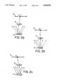
- FIG. 1is a schematic illustration of a preferred embodiment of the invention using a deformable mirror two dimensional modulator.
- FIGS. 2a, 2b, and 2care a schematic illustration of the principle of the invention using a deformable mirror modulator.
- a linear arc lamp 1is powered by power supply 2 and imaged on a deformable mirror array 4 using lens 3.
- the deformable mirror modulator 4is a commercially available device manufactured by Texas Instruments Inc. (Texas) and its principle of operation is covered by U.S. Pat. No. 4,441,791.
- Mirror array 4is imaged onto light sensitive material 6 using lens 5.
- the position of light sensitive material 6is measured by a position transducer 7.
- Position transducer 7is a commercially available unit such as a linear encoder.
- Array 4consists of many rows of deformable mirrors and is positioned in a way that the rows are perpendicular to the direction of motion of material 6.
- the data to be imaged onto material 6is loaded into the first row of array 4 using the driver circuit 8.
- the driver circuitis conventional in nature and is normally a part of the deformable mirror array therefore will not be discussed here.
- a similar circuitis described in U.S. Pat. No. 4,571,603.
- the essence of the inventionis the synchronization between the motion of the light sensitive material 6 and the sequence of transferring the data from row to row inside array 4.
- the dataenters the first row of array 4 and forms a pattern of activated mirrors.
- the same data patternis transferred to the next row while a new pattern is loaded into the first row.
- From the second rowthe data is transferred to the third row without changing the pattern.
- FIG. 2shows the sequence of data transfer between the rows of array 4.
- the number of rowswill be about 100 while the number of mirrors in each row will be about 1000.
- the exact number of rows and number of mirrors per rowis dependent on the dimensions of the light source used and the data rate required.
- the transfer of data between rowsshould occur each time material 6 moved half of 0.01 mm. This is accomplished by using the pulses coming from position transducer 7 to control the data transfer from row to row in array 4.
- moving the material 6is only one of the many known ways of scanning the image of array 4 onto material 6.
- Other well known waysis using a moving mirror to scan the light along material 6 instead of moving the material. In this case position transducer 7 is attached to the moving mirror instead of to material 6.
- Another well known wayis to wrap material 6 around a drum and rotate the drum in front of lens 5. In order to expose all of material 6 normally a two dimensional movement of the material or the light will be required. All these scanning methods do not form part of this invention and are well known to those versed in the art.
- a deformable mirror arrayis not the only two dimensional light modulator which can be used in this invention.
- Other modulators useableare: a two dimensional liquid crystal array, two dimensional magnets-optic modulators, two dimensional ferro-electric modulators and any other modulator which can be fabricated into a two dimensional array.
Landscapes
- Chemical & Material Sciences (AREA)
- Engineering & Computer Science (AREA)
- Manufacturing & Machinery (AREA)
- Materials Engineering (AREA)
- Physics & Mathematics (AREA)
- General Physics & Mathematics (AREA)
- Mechanical Light Control Or Optical Switches (AREA)
- Exposure And Positioning Against Photoresist Photosensitive Materials (AREA)
- Printers Or Recording Devices Using Electromagnetic And Radiation Means (AREA)
- Exposure Or Original Feeding In Electrophotography (AREA)
- Exposure Of Semiconductors, Excluding Electron Or Ion Beam Exposure (AREA)
Abstract
Description
Claims (9)
Priority Applications (5)
| Application Number | Priority Date | Filing Date | Title |
|---|---|---|---|
| US07/546,902US5049901A (en) | 1990-07-02 | 1990-07-02 | Light modulator using large area light sources |
| GB9113707AGB2246644B (en) | 1990-07-02 | 1991-06-25 | Light modulation and exposure system |
| JP15207991AJPH06100829B2 (en) | 1990-07-02 | 1991-06-25 | Optical modulator for large area light source |
| DE4121509ADE4121509A1 (en) | 1990-07-02 | 1991-06-28 | EXPOSURE AND LIGHT MODULATION SYSTEM |
| BE9100623ABE1004579A5 (en) | 1990-07-02 | 1991-07-01 | Light modulator for light sources large area. |
Applications Claiming Priority (1)
| Application Number | Priority Date | Filing Date | Title |
|---|---|---|---|
| US07/546,902US5049901A (en) | 1990-07-02 | 1990-07-02 | Light modulator using large area light sources |
Publications (1)
| Publication Number | Publication Date |
|---|---|
| US5049901Atrue US5049901A (en) | 1991-09-17 |
Family
ID=24182508
Family Applications (1)
| Application Number | Title | Priority Date | Filing Date |
|---|---|---|---|
| US07/546,902Expired - LifetimeUS5049901A (en) | 1990-07-02 | 1990-07-02 | Light modulator using large area light sources |
Country Status (5)
| Country | Link |
|---|---|
| US (1) | US5049901A (en) |
| JP (1) | JPH06100829B2 (en) |
| BE (1) | BE1004579A5 (en) |
| DE (1) | DE4121509A1 (en) |
| GB (1) | GB2246644B (en) |
Cited By (134)
| Publication number | Priority date | Publication date | Assignee | Title |
|---|---|---|---|---|
| WO1992012506A1 (en)* | 1991-01-04 | 1992-07-23 | Rank Brimar Limited | Display device |
| US5208818A (en)* | 1991-12-12 | 1993-05-04 | Creo Products Inc. | Laser system for recording data patterns on a planar substrate |
| EP0556591A1 (en)* | 1992-01-23 | 1993-08-25 | Texas Instruments Incorporated | Printer using an array of deformable mirror devices (DMD) |
| US5247180A (en)* | 1991-12-30 | 1993-09-21 | Texas Instruments Incorporated | Stereolithographic apparatus and method of use |
| EP0687992A1 (en) | 1994-06-16 | 1995-12-20 | Eastman Kodak Company | A light modulator with a laser or laser array for exposing image data |
| EP0640488A3 (en)* | 1993-08-30 | 1996-01-24 | Texas Instruments Inc | Improvements in or relating to printing. |
| DE19545625C1 (en)* | 1995-12-07 | 1997-11-13 | Agfa Gevaert Ag | Method and device for recording images using electronic image signals |
| US5877800A (en)* | 1993-09-10 | 1999-03-02 | Imperial Chemical Industries Plc | Optical data recording apparatus and method |
| US5900981A (en)* | 1997-04-15 | 1999-05-04 | Scitex Corporation Ltd. | Optical system for illuminating a spatial light modulator |
| US5933183A (en)* | 1995-12-12 | 1999-08-03 | Fuji Photo Film Co., Ltd. | Color spatial light modulator and color printer using the same |
| US5966504A (en)* | 1996-03-24 | 1999-10-12 | Scitex Corporation Ltd. | Apparatus and method for printing |
| EP0992350A1 (en) | 1998-10-07 | 2000-04-12 | Barco Graphics N.V. | Method and apparatus for light modulation and exposure at high levels with high resolution |
| US6072518A (en)* | 1997-05-21 | 2000-06-06 | Creo Products Inc. | Method for rapid imaging of thermographic materials by extending exposure time in a single beam laser scanner |
| US6087069A (en)* | 1999-04-16 | 2000-07-11 | Presstek, Inc. | Lithographic imaging and cleaning of printing members having boron ceramic layers |
| US6178006B1 (en)* | 1997-04-18 | 2001-01-23 | Mivatec Hard-Und Software Gmbh | Photoplotting method and an arrangement for plotting a computer-stored raster image on a plane, photosensitive record carrier |
| US6208369B1 (en)* | 1996-08-20 | 2001-03-27 | Creoscitex Corporation Ltd. | Apparatus and method for recording an image |
| WO2001021413A1 (en)* | 1999-09-17 | 2001-03-29 | Basys Print Gmbh Systeme Für Druckindustrie | Device and method for compensating non-uniformities in imaging systems |
| US6222577B1 (en) | 1999-01-26 | 2001-04-24 | Presstek, Inc. | Multiple-beam, diode-pumped imaging system |
| US6268893B1 (en) | 1996-03-11 | 2001-07-31 | American Bank Note Holographics | Method and apparatus for a fringe direct writing system |
| USRE37376E1 (en)* | 1996-08-16 | 2001-09-18 | Creo Products Inc. | Method for rapid imaging of thermographic materials by extending exposure time in a single beam laser scanner |
| EP1155865A3 (en)* | 2000-05-18 | 2002-03-06 | Fuji Photo Film Co., Ltd. | Apparatus for and method of recording image |
| EP0971530A3 (en)* | 1998-07-10 | 2002-05-29 | MIVATEC Hard- und Software GmbH | Photoplotting method for high-energy recording of a computer stored raster image on a light sensitive recording medium |
| US6433934B1 (en) | 2000-08-11 | 2002-08-13 | Yakov Reznichenko | Illumination system for use in imaging systems |
| US6433917B1 (en) | 2000-11-22 | 2002-08-13 | Ball Semiconductor, Inc. | Light modulation device and system |
| US6473237B2 (en) | 2000-11-14 | 2002-10-29 | Ball Semiconductor, Inc. | Point array maskless lithography |
| US6493867B1 (en) | 2000-08-08 | 2002-12-10 | Ball Semiconductor, Inc. | Digital photolithography system for making smooth diagonal components |
| US20030001798A1 (en)* | 2001-06-29 | 2003-01-02 | Asahi Koagku Kogyo Kabushiki Kaisha | Multi-exposure drawing method and apparatus therefor |
| US20030011860A1 (en)* | 2001-07-05 | 2003-01-16 | Asahi Kogaku Kogyo Kabushiki Kaisha | Multi-exposure drawing method and apparatus therefor |
| US6509955B2 (en) | 2000-05-25 | 2003-01-21 | Ball Semiconductor, Inc. | Lens system for maskless photolithography |
| US6512625B2 (en) | 2000-11-22 | 2003-01-28 | Ball Semiconductor, Inc. | Light modulation device and system |
| EP1235421A3 (en)* | 2001-02-27 | 2003-01-29 | Eastman Kodak Company | Method and apparatus for printing high resolution images using multiple reflective spatial light modulators |
| US20030025979A1 (en)* | 2001-07-31 | 2003-02-06 | Ball Semiconductor, Inc. | Surface distortion compensated photolithography |
| US20030026501A1 (en)* | 2001-08-03 | 2003-02-06 | Ball Semiconductor, Inc. | Real time data conversion for a digital display |
| EP1285769A1 (en)* | 2001-08-20 | 2003-02-26 | Eastman Kodak Company | Method and apparatus for printing high resolution images using multiple reflective spatial light modulators |
| US6529262B1 (en) | 1999-04-14 | 2003-03-04 | Ball Semiconductor, Inc. | System and method for performing lithography on a substrate |
| US20030053598A1 (en)* | 2001-09-17 | 2003-03-20 | Fuji Photo Film Co., Ltd. | Image recording method and image recording apparatus |
| US6537738B1 (en) | 2000-08-08 | 2003-03-25 | Ball Semiconductor, Inc. | System and method for making smooth diagonal components with a digital photolithography system |
| EP1322105A1 (en)* | 2001-12-18 | 2003-06-25 | Agfa-Gevaert AG | Device and method to capture a high resolution image in an image plane |
| US6590632B2 (en)* | 2000-10-17 | 2003-07-08 | Fuji Photo Film Co., Ltd. | Image recording method and image recording apparatus |
| EP1193542A3 (en)* | 2000-09-28 | 2003-07-23 | Eastman Kodak Company | A method and apparatus for printing monochromatic images using a spatial light modulator having a selectable light source |
| US20030188650A1 (en)* | 2002-04-09 | 2003-10-09 | Mclean Michael E. | Image replication element and method and system for producing the same |
| US6637329B1 (en) | 2001-05-15 | 2003-10-28 | Creo Products Inc. | Method for improving registration of images on opposing sides of a printing medium |
| US20030214644A1 (en)* | 2002-05-16 | 2003-11-20 | Dainippon Screen Mfg., Co., Ltd. | Pattern writing apparatus and pattern writing method |
| US20030222966A1 (en)* | 2002-05-30 | 2003-12-04 | Dainippon Screen Mfg. Co., Ltd. | Pattern writing apparatus and pattern writing method |
| US6665048B2 (en) | 2002-01-22 | 2003-12-16 | Creo Inc. | Method for imaging a continuously moving object |
| US20030233528A1 (en)* | 2002-06-14 | 2003-12-18 | Ball Semiconductor, Inc. | Modified photolithography movement system |
| US20040004699A1 (en)* | 2002-04-23 | 2004-01-08 | Ball Semiconductor, Inc. | High resolution point array |
| US6700597B2 (en) | 2000-11-14 | 2004-03-02 | Fuji Photo Film Co., Ltd. | Two dimensional scanning image recording method and image recording apparatus with two-dimensionally disposed light source elements |
| US6700598B1 (en) | 2000-04-25 | 2004-03-02 | Cortron Corporation | Digital imaging system employing non-coherent light source |
| US6707591B2 (en) | 2001-04-10 | 2004-03-16 | Silicon Light Machines | Angled illumination for a single order light modulator based projection system |
| US6712480B1 (en) | 2002-09-27 | 2004-03-30 | Silicon Light Machines | Controlled curvature of stressed micro-structures |
| US6714337B1 (en) | 2002-06-28 | 2004-03-30 | Silicon Light Machines | Method and device for modulating a light beam and having an improved gamma response |
| US20040075882A1 (en)* | 2002-08-24 | 2004-04-22 | Meisburger William Daniel | Continuous direct-write optical lithography |
| US6728023B1 (en) | 2002-05-28 | 2004-04-27 | Silicon Light Machines | Optical device arrays with optimized image resolution |
| US6731321B2 (en) | 2001-04-16 | 2004-05-04 | Fuji Photo Film Co., Ltd. | Image recording method and image recording apparatus |
| WO2004034140A3 (en)* | 2002-01-18 | 2004-06-03 | Masanori Kubota | Method and apparatus for high speed digitized exposure |
| US6747781B2 (en) | 2001-06-25 | 2004-06-08 | Silicon Light Machines, Inc. | Method, apparatus, and diffuser for reducing laser speckle |
| US6764875B2 (en) | 1998-07-29 | 2004-07-20 | Silicon Light Machines | Method of and apparatus for sealing an hermetic lid to a semiconductor die |
| US6767751B2 (en) | 2002-05-28 | 2004-07-27 | Silicon Light Machines, Inc. | Integrated driver process flow |
| US20040149767A1 (en)* | 2000-10-06 | 2004-08-05 | Boehm Michael G. | Web burster/inserter |
| US6782205B2 (en) | 2001-06-25 | 2004-08-24 | Silicon Light Machines | Method and apparatus for dynamic equalization in wavelength division multiplexing |
| US6801354B1 (en) | 2002-08-20 | 2004-10-05 | Silicon Light Machines, Inc. | 2-D diffraction grating for substantially eliminating polarization dependent losses |
| US6800238B1 (en) | 2002-01-15 | 2004-10-05 | Silicon Light Machines, Inc. | Method for domain patterning in low coercive field ferroelectrics |
| US20040201832A1 (en)* | 2003-04-10 | 2004-10-14 | Dainippon Screen Mfg. Co., Ltd. | Pattern writing apparatus and pattern writing method |
| US6806997B1 (en) | 2003-02-28 | 2004-10-19 | Silicon Light Machines, Inc. | Patterned diffractive light modulator ribbon for PDL reduction |
| US6813059B2 (en) | 2002-06-28 | 2004-11-02 | Silicon Light Machines, Inc. | Reduced formation of asperities in contact micro-structures |
| US6822797B1 (en) | 2002-05-31 | 2004-11-23 | Silicon Light Machines, Inc. | Light modulator structure for producing high-contrast operation using zero-order light |
| US6829258B1 (en) | 2002-06-26 | 2004-12-07 | Silicon Light Machines, Inc. | Rapidly tunable external cavity laser |
| US6829092B2 (en) | 2001-08-15 | 2004-12-07 | Silicon Light Machines, Inc. | Blazed grating light valve |
| US6829077B1 (en) | 2003-02-28 | 2004-12-07 | Silicon Light Machines, Inc. | Diffractive light modulator with dynamically rotatable diffraction plane |
| US6865346B1 (en) | 2001-06-05 | 2005-03-08 | Silicon Light Machines Corporation | Fiber optic transceiver |
| US6872984B1 (en) | 1998-07-29 | 2005-03-29 | Silicon Light Machines Corporation | Method of sealing a hermetic lid to a semiconductor die at an angle |
| US6886154B2 (en) | 2001-08-08 | 2005-04-26 | Pentax Corporation | Multiple-exposure drawing apparatus and method thereof |
| US6908201B2 (en) | 2002-06-28 | 2005-06-21 | Silicon Light Machines Corporation | Micro-support structures |
| US6922273B1 (en) | 2003-02-28 | 2005-07-26 | Silicon Light Machines Corporation | PDL mitigation structure for diffractive MEMS and gratings |
| US6922272B1 (en) | 2003-02-14 | 2005-07-26 | Silicon Light Machines Corporation | Method and apparatus for leveling thermal stress variations in multi-layer MEMS devices |
| US6927891B1 (en) | 2002-12-23 | 2005-08-09 | Silicon Light Machines Corporation | Tilt-able grating plane for improved crosstalk in 1×N blaze switches |
| US6928207B1 (en) | 2002-12-12 | 2005-08-09 | Silicon Light Machines Corporation | Apparatus for selectively blocking WDM channels |
| US6934070B1 (en) | 2002-12-18 | 2005-08-23 | Silicon Light Machines Corporation | Chirped optical MEM device |
| US6947613B1 (en) | 2003-02-11 | 2005-09-20 | Silicon Light Machines Corporation | Wavelength selective switch and equalizer |
| US6956878B1 (en) | 2000-02-07 | 2005-10-18 | Silicon Light Machines Corporation | Method and apparatus for reducing laser speckle using polarization averaging |
| US6956995B1 (en) | 2001-11-09 | 2005-10-18 | Silicon Light Machines Corporation | Optical communication arrangement |
| US6987600B1 (en) | 2002-12-17 | 2006-01-17 | Silicon Light Machines Corporation | Arbitrary phase profile for better equalization in dynamic gain equalizer |
| US6991953B1 (en) | 2001-09-13 | 2006-01-31 | Silicon Light Machines Corporation | Microelectronic mechanical system and methods |
| US7027202B1 (en) | 2003-02-28 | 2006-04-11 | Silicon Light Machines Corp | Silicon substrate as a light modulator sacrificial layer |
| US7042611B1 (en) | 2003-03-03 | 2006-05-09 | Silicon Light Machines Corporation | Pre-deflected bias ribbons |
| US7054515B1 (en) | 2002-05-30 | 2006-05-30 | Silicon Light Machines Corporation | Diffractive light modulator-based dynamic equalizer with integrated spectral monitor |
| US7057819B1 (en) | 2002-12-17 | 2006-06-06 | Silicon Light Machines Corporation | High contrast tilting ribbon blazed grating |
| US7057795B2 (en) | 2002-08-20 | 2006-06-06 | Silicon Light Machines Corporation | Micro-structures with individually addressable ribbon pairs |
| US7068372B1 (en) | 2003-01-28 | 2006-06-27 | Silicon Light Machines Corporation | MEMS interferometer-based reconfigurable optical add-and-drop multiplexor |
| US20060239588A1 (en)* | 2005-04-01 | 2006-10-26 | 3D Systems, Inc. | Edge smoothness with low resolution projected images for use in solid imaging |
| US20060269217A1 (en)* | 2005-05-31 | 2006-11-30 | Dainippon Screen Mfg. Co., Ltd. | Pattern writing apparatus and block number determining method |
| US7177081B2 (en) | 2001-03-08 | 2007-02-13 | Silicon Light Machines Corporation | High contrast grating light valve type device |
| US20070046771A1 (en)* | 2003-11-03 | 2007-03-01 | Friedrich Luellau | Device and method for digital exposure |
| US20070153080A1 (en)* | 2005-12-29 | 2007-07-05 | Eastman Kodak Company | High-speed continuous film writer |
| US7286764B1 (en) | 2003-02-03 | 2007-10-23 | Silicon Light Machines Corporation | Reconfigurable modulator-based optical add-and-drop multiplexer |
| US20070259066A1 (en)* | 2006-05-03 | 2007-11-08 | 3D Systems, Inc. | Material delivery tension and tracking system for use in solid imaging |
| US20070257055A1 (en)* | 2006-05-03 | 2007-11-08 | 3D Systems, Inc. | Material delivery system for use in solid imaging |
| US20080054531A1 (en)* | 2006-08-29 | 2008-03-06 | 3D Systems, Inc. | Wall Smoothness, Feature Accuracy and Resolution In Projected Images Via Exposure Levels In Solid Imaging |
| EP1664897A4 (en)* | 2003-07-29 | 2008-03-12 | Kodak Graphic Comm Canada Co | Non-uniform light valve |
| US20080124657A1 (en)* | 2005-01-25 | 2008-05-29 | Paul Mayo Holt | Method of Making a Photopolymer Plate |
| US7391973B1 (en) | 2003-02-28 | 2008-06-24 | Silicon Light Machines Corporation | Two-stage gain equalizer |
| US20080169589A1 (en)* | 2007-01-17 | 2008-07-17 | Sperry Charles R | Solid imaging apparatus and method |
| US20080171284A1 (en)* | 2007-01-17 | 2008-07-17 | Hull Charles W | Method for Removing Excess Uncured Build Material in Solid Imaging |
| US20080170112A1 (en)* | 2007-01-17 | 2008-07-17 | Hull Charles W | Build pad, solid image build, and method for building build supports |
| US20080169586A1 (en)* | 2007-01-17 | 2008-07-17 | Hull Charles W | Imager Assembly and Method for Solid Imaging |
| US20080179787A1 (en)* | 2007-01-17 | 2008-07-31 | Sperry Charles R | Elevator and method for tilting solid image build platform for reducing air entrainment and for build release |
| US20080181977A1 (en)* | 2007-01-17 | 2008-07-31 | Sperry Charles R | Brush assembly for removal of excess uncured build material |
| US20080179786A1 (en)* | 2007-01-17 | 2008-07-31 | Sperry Charles R | Cartridge for solid imaging apparatus and method |
| US20080206383A1 (en)* | 2007-01-17 | 2008-08-28 | Hull Charles W | Solid Imaging System with Removal of Excess Uncured Build Material |
| US20080226346A1 (en)* | 2007-01-17 | 2008-09-18 | 3D Systems, Inc. | Inkjet Solid Imaging System and Method for Solid Imaging |
| US20080231731A1 (en)* | 2007-01-17 | 2008-09-25 | Hull Charles W | Imager and method for consistent repeatable alignment in a solid imaging apparatus |
| US20090040485A1 (en)* | 2007-08-10 | 2009-02-12 | Orc Manufacturing Co., Ltd. | Photolithography system |
| US20090101845A1 (en)* | 2005-04-02 | 2009-04-23 | Punch Graphix Prepress Germany Gmbh | Exposure Device for Printing Plates |
| US20090190107A1 (en)* | 2006-05-30 | 2009-07-30 | Paul Mayo Holt | Maskless photopolymer exposure process and apparatus |
| US20100098835A1 (en)* | 2008-10-20 | 2010-04-22 | 3D Systems, Incorporated | Compensation of Actinic Radiation Intensity Profiles for Three-Dimensional Modelers |
| US20100125356A1 (en)* | 2008-11-18 | 2010-05-20 | Global Filtration Systems | System and Method for Manufacturing |
| WO2010131239A1 (en)* | 2009-05-12 | 2010-11-18 | Orbotech Ltd. | Optical imaging system |
| US9034237B2 (en) | 2012-09-25 | 2015-05-19 | 3D Systems, Inc. | Solid imaging systems, components thereof, and methods of solid imaging |
| US9073260B2 (en) | 2011-06-28 | 2015-07-07 | Global Filtration Systems | Apparatus and method for forming three-dimensional objects using linear solidification |
| US9075409B2 (en) | 2011-06-28 | 2015-07-07 | Global Filtration Systems | Apparatus and method for forming three-dimensional objects using linear solidification |
| US9164373B2 (en) | 2013-03-12 | 2015-10-20 | Micronic Mydata AB | Method and device for writing photomasks with reduced mura errors |
| US9354510B2 (en) | 2011-12-16 | 2016-05-31 | Taiwan Semiconductor Manufacturing Company, Ltd. | EUV mask and method for forming the same |
| US9459540B2 (en) | 2013-03-12 | 2016-10-04 | Mycronic AB | Mechanically produced alignment fiducial method and device |
| US9527244B2 (en) | 2014-02-10 | 2016-12-27 | Global Filtration Systems | Apparatus and method for forming three-dimensional objects from solidifiable paste |
| US9586364B2 (en) | 2013-11-27 | 2017-03-07 | Global Filtration Systems | Apparatus and method for forming three-dimensional objects using linear solidification with contourless object data |
| EP3182206A1 (en) | 2015-12-15 | 2017-06-21 | Agfa Graphics NV | Digital print master |
| EP3181357A1 (en) | 2015-12-15 | 2017-06-21 | Agfa Graphics NV | Addiditve manufacturing method using dynamic light projection for flexographic print masters |
| US9902112B2 (en) | 2015-04-07 | 2018-02-27 | Global Filtration Systems | Apparatus and method for forming three-dimensional objects using linear solidification and a vacuum blade |
| US10011076B2 (en) | 2014-02-20 | 2018-07-03 | Global Filtration Systems | Apparatus and method for forming three-dimensional objects using a tilting solidification substrate |
| US10112345B2 (en) | 2013-04-04 | 2018-10-30 | Global Filtration Systems | Apparatus and method for forming three-dimensional objects using linear solidification with travel axis correction and power control |
| US10144205B2 (en) | 2014-02-20 | 2018-12-04 | Global Filtration Systems | Apparatus and method for forming three-dimensional objects using a tilting solidification substrate |
| US10589507B2 (en) | 2013-10-11 | 2020-03-17 | Global Filtration Systems | Apparatus and method for forming three-dimensional objects using a curved build platform or curved solidification substrate |
| US11104117B2 (en) | 2014-02-20 | 2021-08-31 | Global Filtration Systems | Apparatus and method for forming three-dimensional objects using a tilting solidification substrate |
Families Citing this family (11)
| Publication number | Priority date | Publication date | Assignee | Title |
|---|---|---|---|---|
| GB8613465D0 (en)* | 1986-06-04 | 1986-07-09 | Lucas Ind Plc | Fuel pumping apparatus |
| JPH06200857A (en)* | 1993-01-08 | 1994-07-19 | Fuji Heavy Ind Ltd | Fuel pressure control device for high pressure injection type engine |
| DE19545821A1 (en)* | 1995-12-08 | 1997-06-12 | Friedrich Dipl Ing Luellau | Device for exposing printing plates |
| DE19602289A1 (en)* | 1996-01-23 | 1997-07-24 | Roland Man Druckmasch | High resolution print cylinder |
| DE19602307A1 (en)* | 1996-01-23 | 1997-07-24 | Roland Man Druckmasch | Printing machine with coated cylindrical film written by infrared laser |
| CA2275625C (en)* | 1996-12-31 | 2007-01-16 | Claus Mayer | Method and apparatus for controlling a photomechanical exposure device |
| DE19944759A1 (en) | 1999-09-17 | 2001-03-22 | Basys Print Gmbh Systeme Fuer | Procedure for the synchronization of positioning and exposure processes |
| DE10031162A1 (en)* | 2000-06-27 | 2002-01-10 | Heidelberger Druckmasch Ag | System for exposing print form moves image information fed to light switch array in parallel manner to hold image points on print form fixed while illumination head is moved at uniform speed |
| JP2002072491A (en)* | 2000-09-01 | 2002-03-12 | Airex Inc | Printed circuit board manufacturing apparatus |
| DE102007038999A1 (en) | 2007-08-17 | 2009-02-19 | Punch Graphix Prepress Germany Gmbh | Method for increasing throughput and reducing motion blur |
| DE102010046395B4 (en) | 2010-09-24 | 2013-10-24 | Printprocess Ag | exposure assembly |
Citations (3)
| Publication number | Priority date | Publication date | Assignee | Title |
|---|---|---|---|---|
| US4560994A (en)* | 1981-10-08 | 1985-12-24 | Xerox Corporation | Two dimensional electro-optic modulator for printing |
| US4571603A (en)* | 1981-11-03 | 1986-02-18 | Texas Instruments Incorporated | Deformable mirror electrostatic printer |
| US4888724A (en)* | 1986-01-22 | 1989-12-19 | Hughes Aircraft Company | Optical analog data processing systems for handling bipolar and complex data |
Family Cites Families (5)
| Publication number | Priority date | Publication date | Assignee | Title |
|---|---|---|---|---|
| DE2631849A1 (en)* | 1976-07-15 | 1978-01-19 | Agfa Gevaert Ag | RECORDING DEVICE |
| US4360994A (en)* | 1980-12-01 | 1982-11-30 | Hodges Bonnie E | Concrete crack sealing system |
| JPS58103267A (en)* | 1981-12-15 | 1983-06-20 | Fujitsu Ltd | Reading method |
| DE3376728D1 (en)* | 1983-11-01 | 1988-06-23 | Agfa Gevaert Nv | Recording apparatus |
| NL8900238A (en)* | 1989-02-01 | 1990-09-03 | Oce Nederland Bv | METHOD AND APPARATUS FOR IMAGOUS EXPOSURE OF A LIGHT-SENSITIVE MEDIUM USING A NUMBER OF LIGHT-CLOSERS. |
- 1990
- 1990-07-02USUS07/546,902patent/US5049901A/ennot_activeExpired - Lifetime
- 1991
- 1991-06-25JPJP15207991Apatent/JPH06100829B2/ennot_activeExpired - Lifetime
- 1991-06-25GBGB9113707Apatent/GB2246644B/ennot_activeExpired - Fee Related
- 1991-06-28DEDE4121509Apatent/DE4121509A1/ennot_activeWithdrawn
- 1991-07-01BEBE9100623Apatent/BE1004579A5/ennot_activeIP Right Cessation
Patent Citations (3)
| Publication number | Priority date | Publication date | Assignee | Title |
|---|---|---|---|---|
| US4560994A (en)* | 1981-10-08 | 1985-12-24 | Xerox Corporation | Two dimensional electro-optic modulator for printing |
| US4571603A (en)* | 1981-11-03 | 1986-02-18 | Texas Instruments Incorporated | Deformable mirror electrostatic printer |
| US4888724A (en)* | 1986-01-22 | 1989-12-19 | Hughes Aircraft Company | Optical analog data processing systems for handling bipolar and complex data |
Cited By (198)
| Publication number | Priority date | Publication date | Assignee | Title |
|---|---|---|---|---|
| WO1992012506A1 (en)* | 1991-01-04 | 1992-07-23 | Rank Brimar Limited | Display device |
| US5208818A (en)* | 1991-12-12 | 1993-05-04 | Creo Products Inc. | Laser system for recording data patterns on a planar substrate |
| US5247180A (en)* | 1991-12-30 | 1993-09-21 | Texas Instruments Incorporated | Stereolithographic apparatus and method of use |
| EP0556591A1 (en)* | 1992-01-23 | 1993-08-25 | Texas Instruments Incorporated | Printer using an array of deformable mirror devices (DMD) |
| US6061075A (en)* | 1992-01-23 | 2000-05-09 | Texas Instruments Incorporated | Non-systolic time delay and integration printing |
| EP0875386A1 (en)* | 1993-08-30 | 1998-11-04 | Texas Instruments Incorporated | Improvements in or relating to printing |
| EP0640488A3 (en)* | 1993-08-30 | 1996-01-24 | Texas Instruments Inc | Improvements in or relating to printing. |
| US5877800A (en)* | 1993-09-10 | 1999-03-02 | Imperial Chemical Industries Plc | Optical data recording apparatus and method |
| US5521748A (en)* | 1994-06-16 | 1996-05-28 | Eastman Kodak Company | Light modulator with a laser or laser array for exposing image data |
| EP0687992A1 (en) | 1994-06-16 | 1995-12-20 | Eastman Kodak Company | A light modulator with a laser or laser array for exposing image data |
| DE19545625C1 (en)* | 1995-12-07 | 1997-11-13 | Agfa Gevaert Ag | Method and device for recording images using electronic image signals |
| US5933183A (en)* | 1995-12-12 | 1999-08-03 | Fuji Photo Film Co., Ltd. | Color spatial light modulator and color printer using the same |
| US6268893B1 (en) | 1996-03-11 | 2001-07-31 | American Bank Note Holographics | Method and apparatus for a fringe direct writing system |
| US5966504A (en)* | 1996-03-24 | 1999-10-12 | Scitex Corporation Ltd. | Apparatus and method for printing |
| USRE37376E1 (en)* | 1996-08-16 | 2001-09-18 | Creo Products Inc. | Method for rapid imaging of thermographic materials by extending exposure time in a single beam laser scanner |
| US6208369B1 (en)* | 1996-08-20 | 2001-03-27 | Creoscitex Corporation Ltd. | Apparatus and method for recording an image |
| US5969872A (en)* | 1997-04-15 | 1999-10-19 | Scitex Corporation Ltd. | Spatial light modulator illumination system |
| US5900981A (en)* | 1997-04-15 | 1999-05-04 | Scitex Corporation Ltd. | Optical system for illuminating a spatial light modulator |
| US6178006B1 (en)* | 1997-04-18 | 2001-01-23 | Mivatec Hard-Und Software Gmbh | Photoplotting method and an arrangement for plotting a computer-stored raster image on a plane, photosensitive record carrier |
| US6072518A (en)* | 1997-05-21 | 2000-06-06 | Creo Products Inc. | Method for rapid imaging of thermographic materials by extending exposure time in a single beam laser scanner |
| EP0971530A3 (en)* | 1998-07-10 | 2002-05-29 | MIVATEC Hard- und Software GmbH | Photoplotting method for high-energy recording of a computer stored raster image on a light sensitive recording medium |
| US6504567B1 (en) | 1998-07-10 | 2003-01-07 | Mivatec Hard-Und Software Gmbh | Photoplotting process and apparatus for high-energy plotting of a computer-stored raster image on a photosensitive record carrier |
| US6764875B2 (en) | 1998-07-29 | 2004-07-20 | Silicon Light Machines | Method of and apparatus for sealing an hermetic lid to a semiconductor die |
| US6872984B1 (en) | 1998-07-29 | 2005-03-29 | Silicon Light Machines Corporation | Method of sealing a hermetic lid to a semiconductor die at an angle |
| EP0992350A1 (en) | 1998-10-07 | 2000-04-12 | Barco Graphics N.V. | Method and apparatus for light modulation and exposure at high levels with high resolution |
| US6204875B1 (en) | 1998-10-07 | 2001-03-20 | Barco Graphics, Nv | Method and apparatus for light modulation and exposure at high exposure levels with high resolution |
| US6222577B1 (en) | 1999-01-26 | 2001-04-24 | Presstek, Inc. | Multiple-beam, diode-pumped imaging system |
| US6529262B1 (en) | 1999-04-14 | 2003-03-04 | Ball Semiconductor, Inc. | System and method for performing lithography on a substrate |
| US6087069A (en)* | 1999-04-16 | 2000-07-11 | Presstek, Inc. | Lithographic imaging and cleaning of printing members having boron ceramic layers |
| US6965364B1 (en)* | 1999-09-17 | 2005-11-15 | Basys Print GmbH Systeme fuer die Drueckindustrie | Device and method for compensating non-uniformities in imaging systems |
| WO2001021413A1 (en)* | 1999-09-17 | 2001-03-29 | Basys Print Gmbh Systeme Für Druckindustrie | Device and method for compensating non-uniformities in imaging systems |
| US6956878B1 (en) | 2000-02-07 | 2005-10-18 | Silicon Light Machines Corporation | Method and apparatus for reducing laser speckle using polarization averaging |
| US6700598B1 (en) | 2000-04-25 | 2004-03-02 | Cortron Corporation | Digital imaging system employing non-coherent light source |
| EP1155865A3 (en)* | 2000-05-18 | 2002-03-06 | Fuji Photo Film Co., Ltd. | Apparatus for and method of recording image |
| US6529261B2 (en) | 2000-05-18 | 2003-03-04 | Fuji Photo Film Co., Ltd. | Apparatus for and method of recording image |
| US6509955B2 (en) | 2000-05-25 | 2003-01-21 | Ball Semiconductor, Inc. | Lens system for maskless photolithography |
| US6493867B1 (en) | 2000-08-08 | 2002-12-10 | Ball Semiconductor, Inc. | Digital photolithography system for making smooth diagonal components |
| US6537738B1 (en) | 2000-08-08 | 2003-03-25 | Ball Semiconductor, Inc. | System and method for making smooth diagonal components with a digital photolithography system |
| US6433934B1 (en) | 2000-08-11 | 2002-08-13 | Yakov Reznichenko | Illumination system for use in imaging systems |
| EP1193542A3 (en)* | 2000-09-28 | 2003-07-23 | Eastman Kodak Company | A method and apparatus for printing monochromatic images using a spatial light modulator having a selectable light source |
| US20040149767A1 (en)* | 2000-10-06 | 2004-08-05 | Boehm Michael G. | Web burster/inserter |
| US6590632B2 (en)* | 2000-10-17 | 2003-07-08 | Fuji Photo Film Co., Ltd. | Image recording method and image recording apparatus |
| US6473237B2 (en) | 2000-11-14 | 2002-10-29 | Ball Semiconductor, Inc. | Point array maskless lithography |
| US6700597B2 (en) | 2000-11-14 | 2004-03-02 | Fuji Photo Film Co., Ltd. | Two dimensional scanning image recording method and image recording apparatus with two-dimensionally disposed light source elements |
| US6512625B2 (en) | 2000-11-22 | 2003-01-28 | Ball Semiconductor, Inc. | Light modulation device and system |
| US6433917B1 (en) | 2000-11-22 | 2002-08-13 | Ball Semiconductor, Inc. | Light modulation device and system |
| EP1235421A3 (en)* | 2001-02-27 | 2003-01-29 | Eastman Kodak Company | Method and apparatus for printing high resolution images using multiple reflective spatial light modulators |
| US7177081B2 (en) | 2001-03-08 | 2007-02-13 | Silicon Light Machines Corporation | High contrast grating light valve type device |
| US6707591B2 (en) | 2001-04-10 | 2004-03-16 | Silicon Light Machines | Angled illumination for a single order light modulator based projection system |
| US6731321B2 (en) | 2001-04-16 | 2004-05-04 | Fuji Photo Film Co., Ltd. | Image recording method and image recording apparatus |
| US6637329B1 (en) | 2001-05-15 | 2003-10-28 | Creo Products Inc. | Method for improving registration of images on opposing sides of a printing medium |
| US6865346B1 (en) | 2001-06-05 | 2005-03-08 | Silicon Light Machines Corporation | Fiber optic transceiver |
| US6782205B2 (en) | 2001-06-25 | 2004-08-24 | Silicon Light Machines | Method and apparatus for dynamic equalization in wavelength division multiplexing |
| US6747781B2 (en) | 2001-06-25 | 2004-06-08 | Silicon Light Machines, Inc. | Method, apparatus, and diffuser for reducing laser speckle |
| US7336391B2 (en) | 2001-06-29 | 2008-02-26 | Orc Manufacturing Co., Ltd. | Multi-exposure drawing method and apparatus therefor |
| US20030001798A1 (en)* | 2001-06-29 | 2003-01-02 | Asahi Koagku Kogyo Kabushiki Kaisha | Multi-exposure drawing method and apparatus therefor |
| US7136087B2 (en) | 2001-07-05 | 2006-11-14 | Orc Manufacturing Co., Ltd. | Multi-exposure drawing method and apparatus therefor |
| US20030011860A1 (en)* | 2001-07-05 | 2003-01-16 | Asahi Kogaku Kogyo Kabushiki Kaisha | Multi-exposure drawing method and apparatus therefor |
| US20030025979A1 (en)* | 2001-07-31 | 2003-02-06 | Ball Semiconductor, Inc. | Surface distortion compensated photolithography |
| US6965387B2 (en) | 2001-08-03 | 2005-11-15 | Ball Semiconductor, Inc. | Real time data conversion for a digital display |
| US20030026501A1 (en)* | 2001-08-03 | 2003-02-06 | Ball Semiconductor, Inc. | Real time data conversion for a digital display |
| US6886154B2 (en) | 2001-08-08 | 2005-04-26 | Pentax Corporation | Multiple-exposure drawing apparatus and method thereof |
| US6829092B2 (en) | 2001-08-15 | 2004-12-07 | Silicon Light Machines, Inc. | Blazed grating light valve |
| EP1285769A1 (en)* | 2001-08-20 | 2003-02-26 | Eastman Kodak Company | Method and apparatus for printing high resolution images using multiple reflective spatial light modulators |
| US6991953B1 (en) | 2001-09-13 | 2006-01-31 | Silicon Light Machines Corporation | Microelectronic mechanical system and methods |
| US7049164B2 (en) | 2001-09-13 | 2006-05-23 | Silicon Light Machines Corporation | Microelectronic mechanical system and methods |
| EP1293348A3 (en)* | 2001-09-17 | 2003-04-23 | Fuji Photo Film Co., Ltd. | Image recording method and image recording apparatus |
| US20030053598A1 (en)* | 2001-09-17 | 2003-03-20 | Fuji Photo Film Co., Ltd. | Image recording method and image recording apparatus |
| US7212225B2 (en) | 2001-09-17 | 2007-05-01 | Fujifilm Corporation | Enhanced resolution image recording method and enhanced resolution image recording apparatus |
| US6956995B1 (en) | 2001-11-09 | 2005-10-18 | Silicon Light Machines Corporation | Optical communication arrangement |
| EP1322105A1 (en)* | 2001-12-18 | 2003-06-25 | Agfa-Gevaert AG | Device and method to capture a high resolution image in an image plane |
| US6800238B1 (en) | 2002-01-15 | 2004-10-05 | Silicon Light Machines, Inc. | Method for domain patterning in low coercive field ferroelectrics |
| WO2004034140A3 (en)* | 2002-01-18 | 2004-06-03 | Masanori Kubota | Method and apparatus for high speed digitized exposure |
| US6665048B2 (en) | 2002-01-22 | 2003-12-16 | Creo Inc. | Method for imaging a continuously moving object |
| US6976426B2 (en)* | 2002-04-09 | 2005-12-20 | Day International, Inc. | Image replication element and method and system for producing the same |
| US20030188650A1 (en)* | 2002-04-09 | 2003-10-09 | Mclean Michael E. | Image replication element and method and system for producing the same |
| US20040004699A1 (en)* | 2002-04-23 | 2004-01-08 | Ball Semiconductor, Inc. | High resolution point array |
| US6870604B2 (en)* | 2002-04-23 | 2005-03-22 | Ball Semiconductor, Inc. | High resolution point array |
| US6903798B2 (en) | 2002-05-16 | 2005-06-07 | Dainippon Screen Mfg. Co., Ltd. | Pattern writing apparatus and pattern writing method |
| US20050002002A1 (en)* | 2002-05-16 | 2005-01-06 | Dainippon Screen Mfg. Co., Ltd | Pattern writing apparatus and pattern writing method |
| US20030214644A1 (en)* | 2002-05-16 | 2003-11-20 | Dainippon Screen Mfg., Co., Ltd. | Pattern writing apparatus and pattern writing method |
| US6767751B2 (en) | 2002-05-28 | 2004-07-27 | Silicon Light Machines, Inc. | Integrated driver process flow |
| US6728023B1 (en) | 2002-05-28 | 2004-04-27 | Silicon Light Machines | Optical device arrays with optimized image resolution |
| US20030222966A1 (en)* | 2002-05-30 | 2003-12-04 | Dainippon Screen Mfg. Co., Ltd. | Pattern writing apparatus and pattern writing method |
| US7054515B1 (en) | 2002-05-30 | 2006-05-30 | Silicon Light Machines Corporation | Diffractive light modulator-based dynamic equalizer with integrated spectral monitor |
| US6859223B2 (en) | 2002-05-30 | 2005-02-22 | Dainippon Screen Mfg. Co., Ltd. | Pattern writing apparatus and pattern writing method |
| US6822797B1 (en) | 2002-05-31 | 2004-11-23 | Silicon Light Machines, Inc. | Light modulator structure for producing high-contrast operation using zero-order light |
| US7164961B2 (en) | 2002-06-14 | 2007-01-16 | Disco Corporation | Modified photolithography movement system |
| US20030233528A1 (en)* | 2002-06-14 | 2003-12-18 | Ball Semiconductor, Inc. | Modified photolithography movement system |
| US6829258B1 (en) | 2002-06-26 | 2004-12-07 | Silicon Light Machines, Inc. | Rapidly tunable external cavity laser |
| US6908201B2 (en) | 2002-06-28 | 2005-06-21 | Silicon Light Machines Corporation | Micro-support structures |
| US6813059B2 (en) | 2002-06-28 | 2004-11-02 | Silicon Light Machines, Inc. | Reduced formation of asperities in contact micro-structures |
| US6714337B1 (en) | 2002-06-28 | 2004-03-30 | Silicon Light Machines | Method and device for modulating a light beam and having an improved gamma response |
| US7057795B2 (en) | 2002-08-20 | 2006-06-06 | Silicon Light Machines Corporation | Micro-structures with individually addressable ribbon pairs |
| US6801354B1 (en) | 2002-08-20 | 2004-10-05 | Silicon Light Machines, Inc. | 2-D diffraction grating for substantially eliminating polarization dependent losses |
| US7719753B2 (en) | 2002-08-24 | 2010-05-18 | Maskless Lithography, Inc. | Method of operation for SLM-based optical lithography tool |
| US20090086176A1 (en)* | 2002-08-24 | 2009-04-02 | Maskless Lithography, Inc. | Method of operation for slm-based optical lithography tool |
| US20090086182A1 (en)* | 2002-08-24 | 2009-04-02 | Maskless Lithography, Inc. | Apparatus for slm-based optical lithography with gray level capability |
| US7167296B2 (en) | 2002-08-24 | 2007-01-23 | Maskless Lithography, Inc. | Continuous direct-write optical lithography |
| US20050041229A1 (en)* | 2002-08-24 | 2005-02-24 | Meisburger William Daniel | Continuous direct-write optical lithography |
| US7295362B2 (en) | 2002-08-24 | 2007-11-13 | Maskless Lithography, Inc. | Continuous direct-write optical lithography |
| US7639416B2 (en) | 2002-08-24 | 2009-12-29 | Maskless Lithography, Inc. | Apparatus for SLM-based optical lithography with gray level capability |
| US7508570B1 (en) | 2002-08-24 | 2009-03-24 | Maskless Lithography, Inc. | Gray level method for slim-based optical lithography |
| US20090086307A1 (en)* | 2002-08-24 | 2009-04-02 | Maskless Lithography, Inc. | Gray level method for slm-based optical lithography |
| US20040075882A1 (en)* | 2002-08-24 | 2004-04-22 | Meisburger William Daniel | Continuous direct-write optical lithography |
| US6712480B1 (en) | 2002-09-27 | 2004-03-30 | Silicon Light Machines | Controlled curvature of stressed micro-structures |
| US6928207B1 (en) | 2002-12-12 | 2005-08-09 | Silicon Light Machines Corporation | Apparatus for selectively blocking WDM channels |
| US7057819B1 (en) | 2002-12-17 | 2006-06-06 | Silicon Light Machines Corporation | High contrast tilting ribbon blazed grating |
| US6987600B1 (en) | 2002-12-17 | 2006-01-17 | Silicon Light Machines Corporation | Arbitrary phase profile for better equalization in dynamic gain equalizer |
| US6934070B1 (en) | 2002-12-18 | 2005-08-23 | Silicon Light Machines Corporation | Chirped optical MEM device |
| US6927891B1 (en) | 2002-12-23 | 2005-08-09 | Silicon Light Machines Corporation | Tilt-able grating plane for improved crosstalk in 1×N blaze switches |
| US7068372B1 (en) | 2003-01-28 | 2006-06-27 | Silicon Light Machines Corporation | MEMS interferometer-based reconfigurable optical add-and-drop multiplexor |
| US7286764B1 (en) | 2003-02-03 | 2007-10-23 | Silicon Light Machines Corporation | Reconfigurable modulator-based optical add-and-drop multiplexer |
| US6947613B1 (en) | 2003-02-11 | 2005-09-20 | Silicon Light Machines Corporation | Wavelength selective switch and equalizer |
| US6922272B1 (en) | 2003-02-14 | 2005-07-26 | Silicon Light Machines Corporation | Method and apparatus for leveling thermal stress variations in multi-layer MEMS devices |
| US7391973B1 (en) | 2003-02-28 | 2008-06-24 | Silicon Light Machines Corporation | Two-stage gain equalizer |
| US6922273B1 (en) | 2003-02-28 | 2005-07-26 | Silicon Light Machines Corporation | PDL mitigation structure for diffractive MEMS and gratings |
| US6806997B1 (en) | 2003-02-28 | 2004-10-19 | Silicon Light Machines, Inc. | Patterned diffractive light modulator ribbon for PDL reduction |
| US7027202B1 (en) | 2003-02-28 | 2006-04-11 | Silicon Light Machines Corp | Silicon substrate as a light modulator sacrificial layer |
| US6829077B1 (en) | 2003-02-28 | 2004-12-07 | Silicon Light Machines, Inc. | Diffractive light modulator with dynamically rotatable diffraction plane |
| US7042611B1 (en) | 2003-03-03 | 2006-05-09 | Silicon Light Machines Corporation | Pre-deflected bias ribbons |
| US20040201832A1 (en)* | 2003-04-10 | 2004-10-14 | Dainippon Screen Mfg. Co., Ltd. | Pattern writing apparatus and pattern writing method |
| US7190435B2 (en) | 2003-04-10 | 2007-03-13 | Dainippon Screen Mfg. Co., Ltd. | Pattern writing apparatus and pattern writing method |
| KR101045703B1 (en) | 2003-07-29 | 2011-06-30 | 코닥 그래픽 커뮤니케이션즈 캐나다 캄파니 | Optical valves and manufacturing methods thereof, imaging methods and systems |
| EP1664897A4 (en)* | 2003-07-29 | 2008-03-12 | Kodak Graphic Comm Canada Co | Non-uniform light valve |
| US20070046771A1 (en)* | 2003-11-03 | 2007-03-01 | Friedrich Luellau | Device and method for digital exposure |
| US8547592B2 (en)* | 2003-11-03 | 2013-10-01 | Xeikon Ip Bv | Device and method for digital exposure |
| US20080124657A1 (en)* | 2005-01-25 | 2008-05-29 | Paul Mayo Holt | Method of Making a Photopolymer Plate |
| US8703037B2 (en) | 2005-04-01 | 2014-04-22 | 3D Systems, Inc. | Edge smoothness with low resolution projected images for use in solid imaging |
| US7758799B2 (en) | 2005-04-01 | 2010-07-20 | 3D Systems, Inc. | Edge smoothness with low resolution projected images for use in solid imaging |
| US20060239588A1 (en)* | 2005-04-01 | 2006-10-26 | 3D Systems, Inc. | Edge smoothness with low resolution projected images for use in solid imaging |
| US20090101845A1 (en)* | 2005-04-02 | 2009-04-23 | Punch Graphix Prepress Germany Gmbh | Exposure Device for Printing Plates |
| US20060269217A1 (en)* | 2005-05-31 | 2006-11-30 | Dainippon Screen Mfg. Co., Ltd. | Pattern writing apparatus and block number determining method |
| US7268856B2 (en) | 2005-05-31 | 2007-09-11 | Dainippon Screen Mfg. Co., Ltd. | Pattern writing apparatus and block number determining method |
| US20070153080A1 (en)* | 2005-12-29 | 2007-07-05 | Eastman Kodak Company | High-speed continuous film writer |
| US7931460B2 (en) | 2006-05-03 | 2011-04-26 | 3D Systems, Inc. | Material delivery system for use in solid imaging |
| US20090110763A1 (en)* | 2006-05-03 | 2009-04-30 | 3D Systems, Inc. | Material Delivery Tension and Tracking System for Use in Solid Imaging |
| US20070257055A1 (en)* | 2006-05-03 | 2007-11-08 | 3D Systems, Inc. | Material delivery system for use in solid imaging |
| US7467939B2 (en) | 2006-05-03 | 2008-12-23 | 3D Systems, Inc. | Material delivery tension and tracking system for use in solid imaging |
| US20070259066A1 (en)* | 2006-05-03 | 2007-11-08 | 3D Systems, Inc. | Material delivery tension and tracking system for use in solid imaging |
| US8114569B2 (en) | 2006-05-30 | 2012-02-14 | Photocentric Limited | Maskless photopolymer exposure process and apparatus |
| US20090190107A1 (en)* | 2006-05-30 | 2009-07-30 | Paul Mayo Holt | Maskless photopolymer exposure process and apparatus |
| US9415544B2 (en) | 2006-08-29 | 2016-08-16 | 3D Systems, Inc. | Wall smoothness, feature accuracy and resolution in projected images via exposure levels in solid imaging |
| US20080054531A1 (en)* | 2006-08-29 | 2008-03-06 | 3D Systems, Inc. | Wall Smoothness, Feature Accuracy and Resolution In Projected Images Via Exposure Levels In Solid Imaging |
| US20080226346A1 (en)* | 2007-01-17 | 2008-09-18 | 3D Systems, Inc. | Inkjet Solid Imaging System and Method for Solid Imaging |
| US8221671B2 (en) | 2007-01-17 | 2012-07-17 | 3D Systems, Inc. | Imager and method for consistent repeatable alignment in a solid imaging apparatus |
| US7614866B2 (en) | 2007-01-17 | 2009-11-10 | 3D Systems, Inc. | Solid imaging apparatus and method |
| US20080231731A1 (en)* | 2007-01-17 | 2008-09-25 | Hull Charles W | Imager and method for consistent repeatable alignment in a solid imaging apparatus |
| US20080169589A1 (en)* | 2007-01-17 | 2008-07-17 | Sperry Charles R | Solid imaging apparatus and method |
| US7706910B2 (en) | 2007-01-17 | 2010-04-27 | 3D Systems, Inc. | Imager assembly and method for solid imaging |
| US20080206383A1 (en)* | 2007-01-17 | 2008-08-28 | Hull Charles W | Solid Imaging System with Removal of Excess Uncured Build Material |
| US20080171284A1 (en)* | 2007-01-17 | 2008-07-17 | Hull Charles W | Method for Removing Excess Uncured Build Material in Solid Imaging |
| US7731887B2 (en) | 2007-01-17 | 2010-06-08 | 3D Systems, Inc. | Method for removing excess uncured build material in solid imaging |
| US20080179786A1 (en)* | 2007-01-17 | 2008-07-31 | Sperry Charles R | Cartridge for solid imaging apparatus and method |
| US7771183B2 (en) | 2007-01-17 | 2010-08-10 | 3D Systems, Inc. | Solid imaging system with removal of excess uncured build material |
| US20080170112A1 (en)* | 2007-01-17 | 2008-07-17 | Hull Charles W | Build pad, solid image build, and method for building build supports |
| US20080181977A1 (en)* | 2007-01-17 | 2008-07-31 | Sperry Charles R | Brush assembly for removal of excess uncured build material |
| US20080179787A1 (en)* | 2007-01-17 | 2008-07-31 | Sperry Charles R | Elevator and method for tilting solid image build platform for reducing air entrainment and for build release |
| US8003039B2 (en) | 2007-01-17 | 2011-08-23 | 3D Systems, Inc. | Method for tilting solid image build platform for reducing air entrainment and for build release |
| US8465689B2 (en) | 2007-01-17 | 2013-06-18 | 3D Systems, Inc. | Elevator and method for tilting solid image build platform for reducing air entrainment and for build release |
| US8105066B2 (en) | 2007-01-17 | 2012-01-31 | 3D Systems, Inc. | Cartridge for solid imaging apparatus and method |
| US20080169586A1 (en)* | 2007-01-17 | 2008-07-17 | Hull Charles W | Imager Assembly and Method for Solid Imaging |
| US20090040485A1 (en)* | 2007-08-10 | 2009-02-12 | Orc Manufacturing Co., Ltd. | Photolithography system |
| US8599357B2 (en)* | 2007-08-10 | 2013-12-03 | Orc Manufacturing Co., Ltd. | Photolithography system |
| US8048359B2 (en) | 2008-10-20 | 2011-11-01 | 3D Systems, Inc. | Compensation of actinic radiation intensity profiles for three-dimensional modelers |
| US8568646B2 (en) | 2008-10-20 | 2013-10-29 | 3D Systems, Inc. | Compensation of actinic radiation intensity profiles for three-dimensional modelers |
| US20100098835A1 (en)* | 2008-10-20 | 2010-04-22 | 3D Systems, Incorporated | Compensation of Actinic Radiation Intensity Profiles for Three-Dimensional Modelers |
| US8666142B2 (en) | 2008-11-18 | 2014-03-04 | Global Filtration Systems | System and method for manufacturing |
| US20100125356A1 (en)* | 2008-11-18 | 2010-05-20 | Global Filtration Systems | System and Method for Manufacturing |
| CN102414025A (en)* | 2009-05-12 | 2012-04-11 | 奥博泰克有限公司 | Optical imaging system |
| WO2010131239A1 (en)* | 2009-05-12 | 2010-11-18 | Orbotech Ltd. | Optical imaging system |
| US9075409B2 (en) | 2011-06-28 | 2015-07-07 | Global Filtration Systems | Apparatus and method for forming three-dimensional objects using linear solidification |
| US9073260B2 (en) | 2011-06-28 | 2015-07-07 | Global Filtration Systems | Apparatus and method for forming three-dimensional objects using linear solidification |
| US9073262B2 (en) | 2011-06-28 | 2015-07-07 | Global Filtration Systems | Apparatus and method for forming three-dimensional objects using linear solidification |
| US9073261B2 (en) | 2011-06-28 | 2015-07-07 | Global Filtration Systems | Apparatus and method for forming three-dimensional objects using linear solidification |
| US9079355B2 (en) | 2011-06-28 | 2015-07-14 | Global Filtration Systems | Apparatus and method for forming three-dimensional objects using linear solidification |
| US10000023B2 (en) | 2011-06-28 | 2018-06-19 | Global Filtration Systems | Apparatus and method for forming three-dimensional objects using linear solidification |
| US9981425B2 (en) | 2011-06-28 | 2018-05-29 | Global Filtration Systems | Apparatus and method for forming three-dimensional objects using linear solidification |
| US9354510B2 (en) | 2011-12-16 | 2016-05-31 | Taiwan Semiconductor Manufacturing Company, Ltd. | EUV mask and method for forming the same |
| US9034237B2 (en) | 2012-09-25 | 2015-05-19 | 3D Systems, Inc. | Solid imaging systems, components thereof, and methods of solid imaging |
| US9164373B2 (en) | 2013-03-12 | 2015-10-20 | Micronic Mydata AB | Method and device for writing photomasks with reduced mura errors |
| US9459540B2 (en) | 2013-03-12 | 2016-10-04 | Mycronic AB | Mechanically produced alignment fiducial method and device |
| US10112345B2 (en) | 2013-04-04 | 2018-10-30 | Global Filtration Systems | Apparatus and method for forming three-dimensional objects using linear solidification with travel axis correction and power control |
| US10589507B2 (en) | 2013-10-11 | 2020-03-17 | Global Filtration Systems | Apparatus and method for forming three-dimensional objects using a curved build platform or curved solidification substrate |
| US9586364B2 (en) | 2013-11-27 | 2017-03-07 | Global Filtration Systems | Apparatus and method for forming three-dimensional objects using linear solidification with contourless object data |
| US10005237B2 (en) | 2013-11-27 | 2018-06-26 | Global Filtration Systems | Apparatus and method for forming three-dimensional objects using linear solidification with contourless object data |
| US9527244B2 (en) | 2014-02-10 | 2016-12-27 | Global Filtration Systems | Apparatus and method for forming three-dimensional objects from solidifiable paste |
| US9975296B2 (en) | 2014-02-10 | 2018-05-22 | Global Filtration Systems | Apparatus and method for forming three-dimensional objects from solidifiable paste |
| US10011076B2 (en) | 2014-02-20 | 2018-07-03 | Global Filtration Systems | Apparatus and method for forming three-dimensional objects using a tilting solidification substrate |
| US10144205B2 (en) | 2014-02-20 | 2018-12-04 | Global Filtration Systems | Apparatus and method for forming three-dimensional objects using a tilting solidification substrate |
| US10300663B2 (en) | 2014-02-20 | 2019-05-28 | Global Filtration Systems | Apparatus and method for forming three-dimensional objects using a tilting solidification substrate |
| US11104117B2 (en) | 2014-02-20 | 2021-08-31 | Global Filtration Systems | Apparatus and method for forming three-dimensional objects using a tilting solidification substrate |
| US9902112B2 (en) | 2015-04-07 | 2018-02-27 | Global Filtration Systems | Apparatus and method for forming three-dimensional objects using linear solidification and a vacuum blade |
| WO2017102353A1 (en) | 2015-12-15 | 2017-06-22 | Agfa Graphics Nv | Additive manufacturing method using dynamic light projection for flexographic print masters |
| EP3181357A1 (en) | 2015-12-15 | 2017-06-21 | Agfa Graphics NV | Addiditve manufacturing method using dynamic light projection for flexographic print masters |
| US10457081B2 (en) | 2015-12-15 | 2019-10-29 | Agfa Nv | Additive manufacturing method using dynamic light projection for flexographic print masters |
| EP3608721A1 (en) | 2015-12-15 | 2020-02-12 | Agfa Nv | System for making a flexographic print master |
| EP3182206A1 (en) | 2015-12-15 | 2017-06-21 | Agfa Graphics NV | Digital print master |
Also Published As
| Publication number | Publication date |
|---|---|
| GB2246644B (en) | 1994-10-26 |
| JPH06100829B2 (en) | 1994-12-12 |
| BE1004579A5 (en) | 1992-12-15 |
| GB2246644A (en) | 1992-02-05 |
| JPH05341630A (en) | 1993-12-24 |
| DE4121509A1 (en) | 1992-01-09 |
| GB9113707D0 (en) | 1991-08-14 |
Similar Documents
| Publication | Publication Date | Title |
|---|---|---|
| US5049901A (en) | Light modulator using large area light sources | |
| US5521748A (en) | Light modulator with a laser or laser array for exposing image data | |
| US5132723A (en) | Method and apparatus for exposure control in light valves | |
| EP0620676B1 (en) | Process for digital micromirror printer | |
| EP0556591A1 (en) | Printer using an array of deformable mirror devices (DMD) | |
| US20030214644A1 (en) | Pattern writing apparatus and pattern writing method | |
| US5684620A (en) | High resolution imaging system and method of imaging using the same | |
| US5923359A (en) | Internal drum scophony raster recording device | |
| US6590632B2 (en) | Image recording method and image recording apparatus | |
| US6862108B2 (en) | Optical printer with micromirror device | |
| US6734889B2 (en) | Color printer comprising a linear grating spatial light modulator | |
| JP2001305664A (en) | Printer | |
| US5117245A (en) | Electronic printer or scanner using a fiber optic bundle and an array light emission device | |
| US5548408A (en) | Image processing system | |
| US6148134A (en) | Fiber mounts for fiber optic harness in a fiber optic-based imaging system | |
| RU2178907C2 (en) | System for carrying images converted into digital form onto sensitive base | |
| US5721609A (en) | Exposure apparatus with a PLZT shutter which received light from a projecting means capable of sequentially generating red, blue and green light | |
| USRE38297E1 (en) | Internal drum scophony raster recording device | |
| US7907249B2 (en) | Film exposer and method for exposing light-sensitive films | |
| JPH02221920A (en) | Method and apparatus for simultaneous writing into a plurality of lalc cells by laser | |
| JPS6259462A (en) | Semiconductor laser scanner | |
| WO2000059207A1 (en) | Light distribution device for fiber optic-based imaging system | |
| JP2001287403A (en) | Printer | |
| JP2001322306A (en) | System and method for exposing recording medium in imaging system | |
| JP2004050483A (en) | Image exposing system and image exposing method |
Legal Events
| Date | Code | Title | Description |
|---|---|---|---|
| AS | Assignment | Owner name:CREO PRODUCTS INC. Free format text:ASSIGNMENT OF ASSIGNORS INTEREST.;ASSIGNOR:GELBART, DANIEL;REEL/FRAME:005709/0112 Effective date:19910426 | |
| STCF | Information on status: patent grant | Free format text:PATENTED CASE | |
| FEPP | Fee payment procedure | Free format text:PAYER NUMBER DE-ASSIGNED (ORIGINAL EVENT CODE: RMPN); ENTITY STATUS OF PATENT OWNER: LARGE ENTITY Free format text:PAYOR NUMBER ASSIGNED (ORIGINAL EVENT CODE: ASPN); ENTITY STATUS OF PATENT OWNER: LARGE ENTITY | |
| FPAY | Fee payment | Year of fee payment:4 | |
| FEPP | Fee payment procedure | Free format text:PAT HLDR NO LONGER CLAIMS SMALL ENT STAT AS SMALL BUSINESS (ORIGINAL EVENT CODE: LSM2); ENTITY STATUS OF PATENT OWNER: LARGE ENTITY | |
| REMI | Maintenance fee reminder mailed | ||
| FPAY | Fee payment | Year of fee payment:8 | |
| SULP | Surcharge for late payment | ||
| FPAY | Fee payment | Year of fee payment:12 | |
| SULP | Surcharge for late payment | Year of fee payment:11 | |
| AS | Assignment | Owner name:KODAK GRAPHIC COMMUNICATIONS CANADA COMPANY, CANAD Free format text:CERTIFICATE OF AMALGAMATION;ASSIGNOR:CREO INC. (FORMERLY KNOWNS AS CREO PRODUCTS INC.);REEL/FRAME:017846/0512 Effective date:20051001 |