US5046953A - Method and apparatus for mounting an integrated circuit on a printed circuit board - Google Patents
Method and apparatus for mounting an integrated circuit on a printed circuit boardDownload PDFInfo
- Publication number
- US5046953A US5046953AUS07/529,069US52906990AUS5046953AUS 5046953 AUS5046953 AUS 5046953AUS 52906990 AUS52906990 AUS 52906990AUS 5046953 AUS5046953 AUS 5046953A
- Authority
- US
- United States
- Prior art keywords
- tab segment
- circuit board
- sheet
- tab
- leads
- Prior art date
- Legal status (The legal status is an assumption and is not a legal conclusion. Google has not performed a legal analysis and makes no representation as to the accuracy of the status listed.)
- Expired - Lifetime
Links
Images


Classifications
- H—ELECTRICITY
- H01—ELECTRIC ELEMENTS
- H01R—ELECTRICALLY-CONDUCTIVE CONNECTIONS; STRUCTURAL ASSOCIATIONS OF A PLURALITY OF MUTUALLY-INSULATED ELECTRICAL CONNECTING ELEMENTS; COUPLING DEVICES; CURRENT COLLECTORS
- H01R13/00—Details of coupling devices of the kinds covered by groups H01R12/70 or H01R24/00 - H01R33/00
- H01R13/02—Contact members
- H01R13/22—Contacts for co-operating by abutting
- H01R13/24—Contacts for co-operating by abutting resilient; resiliently-mounted
- H01R13/2407—Contacts for co-operating by abutting resilient; resiliently-mounted characterized by the resilient means
- H01R13/2414—Contacts for co-operating by abutting resilient; resiliently-mounted characterized by the resilient means conductive elastomers
- H—ELECTRICITY
- H01—ELECTRIC ELEMENTS
- H01R—ELECTRICALLY-CONDUCTIVE CONNECTIONS; STRUCTURAL ASSOCIATIONS OF A PLURALITY OF MUTUALLY-INSULATED ELECTRICAL CONNECTING ELEMENTS; COUPLING DEVICES; CURRENT COLLECTORS
- H01R12/00—Structural associations of a plurality of mutually-insulated electrical connecting elements, specially adapted for printed circuits, e.g. printed circuit boards [PCB], flat or ribbon cables, or like generally planar structures, e.g. terminal strips, terminal blocks; Coupling devices specially adapted for printed circuits, flat or ribbon cables, or like generally planar structures; Terminals specially adapted for contact with, or insertion into, printed circuits, flat or ribbon cables, or like generally planar structures
- H01R12/70—Coupling devices
- H01R12/71—Coupling devices for rigid printing circuits or like structures
- H01R12/712—Coupling devices for rigid printing circuits or like structures co-operating with the surface of the printed circuit or with a coupling device exclusively provided on the surface of the printed circuit
- H01R12/714—Coupling devices for rigid printing circuits or like structures co-operating with the surface of the printed circuit or with a coupling device exclusively provided on the surface of the printed circuit with contacts abutting directly the printed circuit; Button contacts therefore provided on the printed circuit
- H—ELECTRICITY
- H05—ELECTRIC TECHNIQUES NOT OTHERWISE PROVIDED FOR
- H05K—PRINTED CIRCUITS; CASINGS OR CONSTRUCTIONAL DETAILS OF ELECTRIC APPARATUS; MANUFACTURE OF ASSEMBLAGES OF ELECTRICAL COMPONENTS
- H05K3/00—Apparatus or processes for manufacturing printed circuits
- H05K3/30—Assembling printed circuits with electric components, e.g. with resistor
- H05K3/32—Assembling printed circuits with electric components, e.g. with resistor electrically connecting electric components or wires to printed circuits
- H05K3/325—Assembling printed circuits with electric components, e.g. with resistor electrically connecting electric components or wires to printed circuits by abutting or pinching, i.e. without alloying process; mechanical auxiliary parts therefor
- H—ELECTRICITY
- H05—ELECTRIC TECHNIQUES NOT OTHERWISE PROVIDED FOR
- H05K—PRINTED CIRCUITS; CASINGS OR CONSTRUCTIONAL DETAILS OF ELECTRIC APPARATUS; MANUFACTURE OF ASSEMBLAGES OF ELECTRICAL COMPONENTS
- H05K2201/00—Indexing scheme relating to printed circuits covered by H05K1/00
- H05K2201/10—Details of components or other objects attached to or integrated in a printed circuit board
- H05K2201/10227—Other objects, e.g. metallic pieces
- H05K2201/10378—Interposers
- H—ELECTRICITY
- H05—ELECTRIC TECHNIQUES NOT OTHERWISE PROVIDED FOR
- H05K—PRINTED CIRCUITS; CASINGS OR CONSTRUCTIONAL DETAILS OF ELECTRIC APPARATUS; MANUFACTURE OF ASSEMBLAGES OF ELECTRICAL COMPONENTS
- H05K2201/00—Indexing scheme relating to printed circuits covered by H05K1/00
- H05K2201/10—Details of components or other objects attached to or integrated in a printed circuit board
- H05K2201/10613—Details of electrical connections of non-printed components, e.g. special leads
- H05K2201/10621—Components characterised by their electrical contacts
- H05K2201/10681—Tape Carrier Package [TCP]; Flexible sheet connector
- Y—GENERAL TAGGING OF NEW TECHNOLOGICAL DEVELOPMENTS; GENERAL TAGGING OF CROSS-SECTIONAL TECHNOLOGIES SPANNING OVER SEVERAL SECTIONS OF THE IPC; TECHNICAL SUBJECTS COVERED BY FORMER USPC CROSS-REFERENCE ART COLLECTIONS [XRACs] AND DIGESTS
- Y10—TECHNICAL SUBJECTS COVERED BY FORMER USPC
- Y10T—TECHNICAL SUBJECTS COVERED BY FORMER US CLASSIFICATION
- Y10T29/00—Metal working
- Y10T29/49—Method of mechanical manufacture
- Y10T29/49002—Electrical device making
- Y10T29/49117—Conductor or circuit manufacturing
- Y10T29/49124—On flat or curved insulated base, e.g., printed circuit, etc.
- Y10T29/4913—Assembling to base an electrical component, e.g., capacitor, etc.
- Y10T29/49144—Assembling to base an electrical component, e.g., capacitor, etc. by metal fusion
Definitions
- the present inventionrelates to methods and apparatus for mounting integrated circuits on a printed circuit (PC) board and more particularly to such methods and apparatus which achieve electrical connection between the integrated circuit and the PC board without soldering.
- PCprinted circuit
- Tape assisted bondingis a technique for connecting conductive leads to the electrical contacts on an integrated circuit chip, known as a die. When such leads are so connected, they can be used to interconnect the integrated circuit with additional circuitry.
- a strip of filmis divided into a plurality of adjacent rectangular segments, each of which has a plurality of conductive leads etched thereon.
- a die mounted on a central portion of each segmentis electrically connected to the conductive leads in a known manner.
- the film or tape upon which the die are mountedmay be wound onto reels prior to additional processing, testing and the like. After final testing, the tape is cut into individual TAB segments, each of which contains a die and an associated set of conductive leads.
- TAB segmentsare mounted on PC boards.
- the PC boardsinclude a plurality of conductive leads, sometimes referred to as traces or conductive metallization, with which corresponding TAB segment leads are first aligned and then electrically and mechanically connected via soldering.
- Mounting TAB segments on PC boards with soldered connectionsis disadvantageous for several reasons.
- the assembly cycle time required for soldering a typical TAB segment to a PC boardis about 5 minutes. It would be advantageous to reduce this time considerably.
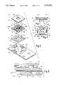
- FIG. 1is a side view of a clamp constructed in accordance with the present invention.
- FIG. 2is a bottom plan view of the clamp shown in FIG. 1.
- FIG. 3is an exploded perspective view of structure constructed in accordance with the present invention.
- FIG. 4is a side elevational view of the exploded structure illustrated in FIG. 3 incorporating a slightly different clamp and further including a heat staking iron.
- FIG. 5is an enlarged view taken along lines 5--5 in FIG. 4.
- FIG. 6is a view similar to FIG. 4 after the clamp is heat staked to the PC board.
- FIG. 7is a slightly reduced view taken along line 7--7 in FIG. 4.
- FIG. 8is a view taken along line 8--8 in FIG. 5.
- FIG. 9is an enlarged plan view of a portion of the structure illustrated in FIG. 8.
- FIG. 10is a view taken along line 10--10 in FIG. 9.
- FIG. 11is a view of a portion of a second embodiment of apparatus constructed in accordance with the present invention which is similar to the view of FIG. 5.
- FIG. 12is an enlarged view of a portion of a third embodiment of apparatus constructed in accordance with the present invention which is similar to the view of FIG. 7.
- FIG. 13is a view taken along line 13--13 in FIG. 12.
- FIG. 14is an enlarged view of a portion of a fourth embodiment of apparatus constructed in accordance with the present invention which is similar to the view of FIG. 12.
- FIG. 15is a view taken along line 15--15 in FIG. 14.
- FIG. 3indicated generally at 10 is apparatus constructed in accordance with the present invention. Included therein is a clamp 12 and a tape-assisted bonding (TAB) segment 14. Clamp 12 is also referred to herein as compressing or urging means.
- the TAB segmentincludes an integrated circuit chip or die 16 and a plurality of conductive leads, indicated generally at 18, which extend from each side of the die and which make electrical connections with the circuit formed in the die. Leads 18 are formed on a film segment 20 utilizing a conventional process. Likewise, the method for connecting leads 18 to their associated electrical contacts on the die is known.
- a z-axis conductorincludes a film or sheet 22 of nonconductive material.
- sheet 22is formed from flexible, transparent polymeric material, namely a polyimide material in the preferred embodiment.
- the sheetincludes a plurality of conductive elements, indicated generally at 24, mounted thereon so that each element protrudes from both sides of sheet 22.
- the term "z-axis"refers to conduction in the vertical direction, as viewed in FIG. 3, rather than in the horizontal direction.
- a printed circuit (PC) board 26includes a plurality of conductive leads 28 formed on the board using a conventional process. Although a printed circuit board is shown herein and referred to in the claims, it should be appreciated that any electrical substrate, such as hybrid substrates, molded circuits, flexible circuits, etc., can be utilized in practicing the present invention.
- FIG. 3A brief general description of the manner in which the preferred embodiment illustrated in FIG. 3 functions to connect leads 18 on TAB segment 14 to leads 28 on PC board 26 follows. First, clamp 12, TAB segment 14, z-axis conductor 21 and PC board 26 are aligned as shown in FIG. 3. Thereafter, the clamp is urged toward the PC board until the structure assumes the configuration shown in FIG. 4. Finally, the clamp is secured to the PC board, in a manner which is hereinafter described, so that the structure assumes the configuration illustrated in FIG. 6. Clamp 12 urges the leads on TAB segment 14 against that portion of the conductors which extend upwardly from z-axis conductor 21. The conductors which extend downwardly from the z-axis conductor are urged against the outer most portions of leads 28 on PC board 26 thus providing continuous electrical contact between leads 18 on TAB segment 14 and corresponding opposing leads on PC board 26.
- Clamp 12includes a substantially planar top portion 30.
- posts 32, 34, 36, 38such being also referred to herein as elongate means, extend downwardly from the lower side of top portion 30.
- the postsare substantially the same length and are spaced as shown in FIG. 2.
- Posts 32-38 and top portion 30comprise molded polycarbonate. Any other relatively hard plastic such as acrylic or vinyl is also suitable.
- compression members 40, 42, 44, 46also extend downwardly from the lower side of top portion 30.
- the compression memberseach include a downwardly directed surface 48, 50, 52, 54.
- Clamp 12is constructed utilizing a conventional two step molding process.
- Surfaces 48-54are substantially planar and are referred to herein as a clamping surface or as a resilient portion of clamp 12. As will be seen hereinafter, surfaces 48-54 compress TAB segment 14 and z-axis conductor 21 against PC board 26 thereby maintaining low contact resistance, via conductive elements 24 in z-axis conductor 21, between leads 18 on TAB segment 14 and leads 28 on PC board 26.
- FIGS. 1 and 3An opening 56 is centered on top portion 30 and is sized and positioned so that the center thereof is coaxial with the center of die 16 when the clamp is assembled to the PC board as illustrated in FIG. 6.
- the clamp of FIGS. 1 and 3is slightly different from the clamp of FIGS. 4 and 6 in that the clamp of FIGS. 4 and 6 does not include compression members 40-46.
- the clamp of FIGS. 1 and 3is preferred; however, as will later be explained, the clamp of FIGS. 4 and 6 is also usable to practice the present invention.
- Sheet 22likewise includes four holes, one of which is hole 66. Each of the holes, like hole 66, in z-axis conductor 21 are also spaced so that posts 32-38 are receivable therethrough.
- a square opening 68is substantially centered on sheet 22. The center of opening 68 is coaxial with the center of opening 64. Opening 68 is slightly larger than opening 64.
- FIG. 8An enlarged plan view of a portion of conductive elements 24 is shown in FIG. 8.
- Each of the conductive elements, like elements 70, 72, 74is substantially tubular in shape.
- Sheet 22is formed around the elements so as to form a substantially rectangular track, viewable on one side of sheet 22 in FIG. 3 and on the other side thereof in FIG. 7.
- the elements, like elements 70-74are formed in the sheet in a known manner.
- the elementsform a plurality of rows of six each with the rows arranged to form a rectangular pattern adjacent the borders of sheet 22.
- leads 28each terminate in a pad, like pads 76, 78, 80 formed on PC board 26.
- each pad, like pads 76-80 on PC board 26is beneath a corresponding pad, like pads 60, 61, 63, on TAB segment 14.
- the opposed corresponding padsare designed to make an electrical connection with one another in accordance with a pre-designed circuit which includes TAB segment 14 as well as other components (not shown) on PC board 26 which are connected to the TAB segment via leads 28 on the PC board.
- the PC boardincludes four holes, one of which is hole 81, which are aligned with corresponding holes, like holes 62 and 66 in TAB segment 14 and z-axis conductor 21, respectively.
- One of the conventional steps in the manufacturing process for creating the previously-described tape upon which the TAB segments, like TAB segment 14, are formedincludes encapsulating each die.
- commercially available encapsulantis applied to die 16 and to film 20 adjacent opening 64 from the lower side of the film.
- the encapsulanthardens thus providing a substantially rigid mechanical connection between the die and the film thereby preventing lead breakage.
- Encapsulantis similarly applied to each of the other TAB segments on the tape (not shown).
- individual z-axis conductor sheetsare positioned on a selected TAB segment, which is one of a plurality of such segments formed on the continuous tape, prior to application of the encapsulant.
- a selected TAB segmentwhich is one of a plurality of such segments formed on the continuous tape.
- encapsulantis applied to die 16 and film 20, it is also applied to film 22 adjacent opening 68.
- a z-axis conductor sheet, like sheet 21is applied to each TAB segment on the tape.
- the encapsulantis pre-cured in a conventional manner, rolled onto a reel and thereafter cured. The reel is thereafter provided to the PC board assembler who cuts the tape into individual tab segments, like tab segment 14 in FIG. 7, each having an associated z-axis conductor, like z-axis conductor 21 bonded thereto.
- the pads, like pads 60, 61, 63are generally aligned above corresponding pads, like pads 76, 78, 80, on PC board 26.
- the pads, like pads 60-63, which are formed in the terminal ends of leads 18,are preferably substantially the same width as the pads, like pads 76-80, formed on PC board 26.
- the pad widthwhich is viewable in FIG. 5, is approximately 10 mils for both pads on the TAB segment and for those on the PC board.
- the pitch, i.e., spacing, between the conductive elements, like elements 70-74, in sheet 21is approximately 3 mils.
- the generally opposing padscan be misaligned laterally with one another by more than plus or minus 5 mils. Even so, at least some of the conductive elements, like conductive elements 70-74, have an upper surface pressed against the lower surface of pad 61 and a lower surface pressed against the upper surface of pad 78 thereby making electrical connection between the opposing pads.
- the TAB segmentsare mounted on PC boards in an automated assembly line, such alignment tolerances are easily obtainable utilizing optical reflectance equipment thus obviating the need for the more expensive vision equipment which incorporates video cameras and associated signal processing equipment.
- a heat staking iron 82includes four concave portions formed on an upper surface thereof, two of which are concave portions 84, 86, opposite posts 32-38. Each of the concave portions is opposite a corresponding post.
- conventional automated machinerylowers the assembly (made up of clamp 12, TAB segment 14, z-axis conductor 21 and PC board 26) and applies pressure to the upper surface of clamp 12 thereby melting the lower ends of posts 32-38 into the concave portions, like portions 84, 86 on iron 82.
- the ironmelts the post ends and shapes the melted plastic into semispherical heads, like heads 88, 90 which secure the assembly together and maintain appropriate pressure for making low resistance contact, via the conductive elements, between opposing pads on the TAB segment and PC board.
- FIG. 11indicated generally therein is a portion of a second embodiment of the invention incorporating a modified z-axis conductor. Identifying numerals previously used herein identify corresponding structure in FIG. 11.
- z-axis conductor 21includes sheet 22, but rather than tubular elements, like tubular element 70, 72, 74, in FIG. 5, sheet 22 includes therein a plurality of spherical members 90, 92, 94.
- Sheet 22is formed around the spherical members as shown thereby causing each spherical member to present both an upwardly and downwardly directed portion.
- the spherical membersare embedded in sheet 22 to form a pattern, like the pattern of conductive elements 24 in FIG. 7.
- the spherical membersprovide essentially point contact forces when TAB segment 14 is urged downwardly thereby sandwiching the z-axis conductor between pads 60-63 and pads 76-80 in FIG. 5.
- the point contact forcesprovide good electrical contact by "scrubbing" action which results from the point contact made by the spherical members against each opposing pad.
- FIG. 12is an enlarged view of a portion of a third embodiment of apparatus constructed in accordance with the present invention.
- sheet 22which contained the tubular elements in the embodiment of FIGS. 1-10, is not utilized.
- the tubular elements, like elements 70, 72, 74 in the embodiment of FIG. 12,are formed in film segment 20 thus eliminating the need for a separate sheet, like sheet 22, disposed between TAB segment 14 and PC board 26.
- the tubular elementsform a rectangular pattern, like conductive elements 24 in FIG. 7.
- the embodiment of FIG. 12is formed by a conventional electroplating and etching process which can be readily implemented by a person having ordinary skill in the art.
- FIG. 14illustrated therein is an enlarged view of a portion of a fourth embodiment of the present invention.
- the need for a sheet, like sheet 20is eliminated because the conductive elements, like conductive elements 24 in FIG. 7, are formed on the TAB leads, like leads 61, 63.
- conductive elements 96, 98, 100are three of a plurality of such elements formed on TAB lead 61.
- Each of the other TAB leads, including TAB lead 63,includes such conductive elements formed thereon.
- the conductive elements in the embodiment of FIG. 14are referred to herein as dimples. The dimples are formed by pressing each TAB lead into a press having a preformed dimpled surface thereon which forms the dimples as shown in FIGS. 14 and 15.
- FIGS. 14 and 15is mounted on PC board 26 in the same fashion as the embodiment of FIGS. 12 and 13.
- the dimplesprovide essentially point contact forces which provide scrubbing action, as described in connection with the embodiment of FIG. 11, thereby providing enhanced electrical contact between the TAB leads and the PC board leads.
Landscapes
- Engineering & Computer Science (AREA)
- Metallurgy (AREA)
- Manufacturing & Machinery (AREA)
- Microelectronics & Electronic Packaging (AREA)
- Wire Bonding (AREA)
- Connecting Device With Holders (AREA)
- Electric Connection Of Electric Components To Printed Circuits (AREA)
Abstract
Description
Claims (25)
Priority Applications (2)
| Application Number | Priority Date | Filing Date | Title |
|---|---|---|---|
| US07/529,069US5046953A (en) | 1990-05-25 | 1990-05-25 | Method and apparatus for mounting an integrated circuit on a printed circuit board |
| JP14783691AJP3337480B2 (en) | 1990-05-25 | 1991-05-23 | Electrical connection part forming device |
Applications Claiming Priority (1)
| Application Number | Priority Date | Filing Date | Title |
|---|---|---|---|
| US07/529,069US5046953A (en) | 1990-05-25 | 1990-05-25 | Method and apparatus for mounting an integrated circuit on a printed circuit board |
Publications (1)
| Publication Number | Publication Date |
|---|---|
| US5046953Atrue US5046953A (en) | 1991-09-10 |
Family
ID=24108395
Family Applications (1)
| Application Number | Title | Priority Date | Filing Date |
|---|---|---|---|
| US07/529,069Expired - LifetimeUS5046953A (en) | 1990-05-25 | 1990-05-25 | Method and apparatus for mounting an integrated circuit on a printed circuit board |
Country Status (2)
| Country | Link |
|---|---|
| US (1) | US5046953A (en) |
| JP (1) | JP3337480B2 (en) |
Cited By (45)
| Publication number | Priority date | Publication date | Assignee | Title |
|---|---|---|---|---|
| US5155905A (en)* | 1991-05-03 | 1992-10-20 | Ltv Aerospace And Defense Company | Method and apparatus for attaching a circuit component to a printed circuit board |
| US5162613A (en)* | 1991-07-01 | 1992-11-10 | At&T Bell Laboratories | Integrated circuit interconnection technique |
| WO1993007659A1 (en)* | 1991-10-09 | 1993-04-15 | Ifax Corporation | Direct integrated circuit interconnection system |
| US5298686A (en)* | 1990-10-23 | 1994-03-29 | Westinghouse Electric Corp. | System and method for implementing wiring changes in a solderless printed wiring board module |
| EP0538007A3 (en)* | 1991-10-15 | 1994-07-13 | Hewlett Packard Co | Integrated circuit demountable tab apparatus |
| US5354205A (en)* | 1991-08-26 | 1994-10-11 | Hughes Aircraft Company | Electrical connections with shaped contacts |
| US5363038A (en)* | 1992-08-12 | 1994-11-08 | Fujitsu Limited | Method and apparatus for testing an unpopulated chip carrier using a module test card |
| US5368802A (en)* | 1993-05-13 | 1994-11-29 | Itt Corporation | Heat stake press and aligner and method of use |
| US5406211A (en)* | 1992-10-30 | 1995-04-11 | Japan Synthetic Rubber Co., Ltd. | Jigs for burn-in test |
| US5417577A (en)* | 1992-09-23 | 1995-05-23 | At&T Corp. | Interconnection method and apparatus |
| US5421079A (en)* | 1992-02-14 | 1995-06-06 | International Business Machines Corporation | High density, high performance memory circuit package |
| US5454160A (en)* | 1993-12-03 | 1995-10-03 | Ncr Corporation | Apparatus and method for stacking integrated circuit devices |
| EP0675569A1 (en)* | 1994-03-23 | 1995-10-04 | International Business Machines Corporation | Circuitized structure including flexible circuit with elastomeric member bonded thereto and method of making |
| US5473119A (en)* | 1993-02-05 | 1995-12-05 | W. L. Gore & Associates, Inc. | Stress-resistant circuit board |
| US5507651A (en)* | 1991-04-22 | 1996-04-16 | Kel Corporation | Connector assembly for film circuitry |
| US5600881A (en)* | 1993-05-13 | 1997-02-11 | Itt Corporation | Connector seating press |
| US5615824A (en)* | 1994-06-07 | 1997-04-01 | Tessera, Inc. | Soldering with resilient contacts |
| US5632631A (en)* | 1994-06-07 | 1997-05-27 | Tessera, Inc. | Microelectronic contacts with asperities and methods of making same |
| US5647750A (en)* | 1995-11-30 | 1997-07-15 | The Whitaker Corporation | Socket for a tape carrier package |
| US5802699A (en)* | 1994-06-07 | 1998-09-08 | Tessera, Inc. | Methods of assembling microelectronic assembly with socket for engaging bump leads |
| US5983492A (en)* | 1996-11-27 | 1999-11-16 | Tessera, Inc. | Low profile socket for microelectronic components and method for making the same |
| US6093894A (en)* | 1997-05-06 | 2000-07-25 | International Business Machines Corporation | Multiconductor bonded connection assembly with direct thermal compression bonding through a base layer |
| US6121679A (en)* | 1998-03-10 | 2000-09-19 | Luvara; John J. | Structure for printed circuit design |
| US6138892A (en)* | 1997-03-13 | 2000-10-31 | Samsung Electronics Co., Ltd. | Method for mounting an integrated circuit from a tape carrier package on a printed circuit board |
| US6191367B1 (en)* | 1995-03-03 | 2001-02-20 | Mitsubishi Denki Kabushiki Kaisha | Wiring construction body with conductive lines in a resin binder |
| US6196871B1 (en)* | 1999-02-02 | 2001-03-06 | Hon Hai Precision Ind. Co., Ltd. | Method for adjusting differential thermal expansion between an electrical socket and a circuit board |
| US6310303B1 (en) | 1998-03-10 | 2001-10-30 | John J. Luvara | Structure for printed circuit design |
| US6330996B1 (en)* | 1999-05-10 | 2001-12-18 | Asustek Computer, Inc. | Mounting fixture for CPU of a portable-type computer system |
| US6435883B1 (en)* | 1997-09-24 | 2002-08-20 | Raytheon Company | High density multichip interconnect decal grid array with epoxy interconnects and transfer tape underfill |
| US20020195695A1 (en)* | 2001-05-30 | 2002-12-26 | Miyoshi Togawa | Substrate for semiconductor device, manufacturing method thereof, semiconductor device, and frame main body |
| US20030216068A1 (en)* | 2002-05-15 | 2003-11-20 | Weiss Roger E. | Optically transparent elastomeric interconnects and method of using same |
| US6694609B2 (en) | 2001-03-22 | 2004-02-24 | Molex Incorporated | Method of making stitched LGA connector |
| US20040068868A1 (en)* | 2002-07-29 | 2004-04-15 | Atsushi Nishio | Method of mounting camera module on wiring board |
| US6722896B2 (en) | 2001-03-22 | 2004-04-20 | Molex Incorporated | Stitched LGA connector |
| US6744120B1 (en)* | 1999-03-11 | 2004-06-01 | Seiko Epson Corporation | Flexible interconnect substrate of a tape-shaped semiconductor device, semiconductor device and circuit board |
| US6752634B2 (en)* | 2001-09-21 | 2004-06-22 | Intel Corporation | Contact array for semiconductor package |
| US20040212544A1 (en)* | 1999-03-24 | 2004-10-28 | Pennaz Thomas J. | Circuit chip connector and method of connecting a circuit chip |
| US20060027937A1 (en)* | 2004-08-06 | 2006-02-09 | Brad Benson | Electrical contact encapsulation |
| US20060254051A1 (en)* | 2003-07-05 | 2006-11-16 | Daimlerchrysler Ag | Method for the space-saving installation of electrical wiring |
| US20060286827A1 (en)* | 2005-06-03 | 2006-12-21 | Kuang-Chin Lai | Land grid array integrated circuit connector |
| US20070026710A1 (en)* | 2003-09-30 | 2007-02-01 | Shuichi Inoue | Electrical connection component |
| US20070107930A1 (en)* | 2005-11-15 | 2007-05-17 | Sharp Kabushiki Kaisha | Printed circuit board and method for manufacturing the same |
| US20090311890A1 (en)* | 2006-04-28 | 2009-12-17 | Nhk Spring Co., Ltd. | Conductive Contact Holder |
| CN106961800A (en)* | 2017-03-21 | 2017-07-18 | 奥士康精密电路(惠州)有限公司 | Double IC clamps preparation method on a kind of PCB |
| DE102009044714B4 (en)* | 2008-12-09 | 2017-09-21 | Infineon Technologies Ag | Semiconductor device, semiconductor module and method for mounting the semiconductor device and for handling the semiconductor module |
Citations (13)
| Publication number | Priority date | Publication date | Assignee | Title |
|---|---|---|---|---|
| US3541222A (en)* | 1969-01-13 | 1970-11-17 | Bunker Ramo | Connector screen for interconnecting adjacent surfaces of laminar circuits and method of making |
| US3983458A (en)* | 1971-07-21 | 1976-09-28 | Corning Glass Works | Electrical device assembly and method |
| US4095867A (en)* | 1974-10-10 | 1978-06-20 | Bunker Ramo Corporation | Component connection system |
| US4144648A (en)* | 1976-07-07 | 1979-03-20 | Minnesota Mining And Manufacturing Company | Connector |
| US4371912A (en)* | 1980-10-01 | 1983-02-01 | Motorola, Inc. | Method of mounting interrelated components |
| US4381131A (en)* | 1981-05-04 | 1983-04-26 | Burroughs Corporation | Levered system connector for an integrated circuit package |
| US4390220A (en)* | 1981-04-02 | 1983-06-28 | Burroughs Corporation | Electrical connector assembly for an integrated circuit package |
| US4395084A (en)* | 1981-07-06 | 1983-07-26 | Teledyne Industries, Inc. | Electrical socket for leadless integrated circuit packages |
| US4423435A (en)* | 1980-10-27 | 1983-12-27 | Texas Instruments Incorporated | Assembly of an electronic device on an insulative substrate |
| US4553192A (en)* | 1983-08-25 | 1985-11-12 | International Business Machines Corporation | High density planar interconnected integrated circuit package |
| US4614387A (en)* | 1981-12-04 | 1986-09-30 | International Standard Electric Corporation | Connecting element for chip carriers |
| US4716049A (en)* | 1985-12-20 | 1987-12-29 | Hughes Aircraft Company | Compressive pedestal for microminiature connections |
| US4736277A (en)* | 1986-01-03 | 1988-04-05 | Motorola, Inc. | Metal printed circuit panels including mesas for coupling circuitry thereon to signal ground |
- 1990
- 1990-05-25USUS07/529,069patent/US5046953A/ennot_activeExpired - Lifetime
- 1991
- 1991-05-23JPJP14783691Apatent/JP3337480B2/ennot_activeExpired - Lifetime
Patent Citations (13)
| Publication number | Priority date | Publication date | Assignee | Title |
|---|---|---|---|---|
| US3541222A (en)* | 1969-01-13 | 1970-11-17 | Bunker Ramo | Connector screen for interconnecting adjacent surfaces of laminar circuits and method of making |
| US3983458A (en)* | 1971-07-21 | 1976-09-28 | Corning Glass Works | Electrical device assembly and method |
| US4095867A (en)* | 1974-10-10 | 1978-06-20 | Bunker Ramo Corporation | Component connection system |
| US4144648A (en)* | 1976-07-07 | 1979-03-20 | Minnesota Mining And Manufacturing Company | Connector |
| US4371912A (en)* | 1980-10-01 | 1983-02-01 | Motorola, Inc. | Method of mounting interrelated components |
| US4423435A (en)* | 1980-10-27 | 1983-12-27 | Texas Instruments Incorporated | Assembly of an electronic device on an insulative substrate |
| US4390220A (en)* | 1981-04-02 | 1983-06-28 | Burroughs Corporation | Electrical connector assembly for an integrated circuit package |
| US4381131A (en)* | 1981-05-04 | 1983-04-26 | Burroughs Corporation | Levered system connector for an integrated circuit package |
| US4395084A (en)* | 1981-07-06 | 1983-07-26 | Teledyne Industries, Inc. | Electrical socket for leadless integrated circuit packages |
| US4614387A (en)* | 1981-12-04 | 1986-09-30 | International Standard Electric Corporation | Connecting element for chip carriers |
| US4553192A (en)* | 1983-08-25 | 1985-11-12 | International Business Machines Corporation | High density planar interconnected integrated circuit package |
| US4716049A (en)* | 1985-12-20 | 1987-12-29 | Hughes Aircraft Company | Compressive pedestal for microminiature connections |
| US4736277A (en)* | 1986-01-03 | 1988-04-05 | Motorola, Inc. | Metal printed circuit panels including mesas for coupling circuitry thereon to signal ground |
Non-Patent Citations (1)
| Title |
|---|
| Raychem Development Product: A Universal IC Connector (and description of same) (1 page).* |
Cited By (64)
| Publication number | Priority date | Publication date | Assignee | Title |
|---|---|---|---|---|
| US5298686A (en)* | 1990-10-23 | 1994-03-29 | Westinghouse Electric Corp. | System and method for implementing wiring changes in a solderless printed wiring board module |
| US5507651A (en)* | 1991-04-22 | 1996-04-16 | Kel Corporation | Connector assembly for film circuitry |
| US5155905A (en)* | 1991-05-03 | 1992-10-20 | Ltv Aerospace And Defense Company | Method and apparatus for attaching a circuit component to a printed circuit board |
| US5162613A (en)* | 1991-07-01 | 1992-11-10 | At&T Bell Laboratories | Integrated circuit interconnection technique |
| US5354205A (en)* | 1991-08-26 | 1994-10-11 | Hughes Aircraft Company | Electrical connections with shaped contacts |
| WO1993007659A1 (en)* | 1991-10-09 | 1993-04-15 | Ifax Corporation | Direct integrated circuit interconnection system |
| US5435734A (en)* | 1991-10-09 | 1995-07-25 | Chow; Vincent | Direct integrated circuit interconnector system |
| EP0538007A3 (en)* | 1991-10-15 | 1994-07-13 | Hewlett Packard Co | Integrated circuit demountable tab apparatus |
| US5421079A (en)* | 1992-02-14 | 1995-06-06 | International Business Machines Corporation | High density, high performance memory circuit package |
| US5363038A (en)* | 1992-08-12 | 1994-11-08 | Fujitsu Limited | Method and apparatus for testing an unpopulated chip carrier using a module test card |
| US5417577A (en)* | 1992-09-23 | 1995-05-23 | At&T Corp. | Interconnection method and apparatus |
| US5406211A (en)* | 1992-10-30 | 1995-04-11 | Japan Synthetic Rubber Co., Ltd. | Jigs for burn-in test |
| US5473119A (en)* | 1993-02-05 | 1995-12-05 | W. L. Gore & Associates, Inc. | Stress-resistant circuit board |
| US5368802A (en)* | 1993-05-13 | 1994-11-29 | Itt Corporation | Heat stake press and aligner and method of use |
| US5600881A (en)* | 1993-05-13 | 1997-02-11 | Itt Corporation | Connector seating press |
| US5454160A (en)* | 1993-12-03 | 1995-10-03 | Ncr Corporation | Apparatus and method for stacking integrated circuit devices |
| US5932047A (en)* | 1994-03-23 | 1999-08-03 | International Business Machines Corporation | Circuitized structure including flexible circuit with elastomeric member bonded thereto and method of making |
| US5703331A (en)* | 1994-03-23 | 1997-12-30 | International Business Machines Corporation | Circuitized structure including flexible circuit with elastomeric member bonded thereto |
| EP0675569A1 (en)* | 1994-03-23 | 1995-10-04 | International Business Machines Corporation | Circuitized structure including flexible circuit with elastomeric member bonded thereto and method of making |
| US5615824A (en)* | 1994-06-07 | 1997-04-01 | Tessera, Inc. | Soldering with resilient contacts |
| US5632631A (en)* | 1994-06-07 | 1997-05-27 | Tessera, Inc. | Microelectronic contacts with asperities and methods of making same |
| US5802699A (en)* | 1994-06-07 | 1998-09-08 | Tessera, Inc. | Methods of assembling microelectronic assembly with socket for engaging bump leads |
| US5812378A (en)* | 1994-06-07 | 1998-09-22 | Tessera, Inc. | Microelectronic connector for engaging bump leads |
| US5934914A (en)* | 1994-06-07 | 1999-08-10 | Tessera, Inc. | Microelectronic contacts with asperities and methods of making same |
| US5980270A (en)* | 1994-06-07 | 1999-11-09 | Tessera, Inc. | Soldering with resilient contacts |
| US6938338B2 (en) | 1994-06-07 | 2005-09-06 | Tessera, Inc. | Method of making an electronic contact |
| US6205660B1 (en) | 1994-06-07 | 2001-03-27 | Tessera, Inc. | Method of making an electronic contact |
| US6191367B1 (en)* | 1995-03-03 | 2001-02-20 | Mitsubishi Denki Kabushiki Kaisha | Wiring construction body with conductive lines in a resin binder |
| US5647750A (en)* | 1995-11-30 | 1997-07-15 | The Whitaker Corporation | Socket for a tape carrier package |
| US6229100B1 (en) | 1996-11-27 | 2001-05-08 | Tessera, Inc. | Low profile socket for microelectronic components and method for making the same |
| US5983492A (en)* | 1996-11-27 | 1999-11-16 | Tessera, Inc. | Low profile socket for microelectronic components and method for making the same |
| US6138892A (en)* | 1997-03-13 | 2000-10-31 | Samsung Electronics Co., Ltd. | Method for mounting an integrated circuit from a tape carrier package on a printed circuit board |
| US6446335B1 (en) | 1997-05-06 | 2002-09-10 | International Business Machines Corporation | Direct thermal compression bonding through a multiconductor base layer |
| US6093894A (en)* | 1997-05-06 | 2000-07-25 | International Business Machines Corporation | Multiconductor bonded connection assembly with direct thermal compression bonding through a base layer |
| US6435883B1 (en)* | 1997-09-24 | 2002-08-20 | Raytheon Company | High density multichip interconnect decal grid array with epoxy interconnects and transfer tape underfill |
| US6310303B1 (en) | 1998-03-10 | 2001-10-30 | John J. Luvara | Structure for printed circuit design |
| US6121679A (en)* | 1998-03-10 | 2000-09-19 | Luvara; John J. | Structure for printed circuit design |
| US6196871B1 (en)* | 1999-02-02 | 2001-03-06 | Hon Hai Precision Ind. Co., Ltd. | Method for adjusting differential thermal expansion between an electrical socket and a circuit board |
| US6744120B1 (en)* | 1999-03-11 | 2004-06-01 | Seiko Epson Corporation | Flexible interconnect substrate of a tape-shaped semiconductor device, semiconductor device and circuit board |
| US6891110B1 (en)* | 1999-03-24 | 2005-05-10 | Motorola, Inc. | Circuit chip connector and method of connecting a circuit chip |
| US7300863B2 (en) | 1999-03-24 | 2007-11-27 | Motorola, Inc. | Circuit chip connector and method of connecting a circuit chip |
| US20040212544A1 (en)* | 1999-03-24 | 2004-10-28 | Pennaz Thomas J. | Circuit chip connector and method of connecting a circuit chip |
| US6330996B1 (en)* | 1999-05-10 | 2001-12-18 | Asustek Computer, Inc. | Mounting fixture for CPU of a portable-type computer system |
| US6722896B2 (en) | 2001-03-22 | 2004-04-20 | Molex Incorporated | Stitched LGA connector |
| US6694609B2 (en) | 2001-03-22 | 2004-02-24 | Molex Incorporated | Method of making stitched LGA connector |
| US7129578B2 (en)* | 2001-05-30 | 2006-10-31 | Sony Corporation | Substrate for semiconductor device, manufacturing method thereof, semiconductor device, and frame main body |
| US20020195695A1 (en)* | 2001-05-30 | 2002-12-26 | Miyoshi Togawa | Substrate for semiconductor device, manufacturing method thereof, semiconductor device, and frame main body |
| US6752634B2 (en)* | 2001-09-21 | 2004-06-22 | Intel Corporation | Contact array for semiconductor package |
| US20030216068A1 (en)* | 2002-05-15 | 2003-11-20 | Weiss Roger E. | Optically transparent elastomeric interconnects and method of using same |
| US6862804B2 (en)* | 2002-07-29 | 2005-03-08 | Mitsumi Electric Co., Ltd. | Method of mounting camera module on wiring board |
| US20040068868A1 (en)* | 2002-07-29 | 2004-04-15 | Atsushi Nishio | Method of mounting camera module on wiring board |
| US20060254051A1 (en)* | 2003-07-05 | 2006-11-16 | Daimlerchrysler Ag | Method for the space-saving installation of electrical wiring |
| US7419387B2 (en)* | 2003-09-30 | 2008-09-02 | J.S.T. Mfg. Co., Ltd. | Electric connection member utilizing ansiotropically conductive sheets |
| US20070026710A1 (en)* | 2003-09-30 | 2007-02-01 | Shuichi Inoue | Electrical connection component |
| US20060027937A1 (en)* | 2004-08-06 | 2006-02-09 | Brad Benson | Electrical contact encapsulation |
| US7475964B2 (en) | 2004-08-06 | 2009-01-13 | Hewlett-Packard Development Company, L.P. | Electrical contact encapsulation |
| US20060286827A1 (en)* | 2005-06-03 | 2006-12-21 | Kuang-Chin Lai | Land grid array integrated circuit connector |
| US20070107930A1 (en)* | 2005-11-15 | 2007-05-17 | Sharp Kabushiki Kaisha | Printed circuit board and method for manufacturing the same |
| US7807932B2 (en)* | 2005-11-15 | 2010-10-05 | Sharp Kabushiki Kaisha | Printed circuit board and method for manufacturing the same |
| US20090311890A1 (en)* | 2006-04-28 | 2009-12-17 | Nhk Spring Co., Ltd. | Conductive Contact Holder |
| US7845955B2 (en)* | 2006-04-28 | 2010-12-07 | Nhk Spring Co., Ltd. | Conductive contact holder |
| DE102009044714B4 (en)* | 2008-12-09 | 2017-09-21 | Infineon Technologies Ag | Semiconductor device, semiconductor module and method for mounting the semiconductor device and for handling the semiconductor module |
| CN106961800A (en)* | 2017-03-21 | 2017-07-18 | 奥士康精密电路(惠州)有限公司 | Double IC clamps preparation method on a kind of PCB |
| CN106961800B (en)* | 2017-03-21 | 2019-03-29 | 奥士康精密电路(惠州)有限公司 | Double IC clamp production method on a kind of PCB |
Also Published As
| Publication number | Publication date |
|---|---|
| JPH04229692A (en) | 1992-08-19 |
| JP3337480B2 (en) | 2002-10-21 |
Similar Documents
| Publication | Publication Date | Title |
|---|---|---|
| US5046953A (en) | Method and apparatus for mounting an integrated circuit on a printed circuit board | |
| US5041015A (en) | Electrical jumper assembly | |
| US5255430A (en) | Method of assembling a module for a smart card | |
| KR940006185Y1 (en) | IC module | |
| EP0558325B1 (en) | Raised feature on substrate for flip chip interconnection | |
| US5717252A (en) | Solder-ball connected semiconductor device with a recessed chip mounting area | |
| US4815981A (en) | Flexible printed circuit board terminal structure | |
| US4414741A (en) | Process for interconnecting components on a PCB | |
| JPH0513913A (en) | Flexible cable connecting device for circuit substrate | |
| US6037662A (en) | Chip scale package | |
| US5501612A (en) | Low profile board-to-board electrical connector | |
| US4766426A (en) | Display panel assembly having a plurality of film carrier tapes on each of which a semiconductor divice is mounted | |
| US4835859A (en) | Method of forming a contact bump | |
| JP3217876B2 (en) | Mold for manufacturing semiconductor electronic device structure and method of manufacturing semiconductor electronic device structure using the same | |
| US4687266A (en) | Electrical connecting terminal | |
| US4223435A (en) | Circuit board with self-locking terminals | |
| US4691188A (en) | Circuit board | |
| JPH0936155A (en) | Manufacture of semiconductor device | |
| JPS6330793B2 (en) | ||
| JP3848577B2 (en) | Flexible wiring board | |
| JPH0618909A (en) | Flexible circuit board with electric conductive anisotropic film | |
| JP2553615B2 (en) | Film carrier | |
| JPS6348144Y2 (en) | ||
| JPH033972Y2 (en) | ||
| JP2773707B2 (en) | Manufacturing method of hybrid integrated circuit device |
Legal Events
| Date | Code | Title | Description |
|---|---|---|---|
| AS | Assignment | Owner name:HEWLETT-PACKARD COMPANY, PALO ALTO, CA A CORP. OF Free format text:ASSIGNMENT OF ASSIGNORS INTEREST.;ASSIGNOR:KEIL, RONALD W.;REEL/FRAME:005437/0949 Effective date:19900522 Owner name:HEWLETT-PACKARD COMPANY, PALO ALTO, CA A CA CORP. Free format text:ASSIGNMENT OF ASSIGNORS INTEREST.;ASSIGNORS:SHREEVE, ROBERT W.;DOBBS, MICHAEL D.;BURRIS, LUCY E.;AND OTHERS;REEL/FRAME:005437/0946;SIGNING DATES FROM 19900419 TO 19900514 | |
| STCF | Information on status: patent grant | Free format text:PATENTED CASE | |
| FEPP | Fee payment procedure | Free format text:PAYOR NUMBER ASSIGNED (ORIGINAL EVENT CODE: ASPN); ENTITY STATUS OF PATENT OWNER: LARGE ENTITY | |
| FPAY | Fee payment | Year of fee payment:4 | |
| FPAY | Fee payment | Year of fee payment:8 | |
| AS | Assignment | Owner name:HEWLETT-PACKARD COMPANY, A DELAWARE CORPORATION, C Free format text:MERGER;ASSIGNOR:HEWLETT-PACKARD COMPANY, A CALIFORNIA CORPORATION;REEL/FRAME:010841/0649 Effective date:19980520 | |
| AS | Assignment | Owner name:AGILENT TECHNOLOGIES INC., CALIFORNIA Free format text:ASSIGNMENT OF ASSIGNORS INTEREST;ASSIGNOR:HEWLETT-PACKARD COMPANY, A DELAWARE CORPORATION;REEL/FRAME:010901/0336 Effective date:20000520 | |
| FPAY | Fee payment | Year of fee payment:12 | |
| AS | Assignment | Owner name:AVAGO TECHNOLOGIES GENERAL IP PTE. LTD., SINGAPORE Free format text:ASSIGNMENT OF ASSIGNORS INTEREST;ASSIGNOR:AGILENT TECHNOLOGIES, INC.;REEL/FRAME:017207/0020 Effective date:20051201 | |
| AS | Assignment | Owner name:AVAGO TECHNOLOGIES ECBU IP (SINGAPORE) PTE. LTD., SINGAPORE Free format text:ASSIGNMENT OF ASSIGNORS INTEREST;ASSIGNOR:AVAGO TECHNOLOGIES GENERAL IP (SINGAPORE) PTE. LTD.;REEL/FRAME:017675/0518 Effective date:20060127 Owner name:AVAGO TECHNOLOGIES ECBU IP (SINGAPORE) PTE. LTD.,S Free format text:ASSIGNMENT OF ASSIGNORS INTEREST;ASSIGNOR:AVAGO TECHNOLOGIES GENERAL IP (SINGAPORE) PTE. LTD.;REEL/FRAME:017675/0518 Effective date:20060127 Owner name:AVAGO TECHNOLOGIES ECBU IP (SINGAPORE) PTE. LTD., Free format text:ASSIGNMENT OF ASSIGNORS INTEREST;ASSIGNOR:AVAGO TECHNOLOGIES GENERAL IP (SINGAPORE) PTE. LTD.;REEL/FRAME:017675/0518 Effective date:20060127 | |
| AS | Assignment | Owner name:AVAGO TECHNOLOGIES GENERAL IP (SINGAPORE) PTE. LTD Free format text:CORRECTIVE ASSIGNMENT TO CORRECT THE NAME OF THE ASSIGNEE PREVIOUSLY RECORDED ON REEL 017207 FRAME 0020. ASSIGNOR(S) HEREBY CONFIRMS THE ASSIGNMENT;ASSIGNOR:AGILENT TECHNOLOGIES, INC.;REEL/FRAME:038633/0001 Effective date:20051201 |