US5046161A - Flip chip type semiconductor device - Google Patents
Flip chip type semiconductor deviceDownload PDFInfo
- Publication number
- US5046161A US5046161AUS07/314,166US31416689AUS5046161AUS 5046161 AUS5046161 AUS 5046161AUS 31416689 AUS31416689 AUS 31416689AUS 5046161 AUS5046161 AUS 5046161A
- Authority
- US
- United States
- Prior art keywords
- semiconductor device
- type semiconductor
- flip chip
- chip type
- openings
- Prior art date
- Legal status (The legal status is an assumption and is not a legal conclusion. Google has not performed a legal analysis and makes no representation as to the accuracy of the status listed.)
- Expired - Lifetime
Links
Images


Classifications
- H—ELECTRICITY
- H01—ELECTRIC ELEMENTS
- H01L—SEMICONDUCTOR DEVICES NOT COVERED BY CLASS H10
- H01L24/00—Arrangements for connecting or disconnecting semiconductor or solid-state bodies; Methods or apparatus related thereto
- H01L24/01—Means for bonding being attached to, or being formed on, the surface to be connected, e.g. chip-to-package, die-attach, "first-level" interconnects; Manufacturing methods related thereto
- H01L24/10—Bump connectors ; Manufacturing methods related thereto
- H01L24/12—Structure, shape, material or disposition of the bump connectors prior to the connecting process
- H01L24/13—Structure, shape, material or disposition of the bump connectors prior to the connecting process of an individual bump connector
- H—ELECTRICITY
- H01—ELECTRIC ELEMENTS
- H01L—SEMICONDUCTOR DEVICES NOT COVERED BY CLASS H10
- H01L24/00—Arrangements for connecting or disconnecting semiconductor or solid-state bodies; Methods or apparatus related thereto
- H01L24/80—Methods for connecting semiconductor or other solid state bodies using means for bonding being attached to, or being formed on, the surface to be connected
- H01L24/81—Methods for connecting semiconductor or other solid state bodies using means for bonding being attached to, or being formed on, the surface to be connected using a bump connector
- H—ELECTRICITY
- H01—ELECTRIC ELEMENTS
- H01L—SEMICONDUCTOR DEVICES NOT COVERED BY CLASS H10
- H01L2224/00—Indexing scheme for arrangements for connecting or disconnecting semiconductor or solid-state bodies and methods related thereto as covered by H01L24/00
- H01L2224/01—Means for bonding being attached to, or being formed on, the surface to be connected, e.g. chip-to-package, die-attach, "first-level" interconnects; Manufacturing methods related thereto
- H01L2224/02—Bonding areas; Manufacturing methods related thereto
- H01L2224/04—Structure, shape, material or disposition of the bonding areas prior to the connecting process
- H01L2224/05—Structure, shape, material or disposition of the bonding areas prior to the connecting process of an individual bonding area
- H01L2224/05001—Internal layers
- H01L2224/05099—Material
- H01L2224/051—Material with a principal constituent of the material being a metal or a metalloid, e.g. boron [B], silicon [Si], germanium [Ge], arsenic [As], antimony [Sb], tellurium [Te] and polonium [Po], and alloys thereof
- H01L2224/05117—Material with a principal constituent of the material being a metal or a metalloid, e.g. boron [B], silicon [Si], germanium [Ge], arsenic [As], antimony [Sb], tellurium [Te] and polonium [Po], and alloys thereof the principal constituent melting at a temperature of greater than or equal to 400°C and less than 950°C
- H01L2224/05124—Aluminium [Al] as principal constituent
- H—ELECTRICITY
- H01—ELECTRIC ELEMENTS
- H01L—SEMICONDUCTOR DEVICES NOT COVERED BY CLASS H10
- H01L2224/00—Indexing scheme for arrangements for connecting or disconnecting semiconductor or solid-state bodies and methods related thereto as covered by H01L24/00
- H01L2224/01—Means for bonding being attached to, or being formed on, the surface to be connected, e.g. chip-to-package, die-attach, "first-level" interconnects; Manufacturing methods related thereto
- H01L2224/02—Bonding areas; Manufacturing methods related thereto
- H01L2224/04—Structure, shape, material or disposition of the bonding areas prior to the connecting process
- H01L2224/05—Structure, shape, material or disposition of the bonding areas prior to the connecting process of an individual bonding area
- H01L2224/05001—Internal layers
- H01L2224/05099—Material
- H01L2224/051—Material with a principal constituent of the material being a metal or a metalloid, e.g. boron [B], silicon [Si], germanium [Ge], arsenic [As], antimony [Sb], tellurium [Te] and polonium [Po], and alloys thereof
- H01L2224/05163—Material with a principal constituent of the material being a metal or a metalloid, e.g. boron [B], silicon [Si], germanium [Ge], arsenic [As], antimony [Sb], tellurium [Te] and polonium [Po], and alloys thereof the principal constituent melting at a temperature of greater than 1550°C
- H01L2224/05166—Titanium [Ti] as principal constituent
- H—ELECTRICITY
- H01—ELECTRIC ELEMENTS
- H01L—SEMICONDUCTOR DEVICES NOT COVERED BY CLASS H10
- H01L2224/00—Indexing scheme for arrangements for connecting or disconnecting semiconductor or solid-state bodies and methods related thereto as covered by H01L24/00
- H01L2224/01—Means for bonding being attached to, or being formed on, the surface to be connected, e.g. chip-to-package, die-attach, "first-level" interconnects; Manufacturing methods related thereto
- H01L2224/02—Bonding areas; Manufacturing methods related thereto
- H01L2224/04—Structure, shape, material or disposition of the bonding areas prior to the connecting process
- H01L2224/05—Structure, shape, material or disposition of the bonding areas prior to the connecting process of an individual bonding area
- H01L2224/05001—Internal layers
- H01L2224/05099—Material
- H01L2224/051—Material with a principal constituent of the material being a metal or a metalloid, e.g. boron [B], silicon [Si], germanium [Ge], arsenic [As], antimony [Sb], tellurium [Te] and polonium [Po], and alloys thereof
- H01L2224/05163—Material with a principal constituent of the material being a metal or a metalloid, e.g. boron [B], silicon [Si], germanium [Ge], arsenic [As], antimony [Sb], tellurium [Te] and polonium [Po], and alloys thereof the principal constituent melting at a temperature of greater than 1550°C
- H01L2224/05171—Chromium [Cr] as principal constituent
- H—ELECTRICITY
- H01—ELECTRIC ELEMENTS
- H01L—SEMICONDUCTOR DEVICES NOT COVERED BY CLASS H10
- H01L2224/00—Indexing scheme for arrangements for connecting or disconnecting semiconductor or solid-state bodies and methods related thereto as covered by H01L24/00
- H01L2224/01—Means for bonding being attached to, or being formed on, the surface to be connected, e.g. chip-to-package, die-attach, "first-level" interconnects; Manufacturing methods related thereto
- H01L2224/02—Bonding areas; Manufacturing methods related thereto
- H01L2224/04—Structure, shape, material or disposition of the bonding areas prior to the connecting process
- H01L2224/05—Structure, shape, material or disposition of the bonding areas prior to the connecting process of an individual bonding area
- H01L2224/0554—External layer
- H01L2224/05599—Material
- H01L2224/056—Material with a principal constituent of the material being a metal or a metalloid, e.g. boron [B], silicon [Si], germanium [Ge], arsenic [As], antimony [Sb], tellurium [Te] and polonium [Po], and alloys thereof
- H01L2224/05638—Material with a principal constituent of the material being a metal or a metalloid, e.g. boron [B], silicon [Si], germanium [Ge], arsenic [As], antimony [Sb], tellurium [Te] and polonium [Po], and alloys thereof the principal constituent melting at a temperature of greater than or equal to 950°C and less than 1550°C
- H01L2224/05647—Copper [Cu] as principal constituent
- H—ELECTRICITY
- H01—ELECTRIC ELEMENTS
- H01L—SEMICONDUCTOR DEVICES NOT COVERED BY CLASS H10
- H01L2224/00—Indexing scheme for arrangements for connecting or disconnecting semiconductor or solid-state bodies and methods related thereto as covered by H01L24/00
- H01L2224/01—Means for bonding being attached to, or being formed on, the surface to be connected, e.g. chip-to-package, die-attach, "first-level" interconnects; Manufacturing methods related thereto
- H01L2224/02—Bonding areas; Manufacturing methods related thereto
- H01L2224/04—Structure, shape, material or disposition of the bonding areas prior to the connecting process
- H01L2224/06—Structure, shape, material or disposition of the bonding areas prior to the connecting process of a plurality of bonding areas
- H01L2224/061—Disposition
- H01L2224/0612—Layout
- H01L2224/0616—Random array, i.e. array with no symmetry
- H—ELECTRICITY
- H01—ELECTRIC ELEMENTS
- H01L—SEMICONDUCTOR DEVICES NOT COVERED BY CLASS H10
- H01L2224/00—Indexing scheme for arrangements for connecting or disconnecting semiconductor or solid-state bodies and methods related thereto as covered by H01L24/00
- H01L2224/01—Means for bonding being attached to, or being formed on, the surface to be connected, e.g. chip-to-package, die-attach, "first-level" interconnects; Manufacturing methods related thereto
- H01L2224/10—Bump connectors; Manufacturing methods related thereto
- H01L2224/12—Structure, shape, material or disposition of the bump connectors prior to the connecting process
- H01L2224/13—Structure, shape, material or disposition of the bump connectors prior to the connecting process of an individual bump connector
- H01L2224/13001—Core members of the bump connector
- H01L2224/13099—Material
- H—ELECTRICITY
- H01—ELECTRIC ELEMENTS
- H01L—SEMICONDUCTOR DEVICES NOT COVERED BY CLASS H10
- H01L2224/00—Indexing scheme for arrangements for connecting or disconnecting semiconductor or solid-state bodies and methods related thereto as covered by H01L24/00
- H01L2224/01—Means for bonding being attached to, or being formed on, the surface to be connected, e.g. chip-to-package, die-attach, "first-level" interconnects; Manufacturing methods related thereto
- H01L2224/10—Bump connectors; Manufacturing methods related thereto
- H01L2224/15—Structure, shape, material or disposition of the bump connectors after the connecting process
- H01L2224/16—Structure, shape, material or disposition of the bump connectors after the connecting process of an individual bump connector
- H—ELECTRICITY
- H01—ELECTRIC ELEMENTS
- H01L—SEMICONDUCTOR DEVICES NOT COVERED BY CLASS H10
- H01L2224/00—Indexing scheme for arrangements for connecting or disconnecting semiconductor or solid-state bodies and methods related thereto as covered by H01L24/00
- H01L2224/80—Methods for connecting semiconductor or other solid state bodies using means for bonding being attached to, or being formed on, the surface to be connected
- H01L2224/81—Methods for connecting semiconductor or other solid state bodies using means for bonding being attached to, or being formed on, the surface to be connected using a bump connector
- H01L2224/818—Bonding techniques
- H01L2224/81801—Soldering or alloying
- H—ELECTRICITY
- H01—ELECTRIC ELEMENTS
- H01L—SEMICONDUCTOR DEVICES NOT COVERED BY CLASS H10
- H01L2924/00—Indexing scheme for arrangements or methods for connecting or disconnecting semiconductor or solid-state bodies as covered by H01L24/00
- H01L2924/0001—Technical content checked by a classifier
- H01L2924/00013—Fully indexed content
- H—ELECTRICITY
- H01—ELECTRIC ELEMENTS
- H01L—SEMICONDUCTOR DEVICES NOT COVERED BY CLASS H10
- H01L2924/00—Indexing scheme for arrangements or methods for connecting or disconnecting semiconductor or solid-state bodies as covered by H01L24/00
- H01L2924/01—Chemical elements
- H01L2924/01005—Boron [B]
- H—ELECTRICITY
- H01—ELECTRIC ELEMENTS
- H01L—SEMICONDUCTOR DEVICES NOT COVERED BY CLASS H10
- H01L2924/00—Indexing scheme for arrangements or methods for connecting or disconnecting semiconductor or solid-state bodies as covered by H01L24/00
- H01L2924/01—Chemical elements
- H01L2924/01006—Carbon [C]
- H—ELECTRICITY
- H01—ELECTRIC ELEMENTS
- H01L—SEMICONDUCTOR DEVICES NOT COVERED BY CLASS H10
- H01L2924/00—Indexing scheme for arrangements or methods for connecting or disconnecting semiconductor or solid-state bodies as covered by H01L24/00
- H01L2924/01—Chemical elements
- H01L2924/01013—Aluminum [Al]
- H—ELECTRICITY
- H01—ELECTRIC ELEMENTS
- H01L—SEMICONDUCTOR DEVICES NOT COVERED BY CLASS H10
- H01L2924/00—Indexing scheme for arrangements or methods for connecting or disconnecting semiconductor or solid-state bodies as covered by H01L24/00
- H01L2924/01—Chemical elements
- H01L2924/01014—Silicon [Si]
- H—ELECTRICITY
- H01—ELECTRIC ELEMENTS
- H01L—SEMICONDUCTOR DEVICES NOT COVERED BY CLASS H10
- H01L2924/00—Indexing scheme for arrangements or methods for connecting or disconnecting semiconductor or solid-state bodies as covered by H01L24/00
- H01L2924/01—Chemical elements
- H01L2924/01015—Phosphorus [P]
- H—ELECTRICITY
- H01—ELECTRIC ELEMENTS
- H01L—SEMICONDUCTOR DEVICES NOT COVERED BY CLASS H10
- H01L2924/00—Indexing scheme for arrangements or methods for connecting or disconnecting semiconductor or solid-state bodies as covered by H01L24/00
- H01L2924/01—Chemical elements
- H01L2924/01019—Potassium [K]
- H—ELECTRICITY
- H01—ELECTRIC ELEMENTS
- H01L—SEMICONDUCTOR DEVICES NOT COVERED BY CLASS H10
- H01L2924/00—Indexing scheme for arrangements or methods for connecting or disconnecting semiconductor or solid-state bodies as covered by H01L24/00
- H01L2924/01—Chemical elements
- H01L2924/01022—Titanium [Ti]
- H—ELECTRICITY
- H01—ELECTRIC ELEMENTS
- H01L—SEMICONDUCTOR DEVICES NOT COVERED BY CLASS H10
- H01L2924/00—Indexing scheme for arrangements or methods for connecting or disconnecting semiconductor or solid-state bodies as covered by H01L24/00
- H01L2924/01—Chemical elements
- H01L2924/01024—Chromium [Cr]
- H—ELECTRICITY
- H01—ELECTRIC ELEMENTS
- H01L—SEMICONDUCTOR DEVICES NOT COVERED BY CLASS H10
- H01L2924/00—Indexing scheme for arrangements or methods for connecting or disconnecting semiconductor or solid-state bodies as covered by H01L24/00
- H01L2924/01—Chemical elements
- H01L2924/01029—Copper [Cu]
- H—ELECTRICITY
- H01—ELECTRIC ELEMENTS
- H01L—SEMICONDUCTOR DEVICES NOT COVERED BY CLASS H10
- H01L2924/00—Indexing scheme for arrangements or methods for connecting or disconnecting semiconductor or solid-state bodies as covered by H01L24/00
- H01L2924/01—Chemical elements
- H01L2924/01033—Arsenic [As]
- H—ELECTRICITY
- H01—ELECTRIC ELEMENTS
- H01L—SEMICONDUCTOR DEVICES NOT COVERED BY CLASS H10
- H01L2924/00—Indexing scheme for arrangements or methods for connecting or disconnecting semiconductor or solid-state bodies as covered by H01L24/00
- H01L2924/01—Chemical elements
- H01L2924/0105—Tin [Sn]
- H—ELECTRICITY
- H01—ELECTRIC ELEMENTS
- H01L—SEMICONDUCTOR DEVICES NOT COVERED BY CLASS H10
- H01L2924/00—Indexing scheme for arrangements or methods for connecting or disconnecting semiconductor or solid-state bodies as covered by H01L24/00
- H01L2924/01—Chemical elements
- H01L2924/01078—Platinum [Pt]
- H—ELECTRICITY
- H01—ELECTRIC ELEMENTS
- H01L—SEMICONDUCTOR DEVICES NOT COVERED BY CLASS H10
- H01L2924/00—Indexing scheme for arrangements or methods for connecting or disconnecting semiconductor or solid-state bodies as covered by H01L24/00
- H01L2924/01—Chemical elements
- H01L2924/01082—Lead [Pb]
- H—ELECTRICITY
- H01—ELECTRIC ELEMENTS
- H01L—SEMICONDUCTOR DEVICES NOT COVERED BY CLASS H10
- H01L2924/00—Indexing scheme for arrangements or methods for connecting or disconnecting semiconductor or solid-state bodies as covered by H01L24/00
- H01L2924/013—Alloys
- H01L2924/0132—Binary Alloys
- H01L2924/01322—Eutectic Alloys, i.e. obtained by a liquid transforming into two solid phases
- H—ELECTRICITY
- H01—ELECTRIC ELEMENTS
- H01L—SEMICONDUCTOR DEVICES NOT COVERED BY CLASS H10
- H01L2924/00—Indexing scheme for arrangements or methods for connecting or disconnecting semiconductor or solid-state bodies as covered by H01L24/00
- H01L2924/013—Alloys
- H01L2924/014—Solder alloys
- H—ELECTRICITY
- H01—ELECTRIC ELEMENTS
- H01L—SEMICONDUCTOR DEVICES NOT COVERED BY CLASS H10
- H01L2924/00—Indexing scheme for arrangements or methods for connecting or disconnecting semiconductor or solid-state bodies as covered by H01L24/00
- H01L2924/095—Indexing scheme for arrangements or methods for connecting or disconnecting semiconductor or solid-state bodies as covered by H01L24/00 with a principal constituent of the material being a combination of two or more materials provided in the groups H01L2924/013 - H01L2924/0715
- H01L2924/097—Glass-ceramics, e.g. devitrified glass
- H01L2924/09701—Low temperature co-fired ceramic [LTCC]
- H—ELECTRICITY
- H01—ELECTRIC ELEMENTS
- H01L—SEMICONDUCTOR DEVICES NOT COVERED BY CLASS H10
- H01L2924/00—Indexing scheme for arrangements or methods for connecting or disconnecting semiconductor or solid-state bodies as covered by H01L24/00
- H01L2924/15—Details of package parts other than the semiconductor or other solid state devices to be connected
- H01L2924/151—Die mounting substrate
- H01L2924/1515—Shape
- H01L2924/15153—Shape the die mounting substrate comprising a recess for hosting the device
- H—ELECTRICITY
- H01—ELECTRIC ELEMENTS
- H01L—SEMICONDUCTOR DEVICES NOT COVERED BY CLASS H10
- H01L2924/00—Indexing scheme for arrangements or methods for connecting or disconnecting semiconductor or solid-state bodies as covered by H01L24/00
- H01L2924/15—Details of package parts other than the semiconductor or other solid state devices to be connected
- H01L2924/151—Die mounting substrate
- H01L2924/15165—Monolayer substrate
- H—ELECTRICITY
- H01—ELECTRIC ELEMENTS
- H01L—SEMICONDUCTOR DEVICES NOT COVERED BY CLASS H10
- H01L2924/00—Indexing scheme for arrangements or methods for connecting or disconnecting semiconductor or solid-state bodies as covered by H01L24/00
- H01L2924/15—Details of package parts other than the semiconductor or other solid state devices to be connected
- H01L2924/161—Cap
- H01L2924/1615—Shape
- H01L2924/16195—Flat cap [not enclosing an internal cavity]
- H—ELECTRICITY
- H01—ELECTRIC ELEMENTS
- H01L—SEMICONDUCTOR DEVICES NOT COVERED BY CLASS H10
- H01L2924/00—Indexing scheme for arrangements or methods for connecting or disconnecting semiconductor or solid-state bodies as covered by H01L24/00
- H01L2924/19—Details of hybrid assemblies other than the semiconductor or other solid state devices to be connected
- H01L2924/1901—Structure
- H01L2924/1904—Component type
- H01L2924/19043—Component type being a resistor
- H—ELECTRICITY
- H01—ELECTRIC ELEMENTS
- H01L—SEMICONDUCTOR DEVICES NOT COVERED BY CLASS H10
- H01L2924/00—Indexing scheme for arrangements or methods for connecting or disconnecting semiconductor or solid-state bodies as covered by H01L24/00
- H01L2924/19—Details of hybrid assemblies other than the semiconductor or other solid state devices to be connected
- H01L2924/191—Disposition
- H01L2924/19101—Disposition of discrete passive components
- H01L2924/19107—Disposition of discrete passive components off-chip wires
Definitions
- the present inventionrelates to a flip chip type semiconductor device, and more particularly to the device using a polyimide film on the substrate.
- a polyimide filmcan be formed on a semiconductor substrate (wafer) by a spin-coating process similarly to the photo-resist coating and has many beneficial properties, that is, high resistances to a relatively high temperature, to organic solvents, and to radiations. Therefore, the polyimide film has been widely used in semiconductor devices as a passivation film which substantially covers the substrate. Further, in flip chip type semiconductor devices, the polyimide film as the passivation film has been used for defining positions of solder bump terminals; they are formed in apertures provided in the film. The technology is described in U.K. patent 1,230,421, for example.
- a flip chip type semiconductor devicehaving a composite passivation insulating film consisting of an inorganic insulating film as a lower film and a polyimide film as an upper film, which is as shown in Laid-open Japanese Patent Application No. 53-68163, for example.
- aperturesare formed in the composite film with the same figure in the polyimide film and in the inorganic insulating film, and then solder bumps are formed in the apertures to contact electrode pads thereunder.
- the aperture commonly formed in the polyimide film and in the inorganic filmis of a rectangular plan shape
- the bottom surface of each bump consisting of a solder bump terminal or of a solder bump terminal and a barrier metal filmbecomes rectangular and it is difficult to shape the solder bump in a spherical shape with the result being the non-uniformity of the height of the solder bumps. Consequently, when the semiconductor pellet having the non-uniformity solder bumps is mounted to a substrate of a package or a print board by melting the solder bumps in the face-down bonding arrangement, such a structure induces insufficient connection and reduces the production yield and reliability.
- the common apertureis of a circular in plan, the problem can be solved.
- merits of a mass-production for fabricating semicondutor devicescannot be obtained, because for obtaining the merits, the intermediate products after finishing the process step for forming apertures in the inorganic insulating film must be adapted to usual bonding wire type semiconductor devices as well as to the flip chip type semiconductor devices.
- the bonding wire type semiconductor devicesnecessitate the apertures to be rectangular plan shape, that is, rectangular exposed bonding pads.
- the polyimide filmis used as a passivation film, and therefore it covers the entire surface of the semiconductor pellet. Accordingly, the conventional semiconductor device involves the following problems.
- the polyimide filmgenerates a large stress due to the volume change when it hardens and undergoes shrinkage. Moreover, it has a linear expansion coefficient of 60 ⁇ 10 -6 (1/°C.) which is about ten times as great as that of silicon forming the semiconductor pellet. Accordingly, degradation of circuit characteristics and cracks are likely to occur. Furthermore, in high density semiconductor pellets such as DRAMs having 250K bits, 1M bits or more, a wiring layer on the semiconductor pellet is extremely thin such as 1 ⁇ m or below and the wiring pattern tends to get deviated or cut due to the influences of the polyimide film formed as the upper layer. This induces the drop in production yield and reliability.
- an object of the present inventionis to provide a flip chip type semiconductor device which has properties of high reliability and can be fabricated in a high production yield with obtaining merits of a mass-production manner.
- a flip chip type semiconductor devicewhich comprises a semiconductor substrate, a field insulating layer selectively formed on the substrate to expose an active region of the substrate, an impurity region formed in the active region of the substrate to constitute a circuit element, an electrode pad formed on the field insulating layer and connecting electrically to the circuit element, an inorganic passivation layer of silicon nitride, silicon oxide or other glass layer formed above the whole surface of the substrate so as to cover the circuit element including the impurity region, the field insulating layer and the electrode pad, entirely, an opening formed in the inorganic passivation layer on the electrode pad to expose an area of the electrode pad in a rectangular or square plan shape, a polyimide film formed in the opening and on a defined surface part of the inorganic passivation insulating layer in the vicinity of the opening such that the polyimide film is free from above the circuit element, a window formed in the polyimide film within the opening of the inorganic passivation insulating layer to expose
- a flip chip type semiconductor devicewhich is installed in a package and comprises a circuit element forming portion forming a plurality of circuit elements, a bump terminal forming portion forming a plurality of bump terminal structures, and connecting means connecting electrically respective the bump terminal structures in the bump terminal forming portion to corresponding the circuit elements in the circuit element forming portion, respectively;
- said circuit element forming portionincluding a first section of a semiconductor substrate having a major surface, a first field insulating layer selectively formed on the major surface of the first section of the substrate and surrounding active regions in the first section of the substrate, impurity regions formed in the active regions, internal wiring layers formed on the first section of the substrate and connecting to corresponding the impurity regions and/or to each other to constitute the circuit elements with the impurity regions, thin insulating films formed on the active regions and on the first field insulating layer, and an inorganic passivation insulating layer such as a silicon nitride layer, a silicon oxide layer and/or other glass layer continuously formed and covering the active regions, the first field insulating layer, the thin insulating films and the internal wiring layers, entirely;
- the bump terminal forming portionincluding a second section of the semiconductor substrate, a second field insulating layer entirely formed on the major surface of the second section of the substrate, the second field insulating layer being continuously formed from the first field insulating layer in the circuit element forming portion so as to provide under the connecting means, electrode pads formed on the second field insulating layer, an inorganic passivation insulating layer covering the electrode pads and the second field insulating layer and formed continuously from the inorganic passivation insulating layer in the circuit element forming portion so as to cover the connecting means, openings formed in the inorganic passivation insulating layer to expose surface areas of respective the electrodes pads, each of the openings having a rectangular or square plan shape, polyimide films formed in respective the openings and on the inorganic passivation insulating layer in the bump terminal forming portion, the polyimide films being only provided restrictively in the bump terminal forming portion between the bump terminal forming portion and the circuit element forming portion, windows formed in respective the polyimide films within the openings to
- the polyimide film having favorably a thickness ranging from 0.5 ⁇ m to 1.2 ⁇ mmay has a circular plan shape having favorably a diameter ranging from 200 ⁇ m to 600 ⁇ m to cover the rectangular electrode pad and not to extend on the circuit element forming portion. Or else, when first and second bump terminal structures among the bump terminal structures are formed at positions adjacent to each other, the polyimide films belonging to the first and second bump terminal structures may be contacted each other at their peripheral sections on the inorganic passivation layer in the bump terminal forming portion.
- the connecting meansis constituted a wiring layer of aluminum, for example, and connected at one side continuously to the electrode pad of the bump terminal structure, and is connected at the other side to the impurity region or to the internal wiring constituting the circuit element and/or the circuit in the circuit element forming portion.
- the packageis favorably of a hermetically sealing type package, that is, a ceramic package or a glass-sealed package so that the surface of the inorganic passivation insulating layer in the circuit element forming portion is exposed to gas sealed in the package; the gas is inert gas such as nitrogen gas or is air.
- the opening in the inorganic passivation filmis of the rectangular or square plan shape, and therefore, the intermediate products after finishing the process steps to form the opening, that is, the rectangular bonding pad, can be adapted to bonding wire type semiconductor devices as well as flip chip type semiconductor devices, thereby obtaing effects of a mass-productivity; easiness of manufacturing control, low cost production, etc.
- the window in the polyimide filmhas a circular plan shape, and therefore, the height of the solder bumps in one pellet becomes uniform. Consequently, a reliable face-down connection can be realized. Further, the window in the polyimide film is formed within the opening in the inorganic passivation film.
- the corner of the opening which would be sharply formedis covered by the polyimide film which has fluidized nature; the upper surface over the corner becomes smooth. Consequently, the barrier metal films formed on the polyimide films above the corner of the openings in the inorganic passivation film are hardly broken.
- the present inventionforms the polyimide film within a limited area around the electrode pads in such a manner as not to cover the circuit area, and can thus eliminate the influences of the stress of the polyimide film and the like. Accordingly, the present invention can prevent the deviation of the wiring pattern, the breakage of the wirings, the occurrence of cracks and the degradation of circuit characteristics and can improve the production yield and reliability.
- the effect of the present inventionis all the more remarkable particularly for semiconductor devices having the fine wirings such as DRAMs having 1M bits or more.
- FIG. 1Ais a plan view showing a flip chip type semiconductor device in which an effective combination of apertures for forming bump terminal structures
- FIGS. 1B and 1Care cross-sectional views taken along lines B--B' and C--C' as viewed in the direction of arrows; respectively;
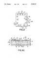
- FIG. 2is a plan view showing schematically an embodiment of the present invention
- FIG. 3Ais a plan view showing the embodiment of the present invention
- FIGS. 3B and 3Care cross-sectional views taken along lines B--B' and C--C' in FIG. 3A as viewed in the direction of arrows, respectively;
- FIG. 4is a plan view showing a modification of the embodiment of the present invention.
- FIG. 5is a cross-sectional view showing schematically in a state of installing the embodiment of the present invention within a package to complete a device.
- FIGS. 1A to 1Ca flip chip type semiconductor device having a favorable combination of apertures through which a solder bump is connected to a electrode pad thereunder will be explained.
- a thick field silicon oxide layer 3is thermally formed on a major surface of a P-type silicon substrate 1 .
- the field oxide layer 3consists of a first field silicon oxide layer 3' formed selectively in a circuit element forming portion 30 and a second field silicon oxide layer 3" formed entirely in a bump terminal forming portion 40.
- the boundary between the portions 30, 40is represented by a phantom line 50 in FIG. 1A, the first and second field oxide layers 3', 3" are continuously formed as shown in FIG. 1B.
- active regions of the substrate 1are surrounded by the first field oxide layer 3', and N-type impurity regions 2 are formed in the active regions.
- a plurality of internal wiring layers 10 including electrodes such as gate electrodesare formed with thin insulating films 4 including inter-ply insulating films on the first field oxide layer 3' and on the impurity regions 2 in the active regions.
- the internal wiring layersare connected each other at a contact part 12 and connected to the impurity regions 2 at contact parts 11.
- the impurity regions 2 and the internal wiring layers 10constitute circuit elements such as diodes, transistors, resistors, etc. and/or circuits.
- the circuit element forming portion 30is a portion where all of the internal wiring layers 10 and all of the active regions, the impurity regions 2 are formed, and that from the circuit element forming portion 30 only wiring layers 5, which are directly connected to bump terminal structures, can be led out.
- the second field oxide layer 3"is entirely formed such that any impurity region for forming a circuit element or a circuit is not provided, and electrode pads 15 of aluminum having 1.0 ⁇ m thickness are formed on the second field oxide layer 3".
- Each of the electrode pads 15has a square plan shape of 150 ⁇ m square and is connected to and is continuously formed with an aluminum wiring layer 5 having 1.0 ⁇ m thickness as a leading out or connecting means which is connected to the impurity region 2 constituting a circuit element in the circuit element forming portion 30.
- a silicon nitride film 6 of 1.0 to 1.5 ⁇ m thickness as an inorganic passivation insulating filmis entirely formed in the whole portions 30, 40, and openings 16 are formed in the silicon nitride film 6 on the electrode pads 15.
- Each of the openings 16has a square plan shape of 120 ⁇ m square, and therefore the upper surface of the electrode pad 15 is exposed in the same square shape.
- a polyimide film 7 of 1.0 ⁇ m thicknessis entirely formed in the openings 16 and on the silicon nitride film 6 in the whole portions 30, 40, and windows 17 are formed in the polyimide film 7 within the openings 16.
- Each of the windows 17has a circular plan shape of 80 ⁇ m diameter, and therefore the upper surface of the electrode pad 15 is exposed in the same circular shape.
- Barrier metal films 8are attached to the exposed upper surface of the electrode pads 15 through the circular window 17 and extend on the surface of the polyimide film 7 near the windows.
- Each of the barrier metal filmhas a circular plan shape of 150 ⁇ m diameter (not shown in FIG. 1A), and the center section of the upper surface of the barrier metal film 8 is shaped in a concavity having a circular plan shape due to the circular window 17 in the polyimide film 7.
- the barrier metal film 8may be a composite film consisting of a titanium film or a chromium film as a lower film and a copper film as an upper film.
- Spherical solder bump terminals 9made of eutectic alloy of lead (Pb) and tin (Sn) are formed on the barrier metal films 8.
- the barrier metal filmis attached to the electrode pad at the circular contact portion and the upper surface of the barrier metal film becomes the circular concavity shape, and therefore, the bottom of the solder bump terminal becomes also circular shape thereby forming the solder bump terminal with a desirable spherical shape and a small deviation of the height among the terminals in one semiconductor device.
- the rectangular opening in the inorganic passivation insulating filma beneficial mass-production of the device can be realized.
- the structure shown in FIG. 1has the polyimide film which is entirely formed on the circuit element forming portion 30, and therefore, the production yield and reliability of the device are inevitably reduced.
- the semiconductor device 80that is, a semiconductor pellet or a semiconductor chip includes the circuit element forming portion 30 and the bump terminal forming portion 40 surrounding substantially the portion 30.
- the bump terminal forming portion 40a plurality of bump terminals 9 are formed, and a plurality of polyimide films 27 are formed only near the bump terminals such that at least at the whole surface of the circuit element portion 30, the inorganic passivation layer 6 is exposed.
- a polyimide filmis entirely removed from the circuit element forming portion 30 and is selectively removed from the bump terminal forming portion 40 to remain the polyimide films 27 when the windows 17 are formed by a photo-lithography process step.
- Each of the polyimide films 27has the thickness ranging from 0.5 ⁇ m to 1.2 ⁇ m, for example, of 1.0 ⁇ m and a circular plan shape of the diameter ranging from 200 to 600 ⁇ m, for example, of 300 ⁇ m.
- the polyimide films 27are formed only above a part of leading out wiring layers, respectively, but the films 27 are never formed in the circuit element forming portion 30 of the pellet and the passivation insulating film 6 of inorganic material is entirely exposed in the portion 30. That is, the polyimide films 27 are never formed on any of the impurity regions 2 and on any of the internal wiring layers 10. Therefore, the disadvantages involved in the structure shown in FIG. 1 can be eliminated.
- the rectangular openings 16are formed in the inorganic passivation insulating film 6.
- an about 1 ⁇ m-thick polyimide filmis formed by spin coating on the entire upper surface of the inorganic passivation film 6 inclusive of the openings 16, and the portions of the film on the electrode pads 15 are etched and bored circularly by photographic technique and at the same time, all the areas other than the portions from the openings to the outer peripheral portions of the electrode pads 15 are exclusively etched in order to form the polyimide films 27 which has circular windows on the electrode pads 15 and covers the inorganic passivation film 6 only on the electrode pads 15 and on the inorganic passivation film 6 around the pads 15.
- This polyimide films 27are formed in such a manner as not to cover the circuit area.
- the barrier metal filmsuch as Ti-Cu, Cr-Cu or the like is formed on the electrode pads 15 and the polyimide films 27 and solder plating is selectively applied onto the electrode pads by use of a resist (not shown) for plating.
- the barrier metal filmis etched and successively to form the barrier metal films 8 shown in FIG. 3B, the solder-plated solder having mushroom-like figure is thermally fused and shaped (wet-back) to form the spherical solder bumps 9, thereby completing the flip chip type semiconductor device having the structure shown in FIG. 3B.
- the polyimide films 27 on the electrode pads 15are formed preferably in such a manner as to cover the edges of the openings 16 of the inorganic passivation film 6, too, so as to protect the electrode pads 15.
- FIG. 4a modification of the embodiment will be explained, and in the figure the same component as those in FIGS. 3A are indicated by the same reference numerals.
- An active region including an N-type impurity region 2'is formed between the bump terminal structures and an internal wiring layer 10' is connected to the impurity regions 2, 2' at contact parts 11', respectively. Therefore, the circuit element forming portion 30' becomes a convex plan shape and the bump terminal forming portion 40 becomes a concave plan shape with the boundary phantom line 50'. Further, the adjacent polyimide films are contacted on the passivation insulating layer 6 to form a combined polyimide film 27' belonging to two of bonding bump structures.
- the polyimide films 27 including the combined polyimide film 27'are never elongated into the circuit element forming portion 30'.
- the circuit areadoes not exist between the adjacent electrode pads and when it is difficult to form individually the polyimide films, these polyimide films are integrated as the polyimide film 27'.
- the semiconductor pellet 80 according to the present inventionis installed in a hermetically sealing type package such as a ceramic package or a glass-sealed package in which inert gas or air is sealed.
- a hermetically sealing type packagesuch as a ceramic package or a glass-sealed package in which inert gas or air is sealed.
- FIG. 5exemplifies a ceramic package 90 which comprises a ceramic body 91, outer leads 92, a weld ring 93, a lid 94, metallized lead layers 96, 97 and bonding wires 98.
- the packageis sealed by welding the lid 94 to the weld ring 93 at the portion 95, and in the package nitrogen gas 99 is filled so that the inorganic passivation insulating layer 6 in the circuit forming portion 30 of the pellet 80 is exposed to the nitrogen gas 99.
Landscapes
- Engineering & Computer Science (AREA)
- Computer Hardware Design (AREA)
- Microelectronics & Electronic Packaging (AREA)
- Power Engineering (AREA)
- Internal Circuitry In Semiconductor Integrated Circuit Devices (AREA)
- Formation Of Insulating Films (AREA)
Abstract
Description
Claims (10)
Applications Claiming Priority (2)
| Application Number | Priority Date | Filing Date | Title |
|---|---|---|---|
| JP63-41180 | 1988-02-23 | ||
| JP63041180AJPH01214141A (en) | 1988-02-23 | 1988-02-23 | Flip-chip type semiconductor device |
Publications (1)
| Publication Number | Publication Date |
|---|---|
| US5046161Atrue US5046161A (en) | 1991-09-03 |
Family
ID=12601231
Family Applications (1)
| Application Number | Title | Priority Date | Filing Date |
|---|---|---|---|
| US07/314,166Expired - LifetimeUS5046161A (en) | 1988-02-23 | 1989-02-22 | Flip chip type semiconductor device |
Country Status (2)
| Country | Link |
|---|---|
| US (1) | US5046161A (en) |
| JP (1) | JPH01214141A (en) |
Cited By (71)
| Publication number | Priority date | Publication date | Assignee | Title |
|---|---|---|---|---|
| US5438216A (en)* | 1992-08-31 | 1995-08-01 | Motorola, Inc. | Light erasable multichip module |
| US5539153A (en)* | 1994-08-08 | 1996-07-23 | Hewlett-Packard Company | Method of bumping substrates by contained paste deposition |
| US5726501A (en)* | 1994-11-22 | 1998-03-10 | Sharp Kabushiki Kaisha | Semiconductor device having a solder drawing layer |
| US5834844A (en)* | 1995-03-24 | 1998-11-10 | Shinko Electric Industries Co., Ltd. | Semiconductor device having an element with circuit pattern thereon |
| US5854513A (en)* | 1995-07-14 | 1998-12-29 | Lg Electronics Inc. | Semiconductor device having a bump structure and test electrode |
| US5912510A (en)* | 1996-05-29 | 1999-06-15 | Motorola, Inc. | Bonding structure for an electronic device |
| US5956605A (en)* | 1996-09-20 | 1999-09-21 | Micron Technology, Inc. | Use of nitrides for flip-chip encapsulation |
| US5977641A (en)* | 1997-05-14 | 1999-11-02 | Kabushiki Kaisha Toshiba | Semiconductor device and method for manufacturing the same |
| US5994783A (en)* | 1996-09-11 | 1999-11-30 | Lg Semicon Co., Ltd. | Semiconductor chip package and fabrication method thereof |
| US6002172A (en)* | 1997-03-12 | 1999-12-14 | International Business Machines Corporation | Substrate structure and method for improving attachment reliability of semiconductor chips and modules |
| US6025767A (en)* | 1996-08-05 | 2000-02-15 | Mcnc | Encapsulated micro-relay modules and methods of fabricating same |
| US6111317A (en)* | 1996-01-18 | 2000-08-29 | Kabushiki Kaisha Toshiba | Flip-chip connection type semiconductor integrated circuit device |
| US6157079A (en)* | 1997-11-10 | 2000-12-05 | Citizen Watch Co., Ltd | Semiconductor device with a bump including a bump electrode film covering a projecting photoresist |
| US6222212B1 (en) | 1994-01-27 | 2001-04-24 | Integrated Device Technology, Inc. | Semiconductor device having programmable interconnect layers |
| US6293456B1 (en) | 1997-05-27 | 2001-09-25 | Spheretek, Llc | Methods for forming solder balls on substrates |
| US6329608B1 (en) | 1995-04-05 | 2001-12-11 | Unitive International Limited | Key-shaped solder bumps and under bump metallurgy |
| US6388203B1 (en) | 1995-04-04 | 2002-05-14 | Unitive International Limited | Controlled-shaped solder reservoirs for increasing the volume of solder bumps, and structures formed thereby |
| US6437432B2 (en)* | 2000-03-21 | 2002-08-20 | Fujitsu Limited | Semiconductor device having improved electrical characteristics and method of producing the same |
| US6472761B2 (en)* | 2000-03-15 | 2002-10-29 | Sharp Kabushiki Kaisha | Solid-state image pickup apparatus and manufacturing method thereof |
| US6498396B1 (en)* | 1995-03-30 | 2002-12-24 | Mitsubishi Denki Kabushiki Kaisha | Semiconductor chip scale package and ball grid array structures |
| US6512298B2 (en)* | 2000-11-29 | 2003-01-28 | Matsushita Electric Industrial Co., Ltd. | Semiconductor device and method for producing the same |
| US20030045015A1 (en)* | 2001-07-23 | 2003-03-06 | Slater David B. | Flip-chip bonding of light emitting devices and light emitting devices suitable for flip-chip bonding |
| US20030089969A1 (en)* | 1997-01-17 | 2003-05-15 | Seiko Epson Corporation | Electronic component, semiconductor device, methods of manufacturing the same, circuit board, and electronic instrument |
| US20030098505A1 (en)* | 2001-11-26 | 2003-05-29 | Junichi Kimura | Semiconductor module |
| US20030148604A1 (en)* | 2001-12-13 | 2003-08-07 | Mou-Shiung Lin | Chip structure and process for forming the same |
| US6609652B2 (en) | 1997-05-27 | 2003-08-26 | Spheretek, Llc | Ball bumping substrates, particuarly wafers |
| US6747298B2 (en) | 2001-07-23 | 2004-06-08 | Cree, Inc. | Collets for bonding of light emitting diodes having shaped substrates |
| US20050136641A1 (en)* | 2003-10-14 | 2005-06-23 | Rinne Glenn A. | Solder structures for out of plane connections and related methods |
| US20050150936A1 (en)* | 1997-05-27 | 2005-07-14 | Mackay John | Bumping electronic components using transfer substrates |
| US20050194687A1 (en)* | 2002-08-21 | 2005-09-08 | Seiko Epson Corporation | Semiconductor device, method of manufacturing the same, circuit board, and electronic instrument |
| US6960828B2 (en) | 2002-06-25 | 2005-11-01 | Unitive International Limited | Electronic structures including conductive shunt layers |
| US7007833B2 (en) | 1997-05-27 | 2006-03-07 | Mackay John | Forming solder balls on substrates |
| US20060060961A1 (en)* | 2004-07-09 | 2006-03-23 | Mou-Shiung Lin | Chip structure |
| US20060148247A1 (en)* | 2003-01-06 | 2006-07-06 | Megic Corporation | Method of metal sputtering for integrated circuit metal routing |
| US7081404B2 (en) | 2003-02-18 | 2006-07-25 | Unitive Electronics Inc. | Methods of selectively bumping integrated circuit substrates and related structures |
| US7156284B2 (en) | 2000-12-15 | 2007-01-02 | Unitive International Limited | Low temperature methods of bonding components and related structures |
| US7213740B2 (en) | 2000-11-10 | 2007-05-08 | Unitive International Limited | Optical structures including liquid bumps and related methods |
| US20070197016A1 (en)* | 2006-02-17 | 2007-08-23 | Fujitsu Limited | Semiconductor device and manufacturing method for the same |
| US20070273035A1 (en)* | 1998-12-21 | 2007-11-29 | Mou-Shiung Lin | Top layers of metal for high performance IC's |
| US20080001300A1 (en)* | 2000-10-18 | 2008-01-03 | Megica Corporation | Post passivation interconnection schemes on top of IC chip |
| US20080042273A1 (en)* | 1998-12-21 | 2008-02-21 | Megica Corporation | High performance system-on-chip using post passivation process |
| US20080048328A1 (en)* | 2001-12-13 | 2008-02-28 | Megica Corporation | Chip structure and process for forming the same |
| US20080048320A1 (en)* | 2001-03-05 | 2008-02-28 | Megica Corporation | Low fabrication cost, fine pitch and high reliability solder bump |
| US20080050912A1 (en)* | 1998-12-21 | 2008-02-28 | Megica Corporation | Chip structure and process for forming the same |
| US20080067677A1 (en)* | 2001-03-05 | 2008-03-20 | Megica Corporation | Structure and manufacturing method of a chip scale package |
| US20080081458A1 (en)* | 2006-09-29 | 2008-04-03 | Megica Corporation | Integrated circuit chips with fine-line metal and over-passivation metal |
| US7358174B2 (en) | 2004-04-13 | 2008-04-15 | Amkor Technology, Inc. | Methods of forming solder bumps on exposed metal pads |
| US20080087709A1 (en)* | 1997-05-27 | 2008-04-17 | Mackay John | Bumping Electronic Components Using Transfer Substrates |
| US20080113504A1 (en)* | 2002-05-01 | 2008-05-15 | Megica Corporation | Low fabrication cost, high performance, high reliability chip scale package |
| US20080121943A1 (en)* | 1998-12-21 | 2008-05-29 | Mou-Shiung Lin | Top layers of metal for integrated circuits |
| US20080128910A1 (en)* | 2004-09-09 | 2008-06-05 | Megica Corporation | Post Passivation Interconnection Process And Structures |
| US20080246154A1 (en)* | 1998-12-21 | 2008-10-09 | Megica Corporation | Top layers of metal for high performance IC's |
| US20080251924A1 (en)* | 2003-10-15 | 2008-10-16 | Megica Corporation | Post Passivation Interconnection Schemes On Top Of The IC Chips |
| US20080251925A1 (en)* | 2004-09-23 | 2008-10-16 | Megica Corporation | Top layers of metal for integrated circuits |
| US20080290520A1 (en)* | 2004-09-09 | 2008-11-27 | Megica Corporation | Reliable metal bumps on top of I/O pads after removal of test probe marks |
| US20090001511A1 (en)* | 2005-03-29 | 2009-01-01 | Megica Corporation | High performance system-on-chip using post passivation process |
| US20090057894A1 (en)* | 2004-07-09 | 2009-03-05 | Megica Corporation | Structure of Gold Bumps and Gold Conductors on one IC Die and Methods of Manufacturing the Structures |
| US7531898B2 (en) | 2002-06-25 | 2009-05-12 | Unitive International Limited | Non-Circular via holes for bumping pads and related structures |
| US20090146305A1 (en)* | 2004-10-12 | 2009-06-11 | Megica Corporation | Post passivation interconnection schemes on top of the ic chips |
| US7547623B2 (en) | 2002-06-25 | 2009-06-16 | Unitive International Limited | Methods of forming lead free solder bumps |
| US7654432B2 (en) | 1997-05-27 | 2010-02-02 | Wstp, Llc | Forming solder balls on substrates |
| US7674701B2 (en) | 2006-02-08 | 2010-03-09 | Amkor Technology, Inc. | Methods of forming metal layers using multi-layer lift-off patterns |
| US20110092066A1 (en)* | 1997-05-27 | 2011-04-21 | Mackay John | Bumping Electronic Components Using Transfer Substrates |
| US7932615B2 (en) | 2006-02-08 | 2011-04-26 | Amkor Technology, Inc. | Electronic devices including solder bumps on compliant dielectric layers |
| US7960270B2 (en) | 2002-01-07 | 2011-06-14 | Megica Corporation | Method for fabricating circuit component |
| US8008775B2 (en) | 2004-09-09 | 2011-08-30 | Megica Corporation | Post passivation interconnection structures |
| US8178967B2 (en) | 2001-09-17 | 2012-05-15 | Megica Corporation | Low fabrication cost, high performance, high reliability chip scale package |
| US8901733B2 (en) | 2001-02-15 | 2014-12-02 | Qualcomm Incorporated | Reliable metal bumps on top of I/O pads after removal of test probe marks |
| US20150098224A1 (en)* | 2013-10-08 | 2015-04-09 | Lg Innotek Co., Ltd. | Light emitting device, light emitting device package including the device and lighting apparatus including the package |
| US9105463B2 (en) | 2011-11-10 | 2015-08-11 | Panasonic Corporation | Semiconductor device |
| US20180366377A1 (en)* | 2014-04-17 | 2018-12-20 | Lg Display Co., Ltd. | Array substrate for display device and manufacturing method thereof |
Citations (18)
| Publication number | Priority date | Publication date | Assignee | Title |
|---|---|---|---|---|
| US3902148A (en)* | 1970-11-27 | 1975-08-26 | Signetics Corp | Semiconductor lead structure and assembly and method for fabricating same |
| JPS5368970A (en)* | 1976-12-01 | 1978-06-19 | Hitachi Ltd | Solder electrode structure |
| JPS54162458A (en)* | 1978-06-13 | 1979-12-24 | Matsushita Electric Ind Co Ltd | Manufacture for semiconductor device |
| US4205099A (en)* | 1978-04-14 | 1980-05-27 | Sprague Electric Company | Method for making terminal bumps on semiconductor wafers |
| US4224002A (en)* | 1978-08-04 | 1980-09-23 | Amerace Corporation | Highway delineator |
| JPS55156339A (en)* | 1979-05-25 | 1980-12-05 | Hitachi Ltd | Forming method of bump electrode |
| JPS56147464A (en)* | 1980-04-17 | 1981-11-16 | Fujitsu Ltd | Forming method for soldering terminal portion of thin film element |
| JPS5773952A (en)* | 1980-10-27 | 1982-05-08 | Hitachi Ltd | Chip for face down bonding and production thereof |
| EP0061593A2 (en)* | 1981-03-30 | 1982-10-06 | International Business Machines Corporation | Solder support pad for semiconductor devices |
| JPS58200526A (en)* | 1982-05-18 | 1983-11-22 | Citizen Watch Co Ltd | Semiconductor device having multi-layer wirings |
| EP0122631A2 (en)* | 1983-04-15 | 1984-10-24 | Hitachi, Ltd. | Electronic device having a multi-layer wiring structure |
| US4514751A (en)* | 1982-12-23 | 1985-04-30 | International Business Machines Corporation | Compressively stresses titanium metallurgy for contacting passivated semiconductor devices |
| US4618878A (en)* | 1983-06-18 | 1986-10-21 | Kabushiki Kaisha Toshiba | Semiconductor device having a multilayer wiring structure using a polyimide resin |
| JPS62128154A (en)* | 1985-11-28 | 1987-06-10 | Fujitsu Ltd | Manufacturing method of semiconductor device |
| US4706106A (en)* | 1984-06-14 | 1987-11-10 | Mitsubishi Denki Kabushiki Kaisha | Semiconductor light receiving device |
| US4733289A (en)* | 1980-04-25 | 1988-03-22 | Hitachi, Ltd. | Resin-molded semiconductor device using polyimide and nitride films for the passivation film |
| US4761386A (en)* | 1984-10-22 | 1988-08-02 | National Semiconductor Corporation | Method of fabricating conductive non-metallic self-passivating non-corrodable IC bonding pads |
| JPS63318742A (en)* | 1987-06-22 | 1988-12-27 | Hitachi Ltd | Semiconductor integrated circuit device and its manufacturing method |
- 1988
- 1988-02-23JPJP63041180Apatent/JPH01214141A/enactivePending
- 1989
- 1989-02-22USUS07/314,166patent/US5046161A/ennot_activeExpired - Lifetime
Patent Citations (18)
| Publication number | Priority date | Publication date | Assignee | Title |
|---|---|---|---|---|
| US3902148A (en)* | 1970-11-27 | 1975-08-26 | Signetics Corp | Semiconductor lead structure and assembly and method for fabricating same |
| JPS5368970A (en)* | 1976-12-01 | 1978-06-19 | Hitachi Ltd | Solder electrode structure |
| US4205099A (en)* | 1978-04-14 | 1980-05-27 | Sprague Electric Company | Method for making terminal bumps on semiconductor wafers |
| JPS54162458A (en)* | 1978-06-13 | 1979-12-24 | Matsushita Electric Ind Co Ltd | Manufacture for semiconductor device |
| US4224002A (en)* | 1978-08-04 | 1980-09-23 | Amerace Corporation | Highway delineator |
| JPS55156339A (en)* | 1979-05-25 | 1980-12-05 | Hitachi Ltd | Forming method of bump electrode |
| JPS56147464A (en)* | 1980-04-17 | 1981-11-16 | Fujitsu Ltd | Forming method for soldering terminal portion of thin film element |
| US4733289A (en)* | 1980-04-25 | 1988-03-22 | Hitachi, Ltd. | Resin-molded semiconductor device using polyimide and nitride films for the passivation film |
| JPS5773952A (en)* | 1980-10-27 | 1982-05-08 | Hitachi Ltd | Chip for face down bonding and production thereof |
| EP0061593A2 (en)* | 1981-03-30 | 1982-10-06 | International Business Machines Corporation | Solder support pad for semiconductor devices |
| JPS58200526A (en)* | 1982-05-18 | 1983-11-22 | Citizen Watch Co Ltd | Semiconductor device having multi-layer wirings |
| US4514751A (en)* | 1982-12-23 | 1985-04-30 | International Business Machines Corporation | Compressively stresses titanium metallurgy for contacting passivated semiconductor devices |
| EP0122631A2 (en)* | 1983-04-15 | 1984-10-24 | Hitachi, Ltd. | Electronic device having a multi-layer wiring structure |
| US4618878A (en)* | 1983-06-18 | 1986-10-21 | Kabushiki Kaisha Toshiba | Semiconductor device having a multilayer wiring structure using a polyimide resin |
| US4706106A (en)* | 1984-06-14 | 1987-11-10 | Mitsubishi Denki Kabushiki Kaisha | Semiconductor light receiving device |
| US4761386A (en)* | 1984-10-22 | 1988-08-02 | National Semiconductor Corporation | Method of fabricating conductive non-metallic self-passivating non-corrodable IC bonding pads |
| JPS62128154A (en)* | 1985-11-28 | 1987-06-10 | Fujitsu Ltd | Manufacturing method of semiconductor device |
| JPS63318742A (en)* | 1987-06-22 | 1988-12-27 | Hitachi Ltd | Semiconductor integrated circuit device and its manufacturing method |
Non-Patent Citations (4)
| Title |
|---|
| Marc Wittmer, "Barrier Layers: Principles and Applications in Microelectronics", J. Vac. Sci. Technology, Apr.-Jun. 84, pp. 273-280. |
| Marc Wittmer, Barrier Layers: Principles and Applications in Microelectronics , J. Vac. Sci. Technology, Apr. Jun. 84, pp. 273 280.* |
| Noubel et al, "Metallurgy Including a Chromium Slice", IBM Technical Disclosure, vol. 11, No. 7, Dec./68, p. 769. |
| Noubel et al, Metallurgy Including a Chromium Slice , IBM Technical Disclosure, vol. 11, No. 7, Dec./68, p. 769.* |
Cited By (210)
| Publication number | Priority date | Publication date | Assignee | Title |
|---|---|---|---|---|
| US5438216A (en)* | 1992-08-31 | 1995-08-01 | Motorola, Inc. | Light erasable multichip module |
| US6222212B1 (en) | 1994-01-27 | 2001-04-24 | Integrated Device Technology, Inc. | Semiconductor device having programmable interconnect layers |
| US5539153A (en)* | 1994-08-08 | 1996-07-23 | Hewlett-Packard Company | Method of bumping substrates by contained paste deposition |
| US5586715A (en)* | 1994-08-08 | 1996-12-24 | Hewlett-Packard Company | Method of making solder balls by contained paste deposition |
| US5672542A (en)* | 1994-08-08 | 1997-09-30 | Hewlett Packard Company | Method of making solder balls by contained paste deposition |
| US5726501A (en)* | 1994-11-22 | 1998-03-10 | Sharp Kabushiki Kaisha | Semiconductor device having a solder drawing layer |
| EP0714123A3 (en)* | 1994-11-22 | 1998-06-10 | Sharp Kabushiki Kaisha | A semiconductor device, a semiconductor device-mounted apparatus, and a method for replacing the semiconductor device |
| US5960308A (en)* | 1995-03-24 | 1999-09-28 | Shinko Electric Industries Co. Ltd. | Process for making a chip sized semiconductor device |
| US5834844A (en)* | 1995-03-24 | 1998-11-10 | Shinko Electric Industries Co., Ltd. | Semiconductor device having an element with circuit pattern thereon |
| US6498396B1 (en)* | 1995-03-30 | 2002-12-24 | Mitsubishi Denki Kabushiki Kaisha | Semiconductor chip scale package and ball grid array structures |
| US6392163B1 (en) | 1995-04-04 | 2002-05-21 | Unitive International Limited | Controlled-shaped solder reservoirs for increasing the volume of solder bumps |
| US6388203B1 (en) | 1995-04-04 | 2002-05-14 | Unitive International Limited | Controlled-shaped solder reservoirs for increasing the volume of solder bumps, and structures formed thereby |
| US6329608B1 (en) | 1995-04-05 | 2001-12-11 | Unitive International Limited | Key-shaped solder bumps and under bump metallurgy |
| US6389691B1 (en) | 1995-04-05 | 2002-05-21 | Unitive International Limited | Methods for forming integrated redistribution routing conductors and solder bumps |
| US5854513A (en)* | 1995-07-14 | 1998-12-29 | Lg Electronics Inc. | Semiconductor device having a bump structure and test electrode |
| US6111317A (en)* | 1996-01-18 | 2000-08-29 | Kabushiki Kaisha Toshiba | Flip-chip connection type semiconductor integrated circuit device |
| US5912510A (en)* | 1996-05-29 | 1999-06-15 | Motorola, Inc. | Bonding structure for an electronic device |
| US6025767A (en)* | 1996-08-05 | 2000-02-15 | Mcnc | Encapsulated micro-relay modules and methods of fabricating same |
| US5994783A (en)* | 1996-09-11 | 1999-11-30 | Lg Semicon Co., Ltd. | Semiconductor chip package and fabrication method thereof |
| US6277670B1 (en) | 1996-09-11 | 2001-08-21 | Hyundai Electronics Industries Co., Ltd. | Semiconductor chip package and fabrication method thereof |
| CN1085890C (en)* | 1996-09-11 | 2002-05-29 | Lg半导体株式会社 | Chip-size semiconductor package and fabrication method thereof |
| US5956605A (en)* | 1996-09-20 | 1999-09-21 | Micron Technology, Inc. | Use of nitrides for flip-chip encapsulation |
| US6972249B2 (en) | 1996-09-20 | 2005-12-06 | Micron Technology, Inc. | Use of nitrides for flip-chip encapsulation |
| US20030137062A1 (en)* | 1996-09-20 | 2003-07-24 | Salman Akram | Use of nitrides for flip-chip encapsulation |
| US6528894B1 (en) | 1996-09-20 | 2003-03-04 | Micron Technology, Inc. | Use of nitrides for flip-chip encapsulation |
| US20100240176A1 (en)* | 1997-01-17 | 2010-09-23 | Seiko Epson Corporation | Electronic component, semiconductor device, methods of manufacturing the same, circuit board, and electronic instrument |
| US20030089969A1 (en)* | 1997-01-17 | 2003-05-15 | Seiko Epson Corporation | Electronic component, semiconductor device, methods of manufacturing the same, circuit board, and electronic instrument |
| US7888177B2 (en) | 1997-01-17 | 2011-02-15 | Seiko Epson Corporation | Electronic component, semiconductor device, methods of manufacturing the same, circuit board, and electronic instrument |
| US20110095422A1 (en)* | 1997-01-17 | 2011-04-28 | Seiko Epson Corporation | Electronic component, semiconductor device, methods of manufacturing the same, circuit board, and electronic instrument |
| US20080079162A1 (en)* | 1997-01-17 | 2008-04-03 | Seiko Epson Corporation | Electronic component, semiconductor device, methods of manufacturing the same, circuit board, and electronic instrument |
| US20090111260A1 (en)* | 1997-01-17 | 2009-04-30 | Seiko Epson Corporation | Electronic component, semiconductor device, methods of manufacturing the same, circuit board, and electronic instrument |
| US7485973B2 (en) | 1997-01-17 | 2009-02-03 | Seiko Epson Corporation | Electronic component, semiconductor device, methods of manufacturing the same, circuit board, and electronic instrument |
| US8399999B2 (en) | 1997-01-17 | 2013-03-19 | Seiko Epson Corporation | Electronic component, semiconductor device, methods of manufacturing the same, circuit board, and electronic instrument |
| US7307351B2 (en) | 1997-01-17 | 2007-12-11 | Seiko Epson Corporation | Electronic component, semiconductor device, methods of manufacturing the same, circuit board, and electronic instrument |
| US7235881B2 (en)* | 1997-01-17 | 2007-06-26 | Seiko Epson Corporation | Electronic component, semiconductor device, methods of manufacturing the same, circuit board, and electronic instrument |
| US7755205B2 (en) | 1997-01-17 | 2010-07-13 | Seiko Epson Corporation | Electronic component, semiconductor device, methods of manufacturing the same, circuit board, and electronic instrument |
| US20070187825A1 (en)* | 1997-01-17 | 2007-08-16 | Seiko Epson Corporation | Electronic component, semiconductor device, methods of manufacturing the same, circuit board, and electronic instrument |
| US6281581B1 (en) | 1997-03-12 | 2001-08-28 | International Business Machines Corporation | Substrate structure for improving attachment reliability of semiconductor chips and modules |
| US6002172A (en)* | 1997-03-12 | 1999-12-14 | International Business Machines Corporation | Substrate structure and method for improving attachment reliability of semiconductor chips and modules |
| US6251766B1 (en) | 1997-03-12 | 2001-06-26 | International Business Machines Corporation | Method for improving attachment reliability of semiconductor chips and modules |
| US5977641A (en)* | 1997-05-14 | 1999-11-02 | Kabushiki Kaisha Toshiba | Semiconductor device and method for manufacturing the same |
| US6153448A (en)* | 1997-05-14 | 2000-11-28 | Kabushiki Kaisha Toshiba | Semiconductor device manufacturing method |
| US7288471B2 (en) | 1997-05-27 | 2007-10-30 | Mackay John | Bumping electronic components using transfer substrates |
| US20060208041A1 (en)* | 1997-05-27 | 2006-09-21 | Mackay John | Forming solder balls on substrates |
| US7654432B2 (en) | 1997-05-27 | 2010-02-02 | Wstp, Llc | Forming solder balls on substrates |
| US20050150936A1 (en)* | 1997-05-27 | 2005-07-14 | Mackay John | Bumping electronic components using transfer substrates |
| US20110092066A1 (en)* | 1997-05-27 | 2011-04-21 | Mackay John | Bumping Electronic Components Using Transfer Substrates |
| US6293456B1 (en) | 1997-05-27 | 2001-09-25 | Spheretek, Llc | Methods for forming solder balls on substrates |
| US7007833B2 (en) | 1997-05-27 | 2006-03-07 | Mackay John | Forming solder balls on substrates |
| US20080087709A1 (en)* | 1997-05-27 | 2008-04-17 | Mackay John | Bumping Electronic Components Using Transfer Substrates |
| US7604153B2 (en) | 1997-05-27 | 2009-10-20 | Wstp, Llc | Forming solder balls on substrates |
| US7819301B2 (en) | 1997-05-27 | 2010-10-26 | Wstp, Llc | Bumping electronic components using transfer substrates |
| US6609652B2 (en) | 1997-05-27 | 2003-08-26 | Spheretek, Llc | Ball bumping substrates, particuarly wafers |
| US6157079A (en)* | 1997-11-10 | 2000-12-05 | Citizen Watch Co., Ltd | Semiconductor device with a bump including a bump electrode film covering a projecting photoresist |
| US20080124918A1 (en)* | 1998-12-21 | 2008-05-29 | Megica Corporation | Chip structure and process for forming the same |
| US8304907B2 (en) | 1998-12-21 | 2012-11-06 | Megica Corporation | Top layers of metal for integrated circuits |
| US20090146307A1 (en)* | 1998-12-21 | 2009-06-11 | Megica Corporation | Top layers of metal for high performance IC's |
| US7999384B2 (en) | 1998-12-21 | 2011-08-16 | Megica Corporation | Top layers of metal for high performance IC's |
| US8022545B2 (en) | 1998-12-21 | 2011-09-20 | Megica Corporation | Top layers of metal for high performance IC's |
| US7915157B2 (en) | 1998-12-21 | 2011-03-29 | Megica Corporation | Chip structure and process for forming the same |
| US8487400B2 (en) | 1998-12-21 | 2013-07-16 | Megica Corporation | High performance system-on-chip using post passivation process |
| US20080246154A1 (en)* | 1998-12-21 | 2008-10-09 | Megica Corporation | Top layers of metal for high performance IC's |
| US7906422B2 (en) | 1998-12-21 | 2011-03-15 | Megica Corporation | Chip structure and process for forming the same |
| US20080121943A1 (en)* | 1998-12-21 | 2008-05-29 | Mou-Shiung Lin | Top layers of metal for integrated circuits |
| US20080093745A1 (en)* | 1998-12-21 | 2008-04-24 | Megica Corporation | High performance system-on-chip using post passivation process |
| US20070273035A1 (en)* | 1998-12-21 | 2007-11-29 | Mou-Shiung Lin | Top layers of metal for high performance IC's |
| US7906849B2 (en) | 1998-12-21 | 2011-03-15 | Megica Corporation | Chip structure and process for forming the same |
| US20070290368A1 (en)* | 1998-12-21 | 2007-12-20 | Mou-Shiung Lin | Top layers of metal for high performance IC's |
| US8531038B2 (en) | 1998-12-21 | 2013-09-10 | Megica Corporation | Top layers of metal for high performance IC's |
| US8471384B2 (en) | 1998-12-21 | 2013-06-25 | Megica Corporation | Top layers of metal for high performance IC's |
| US8415800B2 (en) | 1998-12-21 | 2013-04-09 | Megica Corporation | Top layers of metal for high performance IC's |
| US8022546B2 (en) | 1998-12-21 | 2011-09-20 | Megica Corporation | Top layers of metal for high performance IC's |
| US20080042273A1 (en)* | 1998-12-21 | 2008-02-21 | Megica Corporation | High performance system-on-chip using post passivation process |
| US8350386B2 (en) | 1998-12-21 | 2013-01-08 | Megica Corporation | Top layers of metal for high performance IC's |
| US20080044977A1 (en)* | 1998-12-21 | 2008-02-21 | Megica Corporation | High performance system-on-chip using post passivation process |
| US8035227B2 (en) | 1998-12-21 | 2011-10-11 | Megica Corporation | Top layers of metal for high performance IC's |
| US8368204B2 (en) | 1998-12-21 | 2013-02-05 | Megica Corporation | Chip structure and process for forming the same |
| US20080042239A1 (en)* | 1998-12-21 | 2008-02-21 | Megica Corporation | High performance system-on-chip using post passivation process |
| US7884479B2 (en) | 1998-12-21 | 2011-02-08 | Megica Corporation | Top layers of metal for high performance IC's |
| US20080136034A1 (en)* | 1998-12-21 | 2008-06-12 | Megica Corporation | Chip structure and process for forming the same |
| US20100117236A1 (en)* | 1998-12-21 | 2010-05-13 | Megica Corporation | Top layers of metal for high performance ic's |
| US20080050912A1 (en)* | 1998-12-21 | 2008-02-28 | Megica Corporation | Chip structure and process for forming the same |
| US20080142981A1 (en)* | 1998-12-21 | 2008-06-19 | Mou-Shiung Lin | Top layers of metal for high performance IC's |
| US7863654B2 (en) | 1998-12-21 | 2011-01-04 | Megica Corporation | Top layers of metal for high performance IC's |
| US6472761B2 (en)* | 2000-03-15 | 2002-10-29 | Sharp Kabushiki Kaisha | Solid-state image pickup apparatus and manufacturing method thereof |
| US6437432B2 (en)* | 2000-03-21 | 2002-08-20 | Fujitsu Limited | Semiconductor device having improved electrical characteristics and method of producing the same |
| US8461686B2 (en) | 2000-10-18 | 2013-06-11 | Megica Corporation | Post passivation interconnection schemes on top of IC chip |
| US7902067B2 (en) | 2000-10-18 | 2011-03-08 | Megica Corporation | Post passivation interconnection schemes on top of the IC chips |
| US20080045001A1 (en)* | 2000-10-18 | 2008-02-21 | Megica Corporation | Post passivation interconnection schemes on top of IC chip |
| US20080045002A1 (en)* | 2000-10-18 | 2008-02-21 | Megica Corporation | Post passivation interconnection schemes on top of IC chip |
| US20080045008A1 (en)* | 2000-10-18 | 2008-02-21 | Megica Corporation | Post passivation interconnection schemes on top of IC chip |
| US20080042294A1 (en)* | 2000-10-18 | 2008-02-21 | Megica Corporation | Post passivation interconnection schemes on top of IC chip |
| US20080032496A1 (en)* | 2000-10-18 | 2008-02-07 | Megica Corporation | Post passivation interconnection schemes on top of the IC chips |
| US20080003806A1 (en)* | 2000-10-18 | 2008-01-03 | Megica Corporation | Post passivation interconnection schemes on top of IC chip |
| USRE43674E1 (en) | 2000-10-18 | 2012-09-18 | Megica Corporation | Post passivation metal scheme for high-performance integrated circuit devices |
| US20080001300A1 (en)* | 2000-10-18 | 2008-01-03 | Megica Corporation | Post passivation interconnection schemes on top of IC chip |
| US8435883B2 (en) | 2000-10-18 | 2013-05-07 | Megica Corporation | Post passivation interconnection schemes on top of IC chips |
| US20080061444A1 (en)* | 2000-10-18 | 2008-03-13 | Megica Corporation | Post passivation interconnection schemes on top of IC chip |
| US20080067694A1 (en)* | 2000-10-18 | 2008-03-20 | Megica Corporation | Post passivation interconnection schemes on top of IC chip |
| US8188603B2 (en) | 2000-10-18 | 2012-05-29 | Megica Corporation | Post passivation interconnection schemes on top of IC chip |
| US7923366B2 (en) | 2000-10-18 | 2011-04-12 | Megica Corporation | Post passivation interconnection schemes on top of IC chip |
| US8482127B2 (en) | 2000-10-18 | 2013-07-09 | Megica Corporation | Post passivation interconnection schemes on top of IC chip |
| US8492900B2 (en) | 2000-10-18 | 2013-07-23 | Megica Corporation | Post passivation interconnection schemes on top of IC chip |
| US8004088B2 (en) | 2000-10-18 | 2011-08-23 | Megica Corporation | Post passivation interconnection schemes on top of IC chip |
| US20080067686A1 (en)* | 2000-10-18 | 2008-03-20 | Megica Corporation | Post passivation interconnection schemes on top of IC chip |
| US7915161B2 (en) | 2000-10-18 | 2011-03-29 | Megica Corporation | Post passivation interconnection schemes on top of IC chip |
| US7919865B2 (en) | 2000-10-18 | 2011-04-05 | Megica Corporation | Post passivation interconnection schemes on top of IC chip |
| US7892965B2 (en) | 2000-10-18 | 2011-02-22 | Megica Corporation | Post passivation interconnection schemes on top of IC chip |
| US7213740B2 (en) | 2000-11-10 | 2007-05-08 | Unitive International Limited | Optical structures including liquid bumps and related methods |
| US6512298B2 (en)* | 2000-11-29 | 2003-01-28 | Matsushita Electric Industrial Co., Ltd. | Semiconductor device and method for producing the same |
| US7156284B2 (en) | 2000-12-15 | 2007-01-02 | Unitive International Limited | Low temperature methods of bonding components and related structures |
| US8901733B2 (en) | 2001-02-15 | 2014-12-02 | Qualcomm Incorporated | Reliable metal bumps on top of I/O pads after removal of test probe marks |
| US8072070B2 (en) | 2001-03-05 | 2011-12-06 | Megica Corporation | Low fabrication cost, fine pitch and high reliability solder bump |
| US20080048320A1 (en)* | 2001-03-05 | 2008-02-28 | Megica Corporation | Low fabrication cost, fine pitch and high reliability solder bump |
| US7902679B2 (en) | 2001-03-05 | 2011-03-08 | Megica Corporation | Structure and manufacturing method of a chip scale package with low fabrication cost, fine pitch and high reliability solder bump |
| US7863739B2 (en) | 2001-03-05 | 2011-01-04 | Megica Corporation | Low fabrication cost, fine pitch and high reliability solder bump |
| US20080054459A1 (en)* | 2001-03-05 | 2008-03-06 | Megica Corporation | Low fabrication cost, fine pitch and high reliability solder bump |
| US8158508B2 (en) | 2001-03-05 | 2012-04-17 | Megica Corporation | Structure and manufacturing method of a chip scale package |
| US20090267213A1 (en)* | 2001-03-05 | 2009-10-29 | Megica Corporation | Structure and manufacturing method of a chip scale package with low fabrication cost, fine pitch and high reliability solder bump |
| US20090261473A1 (en)* | 2001-03-05 | 2009-10-22 | Megica Corporation | Low fabrication cost, fine pitch and high reliability solder bump |
| US20080067677A1 (en)* | 2001-03-05 | 2008-03-20 | Megica Corporation | Structure and manufacturing method of a chip scale package |
| US8368213B2 (en) | 2001-03-05 | 2013-02-05 | Megica Corporation | Low fabrication cost, fine pitch and high reliability solder bump |
| US20070241360A1 (en)* | 2001-07-23 | 2007-10-18 | Cree, Inc. | Light emitting devices suitable for flip-chip bonding |
| US20030045015A1 (en)* | 2001-07-23 | 2003-03-06 | Slater David B. | Flip-chip bonding of light emitting devices and light emitting devices suitable for flip-chip bonding |
| US7608860B2 (en) | 2001-07-23 | 2009-10-27 | Cree, Inc. | Light emitting devices suitable for flip-chip bonding |
| US6747298B2 (en) | 2001-07-23 | 2004-06-08 | Cree, Inc. | Collets for bonding of light emitting diodes having shaped substrates |
| US7341175B2 (en) | 2001-07-23 | 2008-03-11 | Cree, Inc. | Bonding of light emitting diodes having shaped substrates |
| US20040200882A1 (en)* | 2001-07-23 | 2004-10-14 | Slater David B. | Bonding of light emitting diodes having shaped substrates |
| US20050017256A1 (en)* | 2001-07-23 | 2005-01-27 | Slater David B. | Flip-chip bonding of light emitting devices |
| US6888167B2 (en) | 2001-07-23 | 2005-05-03 | Cree, Inc. | Flip-chip bonding of light emitting devices and light emitting devices suitable for flip-chip bonding |
| US7259033B2 (en) | 2001-07-23 | 2007-08-21 | Cree, Inc. | Flip-chip bonding of light emitting devices |
| US9369175B2 (en) | 2001-09-17 | 2016-06-14 | Qualcomm Incorporated | Low fabrication cost, high performance, high reliability chip scale package |
| US8178967B2 (en) | 2001-09-17 | 2012-05-15 | Megica Corporation | Low fabrication cost, high performance, high reliability chip scale package |
| US6870260B2 (en)* | 2001-11-26 | 2005-03-22 | Matsushita Electric Industrial Co., Ltd. | Semiconductor module |
| US20030098505A1 (en)* | 2001-11-26 | 2003-05-29 | Junichi Kimura | Semiconductor module |
| US20080142979A1 (en)* | 2001-12-13 | 2008-06-19 | Megica Corporation | Chip structure and process for forming the same |
| US20110278727A1 (en)* | 2001-12-13 | 2011-11-17 | Megica Corporation | Chip structure and process for forming the same |
| US7919867B2 (en) | 2001-12-13 | 2011-04-05 | Megica Corporation | Chip structure and process for forming the same |
| US20080048328A1 (en)* | 2001-12-13 | 2008-02-28 | Megica Corporation | Chip structure and process for forming the same |
| US8008776B2 (en) | 2001-12-13 | 2011-08-30 | Megica Corporation | Chip structure and process for forming the same |
| US7932603B2 (en) | 2001-12-13 | 2011-04-26 | Megica Corporation | Chip structure and process for forming the same |
| US20080122099A1 (en)* | 2001-12-13 | 2008-05-29 | Megica Corporation | Chip structure and process for forming the same |
| US20080142978A1 (en)* | 2001-12-13 | 2008-06-19 | Megica Corporation | Chip structure and process for forming the same |
| US20030148604A1 (en)* | 2001-12-13 | 2003-08-07 | Mou-Shiung Lin | Chip structure and process for forming the same |
| US8211791B2 (en) | 2001-12-13 | 2012-07-03 | Megica Corporation | Method for fabricating circuitry component |
| US8546947B2 (en)* | 2001-12-13 | 2013-10-01 | Megica Corporation | Chip structure and process for forming the same |
| US7915734B2 (en) | 2001-12-13 | 2011-03-29 | Megica Corporation | Chip structure and process for forming the same |
| US7960270B2 (en) | 2002-01-07 | 2011-06-14 | Megica Corporation | Method for fabricating circuit component |
| US8890336B2 (en) | 2002-01-07 | 2014-11-18 | Qualcomm Incorporated | Cylindrical bonding structure and method of manufacture |
| US8461679B2 (en) | 2002-01-07 | 2013-06-11 | Megica Corporation | Method for fabricating circuit component |
| US8481418B2 (en) | 2002-05-01 | 2013-07-09 | Megica Corporation | Low fabrication cost, high performance, high reliability chip scale package |
| US20080113504A1 (en)* | 2002-05-01 | 2008-05-15 | Megica Corporation | Low fabrication cost, high performance, high reliability chip scale package |
| US20080113503A1 (en)* | 2002-05-01 | 2008-05-15 | Megica Corporation | Low fabrication cost, high performance, high reliability chip scale package |
| US20090137110A9 (en)* | 2002-05-01 | 2009-05-28 | Megica Corporation | Low fabrication cost, high performance, high reliability chip scale package |
| US7839000B2 (en) | 2002-06-25 | 2010-11-23 | Unitive International Limited | Solder structures including barrier layers with nickel and/or copper |
| US7879715B2 (en) | 2002-06-25 | 2011-02-01 | Unitive International Limited | Methods of forming electronic structures including conductive shunt layers and related structures |
| US7547623B2 (en) | 2002-06-25 | 2009-06-16 | Unitive International Limited | Methods of forming lead free solder bumps |
| US7297631B2 (en) | 2002-06-25 | 2007-11-20 | Unitive International Limited | Methods of forming electronic structures including conductive shunt layers and related structures |
| US8294269B2 (en) | 2002-06-25 | 2012-10-23 | Unitive International | Electronic structures including conductive layers comprising copper and having a thickness of at least 0.5 micrometers |
| US6960828B2 (en) | 2002-06-25 | 2005-11-01 | Unitive International Limited | Electronic structures including conductive shunt layers |
| US7531898B2 (en) | 2002-06-25 | 2009-05-12 | Unitive International Limited | Non-Circular via holes for bumping pads and related structures |
| US7323777B2 (en)* | 2002-08-21 | 2008-01-29 | Seiko Epson Corporation | Semiconductor device, method of manufacturing the same, circuit board, and electronic instrument |
| US20050194687A1 (en)* | 2002-08-21 | 2005-09-08 | Seiko Epson Corporation | Semiconductor device, method of manufacturing the same, circuit board, and electronic instrument |
| US20060148247A1 (en)* | 2003-01-06 | 2006-07-06 | Megic Corporation | Method of metal sputtering for integrated circuit metal routing |
| US8723322B2 (en) | 2003-01-06 | 2014-05-13 | Megit Acquisition Corp. | Method of metal sputtering for integrated circuit metal routing |
| US7081404B2 (en) | 2003-02-18 | 2006-07-25 | Unitive Electronics Inc. | Methods of selectively bumping integrated circuit substrates and related structures |
| US7579694B2 (en) | 2003-02-18 | 2009-08-25 | Unitive International Limited | Electronic devices including offset conductive bumps |
| US7049216B2 (en) | 2003-10-14 | 2006-05-23 | Unitive International Limited | Methods of providing solder structures for out plane connections |
| US20060138675A1 (en)* | 2003-10-14 | 2006-06-29 | Rinne Glenn A | Solder structures for out of plane connections |
| US7659621B2 (en) | 2003-10-14 | 2010-02-09 | Unitive International Limited | Solder structures for out of plane connections |
| US20050136641A1 (en)* | 2003-10-14 | 2005-06-23 | Rinne Glenn A. | Solder structures for out of plane connections and related methods |
| US20080251924A1 (en)* | 2003-10-15 | 2008-10-16 | Megica Corporation | Post Passivation Interconnection Schemes On Top Of The IC Chips |
| US8013449B2 (en) | 2003-10-15 | 2011-09-06 | Megica Corporation | Post passivation interconnection schemes on top of the IC chips |
| US7358174B2 (en) | 2004-04-13 | 2008-04-15 | Amkor Technology, Inc. | Methods of forming solder bumps on exposed metal pads |
| US8581404B2 (en) | 2004-07-09 | 2013-11-12 | Megit Acquistion Corp. | Structure of gold bumps and gold conductors on one IC die and methods of manufacturing the structures |
| US8022544B2 (en) | 2004-07-09 | 2011-09-20 | Megica Corporation | Chip structure |
| US20060060961A1 (en)* | 2004-07-09 | 2006-03-23 | Mou-Shiung Lin | Chip structure |
| US8519552B2 (en) | 2004-07-09 | 2013-08-27 | Megica Corporation | Chip structure |
| US20090057894A1 (en)* | 2004-07-09 | 2009-03-05 | Megica Corporation | Structure of Gold Bumps and Gold Conductors on one IC Die and Methods of Manufacturing the Structures |
| US8008775B2 (en) | 2004-09-09 | 2011-08-30 | Megica Corporation | Post passivation interconnection structures |
| US8018060B2 (en) | 2004-09-09 | 2011-09-13 | Megica Corporation | Post passivation interconnection process and structures |
| US20080290520A1 (en)* | 2004-09-09 | 2008-11-27 | Megica Corporation | Reliable metal bumps on top of I/O pads after removal of test probe marks |
| US8120181B2 (en) | 2004-09-09 | 2012-02-21 | Megica Corporation | Post passivation interconnection process and structures |
| US20080128910A1 (en)* | 2004-09-09 | 2008-06-05 | Megica Corporation | Post Passivation Interconnection Process And Structures |
| US20080251925A1 (en)* | 2004-09-23 | 2008-10-16 | Megica Corporation | Top layers of metal for integrated circuits |
| US20090146305A1 (en)* | 2004-10-12 | 2009-06-11 | Megica Corporation | Post passivation interconnection schemes on top of the ic chips |
| US7880304B2 (en) | 2004-10-12 | 2011-02-01 | Megica Corporation | Post passivation interconnection schemes on top of the IC chips |
| US20090001511A1 (en)* | 2005-03-29 | 2009-01-01 | Megica Corporation | High performance system-on-chip using post passivation process |
| US8384189B2 (en) | 2005-03-29 | 2013-02-26 | Megica Corporation | High performance system-on-chip using post passivation process |
| US7674701B2 (en) | 2006-02-08 | 2010-03-09 | Amkor Technology, Inc. | Methods of forming metal layers using multi-layer lift-off patterns |
| US7932615B2 (en) | 2006-02-08 | 2011-04-26 | Amkor Technology, Inc. | Electronic devices including solder bumps on compliant dielectric layers |
| US20070197016A1 (en)* | 2006-02-17 | 2007-08-23 | Fujitsu Limited | Semiconductor device and manufacturing method for the same |
| US7871917B2 (en) | 2006-02-17 | 2011-01-18 | Fujitsu Semiconductor Limited | Semiconductor device and manufacturing method for the same |
| US20080111242A1 (en)* | 2006-09-29 | 2008-05-15 | Megica Corporation | Integrated circuit chips with fine-line metal and over-passivation metal |
| US7989954B2 (en) | 2006-09-29 | 2011-08-02 | Megica Corporation | Integrated circuit chips with fine-line metal and over-passivation metal |
| US7969006B2 (en) | 2006-09-29 | 2011-06-28 | Megica Corporation | Integrated circuit chips with fine-line metal and over-passivation metal |
| US8373202B2 (en) | 2006-09-29 | 2013-02-12 | Megica Corporation | Integrated circuit chips with fine-line metal and over-passivation metal |
| US20080079461A1 (en)* | 2006-09-29 | 2008-04-03 | Megica Corporation | Integrated circuit chips with fine-line metal and over-passivation metal |
| US8004083B2 (en) | 2006-09-29 | 2011-08-23 | Megica Corporation | Integrated circuit chips with fine-line metal and over-passivation metal |
| US8021918B2 (en) | 2006-09-29 | 2011-09-20 | Megica Corporation | Integrated circuit chips with fine-line metal and over-passivation metal |
| US8618580B2 (en) | 2006-09-29 | 2013-12-31 | Megit Acquisition Corp. | Integrated circuit chips with fine-line metal and over-passivation metal |
| US20080080113A1 (en)* | 2006-09-29 | 2008-04-03 | Megica Corporation | Integrated circuit chips with fine-line metal and over-passivation metal |
| US20080081458A1 (en)* | 2006-09-29 | 2008-04-03 | Megica Corporation | Integrated circuit chips with fine-line metal and over-passivation metal |
| US20080080112A1 (en)* | 2006-09-29 | 2008-04-03 | Megica Corporation | Integrated circuit chips with fine-line metal and over-passivation metal |
| US20080080111A1 (en)* | 2006-09-29 | 2008-04-03 | Megica Corporation | Integrated circuit chips with fine-line metal and over-passivation metal |
| US9105463B2 (en) | 2011-11-10 | 2015-08-11 | Panasonic Corporation | Semiconductor device |
| US20150098224A1 (en)* | 2013-10-08 | 2015-04-09 | Lg Innotek Co., Ltd. | Light emitting device, light emitting device package including the device and lighting apparatus including the package |
| US9627596B2 (en)* | 2013-10-08 | 2017-04-18 | Lg Innotek Co., Ltd. | Light emitting device, light emitting device package including the device and lighting apparatus including the package |
| US20180366377A1 (en)* | 2014-04-17 | 2018-12-20 | Lg Display Co., Ltd. | Array substrate for display device and manufacturing method thereof |
| US10504800B2 (en)* | 2014-04-17 | 2019-12-10 | Lg Display Co., Ltd. | Array substrate for display device and manufacturing method thereof |
Also Published As
| Publication number | Publication date |
|---|---|
| JPH01214141A (en) | 1989-08-28 |
Similar Documents
| Publication | Publication Date | Title |
|---|---|---|
| US5046161A (en) | Flip chip type semiconductor device | |
| KR100241573B1 (en) | Semiconductor wafer | |
| US6552426B2 (en) | Semiconductor device and method of manufacturing same | |
| US4486945A (en) | Method of manufacturing semiconductor device with plated bump | |
| KR100432329B1 (en) | Semiconductor appratus and method for fabricating the same | |
| US6071755A (en) | Method of manufacturing semiconductor device | |
| US5977632A (en) | Flip chip bump structure and method of making | |
| JP3142723B2 (en) | Semiconductor device and manufacturing method thereof | |
| KR100576775B1 (en) | Semiconductor package and method of fabricating the same | |
| KR100470386B1 (en) | Multi-chip Package | |
| US20070187825A1 (en) | Electronic component, semiconductor device, methods of manufacturing the same, circuit board, and electronic instrument | |
| US20030222353A1 (en) | Semiconductor device | |
| US6635962B2 (en) | Chip on chip semiconductor device | |
| JPH09330934A (en) | Semiconductor device and manufacturing method thereof | |
| KR19980079427A (en) | Semiconductor device and manufacturing method thereof | |
| US20090127705A1 (en) | Semiconductor chip, method of manufacturing semiconductor chip, and semiconductor device | |
| US20110316157A1 (en) | Semiconductor device and a method for manufacturing the same | |
| US5869903A (en) | Sealed semiconductor device including opposed substrates and metal wall | |
| JP3402086B2 (en) | Semiconductor device and manufacturing method thereof | |
| US20040089946A1 (en) | Chip size semiconductor package structure | |
| US20070075422A1 (en) | Electronic device, semiconductor device using same, and method for manufacturing semiconductor device | |
| US20070108609A1 (en) | Bumped chip carrier package using lead frame and method for manufacturing the same | |
| US6459154B2 (en) | Bonding pad structure of a semiconductor device and method of fabricating the same | |
| KR100412133B1 (en) | wafer level chip scale package and method of fabricating the same | |
| US20080093722A1 (en) | Encapsulation type semiconductor device and manufacturing method thereof |
Legal Events
| Date | Code | Title | Description |
|---|---|---|---|
| AS | Assignment | Owner name:NEC CORPORATION, 33-1, SHIBA 5-CHOME, MINATO-KU, T Free format text:ASSIGNMENT OF ASSIGNORS INTEREST.;ASSIGNOR:TAKADA, NORIMASA;REEL/FRAME:005056/0086 Effective date:19890222 | |
| STCF | Information on status: patent grant | Free format text:PATENTED CASE | |
| FEPP | Fee payment procedure | Free format text:PAYOR NUMBER ASSIGNED (ORIGINAL EVENT CODE: ASPN); ENTITY STATUS OF PATENT OWNER: LARGE ENTITY | |
| FPAY | Fee payment | Year of fee payment:4 | |
| REMI | Maintenance fee reminder mailed | ||
| FEPP | Fee payment procedure | Free format text:PAYOR NUMBER ASSIGNED (ORIGINAL EVENT CODE: ASPN); ENTITY STATUS OF PATENT OWNER: LARGE ENTITY Free format text:PAYER NUMBER DE-ASSIGNED (ORIGINAL EVENT CODE: RMPN); ENTITY STATUS OF PATENT OWNER: LARGE ENTITY | |
| FPAY | Fee payment | Year of fee payment:8 | |
| FPAY | Fee payment | Year of fee payment:12 | |
| AS | Assignment | Owner name:NEC ELECTRONICS CORPORATION, JAPAN Free format text:ASSIGNMENT OF ASSIGNORS INTEREST;ASSIGNOR:NEC CORPORATION;REEL/FRAME:013758/0440 Effective date:20021101 |