US5039883A - Dual input universal logic structure - Google Patents
Dual input universal logic structureDownload PDFInfo
- Publication number
- US5039883A US5039883AUS07/482,615US48261590AUS5039883AUS 5039883 AUS5039883 AUS 5039883AUS 48261590 AUS48261590 AUS 48261590AUS 5039883 AUS5039883 AUS 5039883A
- Authority
- US
- United States
- Prior art keywords
- gate
- terminal
- effect transistor
- field effect
- channel
- Prior art date
- Legal status (The legal status is an assumption and is not a legal conclusion. Google has not performed a legal analysis and makes no representation as to the accuracy of the status listed.)
- Expired - Lifetime
Links
Images


Classifications
- H—ELECTRICITY
- H03—ELECTRONIC CIRCUITRY
- H03K—PULSE TECHNIQUE
- H03K19/00—Logic circuits, i.e. having at least two inputs acting on one output; Inverting circuits
- H03K19/02—Logic circuits, i.e. having at least two inputs acting on one output; Inverting circuits using specified components
- H03K19/08—Logic circuits, i.e. having at least two inputs acting on one output; Inverting circuits using specified components using semiconductor devices
- H03K19/094—Logic circuits, i.e. having at least two inputs acting on one output; Inverting circuits using specified components using semiconductor devices using field-effect transistors
- H03K19/0944—Logic circuits, i.e. having at least two inputs acting on one output; Inverting circuits using specified components using semiconductor devices using field-effect transistors using MOSFET or insulated gate field-effect transistors, i.e. IGFET
- H03K19/0948—Logic circuits, i.e. having at least two inputs acting on one output; Inverting circuits using specified components using semiconductor devices using field-effect transistors using MOSFET or insulated gate field-effect transistors, i.e. IGFET using CMOS or complementary insulated gate field-effect transistors
- H—ELECTRICITY
- H03—ELECTRONIC CIRCUITRY
- H03K—PULSE TECHNIQUE
- H03K17/00—Electronic switching or gating, i.e. not by contact-making and –breaking
- H03K17/51—Electronic switching or gating, i.e. not by contact-making and –breaking characterised by the components used
- H03K17/56—Electronic switching or gating, i.e. not by contact-making and –breaking characterised by the components used by the use, as active elements, of semiconductor devices
- H03K17/687—Electronic switching or gating, i.e. not by contact-making and –breaking characterised by the components used by the use, as active elements, of semiconductor devices the devices being field-effect transistors
- H03K17/693—Switching arrangements with several input- or output-terminals, e.g. multiplexers, distributors
- H—ELECTRICITY
- H03—ELECTRONIC CIRCUITRY
- H03K—PULSE TECHNIQUE
- H03K19/00—Logic circuits, i.e. having at least two inputs acting on one output; Inverting circuits
- H03K19/02—Logic circuits, i.e. having at least two inputs acting on one output; Inverting circuits using specified components
- H03K19/173—Logic circuits, i.e. having at least two inputs acting on one output; Inverting circuits using specified components using elementary logic circuits as components
- H03K19/1733—Controllable logic circuits
- H03K19/1735—Controllable logic circuits by wiring, e.g. uncommitted logic arrays
- H03K19/1736—Controllable logic circuits by wiring, e.g. uncommitted logic arrays in which the wiring can be modified
- H—ELECTRICITY
- H03—ELECTRONIC CIRCUITRY
- H03K—PULSE TECHNIQUE
- H03K19/00—Logic circuits, i.e. having at least two inputs acting on one output; Inverting circuits
- H03K19/20—Logic circuits, i.e. having at least two inputs acting on one output; Inverting circuits characterised by logic function, e.g. AND, OR, NOR, NOT circuits
- H03K19/21—EXCLUSIVE-OR circuits, i.e. giving output if input signal exists at only one input; COINCIDENCE circuits, i.e. giving output only if all input signals are identical
- H03K19/215—EXCLUSIVE-OR circuits, i.e. giving output if input signal exists at only one input; COINCIDENCE circuits, i.e. giving output only if all input signals are identical using field-effect transistors
- H—ELECTRICITY
- H03—ELECTRONIC CIRCUITRY
- H03K—PULSE TECHNIQUE
- H03K2217/00—Indexing scheme related to electronic switching or gating, i.e. not by contact-making or -breaking covered by H03K17/00
- H03K2217/0036—Means reducing energy consumption
Definitions
- the inventionrelates generally to a universal logic structure and more particularly to a dual input universal logic structure for implementing VLSI logic and memory.
- the design of digital circuitry to implement a logical functionhas primarily involved interconnecting basic logic elements such as AND, OR, NAND, NOR, and inverter gates.
- basic logic elementssuch as AND, OR, NAND, NOR, and inverter gates.
- the basic logic gatesmay be interconnected in a straight-forward approach to implement the logical function.
- the number of gates requiredis usually dependent upon the number of terms and the form of the logical equation to be implemented. It is usually desirable to minimize the number of logical elements used, and there are many techniques which allow a designer to reduce the logical equation in order that the number of gates required may be minimized.
- logic designrefers to the process of specifying an interconnection of logic elements in digital computer hardware so that a desired function is performed. Examples of this process might be the design of a circuit that accepts data representing numbers in a gray code and converts this data into a binary-coded decimal representation, or the design of a multiplexer circuit that provides input data from one of two input lines to an output line depending upon the value of a control line. Both formal and ad hoc techniques are used to achieve the desired design.
- the basic logic gatesare the smallest building blocks that can be represented by operators in an appropriate system of symbolic logic. All digital logic networks in current use operate on signals that are restricted to two possible values only, and are thus called binary values. Table 1(a)-(e) lists each possible combination of binary signals at the inputs of the basic logic gates and the corresponding combination of desired output signals.
- FIGS. 1(a)-(e)show typical internal circuitry within each of the corresponding basic logic gates.
- a NOT gate 10comprises two CMOS transistors 11 and 12.
- a two-input NAND gate 13comprises four CMOS transistors 14-17 as shown in FIG. 1(b).
- a two-input NOR gate 20 shown in FIG. 1(c)comprises four CMOS transistors 21-24.
- a two-input AND gate 25comprises six CMOS transistors 26-31.
- a two-input OR gate 32comprises six CMOS transistors 33-38.
- circuit configurations other than those shown in FIGS. 1(a)-1(e)which may be designed to implement the logical functions represented by Tables 1(a)-1(e)
- the circuit configurations as shownrepresent the simplest forms which require the fewest number of transistors to implement the associated logical functions.
- FIG. 2(a)shows a logic diagram of a multiplexer 40 designed using the basic logic gates.
- Multiplexer 40includes inverter gates 41 and 42, AND gates 43 and 44, and NOR gate 45. If conventional logic were used to construct multiplexer 40, the resulting overall internal circuit configuration would be as shown in FIG. 2(b).
- the logic equation implemented by multiplexer 40is:
- the resulting overall internal circuitconsists of a total of twelve CMOS transistors 46-57.
- FIG. 3(a)is a logic circuit of an exclusive NOR gate 60 implemented using conventional logic.
- Exclusive NOR gate 60consists of two inverters 61 and 62, and two transmission gate switches 63 and 64. Since a transmission gate switch comprises two CMOS transistors 65 and 66 as shown in FIG. 3(b), exclusive NOR gate 60 internally consists of eight CMOS transistors 67-74 as shown in FIG. 3(c).
- FIG. 4shows a logical circuit which implements a decoder function.
- a two-input, four-output decoder 75 showncomprises two inverter gates 76 and 77 and four NAND gates 78-81.
- the resulting circuitcomprises a total of twenty CMOS transistors.
- VLSIvery large scale integration
- a large numberi.e., over ten thousand
- the number of basic logic gates useddictate the number of actual FETs which are fabricated on the integrated circuit chip, and consequently determine the size requirements of the chip. It is desirable to decrease the size requirements of VLSI chips and to minimize the number of CMOS transistors used to implement a given logical equation. In addition, it is further desirable to increase the speed at which VLSI circuitry may operate.
- a dual input universal logic structureallows many logical functions to be implemented using a relatively small number of CMOS transistors.
- the dual input structureimplements the following logical equation:
- the dual input structureconsists of two CMOS transistors. When the dual input structure is used in a circuit design, it is often the case that a fewer overall number of CMOS transistors are required than would be required if basic logic gates were used.
- the dual input structuremay be used to implement a multiplexer or an exclusive NOR function which each require only four CMOS transistors.
- a two-by-four decodermay be implemented using only ten CMOS transistors. Since a fewer number of CMOS transistors are required to implement certain functions, the space requirements of the circuits are reduced. Furthermore, since both gate and diffusion loading are decreased, the circuits may operate faster.
- the dual input universal logic structurecomprises a P-channel field-effect transistor (FET) and an N-channel field-effect transistor.
- the source of the P-channel FETis connected to receive a first supply voltage, and a first terminal of the N-channel FET is connected to a first input line.
- the gates of each of the FETsare connected to each other at a common node which forms a second input line.
- the drain of the P-channel FETis connected to a second terminal of the N-channel FET at a common node which forms an output line.
- the dual input logic structuremay further be used to improve latching and memory circuitry.
- the dual input logic structuremay be used within a random access memory circuit to decrease power consumption and soft error rate.
- FIG. 1(a)illustrates the logic symbol of an inverter gate and its corresponding internal circuitry.
- FIG. 1(b)illustrates the logic symbol for a NAND gate and its corresponding internal circuitry.
- FIG. 1(c)illustrates the logic symbol for a NOR gate and its corresponding internal circuitry.
- FIG. 1(d)illustrates the logic symbol for an AND gate and its corresponding internal circuitry.
- FIG. 1(e)illustrates the logic symbol for an OR gate and its corresponding internal circuitry.
- FIG. 2(a)is a logic diagram of a multiplexer using conventional logic.
- FIG. 2(b)shows the internal circuitry within the conventional logic of the multiplexer.
- FIG. 3(a)is a logic diagram of an exclusive NOR gate using conventional logic.
- FIG. 3(b)illustrates the logic symbol of a transmission gate switch and its corresponding internal circuitry.
- FIG. 3(c)shows the internal circuitry of the exclusive NOR gate using conventional logic.
- FIG. 4shows a a two-by-four decoder using conventional logic.
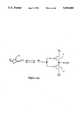
- FIG. 5(a)shows a dual input universal logic structure according to the invention comprising a P-channel and an N-channel FET.
- FIG. 5(b)shows a logic table for the dual input universal logic structure.
- FIG. 6shows a multiplexer circuit which includes the dual input logic structure of FIG. 5.
- FIG. 7shows an exclusive NOR circuit which includes the dual input logic structure of FIG. 5.
- FIG. 8shows a two-by-four decoder circuit which includes the dual input logic structure of FIG. 5.
- FIG. 9shows the dual input logic structure implemented to latch data from an input port to an output port.
- FIG. 10shows the dual input logic structure implemented within a static RAM circuit.
- FIG. 11shows a conventional RAM circuit.
- Dual input structure 100comprises a P-channel field effect transistor (CMOS) 101 and an N-channel field effect transistor (CMOS) 102.
- the source of P-channel FET 101is connected to receive a first supply voltage V dd .
- a first terminal, either the drain or the source, of N-channel FET 102is connected to an input line designated as B for receiving a second voltage.
- the gates of each transistor 101 and 102are connected together at a common node and form an input line designated as A for receiving a third voltage.
- the drain of P-channel FET 101is connected to a remaining second terminal, either the drain or the source, of N-channel FET 102 at a common node which forms an output line (OUT) for supplying a fourth voltage.
- OUToutput line
- the connections of the drain and the source of transistor 102 within dual input logic structure 100may be interchanged. That is, dual input logic structure 100 will operate if the source of transistor 100 is connected to the output line and the drain is connected to input line B, as well as if the drain were connected to the output line and the source to input line B.
- dual input logic structure 100The operation of dual input logic structure 100 is easily analyzed.
- N-channel FET 102When the voltage level at input line A is logic LOW, N-channel FET 102 is turned off and thus does not conduct, while P-channel transistor 101 is turned on. Consequently, the supply voltage V dd is coupled through a low impedance to the output line, causing the output line to go HIGH.
- the output lineWhen the voltage level at input line A is LOW, the output line remains HIGH regardless of the voltage level at input line B.
- the logic table of FIG. 5(b)is representative of the operation of dual input logic structure 100 where "X" is a don't care state and "b" is the value at input line B just prior to input line A switching to a HIGH state.
- the logical equationis given by:
- Dual input logic structure 100explained above may be used as a building block within circuits which implement more complex logical equations.
- dual input logic structure 100may be used as a building block to design a circuit implementing the multiplexing function given by eq. (1).
- dual input logic structure 100may be used as a building block to form an exclusive NOR circuit or a decoder circuit.
- the design of a circuitincludes dual input logic structure 100 for implementing a particular logical function, the resulting electrical circuit is often composed of fewer CMOS transistors than would be required if conventional logic were used.
- FIG. 6is a multiplexer circuit 105 which implements the same function implemented by the circuit of FIG. 2.
- Multiplexer 105comprises dual input logic structure 100 and includes two additional CMOS transistors 106 and 107.
- the logic equation of multiplexer 105is given by:
- Multiplexer circuit 105utilizes only four CMOS transistors to implement the very same function as the multiplexer circuit shown in FIG. 2(b) which requires twelve transistors. As a consequence, less space on a VLSI chip is required to fabricate multiplexer circuit 105 of FIG. 6.
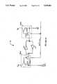
- FIG. 7shows a circuit 110 which implements an exclusive NOR function.
- Exclusive NOR circuit 110includes dual input logic structure 100 and two additional CMOS transistors 111 and 112. The logical function implemented is given by the equation:
- exclusive NOR circuit 110 of FIG. 7requires only four CMOS transistors, while the circuit of FIG. 3(c) which implements the same function requires a total of eight CMOS transistors. Again, use of dual input logic structure 100 results in a circuit requiring fewer CMOS transistors and hence less space in comparison to that required when conventional logic is used.
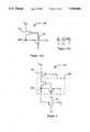
- Decoder circuit 120which implements a two-by-four decoder function.
- Decoder circuit 120 of FIG. 8comprises four of the dual input logic structures 100(a)-(d) and an additional inverter gate 121. Only one output line of decoder 120 is logical LOW at a given time, depending upon the logical levels at input lines A and B.
- Decoder circuit 120 of FIG. 8implements the decoding function using only ten CMOS transistors, in comparison to the circuit of FIG. 4 which, when implemented using conventional logic, requires twenty CMOS transistors.
- Each of the digital circuits as shown in FIGS. 6-8are composed of at least one dual input logic structure 100 and utilize a fewer number of transistors to implement its logical function than would be required if basic logic gates were used. Consequently, the circuits require a smaller area, allowing for a greater number of functions to be implemented within a single VLSI integrated circuit.
- the circuits having dual input logic structure 100may operate quicker than the circuits using standard logic gate circuitry since there is a decrease in the amount of both gate loading and diffusion loading which accordingly decreases the time constants of the circuits.
- Dual input logic structure 100may also be adapted for use within memory circuitry.
- FIG. 9shows dual input logic structure 100 implemented to latch data from an input port (DATA IN) to an output port (DATA OUT).
- a write/read address line (W/R ⁇ AD n )is provided to the gate of each CMOS transistor 101 and 102.
- W/R ⁇ AD nWhen the write/read address line (W/R ⁇ AD n ) is logic LOW, P-channel FET 101 is turned on, and N-channel FET 102 is turned off. Consequently, the output level at the output port terminal goes to logic HIGH due to the source voltage V dd .
- the voltage level at the write/read address lineis logic HIGH, P-channel transistor 101 is off and N-channel transistor 102 is turned on.
- the data at the input portis allowed to propagate to the output port.
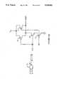
- FIG. 10shows two dual input logic structures 100(a) and 100(b) implemented within a static RAM (random access memory) circuit 130.
- Memory circuit 130also includes two inverters 131 and 132. When the level of the write/read address line (W/R ⁇ AD n ) is logic LOW, memory circuit 130 is in a READ mode and a stored data value is available at the bit lines B/L and B/L since P-channel transistors 101(a) and 101(b) act as resistors with very high L/W values where L is channel length and W is channel width and since diffusion capacitance retains charge on the bit lines. Since P-channel transistors 101(a) and 101(b) act as active pull-ups, they do not affect the charge on the bit lines.
- the memoryWhen the level of the write/read address line goes to logic HIGH, the memory enters a WRITE mode. In the WRITE mode, data on the bit line (B/L) propagates through N-channel transistor 102(a) to node X. Similarly, the complement of the data on the bit line B/L propagates through N-channel transistor 102(b) to node Y. When the write/read address line returns LOW, the data on the bit line terminal is stored at node X, and its complement is stored at node Y. The data is retained at the B/L and B/L lines due to pull-up transistors 101(a) and 101(b) and the diffusion capacitance. A sense amplifier may consequently read the data on the bit lines.
- Static RAM circuit 130 as implemented in FIG. 10has a faster access time and a faster cycle time than the conventional RAM circuit 140 shown in FIG. 11 since static RAM 130 includes an active pull-up at the B/L and B/L bit lines when N-channel transistors 102(a) and 102(b) turn off. Furthermore, the conductor connecting the gates of transistors 101(a), 101(b), 102(a) and 102(b) increases the defined area, and therefore increases the storage node capacitance. Therefore, the storage node charge reduces the soft error rate of the RAM since the transistors' states are not as susceptible to voltage spikes.
- a pre-charge nodeis provided at the gates of transistors 101(a), 101(b), 102(a) and 102(b) and no refresh cycle is required.
- the RAM circuitconsumes less power during the WRITE mode since transistors 101(a) and 101(b) turn off.
Landscapes
- Engineering & Computer Science (AREA)
- Physics & Mathematics (AREA)
- Computer Hardware Design (AREA)
- Computing Systems (AREA)
- General Engineering & Computer Science (AREA)
- Mathematical Physics (AREA)
- Power Engineering (AREA)
- Logic Circuits (AREA)
Abstract
Description
1. Field of the Invention
The invention relates generally to a universal logic structure and more particularly to a dual input universal logic structure for implementing VLSI logic and memory.
2. Description of the Relevant Art
The design of digital circuitry to implement a logical function has primarily involved interconnecting basic logic elements such as AND, OR, NAND, NOR, and inverter gates. After a designer has determined the logical equation to be implemented by circuitry, the basic logic gates may be interconnected in a straight-forward approach to implement the logical function. The number of gates required is usually dependent upon the number of terms and the form of the logical equation to be implemented. It is usually desirable to minimize the number of logical elements used, and there are many techniques which allow a designer to reduce the logical equation in order that the number of gates required may be minimized.
The term "logic design" refers to the process of specifying an interconnection of logic elements in digital computer hardware so that a desired function is performed. Examples of this process might be the design of a circuit that accepts data representing numbers in a gray code and converts this data into a binary-coded decimal representation, or the design of a multiplexer circuit that provides input data from one of two input lines to an output line depending upon the value of a control line. Both formal and ad hoc techniques are used to achieve the desired design.
The basic logic gates are the smallest building blocks that can be represented by operators in an appropriate system of symbolic logic. All digital logic networks in current use operate on signals that are restricted to two possible values only, and are thus called binary values. Table 1(a)-(e) lists each possible combination of binary signals at the inputs of the basic logic gates and the corresponding combination of desired output signals.
TABLE 1(a)-1(e) ______________________________________ Inputs Output ______________________________________ (a)Inverter 0 1 1 0 (b) ANDgate 0 0 0 0 1 0 1 0 0 1 1 1 (c) ORgate 0 0 0 0 1 1 1 0 1 1 1 1 (d) NANDgate 0 0 1 0 1 1 1 0 1 1 1 0 (e)NOR gate 0 0 1 0 1 0 1 0 0 1 1 0 ______________________________________
Each of the basic logic gates is internally composed of electronic components interconnected to perform the associated logical function, typically including a number of CMOS transistors. FIGS. 1(a)-(e) show typical internal circuitry within each of the corresponding basic logic gates. As shown in FIG. 1(a), aNOT gate 10 comprises twoCMOS transistors input NAND gate 13 comprises four CMOS transistors 14-17 as shown in FIG. 1(b). Similarly, a two-input NOR gate 20 shown in FIG. 1(c) comprises four CMOS transistors 21-24. As shown in FIG. 1(d), a two-input ANDgate 25 comprises six CMOS transistors 26-31. Finally, as shown in FIG. 1(e), a two-input OR gate 32 comprises six CMOS transistors 33-38. Although there are circuit configurations other than those shown in FIGS. 1(a)-1(e) which may be designed to implement the logical functions represented by Tables 1(a)-1(e), the circuit configurations as shown represent the simplest forms which require the fewest number of transistors to implement the associated logical functions.
FIG. 2(a) shows a logic diagram of amultiplexer 40 designed using the basic logic gates.Multiplexer 40 includesinverter gates gates gate 45. If conventional logic were used to constructmultiplexer 40, the resulting overall internal circuit configuration would be as shown in FIG. 2(b). The logic equation implemented bymultiplexer 40 is:
OUT=A.sub.1 ·B.sub.1 +A.sub.2 ·B.sub.2 eq. ( 1)
As shown in FIG. 2(b), whenmultiplexer 40 is designed using conventional logic, the resulting overall internal circuit consists of a total of twelve CMOS transistors 46-57.
FIG. 3(a) is a logic circuit of an exclusive NORgate 60 implemented using conventional logic. Exclusive NORgate 60 consists of twoinverters CMOS transistors gate 60 internally consists of eight CMOS transistors 67-74 as shown in FIG. 3(c).
FIG. 4 shows a logical circuit which implements a decoder function. A two-input, four-output decoder 75 shown comprises twoinverter gates
In VLSI (very large scale integration) circuitry, a large number (i.e., over ten thousand) of the basic logical gates may be fabricated on a single integrated circuit chip. The number of basic logic gates used dictate the number of actual FETs which are fabricated on the integrated circuit chip, and consequently determine the size requirements of the chip. It is desirable to decrease the size requirements of VLSI chips and to minimize the number of CMOS transistors used to implement a given logical equation. In addition, it is further desirable to increase the speed at which VLSI circuitry may operate.
A dual input universal logic structure allows many logical functions to be implemented using a relatively small number of CMOS transistors. The dual input structure implements the following logical equation:
OUT=A+B eq. (2)
or
OUT=A·B eq. (3)
The dual input structure consists of two CMOS transistors. When the dual input structure is used in a circuit design, it is often the case that a fewer overall number of CMOS transistors are required than would be required if basic logic gates were used.
The dual input structure may be used to implement a multiplexer or an exclusive NOR function which each require only four CMOS transistors. Likewise, a two-by-four decoder may be implemented using only ten CMOS transistors. Since a fewer number of CMOS transistors are required to implement certain functions, the space requirements of the circuits are reduced. Furthermore, since both gate and diffusion loading are decreased, the circuits may operate faster.
The dual input universal logic structure comprises a P-channel field-effect transistor (FET) and an N-channel field-effect transistor. The source of the P-channel FET is connected to receive a first supply voltage, and a first terminal of the N-channel FET is connected to a first input line. The gates of each of the FETs are connected to each other at a common node which forms a second input line. The drain of the P-channel FET is connected to a second terminal of the N-channel FET at a common node which forms an output line.
The dual input logic structure may further be used to improve latching and memory circuitry. For example, the dual input logic structure may be used within a random access memory circuit to decrease power consumption and soft error rate.
The invention will be more readily understood by reference to the drawings and the detailed description. As will be appreciated by one skilled in the art, the invention is applicable to a universal logic structure in general, and is not limited to VLSI circuitry.
FIG. 1(a) illustrates the logic symbol of an inverter gate and its corresponding internal circuitry.
FIG. 1(b) illustrates the logic symbol for a NAND gate and its corresponding internal circuitry.
FIG. 1(c) illustrates the logic symbol for a NOR gate and its corresponding internal circuitry.
FIG. 1(d) illustrates the logic symbol for an AND gate and its corresponding internal circuitry.
FIG. 1(e) illustrates the logic symbol for an OR gate and its corresponding internal circuitry.
FIG. 2(a) is a logic diagram of a multiplexer using conventional logic.
FIG. 2(b) shows the internal circuitry within the conventional logic of the multiplexer.
FIG. 3(a) is a logic diagram of an exclusive NOR gate using conventional logic.
FIG. 3(b) illustrates the logic symbol of a transmission gate switch and its corresponding internal circuitry.
FIG. 3(c) shows the internal circuitry of the exclusive NOR gate using conventional logic.
FIG. 4 shows a a two-by-four decoder using conventional logic.
FIG. 5(a) shows a dual input universal logic structure according to the invention comprising a P-channel and an N-channel FET.
FIG. 5(b) shows a logic table for the dual input universal logic structure.
FIG. 6 shows a multiplexer circuit which includes the dual input logic structure of FIG. 5.
FIG. 7 shows an exclusive NOR circuit which includes the dual input logic structure of FIG. 5.
FIG. 8 shows a two-by-four decoder circuit which includes the dual input logic structure of FIG. 5.
FIG. 9 shows the dual input logic structure implemented to latch data from an input port to an output port.
FIG. 10 shows the dual input logic structure implemented within a static RAM circuit.
FIG. 11 shows a conventional RAM circuit.
Referring to FIG. 5(a), a dual inputuniversal logic structure 100 according to the invention is shown.Dual input structure 100 comprises a P-channel field effect transistor (CMOS) 101 and an N-channel field effect transistor (CMOS) 102. The source of P-channel FET 101 is connected to receive a first supply voltage Vdd. A first terminal, either the drain or the source, of N-channel FET 102 is connected to an input line designated as B for receiving a second voltage. The gates of eachtransistor channel FET 101 is connected to a remaining second terminal, either the drain or the source, of N-channel FET 102 at a common node which forms an output line (OUT) for supplying a fourth voltage. It should be noted that the connections of the drain and the source oftransistor 102 within dualinput logic structure 100 may be interchanged. That is, dualinput logic structure 100 will operate if the source oftransistor 100 is connected to the output line and the drain is connected to input line B, as well as if the drain were connected to the output line and the source to input line B.
The operation of dualinput logic structure 100 is easily analyzed. When the voltage level at input line A is logic LOW, N-channel FET 102 is turned off and thus does not conduct, while P-channel transistor 101 is turned on. Consequently, the supply voltage Vdd is coupled through a low impedance to the output line, causing the output line to go HIGH. When the voltage level at input line A is LOW, the output line remains HIGH regardless of the voltage level at input line B.
When the voltage level at input line A is logical HIGH, P-channel transistor 101 is turned off, while N-channel transistor 102 is turned on. As a result, the output line is coupled through a low impedance to input line B, and thus the logical voltage level at the output line is equal to the logical level at input line B.
The logic table of FIG. 5(b) is representative of the operation of dualinput logic structure 100 where "X" is a don't care state and "b" is the value at input line B just prior to input line A switching to a HIGH state. The logical equation is given by:
OUT=A+B eq. (2)
or
OUT=A·B eq. (3)
Dualinput logic structure 100 explained above may be used as a building block within circuits which implement more complex logical equations. For example, dualinput logic structure 100 may be used as a building block to design a circuit implementing the multiplexing function given by eq. (1). Similarly, dualinput logic structure 100 may be used as a building block to form an exclusive NOR circuit or a decoder circuit. When the design of a circuit includes dualinput logic structure 100 for implementing a particular logical function, the resulting electrical circuit is often composed of fewer CMOS transistors than would be required if conventional logic were used.
FIG. 6 is amultiplexer circuit 105 which implements the same function implemented by the circuit of FIG. 2.Multiplexer 105 comprises dualinput logic structure 100 and includes twoadditional CMOS transistors multiplexer 105 is given by:
OUT=A.sub.1 ·B.sub.1 +A.sub.2 ·B.sub.2 eq. (4)
FIG. 7 shows acircuit 110 which implements an exclusive NOR function. Exclusive NORcircuit 110 includes dualinput logic structure 100 and twoadditional CMOS transistors
OUT=A·B+B·A eq. (5)
The exclusive NOR function as implemented by exclusive NORcircuit 110 of FIG. 7 requires only four CMOS transistors, while the circuit of FIG. 3(c) which implements the same function requires a total of eight CMOS transistors. Again, use of dualinput logic structure 100 results in a circuit requiring fewer CMOS transistors and hence less space in comparison to that required when conventional logic is used.
Referring next to FIG. 8, adecoder circuit 120 is shown which implements a two-by-four decoder function.Decoder circuit 120 of FIG. 8 comprises four of the dual input logic structures 100(a)-(d) and anadditional inverter gate 121. Only one output line ofdecoder 120 is logical LOW at a given time, depending upon the logical levels at input lines A andB. Decoder circuit 120 of FIG. 8 implements the decoding function using only ten CMOS transistors, in comparison to the circuit of FIG. 4 which, when implemented using conventional logic, requires twenty CMOS transistors.
Each of the digital circuits as shown in FIGS. 6-8 are composed of at least one dualinput logic structure 100 and utilize a fewer number of transistors to implement its logical function than would be required if basic logic gates were used. Consequently, the circuits require a smaller area, allowing for a greater number of functions to be implemented within a single VLSI integrated circuit. In addition, the circuits having dualinput logic structure 100 may operate quicker than the circuits using standard logic gate circuitry since there is a decrease in the amount of both gate loading and diffusion loading which accordingly decreases the time constants of the circuits.
Dualinput logic structure 100 may also be adapted for use within memory circuitry. FIG. 9 shows dualinput logic structure 100 implemented to latch data from an input port (DATA IN) to an output port (DATA OUT). A write/read address line (W/R·ADn) is provided to the gate of eachCMOS transistor channel FET 101 is turned on, and N-channel FET 102 is turned off. Consequently, the output level at the output port terminal goes to logic HIGH due to the source voltage Vdd. When the voltage level at the write/read address line is logic HIGH, P-channel transistor 101 is off and N-channel transistor 102 is turned on. Thus, the data at the input port is allowed to propagate to the output port.
FIG. 10 shows two dual input logic structures 100(a) and 100(b) implemented within a static RAM (random access memory)circuit 130.Memory circuit 130 also includes twoinverters memory circuit 130 is in a READ mode and a stored data value is available at the bit lines B/L and B/L since P-channel transistors 101(a) and 101(b) act as resistors with very high L/W values where L is channel length and W is channel width and since diffusion capacitance retains charge on the bit lines. Since P-channel transistors 101(a) and 101(b) act as active pull-ups, they do not affect the charge on the bit lines.
When the level of the write/read address line goes to logic HIGH, the memory enters a WRITE mode. In the WRITE mode, data on the bit line (B/L) propagates through N-channel transistor 102(a) to node X. Similarly, the complement of the data on the bit line B/L propagates through N-channel transistor 102(b) to node Y. When the write/read address line returns LOW, the data on the bit line terminal is stored at node X, and its complement is stored at node Y. The data is retained at the B/L and B/L lines due to pull-up transistors 101(a) and 101(b) and the diffusion capacitance. A sense amplifier may consequently read the data on the bit lines.
The embodiments described above are intended to be exemplary and not limiting. In view of the above disclosure, modifications will be obvious to one of ordinary skill in the art without departing from the scope of the invention.
Claims (4)
1. A multiplexer circuit comprising:
a first N-channel field effect transistor having a first terminal, a second terminal, and a gate; and
a first P-channel field effect transistor having a drain, a gate, and a source, wherein the drain of said first P-channel field effect transistor is connected to the first terminal of said first N-channel field effect transistor whereat an output node is formed for supplying a first voltage, and wherein the gate of said first P-channel field effect transistor is connected to the gate of said first N-channel field effect transistor whereat a first input node is formed for receiving a second voltage, and wherein the second terminal of said first N-channel field effect transistor forms a second input node for receiving a third voltage, and wherein the source of said first P-channel field effect transistor forms a node for receiving a fourth voltage;
a second P-channel field effect transistor having a drain, a gate, and a source, wherein the drain of said second P-channel field effect transistor is connected to the source of said first P-channel field effect transistor, and wherein the source of said second P-channel field effect transistor forms a node for receiving a fifth voltage; and
a second N-channel field effect transistor having a first terminal, a second terminal, and a gate, wherein the first terminal of said second N-channel field effect transistor is connected to the first terminal of said first N-channel field effect transistor and to the drain of said first P-channel field effect transistor, and wherein the gate of said second N-channel field effect transistor and the gate of said second P-channel field effect transistor are connected to form a third input node for receiving a sixth voltage, and wherein the second terminal of said second N-channel field effect transistor forms a fourth input node for receiving a seventh voltage.
2. An exclusive NOR gate comprising:
a first N-channel field effect transistor having a first terminal, a second terminal, and a gate; and
a first P-channel field effect transistor having a drain, a gate, and a source, wherein the drain of said first P-channel field effect transistor is connected to the first terminal of said first N-channel field effect transistor whereat an output node is formed for supplying a first voltage, and wherein the gate of said first P-channel field effect transistor is connected to the gate of said first N-channel field effect transistor whereat a first input node is formed for receiving a second voltage, and wherein the second terminal of said first N-channel field effect transistor forms a second input node for receiving a third voltage, and wherein the source of said first P-channel field effect transistor forms a node for receiving a fourth voltage;
a second N-channel field effect transistor having a first terminal, a second terminal, and a gate, wherein the first terminal of said second N-channel field effect transistor is connected to the gate of said first N-channel field effect transistor, and wherein the second terminal of said second N-channel field effect transistor is connected to the first terminal of said first N-channel field effect transistor and to the drain of said first P-channel field effect transistor; and
a second P-channel field effect transistor having a drain, a gate, and a source, wherein the drain of said second P-channel field effect transistor is connected to the source of said first field effect transistor, and wherein the gate of said second P-channel transistor is connected to the gate of said second N-channel field effect transistor, and wherein the source of said second P-channel field effect transistor forms a node for receiving a fifth voltage.
3. A decoder circuit comprising:
a first P-channel FET having a drain, a gate, and a source, wherein the gate is connected to a first input node; and wherein the source forms a node for receiving a first voltage;
a first N-channel FET having a first terminal, a second terminal, and a gate, wherein the first terminal is connected to a second input node, and wherein the second terminal is connected to the drain of said first P-channel FET and forms a first output node, and wherein the gate is connected to the gate of said first P-channel FET;
a second P-channel FET having a drain, a gate, and a source, wherein the source is connected to said node for receiving said first voltage, and wherein the gate is connected to the first terminal of said first N-channel FET;
a second N-channel FET having a first terminal, a second terminal, and a gate, wherein the gate is connected to the gate of said second P-channel FET, and wherein the first terminal is connected to said first input node, and wherein the second terminal is connected to the drain of said second P-channel FET and forms a second output node;
an inverter having an input line and an output line, the input line connected to said second input node;
a third P-channel FET having a drain, a gate, and a source, wherein the gate is connected to the gate of said first P-channel FET, and wherein the source is connected to said node for receiving said first voltage;
a third N-channel FET having a first terminal, a second terminal, and a gate, wherein the gate is connected to the gate of said third P-channel FET, and wherein the first terminal is connected to the output line of said inverter, and wherein the second terminal is connected to the drain of said third P-channel FET and forms a third output node;
a fourth P-channel FET having a drain, a gate, and a source, wherein the source is connected to said node for receiving said first voltage, and wherein the gate is connected to the output line of said inverter; and
a fourth N-channel FET having a first terminal, a second terminal, and a gate, wherein the gate is connected to the output line of said inverter, and wherein the first terminal is connected to said first input node, and wherein the second terminal is connected to the drain of said fourth P-channel FET and forms a fourth output node.
4. A random access memory circuit comprising:
a first P-channel FET having a drain, a gate, and a source, wherein the source forms a node for receiving a first voltage;
a first N-channel FET having a first terminal, a second terminal, and a gate, wherein the gate of said first N-channel FET is connected to the gate of said first P-channel FET, and wherein the first terminal is connected to the drain of said first P-channel FET and forms a first bit line;
a first inverter having an input line and an output line, wherein the input line is connected to the second terminal of said first N-channel FET;
a second inverter having an input line and an output line, wherein the output line is connected to the second terminal of said first N-channel FET;
a second P-channel FET having a drain, a gate, and a source, wherein the source is connected to said node for receiving a first voltage; and
a second N-channel FET having a first terminal, a second terminal, and a gate, wherein the first terminal is connected to the drain of said second P-channel FET and forms a second bit line, and wherein the gate is connected to the gate of said second P-channel FET, and wherein the second terminal is connected to the output line of said first inverter and to the input line of said second inverter, and wherein the gate of said first N-channel FET is connected to the gate of said second N-channel FET and forms a node for receiving a second voltage.
Priority Applications (1)
| Application Number | Priority Date | Filing Date | Title |
|---|---|---|---|
| US07/482,615US5039883A (en) | 1990-02-21 | 1990-02-21 | Dual input universal logic structure |
Applications Claiming Priority (1)
| Application Number | Priority Date | Filing Date | Title |
|---|---|---|---|
| US07/482,615US5039883A (en) | 1990-02-21 | 1990-02-21 | Dual input universal logic structure |
Publications (1)
| Publication Number | Publication Date |
|---|---|
| US5039883Atrue US5039883A (en) | 1991-08-13 |
Family
ID=23916749
Family Applications (1)
| Application Number | Title | Priority Date | Filing Date |
|---|---|---|---|
| US07/482,615Expired - LifetimeUS5039883A (en) | 1990-02-21 | 1990-02-21 | Dual input universal logic structure |
Country Status (1)
| Country | Link |
|---|---|
| US (1) | US5039883A (en) |
Cited By (26)
| Publication number | Priority date | Publication date | Assignee | Title |
|---|---|---|---|---|
| US5420529A (en)* | 1994-05-19 | 1995-05-30 | Northern Telecom Limited | Current steering switch and hybrid BiCMOS multiplexer with CMOS commutation signal and CML/ECL data signals |
| US5508641A (en)* | 1994-12-20 | 1996-04-16 | International Business Machines Corporation | Integrated circuit chip and pass gate logic family therefor |
| US5539331A (en)* | 1993-05-10 | 1996-07-23 | Kabushiki Kaisha Toshiba | Field programmable gate array having transmission gates and semiconductor integrated circuit for programming connection of wires |
| US6232795B1 (en)* | 1996-01-17 | 2001-05-15 | Nec Corporation | Logic circuit with single charge pulling out transistor and semiconductor integrated circuit using the same |
| US6255855B1 (en)* | 1998-12-22 | 2001-07-03 | Infineon Technologies Ag | Integrated circuit having a decoder |
| US6396896B1 (en) | 2000-04-28 | 2002-05-28 | 3G.Com Inc. | Implementation of functions of multiple successive bits of a shift register |
| NL1020289C2 (en)* | 2002-04-02 | 2003-10-03 | Jan Hendrik Van De Pol | Device for adding or subtracting. |
| US20050083100A1 (en)* | 2003-10-21 | 2005-04-21 | Ching-Wu Tseng | Voltage level shifter |
| CN1320760C (en)* | 2002-09-25 | 2007-06-06 | 株式会社半导体能源研究所 | Clocked Inverters, NAND Gates, NOR Gates, and Shift Registers |
| US20110102018A1 (en)* | 2009-10-30 | 2011-05-05 | Semiconductor Energy Laboratory Co., Ltd. | Logic circuit and semiconductor device |
| US20120280715A1 (en)* | 2011-05-06 | 2012-11-08 | Semiconductor Energy Laboratory Co., Ltd. | Logic circuit and semiconductor device |
| US8471256B2 (en) | 2009-11-27 | 2013-06-25 | Semiconductor Energy Laboratory Co., Ltd. | Semiconductor device and method for manufacturing the same |
| US8630110B2 (en) | 2011-05-06 | 2014-01-14 | Semiconductor Energy Laboratory Co., Ltd. | Semiconductor memory device |
| US8638123B2 (en) | 2011-05-20 | 2014-01-28 | Semiconductor Energy Laboratory Co., Ltd. | Adder including transistor having oxide semiconductor layer |
| US8705292B2 (en) | 2011-05-13 | 2014-04-22 | Semiconductor Energy Laboratory Co., Ltd. | Nonvolatile memory circuit with an oxide semiconductor transistor for reducing power consumption and electronic device |
| US8787084B2 (en) | 2011-03-30 | 2014-07-22 | Semiconductor Energy Laboratory Co., Ltd. | Semiconductor device and driving method thereof |
| US9064574B2 (en) | 2012-11-06 | 2015-06-23 | Semiconductor Energy Laboratory Co., Ltd. | Semiconductor device and driving method thereof |
| US9064596B2 (en) | 2013-02-12 | 2015-06-23 | Semiconductor Energy Laboratory Co., Ltd. | Semiconductor device |
| US9135182B2 (en) | 2012-06-01 | 2015-09-15 | Semiconductor Energy Laboratory Co., Ltd. | Central processing unit and driving method thereof |
| US9225329B2 (en) | 2014-03-07 | 2015-12-29 | Semiconductor Energy Laboratory Co., Ltd. | Semiconductor device, driving method thereof, and electronic appliance |
| US9245589B2 (en) | 2013-03-25 | 2016-01-26 | Semiconductor Energy Laboratory Co., Ltd. | Semiconductor device having Schmitt trigger NAND circuit and Schmitt trigger inverter |
| US9293186B2 (en) | 2013-03-14 | 2016-03-22 | Semiconductor Energy Laboratory Co., Ltd. | Memory device and semiconductor device |
| US9336845B2 (en) | 2011-05-20 | 2016-05-10 | Semiconductor Energy Laboratory Co., Ltd. | Register circuit including a volatile memory and a nonvolatile memory |
| US9385713B2 (en) | 2014-10-10 | 2016-07-05 | Semiconductor Energy Laboratory Co., Ltd. | Logic circuit, processing unit, electronic component, and electronic device |
| US9601215B2 (en) | 2014-04-11 | 2017-03-21 | Semiconductor Energy Laboratory Co., Ltd. | Holding circuit, driving method of the holding circuit, and semiconductor device including the holding circuit |
| US10177142B2 (en) | 2015-12-25 | 2019-01-08 | Semiconductor Energy Laboratory Co., Ltd. | Circuit, logic circuit, processor, electronic component, and electronic device |
Citations (6)
| Publication number | Priority date | Publication date | Assignee | Title |
|---|---|---|---|---|
| US4453096A (en)* | 1976-11-04 | 1984-06-05 | U.S. Philips Corporation | MOS Transistor type integrated circuit for the execution of logical operations on a plurality of data signals |
| US4620117A (en)* | 1985-01-04 | 1986-10-28 | Advanced Micro Devices, Inc. | Balanced CMOS logic circuits |
| US4710649A (en)* | 1986-04-11 | 1987-12-01 | Raytheon Company | Transmission-gate structured logic circuits |
| US4866305A (en)* | 1986-12-19 | 1989-09-12 | Fujitsu Limited | Multiple-input multiple-output decoding circuit |
| US4893031A (en)* | 1987-12-23 | 1990-01-09 | Kabushiki Kaisha Toshiba | Logical circuits for performing logical functions without a power supply |
| US4910417A (en)* | 1986-09-19 | 1990-03-20 | Actel Corporation | Universal logic module comprising multiplexers |
- 1990
- 1990-02-21USUS07/482,615patent/US5039883A/ennot_activeExpired - Lifetime
Patent Citations (6)
| Publication number | Priority date | Publication date | Assignee | Title |
|---|---|---|---|---|
| US4453096A (en)* | 1976-11-04 | 1984-06-05 | U.S. Philips Corporation | MOS Transistor type integrated circuit for the execution of logical operations on a plurality of data signals |
| US4620117A (en)* | 1985-01-04 | 1986-10-28 | Advanced Micro Devices, Inc. | Balanced CMOS logic circuits |
| US4710649A (en)* | 1986-04-11 | 1987-12-01 | Raytheon Company | Transmission-gate structured logic circuits |
| US4910417A (en)* | 1986-09-19 | 1990-03-20 | Actel Corporation | Universal logic module comprising multiplexers |
| US4866305A (en)* | 1986-12-19 | 1989-09-12 | Fujitsu Limited | Multiple-input multiple-output decoding circuit |
| US4893031A (en)* | 1987-12-23 | 1990-01-09 | Kabushiki Kaisha Toshiba | Logical circuits for performing logical functions without a power supply |
Cited By (50)
| Publication number | Priority date | Publication date | Assignee | Title |
|---|---|---|---|---|
| US5539331A (en)* | 1993-05-10 | 1996-07-23 | Kabushiki Kaisha Toshiba | Field programmable gate array having transmission gates and semiconductor integrated circuit for programming connection of wires |
| US5420529A (en)* | 1994-05-19 | 1995-05-30 | Northern Telecom Limited | Current steering switch and hybrid BiCMOS multiplexer with CMOS commutation signal and CML/ECL data signals |
| US5508641A (en)* | 1994-12-20 | 1996-04-16 | International Business Machines Corporation | Integrated circuit chip and pass gate logic family therefor |
| US6232795B1 (en)* | 1996-01-17 | 2001-05-15 | Nec Corporation | Logic circuit with single charge pulling out transistor and semiconductor integrated circuit using the same |
| US6255855B1 (en)* | 1998-12-22 | 2001-07-03 | Infineon Technologies Ag | Integrated circuit having a decoder |
| US6396896B1 (en) | 2000-04-28 | 2002-05-28 | 3G.Com Inc. | Implementation of functions of multiple successive bits of a shift register |
| NL1020289C2 (en)* | 2002-04-02 | 2003-10-03 | Jan Hendrik Van De Pol | Device for adding or subtracting. |
| EP1351393A1 (en)* | 2002-04-02 | 2003-10-08 | Jan Hendrik Van De Pol | Device and method for adding and/or subtracting |
| US20040085095A1 (en)* | 2002-04-02 | 2004-05-06 | Van De Pol Jan Hendrik | Device and method for adding and/or subtracting |
| CN1320760C (en)* | 2002-09-25 | 2007-06-06 | 株式会社半导体能源研究所 | Clocked Inverters, NAND Gates, NOR Gates, and Shift Registers |
| US20050083100A1 (en)* | 2003-10-21 | 2005-04-21 | Ching-Wu Tseng | Voltage level shifter |
| US7071758B2 (en)* | 2003-10-21 | 2006-07-04 | Novatek Microelectronics Corp. | Voltage level shifter |
| US20130002326A1 (en)* | 2009-10-30 | 2013-01-03 | Semiconductor Energy Laboratory Co., Ltd. | Logic circuit and semiconductor device |
| US20110102018A1 (en)* | 2009-10-30 | 2011-05-05 | Semiconductor Energy Laboratory Co., Ltd. | Logic circuit and semiconductor device |
| CN102687400A (en)* | 2009-10-30 | 2012-09-19 | 株式会社半导体能源研究所 | Logic circuit and semiconductor device |
| CN102687400B (en)* | 2009-10-30 | 2016-08-24 | 株式会社半导体能源研究所 | Logic circuit and semiconductor device |
| US9722086B2 (en) | 2009-10-30 | 2017-08-01 | Semiconductor Energy Laboratory Co., Ltd. | Logic circuit and semiconductor device |
| US8207756B2 (en)* | 2009-10-30 | 2012-06-26 | Semiconductor Energy Laboratory Co., Ltd. | Logic circuit and semiconductor device |
| US8570070B2 (en)* | 2009-10-30 | 2013-10-29 | Semiconductor Energy Laboratory Co., Ltd. | Logic circuit and semiconductor device |
| US8471256B2 (en) | 2009-11-27 | 2013-06-25 | Semiconductor Energy Laboratory Co., Ltd. | Semiconductor device and method for manufacturing the same |
| US12396292B2 (en) | 2009-11-27 | 2025-08-19 | Semiconductor Energy Laboratory Co., Ltd. | Semiconductor device comprising first and second conductive layers |
| US9748436B2 (en) | 2009-11-27 | 2017-08-29 | Semiconductor Energy Laboratory Co., Ltd. | Semiconductor device and method for manufacturing the same |
| US11894486B2 (en) | 2009-11-27 | 2024-02-06 | Semiconductor Energy Laboratory Co., Ltd. | Method for manufacturing semiconductor device |
| US10396236B2 (en) | 2009-11-27 | 2019-08-27 | Semiconductor Energy Laboratory Co., Ltd. | Semiconductor device and display device |
| US20190109259A1 (en) | 2009-11-27 | 2019-04-11 | Semiconductor Energy Laboratory Co., Ltd. | Semiconductor device and method for manufacturing the same |
| US8787084B2 (en) | 2011-03-30 | 2014-07-22 | Semiconductor Energy Laboratory Co., Ltd. | Semiconductor device and driving method thereof |
| US9076520B2 (en) | 2011-03-30 | 2015-07-07 | Semiconductor Energy Laboratory Co., Ltd. | Semiconductor device and driving method thereof |
| US8630110B2 (en) | 2011-05-06 | 2014-01-14 | Semiconductor Energy Laboratory Co., Ltd. | Semiconductor memory device |
| US9444459B2 (en)* | 2011-05-06 | 2016-09-13 | Semiconductor Energy Laboratory Co., Ltd. | Logic circuit and semiconductor device |
| US20120280715A1 (en)* | 2011-05-06 | 2012-11-08 | Semiconductor Energy Laboratory Co., Ltd. | Logic circuit and semiconductor device |
| US8705292B2 (en) | 2011-05-13 | 2014-04-22 | Semiconductor Energy Laboratory Co., Ltd. | Nonvolatile memory circuit with an oxide semiconductor transistor for reducing power consumption and electronic device |
| US9336845B2 (en) | 2011-05-20 | 2016-05-10 | Semiconductor Energy Laboratory Co., Ltd. | Register circuit including a volatile memory and a nonvolatile memory |
| US9122896B2 (en) | 2011-05-20 | 2015-09-01 | Semiconductor Energy Laboratory Co., Ltd. | Adder |
| US8638123B2 (en) | 2011-05-20 | 2014-01-28 | Semiconductor Energy Laboratory Co., Ltd. | Adder including transistor having oxide semiconductor layer |
| US9135182B2 (en) | 2012-06-01 | 2015-09-15 | Semiconductor Energy Laboratory Co., Ltd. | Central processing unit and driving method thereof |
| US9064574B2 (en) | 2012-11-06 | 2015-06-23 | Semiconductor Energy Laboratory Co., Ltd. | Semiconductor device and driving method thereof |
| US9064596B2 (en) | 2013-02-12 | 2015-06-23 | Semiconductor Energy Laboratory Co., Ltd. | Semiconductor device |
| US9293186B2 (en) | 2013-03-14 | 2016-03-22 | Semiconductor Energy Laboratory Co., Ltd. | Memory device and semiconductor device |
| US9536592B2 (en) | 2013-03-14 | 2017-01-03 | Semiconductor Energy Laboratory Co., Ltd. | Memory device and semiconductor device |
| US9245589B2 (en) | 2013-03-25 | 2016-01-26 | Semiconductor Energy Laboratory Co., Ltd. | Semiconductor device having Schmitt trigger NAND circuit and Schmitt trigger inverter |
| US9225329B2 (en) | 2014-03-07 | 2015-12-29 | Semiconductor Energy Laboratory Co., Ltd. | Semiconductor device, driving method thereof, and electronic appliance |
| US9601215B2 (en) | 2014-04-11 | 2017-03-21 | Semiconductor Energy Laboratory Co., Ltd. | Holding circuit, driving method of the holding circuit, and semiconductor device including the holding circuit |
| US9385713B2 (en) | 2014-10-10 | 2016-07-05 | Semiconductor Energy Laboratory Co., Ltd. | Logic circuit, processing unit, electronic component, and electronic device |
| US10453863B2 (en) | 2014-10-10 | 2019-10-22 | Semiconductor Energy Laboratory Co., Ltd. | Logic circuit, processing unit, electronic component, and electronic device |
| US10825836B2 (en) | 2014-10-10 | 2020-11-03 | Semiconductor Energy Laboratory Co., Ltd. | Logic circuit, processing unit, electronic component, and electronic device |
| US11374023B2 (en) | 2014-10-10 | 2022-06-28 | Semiconductor Energy Laboratory Co., Ltd. | Logic circuit, processing unit, electronic component, and electronic device |
| US10153301B2 (en) | 2014-10-10 | 2018-12-11 | Semiconductor Energy Laboratory Co., Ltd. | Logic circuit, processing unit, electronic component, and electronic device |
| US12057451B2 (en) | 2014-10-10 | 2024-08-06 | Semiconductor Energy Laboratory Co., Ltd. | Logic circuit, processing unit, electronic component, and electronic device |
| US9704882B2 (en) | 2014-10-10 | 2017-07-11 | Semiconductor Energy Laboratory Co., Ltd. | Logic circuit, processing unit, electronic component, and electronic device |
| US10177142B2 (en) | 2015-12-25 | 2019-01-08 | Semiconductor Energy Laboratory Co., Ltd. | Circuit, logic circuit, processor, electronic component, and electronic device |
Similar Documents
| Publication | Publication Date | Title |
|---|---|---|
| US5039883A (en) | Dual input universal logic structure | |
| US4710649A (en) | Transmission-gate structured logic circuits | |
| US5777491A (en) | High-performance differential cascode voltage switch with pass gate logic elements | |
| US6066965A (en) | Method and apparatus for a N-nary logic circuit using 1 of 4 signals | |
| US6111425A (en) | Very low power logic circuit family with enhanced noise immunity | |
| US6476644B2 (en) | Clocked logic gate circuit | |
| US6069497A (en) | Method and apparatus for a N-nary logic circuit using 1 of N signals | |
| US4713790A (en) | Exclusive OR/NOR gate having cross-coupled transistors | |
| US4749886A (en) | Reduced parallel EXCLUSIVE or and EXCLUSIVE NOR gate | |
| US5095230A (en) | Data output circuit of semiconductor device | |
| US5568069A (en) | High speed, low power pipelined logic circuit | |
| US6975151B2 (en) | Latch circuit having reduced input/output load memory and semiconductor chip | |
| US6707318B2 (en) | Low power entry latch to interface static logic with dynamic logic | |
| EP0342592B1 (en) | Chip enable input circuit in semiconductor memory device | |
| US5831458A (en) | Output circuit having BiNMOS inverters | |
| US5332936A (en) | Composite logic circuit | |
| US7098704B2 (en) | Semiconductor integrated circuit device | |
| US5532634A (en) | High-integration J-K flip-flop circuit | |
| US4587665A (en) | Binary counter having buffer and coincidence circuits for the switched bistable stages thereof | |
| US5748541A (en) | Latch circuit operating in synchronization with clock signals | |
| US6339347B1 (en) | Method and apparatus for ratioed logic structure that uses zero or negative threshold voltage | |
| US20020036912A1 (en) | Content addressable memory (CAM) for data lookups in a data processing system | |
| US6911846B1 (en) | Method and apparatus for a 1 of N signal | |
| Wang et al. | A high-speed single-phase-clocked CMOS priority encoder | |
| JPS6125321A (en) | Data latch circuit |
Legal Events
| Date | Code | Title | Description |
|---|---|---|---|
| AS | Assignment | Owner name:NEC ELECTRONIC INC., A CORP. OF CA, CALIFORNIA Free format text:ASSIGNMENT OF ASSIGNORS INTEREST.;ASSIGNOR:ON, KEVIN;REEL/FRAME:005235/0873 Effective date:19900221 | |
| STCF | Information on status: patent grant | Free format text:PATENTED CASE | |
| FPAY | Fee payment | Year of fee payment:4 | |
| FPAY | Fee payment | Year of fee payment:8 | |
| FPAY | Fee payment | Year of fee payment:12 | |
| REMI | Maintenance fee reminder mailed | ||
| AS | Assignment | Owner name:NEC ELECTRONICS AMERICA, INC., CALIFORNIA Free format text:CHANGE OF NAME OF ASSIGNEE;ASSIGNOR:NEC ELECTRONICS, INC.;REEL/FRAME:026110/0316 Effective date:20020924 | |
| AS | Assignment | Owner name:RENESAS ELECTRONICS AMERICA, INC., CALIFORNIA Free format text:MERGER;ASSIGNOR:NEC ELECTRONICS AMERICA, INC.;REEL/FRAME:026110/0643 Effective date:20100401 |