US5039548A - Plasma chemical vapor reaction method employing cyclotron resonance - Google Patents
Plasma chemical vapor reaction method employing cyclotron resonanceDownload PDFInfo
- Publication number
- US5039548A US5039548AUS07/299,014US29901489AUS5039548AUS 5039548 AUS5039548 AUS 5039548AUS 29901489 AUS29901489 AUS 29901489AUS 5039548 AUS5039548 AUS 5039548A
- Authority
- US
- United States
- Prior art keywords
- substrate
- plasma
- magnetic field
- reaction chamber
- gas
- Prior art date
- Legal status (The legal status is an assumption and is not a legal conclusion. Google has not performed a legal analysis and makes no representation as to the accuracy of the status listed.)
- Expired - Lifetime
Links
Images


Classifications
- H—ELECTRICITY
- H01—ELECTRIC ELEMENTS
- H01J—ELECTRIC DISCHARGE TUBES OR DISCHARGE LAMPS
- H01J37/00—Discharge tubes with provision for introducing objects or material to be exposed to the discharge, e.g. for the purpose of examination or processing thereof
- H01J37/32—Gas-filled discharge tubes
- H01J37/32009—Arrangements for generation of plasma specially adapted for examination or treatment of objects, e.g. plasma sources
- H01J37/32192—Microwave generated discharge
- C—CHEMISTRY; METALLURGY
- C23—COATING METALLIC MATERIAL; COATING MATERIAL WITH METALLIC MATERIAL; CHEMICAL SURFACE TREATMENT; DIFFUSION TREATMENT OF METALLIC MATERIAL; COATING BY VACUUM EVAPORATION, BY SPUTTERING, BY ION IMPLANTATION OR BY CHEMICAL VAPOUR DEPOSITION, IN GENERAL; INHIBITING CORROSION OF METALLIC MATERIAL OR INCRUSTATION IN GENERAL
- C23C—COATING METALLIC MATERIAL; COATING MATERIAL WITH METALLIC MATERIAL; SURFACE TREATMENT OF METALLIC MATERIAL BY DIFFUSION INTO THE SURFACE, BY CHEMICAL CONVERSION OR SUBSTITUTION; COATING BY VACUUM EVAPORATION, BY SPUTTERING, BY ION IMPLANTATION OR BY CHEMICAL VAPOUR DEPOSITION, IN GENERAL
- C23C16/00—Chemical coating by decomposition of gaseous compounds, without leaving reaction products of surface material in the coating, i.e. chemical vapour deposition [CVD] processes
- C23C16/44—Chemical coating by decomposition of gaseous compounds, without leaving reaction products of surface material in the coating, i.e. chemical vapour deposition [CVD] processes characterised by the method of coating
- C23C16/50—Chemical coating by decomposition of gaseous compounds, without leaving reaction products of surface material in the coating, i.e. chemical vapour deposition [CVD] processes characterised by the method of coating using electric discharges
- C23C16/511—Chemical coating by decomposition of gaseous compounds, without leaving reaction products of surface material in the coating, i.e. chemical vapour deposition [CVD] processes characterised by the method of coating using electric discharges using microwave discharges
- H—ELECTRICITY
- H01—ELECTRIC ELEMENTS
- H01J—ELECTRIC DISCHARGE TUBES OR DISCHARGE LAMPS
- H01J37/00—Discharge tubes with provision for introducing objects or material to be exposed to the discharge, e.g. for the purpose of examination or processing thereof
- H01J37/32—Gas-filled discharge tubes
- H01J37/32009—Arrangements for generation of plasma specially adapted for examination or treatment of objects, e.g. plasma sources
- H01J37/32357—Generation remote from the workpiece, e.g. down-stream
- H—ELECTRICITY
- H01—ELECTRIC ELEMENTS
- H01J—ELECTRIC DISCHARGE TUBES OR DISCHARGE LAMPS
- H01J37/00—Discharge tubes with provision for introducing objects or material to be exposed to the discharge, e.g. for the purpose of examination or processing thereof
- H01J37/32—Gas-filled discharge tubes
- H01J37/32431—Constructional details of the reactor
- H01J37/32623—Mechanical discharge control means
- H—ELECTRICITY
- H01—ELECTRIC ELEMENTS
- H01J—ELECTRIC DISCHARGE TUBES OR DISCHARGE LAMPS
- H01J37/00—Discharge tubes with provision for introducing objects or material to be exposed to the discharge, e.g. for the purpose of examination or processing thereof
- H01J37/32—Gas-filled discharge tubes
- H01J37/32431—Constructional details of the reactor
- H01J37/3266—Magnetic control means
Definitions
- the present inventionrelates to a plasma chemical vapor reaction apparatus, and particularly, though not exclusively, relates to a plasma ECR CVD.
- the ECR CVDhas attracted the interest of researchers due to its high rate excitation ability.
- This deposition methodmakes use of ECR (Electron Cyclotron Resonance) which takes place between charged particles and microwaves in a magnetic field. Since the energy induced by ECR is very high, a substrate to be treated tends to suffer from sputtering damage. Substrates have been therefore located apart from the position in which ECR conditions of the magnetic field and the microwaves are satisfied.
- the pressure of the reactive gaswas on the order of 10 -4 Torr in order to enable the excited gas to reach the substrate to be processed, and high crystallized deposition, such as diamond, can not be formed.
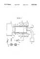
- FIG. 1is a schematic view showing a plasma CVD apparatus in accordance with the present invention.
- FIGS. 2(A) and 2(B)are cross sectional and plan views showing Ioffe bars comprising electromagnetics.
- FIGS. 3(A) and 3(B)are cross sectional and plan views showing Ioffe bars comprising permanent magnets.
- FIG. 4is a cross sectional view showing a modification of the Ioffe bars illustrated in FIGS. 3(A) and 3(B)
- FIG. 5is a schematic illustration showing the magnetic field strength profile in a plasma generating space in accordance with a prior art ECR CVD apparatus.
- FIG. 6is a schematic illustration showing the magnetic field strength in a plasma generating space in accordance with the present invention.
- FIG. 7is an explanatory view showing the drift forces excerted on plasma in accordance wit the present invention.
- the apparatuscomprises a reaction chamber in which a plasma generating space 1 and an auxiliary space 8 are defined which can be maintained at an appropriate negative pressure by means of an evacuating system 9.
- Gas introduction system 11 and 10are connected to the plasma generating space 1 and the auxiliary space 8 respectively.
- Microwavesare introduced into the plasma generating space 1 from a microwave generator 1 through a wave guide 7.
- Helmhortz coils 5 and Ioffe bars 6are located surrounding the plasma generating space 1.
- the Ioffe bars 6are arranged along the microwave propagation direction and depicted in FIGS. 2(A) and 2(B) in case constructed with electromagnets and FIGS.
- FIGS. 3(A) and 3(B)in case with permanent magnets.
- arrowsindicate the magnetic moments of the permanent magnets.
- FIG. 4shows a modification of the Ioffe bars illustrated in FIGS. 3(A) and 3(B).
- a substrate 2 to be treatedis mounted on a substrate holder 3 which is adapted to heat the substrate 2.
- the substrate holder 3is made of a ceramic, e.g. aluminum nitride, which less disturbs the magnetic field induced by the magnets 5 and 6.
- FIG. 5shows the configuration of a conventional location.
- a number of curveshave been drafted within the plasma generating space 1 to trace equi-strength surfaces of the magnetic field induced by the magnets 5 and 6.
- the magnetic fieldbecomes stronger as the site departs from the center of the substrate 2.
- plasmaexperiences drift forces toward the weaker position, i.e. the direction leaving from the substrate 2. Namely, there is a tendency to gather plasma about the generating space 1 rather than the substrate surface to be processed.
- the drift force exerted on plasma in a magnetic fieldis in proportion to -grad B, where B is the absolute strength of the magnetic field.
- the equi-strength surfaces in case of the present inventionare shown in FIG. 6.
- the magnetic fieldbecomes stronger at a nearer position to the substrate 2.
- the drifting force exerted on plasmais shown in FIG. 7 by arrows.
- the arrow 12represents the drift force for drifting plasma toward the substrate 2 mainly induced by the Helmholtz coils 5.
- the arrows 13represents a centripetal force which is induced mainly by the Ioffe bars 6.
- the electron beam diffraction image of the thin carbon films deposited in accordance with the present inventionwas taken.
- spot patterns indicative of the existence of diamond structurewere observed together with halo patterns which are peculier to amorphous structure.
- the carbon filmswere made of i-carbon.
- i-carbon (diamond like carbon) filmscan be formed when the substrate is not heated.
- the diamond like carbonis an amorphous carbon, but has a high abrasion-proof surface and a high thermal conductivity.
- the halo patternsgradually disappeared and, at not lower than 650° C., the thin films were confirmed to be diamond films.
- the Raman spectrum of the filmhad a blunt peak about 1500 cm -1 and a sharp peak about 1333 cm -1 which indicates the existence of diamond.
- Improved silicon carbide films and aluminum nitride filmscan be formed in accordance with the present invention using methyl silane and gaseous aluminum compound and ammonia respectively. Also, tungsten, titanuim, molibdenum or their silicates having high melting points can be formed in the same manner.
- the crystallinity of films in accordance with the present inventioncould be increased by adding water or oxygen into the reactive gas.
- the specific embodimentis explained concerning deposition, the present invention is applicable to general plasma processes in a magnetic field, such as plasma etching process and plasma cleaning process.
- a UV light sourcemay be provided for exposing the reactive gas in the chamber in order to ensure the excited state of the reaction gas near the substrate to be processed.
- a DC bias voltagemay be applied to the reaction gas in plasma state.
- the biascan be applied by means of a voltage supply 14 connected between the substrate holder 3 and an electrode mesh 15 as illustrated if FIG. 1.
- the bias voltageis applied with the holder 3 being the cathode in case of Si deposition, and with the mesh 15 being the cathode in case of carbon deposition or etching using F - or B - .
- the bias voltageIn case of the holder made from a conductive material, the bias voltage consists only of a DC component. In case of the holder made from a non-conductive material, the bias voltage consists of a DC component and a superimposed AC component.
Landscapes
- Chemical & Material Sciences (AREA)
- Engineering & Computer Science (AREA)
- Physics & Mathematics (AREA)
- Plasma & Fusion (AREA)
- Analytical Chemistry (AREA)
- General Chemical & Material Sciences (AREA)
- Chemical Kinetics & Catalysis (AREA)
- Materials Engineering (AREA)
- Mechanical Engineering (AREA)
- Metallurgy (AREA)
- Organic Chemistry (AREA)
- Chemical Vapour Deposition (AREA)
Abstract
Description
The present invention relates to a plasma chemical vapor reaction apparatus, and particularly, though not exclusively, relates to a plasma ECR CVD.
The ECR CVD has attracted the interest of researchers due to its high rate excitation ability. This deposition method makes use of ECR (Electron Cyclotron Resonance) which takes place between charged particles and microwaves in a magnetic field. Since the energy induced by ECR is very high, a substrate to be treated tends to suffer from sputtering damage. Substrates have been therefore located apart from the position in which ECR conditions of the magnetic field and the microwaves are satisfied.
However, in the prior art ECR CVD technique, the pressure of the reactive gas was on the order of 10-4 Torr in order to enable the excited gas to reach the substrate to be processed, and high crystallized deposition, such as diamond, can not be formed.
It is an object of the present invention to provide a plasma chemical vapor reaction apparatus capable of effective treatment of a substrate.
It is another object of the present invention to provide a plasma chemical vapor reaction apparatus capable of depositing highly crystallized films on substrates.
FIG. 1 is a schematic view showing a plasma CVD apparatus in accordance with the present invention.
FIGS. 2(A) and 2(B) are cross sectional and plan views showing Ioffe bars comprising electromagnetics.
FIGS. 3(A) and 3(B) are cross sectional and plan views showing Ioffe bars comprising permanent magnets.
FIG. 4 is a cross sectional view showing a modification of the Ioffe bars illustrated in FIGS. 3(A) and 3(B)
FIG. 5 is a schematic illustration showing the magnetic field strength profile in a plasma generating space in accordance with a prior art ECR CVD apparatus.
FIG. 6 is a schematic illustration showing the magnetic field strength in a plasma generating space in accordance with the present invention.
FIG. 7 is an explanatory view showing the drift forces excerted on plasma in accordance wit the present invention.
Referring now to FIG. 1, an exemplary microwave enhanced plasma CVD apparatus in accordance with the present invention is illustrated. The apparatus comprises a reaction chamber in which aplasma generating space 1 and anauxiliary space 8 are defined which can be maintained at an appropriate negative pressure by means of an evacuatingsystem 9.Gas introduction system plasma generating space 1 and theauxiliary space 8 respectively. Microwaves are introduced into theplasma generating space 1 from amicrowave generator 1 through awave guide 7. Helmhortzcoils 5 and Ioffebars 6 are located surrounding theplasma generating space 1. The Ioffebars 6 are arranged along the microwave propagation direction and depicted in FIGS. 2(A) and 2(B) in case constructed with electromagnets and FIGS. 3(A) and 3(B) in case with permanent magnets. In FIGS. 3(A) and 3(B), arrows indicate the magnetic moments of the permanent magnets. FIG. 4 shows a modification of the Ioffe bars illustrated in FIGS. 3(A) and 3(B). Asubstrate 2 to be treated is mounted on asubstrate holder 3 which is adapted to heat thesubstrate 2. Thesubstrate holder 3 is made of a ceramic, e.g. aluminum nitride, which less disturbs the magnetic field induced by themagnets
The relative location of thesubstrate 2 with respect to the Helmholtzcoils 5 is very important. FIG. 5 shows the configuration of a conventional location. A number of curves have been drafted within theplasma generating space 1 to trace equi-strength surfaces of the magnetic field induced by themagnets substrate 2. In this configuration, plasma experiences drift forces toward the weaker position, i.e. the direction leaving from thesubstrate 2. Namely, there is a tendency to gather plasma about the generatingspace 1 rather than the substrate surface to be processed. Generally speaking, the drift force exerted on plasma in a magnetic field is in proportion to -grad B, where B is the absolute strength of the magnetic field. The equi-strength surfaces in case of the present invention are shown in FIG. 6. The magnetic field becomes stronger at a nearer position to thesubstrate 2. The drifting force exerted on plasma is shown in FIG. 7 by arrows. Thearrow 12 represents the drift force for drifting plasma toward thesubstrate 2 mainly induced by the Helmholtzcoils 5. Thearrows 13 represents a centripetal force which is induced mainly by the Ioffebars 6.
Next, an exemplary method for depositing carbon films on a substrate by use of this apparatus is described. After evacuating the chamber by means of the evacuatingsystem 9, hydrogen is admitted to theplasma generating space 1 at 10SCCM from thegas feeding system 11. The Helmholtzcoils 5 are energized in order to induce a 2K Gauss magnetic field in theplasma generating space 1. The Ioffebars 6 modify the magnetic field to produce a centripetal drift force. 2.45 GHz microwaves are inputted from themicrowave generator 4 at 500 W. By virtue of resonance between the microwaves and hydrogen atoms and electrons, excited hydrogen ions and electrons are produced. The resonance may take place in an ECR mode, a MCR (Mixed Cyclotron Resonance) mode or the whistler mode. The pressure of hydrogen is maintained at 0.1 Pa. Hence, high hydrogen atoms or electrons collide with the surface of thesubstrate 2 and perform plasma cleaning.
After cleaning the substrate surface, the introduction of hydrogen is stopped and a carbon compound gas such as CH4, C2 H4, C2 H2, CH3 OH and C2 H5 OH is introduced instead. The carbon compound gas is excited in the same manner as the hydrogen cleaning and deposits a carbon thin film of diamond or an i-carbon. In accordance with experiments, diamond films could be formed when the substrate temperature was not lower than 450° C. When the deposition was carried out in the same manner but without a magnetic field, only graphite films was formed.
the electron beam diffraction image of the thin carbon films deposited in accordance with the present invention was taken. In the image, spot patterns indicative of the existence of diamond structure were observed together with halo patterns which are peculier to amorphous structure. This means that the carbon films were made of i-carbon. It was confirmed that i-carbon (diamond like carbon) films can be formed when the substrate is not heated. The diamond like carbon is an amorphous carbon, but has a high abrasion-proof surface and a high thermal conductivity. When the substrate temperature was elevated, the halo patterns gradually disappeared and, at not lower than 650° C., the thin films were confirmed to be diamond films.
The Raman spectrum of the film had a blunt peak about 1500 cm-1 and a sharp peak about 1333 cm-1 which indicates the existence of diamond.
While several embodiments have been specifically described, it is to be appreciated that the present invention is not limited to the particular examples described and that modifications and variations can be made without departure from the scope of the invention as defined by the append claims. Examples are described in below.
Improved silicon carbide films and aluminum nitride films can be formed in accordance with the present invention using methyl silane and gaseous aluminum compound and ammonia respectively. Also, tungsten, titanuim, molibdenum or their silicates having high melting points can be formed in the same manner.
The crystallinity of films in accordance with the present invention could be increased by adding water or oxygen into the reactive gas. Although the specific embodiment is explained concerning deposition, the present invention is applicable to general plasma processes in a magnetic field, such as plasma etching process and plasma cleaning process.
Optionally, a UV light source may be provided for exposing the reactive gas in the chamber in order to ensure the excited state of the reaction gas near the substrate to be processed. Also, a DC bias voltage may be applied to the reaction gas in plasma state. The bias can be applied by means of avoltage supply 14 connected between thesubstrate holder 3 and anelectrode mesh 15 as illustrated if FIG. 1. The bias voltage is applied with theholder 3 being the cathode in case of Si deposition, and with themesh 15 being the cathode in case of carbon deposition or etching using F- or B-. In case of the holder made from a conductive material, the bias voltage consists only of a DC component. In case of the holder made from a non-conductive material, the bias voltage consists of a DC component and a superimposed AC component.
Claims (5)
1. A cyclotron resonance plasma processing method comprising:
disposing a substrate in a reaction chamber;
introducing a reactive gas into said reaction chamber;
emitting microwaves into said reaction chamber;
establishing a first magnetic field in said reaction chamber where the direction of the magnetic field is substantially parallel to the direction of propagation of the microwaves;
producing a plasma gas by resonance between said reactive gas and the microwaves by virtue of said first magnetic field;
establishing a second magnetic field in order to pinch said plasma near the substrate; and
carrying out a plasma processing with said plasma gas on said substrate.
2. The method of claim 1, wherein the reactive gas includes a hydrocarbon gas so that a carbonaceous film is formed on said substrate by said plasma processing.
3. The method of claim 1 wherein the reactive gas includes a methyl silane gas so that silicon carbide is deposited on said substrate by virtue of said plasma processing.
4. The method of claim 1 wherein the reactive gas includes aluminum compound and ammonia gases so that aluminum nitride is deposited on said substrate by virtue of said plasma processing.
5. The method of claim 1 wherein said plasma processing is a plasma etching or a plasma cleaning.
Applications Claiming Priority (2)
| Application Number | Priority Date | Filing Date | Title |
|---|---|---|---|
| JP63-18145 | 1988-01-27 | ||
| JP63018145AJPH0668152B2 (en) | 1988-01-27 | 1988-01-27 | Thin film forming equipment |
Publications (1)
| Publication Number | Publication Date |
|---|---|
| US5039548Atrue US5039548A (en) | 1991-08-13 |
Family
ID=11963441
Family Applications (1)
| Application Number | Title | Priority Date | Filing Date |
|---|---|---|---|
| US07/299,014Expired - LifetimeUS5039548A (en) | 1988-01-27 | 1989-01-19 | Plasma chemical vapor reaction method employing cyclotron resonance |
Country Status (4)
| Country | Link |
|---|---|
| US (1) | US5039548A (en) |
| EP (1) | EP0326405B1 (en) |
| JP (1) | JPH0668152B2 (en) |
| DE (1) | DE68908194T2 (en) |
Cited By (40)
| Publication number | Priority date | Publication date | Assignee | Title |
|---|---|---|---|---|
| US5164221A (en)* | 1990-01-12 | 1992-11-17 | Alps Electric Co., Ltd. | Forming die manufacturing method |
| US5203959A (en)* | 1987-04-27 | 1993-04-20 | Semiconductor Energy Laboratory Co., Ltd. | Microwave plasma etching and deposition method employing first and second magnetic fields |
| EP0539050A1 (en)* | 1991-10-25 | 1993-04-28 | General Electric Company | Chemical vapor deposition of diamond |
| US5427827A (en)* | 1991-03-29 | 1995-06-27 | The United States Of America As Represented By The Administrator Of The National Aeronautics And Space Administration | Deposition of diamond-like films by ECR microwave plasma |
| US5431963A (en)* | 1993-02-01 | 1995-07-11 | General Electric Company | Method for adhering diamondlike carbon to a substrate |
| US5685913A (en)* | 1987-04-27 | 1997-11-11 | Semiconductor Energy Laboratory Co., Ltd. | Plasma processing apparatus and method |
| WO1997046484A1 (en)* | 1996-06-05 | 1997-12-11 | R. Amtekh International, Inc. | Method for forming conformal diamond-type carbon coatings, hard diamond-type carbon coating and porous filtration element using the same |
| RU2105379C1 (en)* | 1994-09-29 | 1998-02-20 | Закрытое акционерное общество "Техно-ТМ" | Process of production of continuous film with diamond-like structure and gear for its implementation |
| US6110542A (en)* | 1990-09-25 | 2000-08-29 | Semiconductor Energy Laboratory Co., Ltd. | Method for forming a film |
| US6136386A (en)* | 1996-06-27 | 2000-10-24 | Nissin Electric Co., Ltd. | Method of coating polymer or glass objects with carbon films |
| US6171674B1 (en)* | 1993-07-20 | 2001-01-09 | Semiconductor Energy Laboratory Co., Ltd. | Hard carbon coating for magnetic recording medium |
| US6306765B1 (en)* | 1991-10-21 | 2001-10-23 | Sony Corporation | Method for the formation of thin films for use as a semiconductor device |
| US6337110B1 (en)* | 1998-06-24 | 2002-01-08 | Commissariat a l′ Energie Atomique | Process for the deposition by electron cyclotron resonance plasma of electron-emitting carbon films under the effect of an electric field applied |
| US6338881B1 (en)* | 1996-09-03 | 2002-01-15 | Saxonia Umformtechnik Gmbh | Diamond-like coating and method of making same |
| US6465057B1 (en) | 1995-09-13 | 2002-10-15 | Nissin Electric Co., Ltd. | Plasma CVD method and apparatus |
| US20030092278A1 (en)* | 2001-11-13 | 2003-05-15 | Fink Steven T. | Plasma baffle assembly |
| US6835523B1 (en) | 1993-05-09 | 2004-12-28 | Semiconductor Energy Laboratory Co., Ltd. | Apparatus for fabricating coating and method of fabricating the coating |
| US6893720B1 (en) | 1997-06-27 | 2005-05-17 | Nissin Electric Co., Ltd. | Object coated with carbon film and method of manufacturing the same |
| US20060110546A1 (en)* | 2002-09-30 | 2006-05-25 | Vikharev Anatoly L | High velocity method for deposing diamond films from a gaseous phase in shf discharge plasma and device for carrying out said method |
| CN103227089A (en)* | 2012-01-31 | 2013-07-31 | 东京毅力科创株式会社 | Microwave emitting device and surface wave plasma processing apparatus |
| CN105112873A (en)* | 2015-09-22 | 2015-12-02 | 京东方科技集团股份有限公司 | Magnetron sputtering device and magnetron sputtering method |
| US9272095B2 (en) | 2011-04-01 | 2016-03-01 | Sio2 Medical Products, Inc. | Vessels, contact surfaces, and coating and inspection apparatus and methods |
| US9458536B2 (en) | 2009-07-02 | 2016-10-04 | Sio2 Medical Products, Inc. | PECVD coating methods for capped syringes, cartridges and other articles |
| US9545360B2 (en) | 2009-05-13 | 2017-01-17 | Sio2 Medical Products, Inc. | Saccharide protective coating for pharmaceutical package |
| US9554968B2 (en) | 2013-03-11 | 2017-01-31 | Sio2 Medical Products, Inc. | Trilayer coated pharmaceutical packaging |
| US9572526B2 (en) | 2009-05-13 | 2017-02-21 | Sio2 Medical Products, Inc. | Apparatus and method for transporting a vessel to and from a PECVD processing station |
| US9664626B2 (en) | 2012-11-01 | 2017-05-30 | Sio2 Medical Products, Inc. | Coating inspection method |
| US9662450B2 (en) | 2013-03-01 | 2017-05-30 | Sio2 Medical Products, Inc. | Plasma or CVD pre-treatment for lubricated pharmaceutical package, coating process and apparatus |
| US9764093B2 (en) | 2012-11-30 | 2017-09-19 | Sio2 Medical Products, Inc. | Controlling the uniformity of PECVD deposition |
| US9863042B2 (en) | 2013-03-15 | 2018-01-09 | Sio2 Medical Products, Inc. | PECVD lubricity vessel coating, coating process and apparatus providing different power levels in two phases |
| US9878101B2 (en) | 2010-11-12 | 2018-01-30 | Sio2 Medical Products, Inc. | Cyclic olefin polymer vessels and vessel coating methods |
| US9903782B2 (en) | 2012-11-16 | 2018-02-27 | Sio2 Medical Products, Inc. | Method and apparatus for detecting rapid barrier coating integrity characteristics |
| US9937099B2 (en) | 2013-03-11 | 2018-04-10 | Sio2 Medical Products, Inc. | Trilayer coated pharmaceutical packaging with low oxygen transmission rate |
| US10189603B2 (en) | 2011-11-11 | 2019-01-29 | Sio2 Medical Products, Inc. | Passivation, pH protective or lubricity coating for pharmaceutical package, coating process and apparatus |
| US10201660B2 (en) | 2012-11-30 | 2019-02-12 | Sio2 Medical Products, Inc. | Controlling the uniformity of PECVD deposition on medical syringes, cartridges, and the like |
| US11066745B2 (en) | 2014-03-28 | 2021-07-20 | Sio2 Medical Products, Inc. | Antistatic coatings for plastic vessels |
| US11077233B2 (en) | 2015-08-18 | 2021-08-03 | Sio2 Medical Products, Inc. | Pharmaceutical and other packaging with low oxygen transmission rate |
| US11116695B2 (en) | 2011-11-11 | 2021-09-14 | Sio2 Medical Products, Inc. | Blood sample collection tube |
| US11624115B2 (en) | 2010-05-12 | 2023-04-11 | Sio2 Medical Products, Inc. | Syringe with PECVD lubrication |
| US12257371B2 (en) | 2012-07-03 | 2025-03-25 | Sio2 Medical Products, Llc | SiOx barrier for pharmaceutical package and coating process |
Families Citing this family (10)
| Publication number | Priority date | Publication date | Assignee | Title |
|---|---|---|---|---|
| EP0402867B1 (en)* | 1989-06-15 | 1995-03-01 | Sel Semiconductor Energy Laboratory Co., Ltd. | Apparatus for microwave processing in a magnetic field |
| US5082685A (en)* | 1989-07-24 | 1992-01-21 | Tdk Corporation | Method of conducting plasma treatment |
| US6068784A (en)* | 1989-10-03 | 2000-05-30 | Applied Materials, Inc. | Process used in an RF coupled plasma reactor |
| US5312778A (en)* | 1989-10-03 | 1994-05-17 | Applied Materials, Inc. | Method for plasma processing using magnetically enhanced plasma chemical vapor deposition |
| US5556501A (en)* | 1989-10-03 | 1996-09-17 | Applied Materials, Inc. | Silicon scavenger in an inductively coupled RF plasma reactor |
| DE69117077T2 (en)* | 1990-03-06 | 1996-06-27 | Sumitomo Electric Industries | Process for growing a thin layer of diamond or c-BN |
| DE4030900A1 (en)* | 1990-09-29 | 1992-04-02 | Bosch Gmbh Robert | METHOD AND DEVICE FOR COATING PARTS |
| JP3042127B2 (en)* | 1991-09-02 | 2000-05-15 | 富士電機株式会社 | Method and apparatus for manufacturing silicon oxide film |
| JP5656769B2 (en)* | 2011-08-08 | 2015-01-21 | 住友重機械工業株式会社 | Microwave ion source and ion generation method |
| JP6244103B2 (en) | 2012-05-04 | 2017-12-06 | ヴァイアヴィ・ソリューションズ・インコーポレイテッドViavi Solutions Inc. | Method and reactive sputter deposition system for reactive sputter deposition |
Citations (6)
| Publication number | Priority date | Publication date | Assignee | Title |
|---|---|---|---|---|
| US4125431A (en)* | 1977-06-16 | 1978-11-14 | The United States Of America As Represented By The United States Department Of Energy | Tandem mirror plasma confinement apparatus |
| US4582720A (en)* | 1982-09-20 | 1986-04-15 | Semiconductor Energy Laboratory Co., Ltd. | Method and apparatus for forming non-single-crystal layer |
| JPS62103370A (en)* | 1985-10-30 | 1987-05-13 | Hitachi Ltd | Electrophotographic photoreceptor manufacturing equipment |
| US4724058A (en)* | 1984-08-13 | 1988-02-09 | Vac-Tec Systems, Inc. | Method and apparatus for arc evaporating large area targets |
| US4745337A (en)* | 1985-06-07 | 1988-05-17 | Centre National D'etudes Des Telecommunications | Method and device for exciting a plasma using microwaves at the electronic cyclotronic resonance |
| US4926791A (en)* | 1987-04-27 | 1990-05-22 | Semiconductor Energy Laboratory Co., Ltd. | Microwave plasma apparatus employing helmholtz coils and ioffe bars |
Family Cites Families (2)
| Publication number | Priority date | Publication date | Assignee | Title |
|---|---|---|---|---|
| JPS61213377A (en)* | 1985-03-18 | 1986-09-22 | Hitachi Ltd | Method and apparatus for plasma deposition |
| EP0267513B1 (en)* | 1986-11-10 | 1998-08-12 | Semiconductor Energy Laboratory Co., Ltd. | Microwave enhanced CVD method and apparatus |
- 1988
- 1988-01-27JPJP63018145Apatent/JPH0668152B2/ennot_activeExpired - Fee Related
- 1989
- 1989-01-19USUS07/299,014patent/US5039548A/ennot_activeExpired - Lifetime
- 1989-01-27EPEP89300805Apatent/EP0326405B1/ennot_activeExpired - Lifetime
- 1989-01-27DEDE89300805Tpatent/DE68908194T2/ennot_activeExpired - Fee Related
Patent Citations (6)
| Publication number | Priority date | Publication date | Assignee | Title |
|---|---|---|---|---|
| US4125431A (en)* | 1977-06-16 | 1978-11-14 | The United States Of America As Represented By The United States Department Of Energy | Tandem mirror plasma confinement apparatus |
| US4582720A (en)* | 1982-09-20 | 1986-04-15 | Semiconductor Energy Laboratory Co., Ltd. | Method and apparatus for forming non-single-crystal layer |
| US4724058A (en)* | 1984-08-13 | 1988-02-09 | Vac-Tec Systems, Inc. | Method and apparatus for arc evaporating large area targets |
| US4745337A (en)* | 1985-06-07 | 1988-05-17 | Centre National D'etudes Des Telecommunications | Method and device for exciting a plasma using microwaves at the electronic cyclotronic resonance |
| JPS62103370A (en)* | 1985-10-30 | 1987-05-13 | Hitachi Ltd | Electrophotographic photoreceptor manufacturing equipment |
| US4926791A (en)* | 1987-04-27 | 1990-05-22 | Semiconductor Energy Laboratory Co., Ltd. | Microwave plasma apparatus employing helmholtz coils and ioffe bars |
Non-Patent Citations (2)
| Title |
|---|
| Kauarada et al, Japanese Journal of Applied Physics, vol. 26, No. 6, Jun. 1987, pp. L1032 L1034.* |
| Kauarada et al, Japanese Journal of Applied Physics, vol. 26, No. 6, Jun. 1987, pp. L1032-L1034. |
Cited By (77)
| Publication number | Priority date | Publication date | Assignee | Title |
|---|---|---|---|---|
| US5858259A (en)* | 1987-04-27 | 1999-01-12 | Semiconductor Energy Laboratory Co., Ltd. | Plasma processing apparatus and method |
| US20030021910A1 (en)* | 1987-04-27 | 2003-01-30 | Semiconductor Energy Laboratory Co., Ltd. | Plasma processing apparatus and method |
| US6838126B2 (en) | 1987-04-27 | 2005-01-04 | Semiconductor Energy Laboratory Co., Ltd. | Method for forming I-carbon film |
| US20050106331A1 (en)* | 1987-04-27 | 2005-05-19 | Semiconductor Energy Laboratory Co., Ltd. | Plasma processing apparatus and method |
| US6423383B1 (en) | 1987-04-27 | 2002-07-23 | Semiconductor Energy Laboratory Co., Ltd. | Plasma processing apparatus and method |
| US6217661B1 (en) | 1987-04-27 | 2001-04-17 | Semiconductor Energy Laboratory Co., Ltd. | Plasma processing apparatus and method |
| US5203959A (en)* | 1987-04-27 | 1993-04-20 | Semiconductor Energy Laboratory Co., Ltd. | Microwave plasma etching and deposition method employing first and second magnetic fields |
| US5685913A (en)* | 1987-04-27 | 1997-11-11 | Semiconductor Energy Laboratory Co., Ltd. | Plasma processing apparatus and method |
| US5164221A (en)* | 1990-01-12 | 1992-11-17 | Alps Electric Co., Ltd. | Forming die manufacturing method |
| US7125588B2 (en) | 1990-09-25 | 2006-10-24 | Semiconductor Energy Laboratory Co., Ltd. | Pulsed plasma CVD method for forming a film |
| US20040115365A1 (en)* | 1990-09-25 | 2004-06-17 | Semiconductor Energy Laboratory Co., Ltd. | Method for forming a film |
| US6110542A (en)* | 1990-09-25 | 2000-08-29 | Semiconductor Energy Laboratory Co., Ltd. | Method for forming a film |
| US6660342B1 (en) | 1990-09-25 | 2003-12-09 | Semiconductor Energy Laboratory Co., Ltd. | Pulsed electromagnetic energy method for forming a film |
| US5427827A (en)* | 1991-03-29 | 1995-06-27 | The United States Of America As Represented By The Administrator Of The National Aeronautics And Space Administration | Deposition of diamond-like films by ECR microwave plasma |
| US6306765B1 (en)* | 1991-10-21 | 2001-10-23 | Sony Corporation | Method for the formation of thin films for use as a semiconductor device |
| US5464665A (en)* | 1991-10-25 | 1995-11-07 | General Electric Company | Microwave RF, or AC/DC discharge assisted flame deposition of CVD diamond |
| EP0539050A1 (en)* | 1991-10-25 | 1993-04-28 | General Electric Company | Chemical vapor deposition of diamond |
| US5431963A (en)* | 1993-02-01 | 1995-07-11 | General Electric Company | Method for adhering diamondlike carbon to a substrate |
| US20050089648A1 (en)* | 1993-05-09 | 2005-04-28 | Semiconductor Energy Laboratory Co., Ltd. | Apparatus for fabricating coating and method of fabricating the coating |
| US6835523B1 (en) | 1993-05-09 | 2004-12-28 | Semiconductor Energy Laboratory Co., Ltd. | Apparatus for fabricating coating and method of fabricating the coating |
| US6171674B1 (en)* | 1993-07-20 | 2001-01-09 | Semiconductor Energy Laboratory Co., Ltd. | Hard carbon coating for magnetic recording medium |
| US7700164B2 (en) | 1993-07-20 | 2010-04-20 | Semiconductor Energy Laboratory Co., Ltd | Apparatus for fabricating coating and method of fabricating the coating |
| US6183816B1 (en)* | 1993-07-20 | 2001-02-06 | Semiconductor Energy Laboratory Co., Ltd. | Method of fabricating the coating |
| US6468617B1 (en) | 1993-07-20 | 2002-10-22 | Semiconductor Energy Laboratory Co., Ltd. | Apparatus for fabricating coating and method of fabricating the coating |
| RU2105379C1 (en)* | 1994-09-29 | 1998-02-20 | Закрытое акционерное общество "Техно-ТМ" | Process of production of continuous film with diamond-like structure and gear for its implementation |
| US6465057B1 (en) | 1995-09-13 | 2002-10-15 | Nissin Electric Co., Ltd. | Plasma CVD method and apparatus |
| WO1997046484A1 (en)* | 1996-06-05 | 1997-12-11 | R. Amtekh International, Inc. | Method for forming conformal diamond-type carbon coatings, hard diamond-type carbon coating and porous filtration element using the same |
| US6136386A (en)* | 1996-06-27 | 2000-10-24 | Nissin Electric Co., Ltd. | Method of coating polymer or glass objects with carbon films |
| US6338881B1 (en)* | 1996-09-03 | 2002-01-15 | Saxonia Umformtechnik Gmbh | Diamond-like coating and method of making same |
| US6893720B1 (en) | 1997-06-27 | 2005-05-17 | Nissin Electric Co., Ltd. | Object coated with carbon film and method of manufacturing the same |
| US6337110B1 (en)* | 1998-06-24 | 2002-01-08 | Commissariat a l′ Energie Atomique | Process for the deposition by electron cyclotron resonance plasma of electron-emitting carbon films under the effect of an electric field applied |
| US20030092278A1 (en)* | 2001-11-13 | 2003-05-15 | Fink Steven T. | Plasma baffle assembly |
| US20100218722A1 (en)* | 2002-09-30 | 2010-09-02 | Institute Of Applied Physics Ras | High velocity method for depositing diamond films from a gaseous phase in SHF discharge plasma and a plasma reactor for carrying out said method |
| US20090123663A1 (en)* | 2002-09-30 | 2009-05-14 | Institute Of Applied Physics Ras, | High velocity method for depositing diamond films from a gaseous phase in SHF discharge plasma and a plasma reactor for carrying out said method |
| US20060110546A1 (en)* | 2002-09-30 | 2006-05-25 | Vikharev Anatoly L | High velocity method for deposing diamond films from a gaseous phase in shf discharge plasma and device for carrying out said method |
| US8091506B2 (en) | 2002-09-30 | 2012-01-10 | Institute Of Applied Physics Ras | High velocity method for depositing diamond films from a gaseous phase in SHF discharge plasma and a plasma reactor for carrying out said method |
| US7694651B2 (en) | 2002-09-30 | 2010-04-13 | Institute Of Applied Physics Ras | High velocity method for deposing diamond films from a gaseous phase in SHF discharge plasma and device for carrying out said method |
| US10390744B2 (en) | 2009-05-13 | 2019-08-27 | Sio2 Medical Products, Inc. | Syringe with PECVD lubricity layer, apparatus and method for transporting a vessel to and from a PECVD processing station, and double wall plastic vessel |
| US10537273B2 (en) | 2009-05-13 | 2020-01-21 | Sio2 Medical Products, Inc. | Syringe with PECVD lubricity layer |
| US9572526B2 (en) | 2009-05-13 | 2017-02-21 | Sio2 Medical Products, Inc. | Apparatus and method for transporting a vessel to and from a PECVD processing station |
| US9545360B2 (en) | 2009-05-13 | 2017-01-17 | Sio2 Medical Products, Inc. | Saccharide protective coating for pharmaceutical package |
| US9458536B2 (en) | 2009-07-02 | 2016-10-04 | Sio2 Medical Products, Inc. | PECVD coating methods for capped syringes, cartridges and other articles |
| US11624115B2 (en) | 2010-05-12 | 2023-04-11 | Sio2 Medical Products, Inc. | Syringe with PECVD lubrication |
| US11123491B2 (en) | 2010-11-12 | 2021-09-21 | Sio2 Medical Products, Inc. | Cyclic olefin polymer vessels and vessel coating methods |
| US9878101B2 (en) | 2010-11-12 | 2018-01-30 | Sio2 Medical Products, Inc. | Cyclic olefin polymer vessels and vessel coating methods |
| US9272095B2 (en) | 2011-04-01 | 2016-03-01 | Sio2 Medical Products, Inc. | Vessels, contact surfaces, and coating and inspection apparatus and methods |
| US11148856B2 (en) | 2011-11-11 | 2021-10-19 | Sio2 Medical Products, Inc. | Passivation, pH protective or lubricity coating for pharmaceutical package, coating process and apparatus |
| US11724860B2 (en) | 2011-11-11 | 2023-08-15 | Sio2 Medical Products, Inc. | Passivation, pH protective or lubricity coating for pharmaceutical package, coating process and apparatus |
| US11116695B2 (en) | 2011-11-11 | 2021-09-14 | Sio2 Medical Products, Inc. | Blood sample collection tube |
| US10577154B2 (en) | 2011-11-11 | 2020-03-03 | Sio2 Medical Products, Inc. | Passivation, pH protective or lubricity coating for pharmaceutical package, coating process and apparatus |
| US10189603B2 (en) | 2011-11-11 | 2019-01-29 | Sio2 Medical Products, Inc. | Passivation, pH protective or lubricity coating for pharmaceutical package, coating process and apparatus |
| US11884446B2 (en) | 2011-11-11 | 2024-01-30 | Sio2 Medical Products, Inc. | Passivation, pH protective or lubricity coating for pharmaceutical package, coating process and apparatus |
| US20130192760A1 (en)* | 2012-01-31 | 2013-08-01 | Tokyo Electron Limited | Microwave emitting device and surface wave plasma processing apparatus |
| TWI573167B (en)* | 2012-01-31 | 2017-03-01 | Tokyo Electron Ltd | Microwave radiation mechanism and surface wave plasma processing device |
| CN103227089A (en)* | 2012-01-31 | 2013-07-31 | 东京毅力科创株式会社 | Microwave emitting device and surface wave plasma processing apparatus |
| CN103227089B (en)* | 2012-01-31 | 2016-03-23 | 东京毅力科创株式会社 | Microwave radiation mechanism and surface wave plasma processing apparatus |
| US12257371B2 (en) | 2012-07-03 | 2025-03-25 | Sio2 Medical Products, Llc | SiOx barrier for pharmaceutical package and coating process |
| US9664626B2 (en) | 2012-11-01 | 2017-05-30 | Sio2 Medical Products, Inc. | Coating inspection method |
| US9903782B2 (en) | 2012-11-16 | 2018-02-27 | Sio2 Medical Products, Inc. | Method and apparatus for detecting rapid barrier coating integrity characteristics |
| US11406765B2 (en) | 2012-11-30 | 2022-08-09 | Sio2 Medical Products, Inc. | Controlling the uniformity of PECVD deposition |
| US10363370B2 (en) | 2012-11-30 | 2019-07-30 | Sio2 Medical Products, Inc. | Controlling the uniformity of PECVD deposition |
| US10201660B2 (en) | 2012-11-30 | 2019-02-12 | Sio2 Medical Products, Inc. | Controlling the uniformity of PECVD deposition on medical syringes, cartridges, and the like |
| US9764093B2 (en) | 2012-11-30 | 2017-09-19 | Sio2 Medical Products, Inc. | Controlling the uniformity of PECVD deposition |
| US9662450B2 (en) | 2013-03-01 | 2017-05-30 | Sio2 Medical Products, Inc. | Plasma or CVD pre-treatment for lubricated pharmaceutical package, coating process and apparatus |
| US11684546B2 (en) | 2013-03-11 | 2023-06-27 | Sio2 Medical Products, Inc. | PECVD coated pharmaceutical packaging |
| US9937099B2 (en) | 2013-03-11 | 2018-04-10 | Sio2 Medical Products, Inc. | Trilayer coated pharmaceutical packaging with low oxygen transmission rate |
| US11344473B2 (en) | 2013-03-11 | 2022-05-31 | SiO2Medical Products, Inc. | Coated packaging |
| US11298293B2 (en) | 2013-03-11 | 2022-04-12 | Sio2 Medical Products, Inc. | PECVD coated pharmaceutical packaging |
| US10912714B2 (en) | 2013-03-11 | 2021-02-09 | Sio2 Medical Products, Inc. | PECVD coated pharmaceutical packaging |
| US9554968B2 (en) | 2013-03-11 | 2017-01-31 | Sio2 Medical Products, Inc. | Trilayer coated pharmaceutical packaging |
| US10537494B2 (en) | 2013-03-11 | 2020-01-21 | Sio2 Medical Products, Inc. | Trilayer coated blood collection tube with low oxygen transmission rate |
| US12239606B2 (en) | 2013-03-11 | 2025-03-04 | Sio2 Medical Products, Llc | PECVD coated pharmaceutical packaging |
| US10016338B2 (en) | 2013-03-11 | 2018-07-10 | Sio2 Medical Products, Inc. | Trilayer coated pharmaceutical packaging |
| US9863042B2 (en) | 2013-03-15 | 2018-01-09 | Sio2 Medical Products, Inc. | PECVD lubricity vessel coating, coating process and apparatus providing different power levels in two phases |
| US11066745B2 (en) | 2014-03-28 | 2021-07-20 | Sio2 Medical Products, Inc. | Antistatic coatings for plastic vessels |
| US11077233B2 (en) | 2015-08-18 | 2021-08-03 | Sio2 Medical Products, Inc. | Pharmaceutical and other packaging with low oxygen transmission rate |
| CN105112873A (en)* | 2015-09-22 | 2015-12-02 | 京东方科技集团股份有限公司 | Magnetron sputtering device and magnetron sputtering method |
Also Published As
| Publication number | Publication date |
|---|---|
| DE68908194D1 (en) | 1993-09-16 |
| EP0326405A3 (en) | 1989-11-02 |
| EP0326405B1 (en) | 1993-08-11 |
| EP0326405A2 (en) | 1989-08-02 |
| JPH0668152B2 (en) | 1994-08-31 |
| JPH01191780A (en) | 1989-08-01 |
| DE68908194T2 (en) | 1993-12-02 |
Similar Documents
| Publication | Publication Date | Title |
|---|---|---|
| US5039548A (en) | Plasma chemical vapor reaction method employing cyclotron resonance | |
| US6217661B1 (en) | Plasma processing apparatus and method | |
| US5203959A (en) | Microwave plasma etching and deposition method employing first and second magnetic fields | |
| KR900008505B1 (en) | Microwave Enhanced CVD Method for Carbon Precipitation | |
| EP0784861B1 (en) | Apparatus and method for magnetron in-situ cleaning of plasma reaction chamber | |
| EP0286306B1 (en) | Method and apparatus for vapor deposition of diamond | |
| US4973883A (en) | Plasma processing apparatus with a lisitano coil | |
| JP4741060B2 (en) | Method and apparatus for epitaxially depositing atoms or molecules from a reaction gas on a deposition surface of a substrate | |
| EP0402867A2 (en) | Apparatus for microwave processing in a magnetic field | |
| US4913928A (en) | Microwave plasma chemical vapor deposition apparatus with magnet on waveguide | |
| KR101493502B1 (en) | A device for forming a film by vapor deposition from a plasma | |
| JP2965935B2 (en) | Plasma CVD method | |
| JP2000173985A (en) | Plasma processing apparatus and plasma processing method | |
| JPS63121667A (en) | Device and method for forming thin film | |
| CN87107779A (en) | Emblem ripple enhanced chemical vapor deposition method and equipment | |
| JPH0420985B2 (en) | ||
| JP2715277B2 (en) | Thin film forming equipment | |
| JP2739286B2 (en) | Plasma processing method | |
| JP2892347B2 (en) | Thin film formation method | |
| JPH0672307B2 (en) | Plasma processing apparatus and plasma processing method | |
| JP2899254B2 (en) | Plasma CVD equipment | |
| JPH07166359A (en) | Plasma treatment | |
| JPH07122488A (en) | Thin film formation method | |
| JPH0525837B2 (en) | ||
| JPH0543793B2 (en) |
Legal Events
| Date | Code | Title | Description |
|---|---|---|---|
| AS | Assignment | Owner name:SEMICONDUCTOR ENERGY LABORATORY CO., LTD., JAPAN Free format text:ASSIGNMENT OF ASSIGNORS INTEREST.;ASSIGNORS:HIROSE, NAOKI;INUSHIMA, TAKASHI;REEL/FRAME:005028/0150;SIGNING DATES FROM 19890111 TO 19890112 | |
| STCF | Information on status: patent grant | Free format text:PATENTED CASE | |
| AS | Assignment | Owner name:LIU, SUNG-TSUEN, CALIFORNIA Free format text:ASSIGNMENT OF ASSIGNORS INTEREST;ASSIGNOR:CHUNG, HARVEY;REEL/FRAME:007103/0995 Effective date:19940407 | |
| FPAY | Fee payment | Year of fee payment:4 | |
| FEPP | Fee payment procedure | Free format text:PAYOR NUMBER ASSIGNED (ORIGINAL EVENT CODE: ASPN); ENTITY STATUS OF PATENT OWNER: LARGE ENTITY | |
| FPAY | Fee payment | Year of fee payment:8 | |
| FPAY | Fee payment | Year of fee payment:12 |