US5039376A - Method and apparatus for the plasma etching, substrate cleaning, or deposition of materials by D.C. glow discharge - Google Patents
Method and apparatus for the plasma etching, substrate cleaning, or deposition of materials by D.C. glow dischargeDownload PDFInfo
- Publication number
- US5039376A US5039376AUS07/565,831US56583190AUS5039376AUS 5039376 AUS5039376 AUS 5039376AUS 56583190 AUS56583190 AUS 56583190AUS 5039376 AUS5039376 AUS 5039376A
- Authority
- US
- United States
- Prior art keywords
- substrate
- anode electrode
- plasma
- enclosure
- electrode
- Prior art date
- Legal status (The legal status is an assumption and is not a legal conclusion. Google has not performed a legal analysis and makes no representation as to the accuracy of the status listed.)
- Expired - Lifetime
Links
Images


Classifications
- H—ELECTRICITY
- H01—ELECTRIC ELEMENTS
- H01J—ELECTRIC DISCHARGE TUBES OR DISCHARGE LAMPS
- H01J37/00—Discharge tubes with provision for introducing objects or material to be exposed to the discharge, e.g. for the purpose of examination or processing thereof
- H01J37/32—Gas-filled discharge tubes
- H01J37/32009—Arrangements for generation of plasma specially adapted for examination or treatment of objects, e.g. plasma sources
- H01J37/32018—Glow discharge
Definitions
- the present inventionis concerned with new methods and apparatus for the plasma etching, substrate cleaning or deposition of materials by D.C. glow discharge.
- the hydrogenated, doped amorphous silicon layeracts as an extrinsic semiconductor and is now used in relatively large scale devices (i.e. much larger than the silicon "chip" typically employed in micro-electronics) such as photovaltaic cells and xerographic type photocopiers.
- D.C. excited and R.F. excitedThere are two principal glow discharge deposition systems currently in use, namely D.C. excited and R.F. excited.
- D.C. discharge processesa D.C. field is produced in an evacuated chamber between two (usually parallel) electrodes, and the substrate to receive the deposited materials is generally mounted on the cathode, or forms the cathode.
- the precursor gas (or gases)is supplied to the chamber at pressures that are relatively high for these discharge processes, typically 100-500 milliTorr, and dissociation of the molecules takes place by excitation and ionization and electron impact, including impact of secondary electrons produced by impact with the cathode of ions that have been produced by the excitation, resulting in a plasma containing a wide variety of ionic species.
- the plasmais produced by high frequency excitation (usually at the officially designated frequency of 13.56 MHz), the energy being applied to the interior of the container enclosing the substrate and the precursor gas either by means of two internal electrodes directly capacitively coupled to the R.F. source, or by means of external electrodes or a coil.
- the external electrode geometryis primarily restricted to tubular reactor shapes of small diameter and internal electrode systems are usually preferred.
- the ionization processes involvedtake place in the bulk of the plasma, the electrons oscillating in the high frequency field and picking up enough energy to fragment, excite and ionize the gas molecules.
- etchingcaused by excessive ion bombardment of the film, resulting in structural damage by the generation of nucleation sites, or by heating to result in polycrystalline material instead of the desired amorphous structure, and/or resulting in the production of unsaturated bonds which are electronically active and undesirable.
- the mean free path of the exciting electrons in the gasis an important parameter and is dependent upon the gas pressure in the enclosure; a low gas pressure slows the rate of deposition and can also result in excessive ion bombardment, while too high a pressure results in an inadequate mean free path and recombination reactions between the radicals.
- the field strength and gas pressureare highly interdependent making the choice of the optimum parameters for operation very difficult. Despite the greater operating difficulties encountered with R.F. systems they generally are able to produce more uniform films, and are at present preferred in industry.
- the mean free path of electrons between ionizing collisionsbecomes comparable to the typical vacuum chamber dimensions at pressures below 100 mTorr, and consequently it becomes increasingly more difficult to maintain a stable discharge as the pressure is decreased to be in this range. It is well known that the ionization path length for electrons can be increased by the application of a magnetic field which forces electrons to gyrate in their travel from the cathode to the anode. However the use of permanent magnets or electromagnetic coils places severe restrictions on the physical dimensions of the vacuum chamber.
- a plasma generatoris disclosed in French Patent No. 86-04725 (Publication No. 2,596,580) of Jaques Menet et al, assigned to Centre National de la Reserche Scientifique, laid open to public inspection Oct. 2nd, 1987.
- an enclosure made of electrically conducting material and containing a low pressure gas corresponding to the ions to be generatedis held at an electric potential V 1 .
- an anode electrodeheld at an electric potential V 2 higher than V 1 , the electrode being permeable (i.e.-transparent) in that it allows an equipotential surface to be established while still allowing the passage of particles such as electrons or ions.
- An electron attracted to the permeable (i.e.-transparent) electrodeoscillates from one side to the other thereof by repeated attraction, any collision with an atom or molecule of the gas producing a positive ion that is attracted to the enclosure wall (acting as a cathode) and a second electron, such multiplication continuing until limited by the incomplete permeability (i.e.-transparency) of the electrode, the loss of ions to the enclosure wall, collisions between ions and electrons, and by other parasitic phenomena, the discharge established in the gas being self-sustaining and stable as long as the potential difference V 2 -V 1 is sufficient.
- an enclosurehaving a gas inlet to its interior and a gas outlet therefrom and having in its interior two spaced cathode electrodes establishing a plasma containing zone between them, and also having in its interior an intermediate anode electrode disposed in the said plasma-containing zone, the anode electrode being permeable (i.e.-transparent or translucent) to at least electrons of the glow or plasma discharge;
- anode electrodeproviding between the anode electrode and the two cathode electrodes respective operating voltages such as to establish respective electric fields of strength sufficient to produce glow discharge decomposition of the precursor gas and production of a corresponding plasma in the said zone.
- new apparatus for the plasma etching, substrate cleaning, or deposition of materials on a substrate by D.C. glow or plasma dischargecomprising:
- an enclosurehaving a gas inlet to its interior and a gas outlet therefrom and having in its interior two spaced cathode electrodes establishing a plasma containing zone between them, and also having in its interior an intermediate anode electrode disposed in the said plasma-containing zone, the anode electrode being permeable (i.e.-transparent or translucent) to at least electrons of the glow or plasma discharge;
- FIGS. 1 through 4are respective schematic and longitudinal diagrammatic cross-sections of first, second, third and fourth embodiments
- FIG. 5is a graph of the current flow at different gas pressures through an intermediate anode electrode with the voltage applied between that electrode and a cathode electrode;
- FIG. 6is a graph of the ratio I SH /I ME of the current flows, also at different gas pressures, through a supplementary cathode electrode (I SH ) and the intermediate anode electrode (I ME ) with the voltage as in FIG. 4.
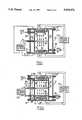
- a deposition chamber as employed for relatively small substratesconsists of an open-ended outer metal cylinder 10 provided with removable end covers 12, each of which in this embodiment also constitutes one of a pair of parallel cathode electrodes.
- the coverscan be clamped tightly in place by any suitable means which are not illustrated, and in this embodiment have electrically insulating gaskets 14 sandwiched between them and the cylinder 10 for a purpose explained below.
- the cathode end platesdo not themselves constitute the substrate for deposition, and accordingly at least one of them has a substrate element 16 mounted on its inside surface; in this embodiment both of the end plates are provided with such substrates.
- the central portions of the end plates receiving the substratesare depressed inwardly towards one another so that they are more closely spaced than the remainder of the plates.
- the resultant recesses at the outer surfacesare provided with respective electric heaters 18 supplied from a power source 20 to maintain the substrates at a temperature suitable for deposition (usually about 200°-400° C. in the case of amorphous hydrogenated silicon).
- a second open-ended replaceable cylinder 22 of any suitable materialis mounted coaxially within the outer cylinder 10 to more closely define a plasma-containing zone 24 between the two more-closely spaced portions of the two cathodes; in use the interior surface of this cylinder also becomes coated with deposited material and can be replaced when the deposit becomes too thick, reducing very considerably the deposition on the inner wall of the outer cylinder 10 and the need to clean or replace it.
- the precursor gas or gasesare introduced into the interior of the enclosure via an inlet 26 and the depleted gas or gases removed therefrom via an outlet 28.
- the procedures and apparatus for the safe supply and control of these gases, many of which are pyrophoric or highly toxic,are well documented in the art and need not be detailed in this application.
- a stabilized D.C. power supply 34is connected to the anode 30 and the two cathodes 12 to apply suitable constant potential differences between them, and produce a corresponding electric field in the zone 24, which we refer to colloquially as a "saddle” field owing to its characteristic profile between the two cathodes.
- This saddle field configurationpromotes ionization of the gas close to the anode electrode, while the oscillating trajectory of the electrons increases the effective path length for ionizing collisions, facilitating the formation of high current discharges at relatively low pressures.
- the saddle fieldalso causes positively ionized radicals to be accelerated towards the cathode electrodes, and a greater number of charged radicals are produced, so that the speed of deposition is greater and is not so dependent as the prior art D.C. process on the diffusion and drift of radicals; there is therefore much more efficient utilization of the precursor gas.
- the anode 30preferably is centrally disposed and the respective portions of the saddle field are symmetrical about the anode.
- the flow of the precursor gas from the inlet 26 to the outlet 28will substantially increase the quantity of the ions that move toward the cathode 12 downstream of the flow, as compared to the corresponding quantity of those moving upstream toward the other cathode adjacent the gas inlet, resulting in some asymmetry in the rates of deposition on the respective substrates, and an embodiment employing this flow enhancing effect to facilitate deposition or both cathodes is described below.
- the fieldneed not be symmetric, but instead can be asymmetric with the stronger portion toward the substrate supporting cathode, the asymmetry being produced either mechanically by placing the anode closer to the respective cathode, or electrically by increasing the potential difference between the two electrodes.
- the two cathodes 12are insulated from the enclosure 10 and from one another by the gaskets 14 to permit this electrically-produced asymmetry.
- the plasma containing zone 24it is undesirable for the plasma containing zone 24 to extend so far as to include the substrate since the ionized radicals then impinge on the growing film with substantial velocities and may damage it, as described above.
- Thiscan be avoided while employing relatively high fields by the embodiment of FIG. 2, in which two subsidiary ion permeable flat open grid cathode electrodes 38 are disposed close and parallel to the respective end plate cathode electrodes 12 and their respective substrates 16.
- the negative potentialsare applied to these subsidiary cathode electrodes which are both next adjacent to the anode electrode and the two first cathode electrodes 12 are grounded, and may be at zero, or at a small negative or positive potential relative to the subsidiary cathode electrodes 38.
- the plasmais now confined to the zone between the two subsidiary electrodes, which since they are permeable to both the charged and neutral radicals, permit them to pass relatively freely therethrough to the substrate with the rate of impact of the radicals on the substrate being controllable by choice of the value and size of the potential difference between the first and subsidiary electrodes. For example, a small positive potential on each end plate electrode 12 will result in a decelerating field between each subsidiary electrode 38 and its respective end plate electrode, reducing the impact of the ions on the associated substrate.
- the two subsidiary electrodesare mounted on the cylinder 22 by respective electrically insulating structures 40 so that their potentials can be adjusted individually; in the embodiment illustrated they are strapped together to be at the same potential.
- FIG. 3is an example of another apparatus characterized in that only a single substrate 16 is provided mounted on the respective first end plate cathode electrode 12.
- a movable shutter 42is provided between this first cathode electrode 12 and the associated subsidiary electrode 38 to permit the substrate to be screened for selective deposition of the material thereon.
- the flow of the precursor gasis from the anode 30 to the upper cathode 12 carrying the substrate to facilitate the flow of ions in that direction.
- the other first cathode electrode 12is not associated with a substrate and does not therefore require a subsidiary cathode 38; the electrode is of ring formation to permit the free passage or radicals therethrough.
- a removable crucible 44the contents of which are heated by an induction heater 46, is provided to permit coevaporation of the material in the crucible during the deposition.
- a single gas inlet 26is arranged to discharge the gas into the interior of the replaceable cylinder 22 adjacent the anode electrode 30, while the gas outlet 28 is disposed to communicate with the space between the cylinders 10 and 22 adjacent the gas inlet.
- the gastherefore flows substantially equally in opposite directions from the inlet towards both of the cathodes 12, thereby promoting movement of the ions generated in the neighbourhood of the anode approximately equally oppositely towards the two cathodes to provide correspondingly approximately equal rates of deposition thereon.
- one of the most commercially interesting processes involving plasma depositionis the direct formation of thin films of hydrogenated amorphous silicon, and the methods and apparatus of the invention have been used very successfully in the production of such films.
- these filmshave been produced by the dissociation of silane gas (SiH 4 ), and it has been found possible to operate effectively with gas pressures as low as 10 milliTorr, as compared to about 100 milliTorr found to be the minimum with conventional D.C. methods. Relatively high growth rates of about 5-10 Angstroms/sec. were obtained, as compared with about 2-3 Angstroms/sec. with the prior art.
- the hydrogen incorporationwas controlled by coevaporation of silicon, and films were obtained exhibiting high photoconductive gain exceeding 10 4 under Air Mass 1 illumination with a wide range of hydrogen content from about 5 to about 25 atomic percent.
- the films obtainedexhibited good adhesion and activated conduction over a wide temperature range from about 200° K. to about 450° K.
- FIG. 5is a graph showing with the production of such silicon films the current flow through the anode electrode 22 with the voltage applied between the anode and the cathodes at different silane gas pressures.
- the individual test result valuesare plotted and are not connected since they converge so much in the range 600-1000 volts as to possibly be confusing. This shows that the results obtained at the low pressure of 10 milliTorr were strictly comparable with those obtained at the higher pressures; the highest pressure usable with this apparatus was below 500 milliTorr, since at this pressure an apparent arc-type discharge was established to give excessively high current flow and the consequent high possibility of deleterious etching.
- FIG. 6is a graph, again produced in the formation of thin amorphous silicon films from silane, showing the ratio of the currents obtained at the subsidiary cathode electrodes 38 (I SH ) and at the middle anode electrode 22 (I ME ) with the voltage applied to the electrode 22 (V ME ) at various gas pressures. All three plots obtained show a peak in these ratios at a voltage that increases with increasing pressure and show that high deposition efficiencies are available at the low discharge pressures and low voltages made possible by the present invention.
- the description of the inventionhas been in general terms since it is applicable to a wide range of deposition materials, even though specific examples have been given only for the production of amorphous silicon layers employing silane.
- Examples of other processesare plasma etching, substrate cleaning and the deposition of carbon, germanium and silicon nitride.
- Plasma etchingis a chemical-type process in which surface atoms are removed by reaction with the active radicals of the plasma; it is useful for example in producing grooves in integrated circuit design.
- Substrate cleaningis a mechanical-type process employed to remove unwanted surface atoms by transferring kinetic energy of the plasma radicals to these atoms. Reference may also be made to the text book referred to above, the disclosure of which is incorporated herein by this reference.
- the drawingsshow the apparatus in a particular attitude, but the processes employed are of course not attitude-dependent and the apparatus can be employed in any other appropriate attitude and configuration.
- the electrode 30 and the permeable electrodes 38are described and illustrated herein as open grids; in the laboratory-type apparatus employed such a grid is for example of thin wires of 0.3 mm diameter spaced approximately 1-2 cm apart, and are adequate to apply the required field while being translucent, i.e. sufficiently permeable (i.e.-transparent), to the plasma electrons.
- a plain open ring electrodecan also be used provided the resultant non-uniformity of the field can be tolerated.
Landscapes
- Physics & Mathematics (AREA)
- Engineering & Computer Science (AREA)
- Plasma & Fusion (AREA)
- Chemical & Material Sciences (AREA)
- Analytical Chemistry (AREA)
- Chemical Vapour Deposition (AREA)
Abstract
Description
Claims (24)
Priority Applications (1)
| Application Number | Priority Date | Filing Date | Title |
|---|---|---|---|
| US07/565,831US5039376A (en) | 1989-09-19 | 1990-08-13 | Method and apparatus for the plasma etching, substrate cleaning, or deposition of materials by D.C. glow discharge |
Applications Claiming Priority (2)
| Application Number | Priority Date | Filing Date | Title |
|---|---|---|---|
| EP89309530AEP0418438A1 (en) | 1989-09-19 | 1989-09-19 | Method and apparatus for the plasma etching, substrate cleaning or deposition of materials by D.C. glow discharge |
| US07/565,831US5039376A (en) | 1989-09-19 | 1990-08-13 | Method and apparatus for the plasma etching, substrate cleaning, or deposition of materials by D.C. glow discharge |
Related Parent Applications (1)
| Application Number | Title | Priority Date | Filing Date |
|---|---|---|---|
| US07228414Continuation-In-Part | 1988-08-05 |
Publications (1)
| Publication Number | Publication Date |
|---|---|
| US5039376Atrue US5039376A (en) | 1991-08-13 |
Family
ID=26122357
Family Applications (1)
| Application Number | Title | Priority Date | Filing Date |
|---|---|---|---|
| US07/565,831Expired - LifetimeUS5039376A (en) | 1989-09-19 | 1990-08-13 | Method and apparatus for the plasma etching, substrate cleaning, or deposition of materials by D.C. glow discharge |
Country Status (1)
| Country | Link |
|---|---|
| US (1) | US5039376A (en) |
Cited By (26)
| Publication number | Priority date | Publication date | Assignee | Title |
|---|---|---|---|---|
| US5405447A (en)* | 1990-05-15 | 1995-04-11 | Mitsubishi Jukogyo Kabushiki Kaisha | Plasma CVD apparatus |
| US5597438A (en)* | 1995-09-14 | 1997-01-28 | Siemens Aktiengesellschaft | Etch chamber having three independently controlled electrodes |
| US5608155A (en)* | 1993-04-30 | 1997-03-04 | Applied Materials, Inc. | Method and apparatus for detecting particles on a substrate |
| WO1997008362A1 (en)* | 1995-08-28 | 1997-03-06 | Georgia Tech Research Corporation | Method and apparatus for low energy electron enhanced etching of substrates |
| US5609927A (en)* | 1995-06-06 | 1997-03-11 | Texas Instruments Incorporated | Processing methods for high-dielectric-constant materials |
| US5611426A (en)* | 1995-10-12 | 1997-03-18 | Point Group Corporation | Packaging assembly for compact discs |
| US5637237A (en)* | 1994-03-08 | 1997-06-10 | International Business Machines Corporation | Method for hot wall reactive ion etching using a dielectric or metallic liner with temperature control to achieve process stability |
| US5707692A (en)* | 1990-10-23 | 1998-01-13 | Canon Kabushiki Kaisha | Apparatus and method for processing a base substance using plasma and a magnetic field |
| US5882538A (en)* | 1995-08-28 | 1999-03-16 | Georgia Tech Research Corporation | Method and apparatus for low energy electron enhanced etching of substrates |
| US5917285A (en)* | 1996-07-24 | 1999-06-29 | Georgia Tech Research Corporation | Apparatus and method for reducing operating voltage in gas discharge devices |
| US6027663A (en)* | 1995-08-28 | 2000-02-22 | Georgia Tech Research Corporation | Method and apparatus for low energy electron enhanced etching of substrates |
| US6033587A (en)* | 1996-09-20 | 2000-03-07 | Georgia Tech Research Corporation | Method and apparatus for low energy electron enhanced etching and cleaning of substrates in the positive column of a plasma |
| US6137231A (en)* | 1996-09-10 | 2000-10-24 | The Regents Of The University Of California | Constricted glow discharge plasma source |
| US6258287B1 (en) | 1996-08-28 | 2001-07-10 | Georgia Tech Research Corporation | Method and apparatus for low energy electron enhanced etching of substrates in an AC or DC plasma environment |
| US6440864B1 (en) | 2000-06-30 | 2002-08-27 | Applied Materials Inc. | Substrate cleaning process |
| US20030121609A1 (en)* | 1999-11-26 | 2003-07-03 | Tadahiro Ohmi | Plasma etching device |
| US6692903B2 (en) | 2000-12-13 | 2004-02-17 | Applied Materials, Inc | Substrate cleaning apparatus and method |
| US20040113287A1 (en)* | 2002-11-12 | 2004-06-17 | Katsushi Kishimoto | Semiconductor device manufacturing unit and semiconductor device manufacturing method |
| US20040118678A1 (en)* | 2002-12-18 | 2004-06-24 | Klaus Hartig | Magnetron sputtering systems including anodic gas distribution systems |
| US20080029494A1 (en)* | 2006-07-21 | 2008-02-07 | Andrew William Tudhope | System and method for treating surfaces of components |
| US20080067057A1 (en)* | 2006-09-15 | 2008-03-20 | John German | Enhanced virtual anode |
| US11501959B2 (en) | 2015-02-03 | 2022-11-15 | Cardinal Cg Company | Sputtering apparatus including gas distribution system |
| US11508562B2 (en)* | 2013-08-30 | 2022-11-22 | Taiwan Semiconductor Manufacturing Company, Ltd. | Low contamination chamber for surface activation |
| US11664195B1 (en) | 2021-11-11 | 2023-05-30 | Velvetch Llc | DC plasma control for electron enhanced material processing |
| US11688588B1 (en) | 2022-02-09 | 2023-06-27 | Velvetch Llc | Electron bias control signals for electron enhanced material processing |
| US11869747B1 (en) | 2023-01-04 | 2024-01-09 | Velvetch Llc | Atomic layer etching by electron wavefront |
Citations (12)
| Publication number | Priority date | Publication date | Assignee | Title |
|---|---|---|---|---|
| JPS5220294A (en)* | 1975-08-08 | 1977-02-16 | Matsushita Electric Ind Co Ltd | Method of and apparatus for manufacturing compound thin film |
| US4070264A (en)* | 1973-07-12 | 1978-01-24 | International Business Machines Corporation | R. F. sputtering method and apparatus |
| US4223048A (en)* | 1978-08-07 | 1980-09-16 | Pacific Western Systems | Plasma enhanced chemical vapor processing of semiconductive wafers |
| US4289598A (en)* | 1980-05-03 | 1981-09-15 | Technics, Inc. | Plasma reactor and method therefor |
| JPS5914633A (en)* | 1982-07-16 | 1984-01-25 | Anelva Corp | Plasma cvd apparatus |
| US4492716A (en)* | 1979-08-16 | 1985-01-08 | Shunpei Yamazaki | Method of making non-crystalline semiconductor layer |
| US4633811A (en)* | 1984-03-28 | 1987-01-06 | Fuji Electric Co., Ltd. | Plasma CVD apparatus |
| US4633809A (en)* | 1983-05-10 | 1987-01-06 | Kabushiki Kaisha Toshiba | Amorphous silicon film forming apparatus |
| US4643952A (en)* | 1985-02-08 | 1987-02-17 | Citizen Watch Co., Ltd. | Coating film by ion plating |
| US4676195A (en)* | 1983-03-14 | 1987-06-30 | Stanley Electric Co., Ltd. | Apparatus for performing plasma chemical vapor deposition |
| US4735633A (en)* | 1987-06-23 | 1988-04-05 | Chiu Kin Chung R | Method and system for vapor extraction from gases |
| US4950376A (en)* | 1988-06-21 | 1990-08-21 | Agency Of Industrial Science & Technology | Method of gas reaction process control |
- 1990
- 1990-08-13USUS07/565,831patent/US5039376A/ennot_activeExpired - Lifetime
Patent Citations (12)
| Publication number | Priority date | Publication date | Assignee | Title |
|---|---|---|---|---|
| US4070264A (en)* | 1973-07-12 | 1978-01-24 | International Business Machines Corporation | R. F. sputtering method and apparatus |
| JPS5220294A (en)* | 1975-08-08 | 1977-02-16 | Matsushita Electric Ind Co Ltd | Method of and apparatus for manufacturing compound thin film |
| US4223048A (en)* | 1978-08-07 | 1980-09-16 | Pacific Western Systems | Plasma enhanced chemical vapor processing of semiconductive wafers |
| US4492716A (en)* | 1979-08-16 | 1985-01-08 | Shunpei Yamazaki | Method of making non-crystalline semiconductor layer |
| US4289598A (en)* | 1980-05-03 | 1981-09-15 | Technics, Inc. | Plasma reactor and method therefor |
| JPS5914633A (en)* | 1982-07-16 | 1984-01-25 | Anelva Corp | Plasma cvd apparatus |
| US4676195A (en)* | 1983-03-14 | 1987-06-30 | Stanley Electric Co., Ltd. | Apparatus for performing plasma chemical vapor deposition |
| US4633809A (en)* | 1983-05-10 | 1987-01-06 | Kabushiki Kaisha Toshiba | Amorphous silicon film forming apparatus |
| US4633811A (en)* | 1984-03-28 | 1987-01-06 | Fuji Electric Co., Ltd. | Plasma CVD apparatus |
| US4643952A (en)* | 1985-02-08 | 1987-02-17 | Citizen Watch Co., Ltd. | Coating film by ion plating |
| US4735633A (en)* | 1987-06-23 | 1988-04-05 | Chiu Kin Chung R | Method and system for vapor extraction from gases |
| US4950376A (en)* | 1988-06-21 | 1990-08-21 | Agency Of Industrial Science & Technology | Method of gas reaction process control |
Cited By (42)
| Publication number | Priority date | Publication date | Assignee | Title |
|---|---|---|---|---|
| US5405447A (en)* | 1990-05-15 | 1995-04-11 | Mitsubishi Jukogyo Kabushiki Kaisha | Plasma CVD apparatus |
| US5707692A (en)* | 1990-10-23 | 1998-01-13 | Canon Kabushiki Kaisha | Apparatus and method for processing a base substance using plasma and a magnetic field |
| US5608155A (en)* | 1993-04-30 | 1997-03-04 | Applied Materials, Inc. | Method and apparatus for detecting particles on a substrate |
| US5637237A (en)* | 1994-03-08 | 1997-06-10 | International Business Machines Corporation | Method for hot wall reactive ion etching using a dielectric or metallic liner with temperature control to achieve process stability |
| US5798016A (en)* | 1994-03-08 | 1998-08-25 | International Business Machines Corporation | Apparatus for hot wall reactive ion etching using a dielectric or metallic liner with temperature control to achieve process stability |
| US5609927A (en)* | 1995-06-06 | 1997-03-11 | Texas Instruments Incorporated | Processing methods for high-dielectric-constant materials |
| WO1997008362A1 (en)* | 1995-08-28 | 1997-03-06 | Georgia Tech Research Corporation | Method and apparatus for low energy electron enhanced etching of substrates |
| US5882538A (en)* | 1995-08-28 | 1999-03-16 | Georgia Tech Research Corporation | Method and apparatus for low energy electron enhanced etching of substrates |
| US6027663A (en)* | 1995-08-28 | 2000-02-22 | Georgia Tech Research Corporation | Method and apparatus for low energy electron enhanced etching of substrates |
| US5597438A (en)* | 1995-09-14 | 1997-01-28 | Siemens Aktiengesellschaft | Etch chamber having three independently controlled electrodes |
| US5611426A (en)* | 1995-10-12 | 1997-03-18 | Point Group Corporation | Packaging assembly for compact discs |
| US5917285A (en)* | 1996-07-24 | 1999-06-29 | Georgia Tech Research Corporation | Apparatus and method for reducing operating voltage in gas discharge devices |
| US7431796B2 (en) | 1996-08-28 | 2008-10-07 | Georgia Tech Research Corporation | Method and apparatus for low energy electron enhanced etching of substrates in an AC or DC plasma environment |
| WO2000033362A1 (en)* | 1996-08-28 | 2000-06-08 | Georgia Tech Research Corporation | Method and apparatus for low energy electron enhanced etching of substrates |
| US6258287B1 (en) | 1996-08-28 | 2001-07-10 | Georgia Tech Research Corporation | Method and apparatus for low energy electron enhanced etching of substrates in an AC or DC plasma environment |
| US6852195B2 (en) | 1996-08-28 | 2005-02-08 | Georgia Tech Research Corporation | Method and apparatus for low energy electron enhanced etching of substrates in an AC or DC plasma environment |
| US20040163763A1 (en)* | 1996-08-28 | 2004-08-26 | Martin Kevin P. | Method and apparatus for low energy electron enhanced etching of substrates in an AC or DC plasma environment |
| US6137231A (en)* | 1996-09-10 | 2000-10-24 | The Regents Of The University Of California | Constricted glow discharge plasma source |
| US6033587A (en)* | 1996-09-20 | 2000-03-07 | Georgia Tech Research Corporation | Method and apparatus for low energy electron enhanced etching and cleaning of substrates in the positive column of a plasma |
| US20030121609A1 (en)* | 1999-11-26 | 2003-07-03 | Tadahiro Ohmi | Plasma etching device |
| US8114245B2 (en)* | 1999-11-26 | 2012-02-14 | Tadahiro Ohmi | Plasma etching device |
| US6440864B1 (en) | 2000-06-30 | 2002-08-27 | Applied Materials Inc. | Substrate cleaning process |
| US6692903B2 (en) | 2000-12-13 | 2004-02-17 | Applied Materials, Inc | Substrate cleaning apparatus and method |
| US20040113287A1 (en)* | 2002-11-12 | 2004-06-17 | Katsushi Kishimoto | Semiconductor device manufacturing unit and semiconductor device manufacturing method |
| US7722738B2 (en)* | 2002-11-12 | 2010-05-25 | Sharp Kabushiki Kaisha | Semiconductor device manufacturing unit and semiconductor device manufacturing method |
| US20040118678A1 (en)* | 2002-12-18 | 2004-06-24 | Klaus Hartig | Magnetron sputtering systems including anodic gas distribution systems |
| US7166199B2 (en) | 2002-12-18 | 2007-01-23 | Cardinal Cg Company | Magnetron sputtering systems including anodic gas distribution systems |
| US20080029494A1 (en)* | 2006-07-21 | 2008-02-07 | Andrew William Tudhope | System and method for treating surfaces of components |
| US7838793B2 (en) | 2006-07-21 | 2010-11-23 | Sub-One Technology, Inc. | System and method for treating surfaces of components |
| WO2008011552A3 (en)* | 2006-07-21 | 2008-09-04 | Sub One Technology Inc | System and method for treating surfaces of components |
| US20080067057A1 (en)* | 2006-09-15 | 2008-03-20 | John German | Enhanced virtual anode |
| US7850828B2 (en) | 2006-09-15 | 2010-12-14 | Cardinal Cg Company | Enhanced virtual anode |
| US11508562B2 (en)* | 2013-08-30 | 2022-11-22 | Taiwan Semiconductor Manufacturing Company, Ltd. | Low contamination chamber for surface activation |
| US11674213B2 (en) | 2015-02-03 | 2023-06-13 | Cardinal Cg Company | Sputtering apparatus including gas distribution system |
| US11501959B2 (en) | 2015-02-03 | 2022-11-15 | Cardinal Cg Company | Sputtering apparatus including gas distribution system |
| US11664195B1 (en) | 2021-11-11 | 2023-05-30 | Velvetch Llc | DC plasma control for electron enhanced material processing |
| US11676797B2 (en) | 2021-11-11 | 2023-06-13 | Velvetch Llc | DC plasma control for electron enhanced material processing |
| US11715623B2 (en) | 2021-11-11 | 2023-08-01 | Velvetch Llc | DC plasma control for electron enhanced material processing |
| US11688588B1 (en) | 2022-02-09 | 2023-06-27 | Velvetch Llc | Electron bias control signals for electron enhanced material processing |
| US11887823B2 (en) | 2022-02-09 | 2024-01-30 | Velvetch Llc | Electron bias control signals for electron enhanced material processing |
| US11869747B1 (en) | 2023-01-04 | 2024-01-09 | Velvetch Llc | Atomic layer etching by electron wavefront |
| US11942306B1 (en) | 2023-01-04 | 2024-03-26 | Velvetch Llc | Atomic layer etching by electron wavefront |
Similar Documents
| Publication | Publication Date | Title |
|---|---|---|
| US5039376A (en) | Method and apparatus for the plasma etching, substrate cleaning, or deposition of materials by D.C. glow discharge | |
| CA1308689C (en) | Method and apparatus for forming a thin film | |
| US5102523A (en) | Arrangement for the production of a plasma | |
| JP2819420B2 (en) | Ion source | |
| EP0283519A1 (en) | Ion generation apparatus, thin film formation apparatus using the ion generation apparatus, and ion source | |
| US4979467A (en) | Thin film formation apparatus | |
| JPH05275345A (en) | Plasma cvd method and its device | |
| JPH0541705B2 (en) | ||
| US5145712A (en) | Chemical deposition of diamond | |
| JPH06275545A (en) | Formation of compound thin film using gas cluster ion | |
| JP2003527478A (en) | Apparatus for plasma-chemical deposition of polycrystalline diamond | |
| US5405447A (en) | Plasma CVD apparatus | |
| US4974544A (en) | Vapor deposition apparatus | |
| EP0959151A2 (en) | Thin film forming apparatus | |
| JPH04236781A (en) | Plasma cvd device | |
| KR900019219A (en) | Beam deposition method and apparatus for performing the same | |
| EP0418438A1 (en) | Method and apparatus for the plasma etching, substrate cleaning or deposition of materials by D.C. glow discharge | |
| EP0095384A2 (en) | Vacuum deposition apparatus | |
| US5089289A (en) | Method of forming thin films | |
| CA1341184C (en) | Method and apparatus for the plasma etching substrate cleaning or deposition of materials by d.c. glow discharge | |
| JPS61194180A (en) | Hollow electric discharge vapor deposition device | |
| JP2687129B2 (en) | Method and apparatus for producing diamond-like thin film | |
| JP3007579B2 (en) | Manufacturing method of silicon thin film | |
| JP2703029B2 (en) | Method of introducing impurities into substrate | |
| JPH0368764A (en) | Plasma treating device for forming thin film |
Legal Events
| Date | Code | Title | Description |
|---|---|---|---|
| STCF | Information on status: patent grant | Free format text:PATENTED CASE | |
| FPAY | Fee payment | Year of fee payment:4 | |
| SULP | Surcharge for late payment | ||
| REMI | Maintenance fee reminder mailed | ||
| FPAY | Fee payment | Year of fee payment:8 | |
| FPAY | Fee payment | Year of fee payment:12 | |
| AS | Assignment | Owner name:COMMERZBANK AKTIENGESELLSCHAFT, GERMANY Free format text:SECURITY AGREEMENT;ASSIGNOR:ARISE TECHNOLOGIES DEUTSCHLAND GMBH;REEL/FRAME:021064/0731 Effective date:20080602 | |
| AS | Assignment | Owner name:COMMERZBANK AKTIENGESELLSCHAFT, GERMANY Free format text:CORRECTIVE ASSIGNMENT TO CORRECT THE CONVEYING PARTY NAME FROM ARISE TECHNOLOGIES DEUTSCHLAND GMBH PREVIOUSLY RECORDED ON REEL 021064 FRAME 0731. ASSIGNOR(S) HEREBY CONFIRMS THE NAME CHANGE TO ARISE TECHNOLOGIES CORPORATION..;ASSIGNOR:ARISE TECHNOLOGIES CORPORATION;REEL/FRAME:021147/0562 Effective date:20080602 Owner name:COMMERZBANK AKTIENGESELLSCHAFT, GERMANY Free format text:CORRECTIVE ASSIGNMENT TO CORRECT THE CONVEYING PARTY NAME FROM ARISE TECHNOLOGIES DEUTSCHLAND GMBH PREVIOUSLY RECORDED ON REEL 021064 FRAME 0731;ASSIGNOR:ARISE TECHNOLOGIES CORPORATION;REEL/FRAME:021147/0562 Effective date:20080602 |