US5037169A - High speed low loss optical switch for optical communication systems - Google Patents
High speed low loss optical switch for optical communication systemsDownload PDFInfo
- Publication number
- US5037169A US5037169AUS07/482,117US48211790AUS5037169AUS 5037169 AUS5037169 AUS 5037169AUS 48211790 AUS48211790 AUS 48211790AUS 5037169 AUS5037169 AUS 5037169A
- Authority
- US
- United States
- Prior art keywords
- medium
- optical
- refraction
- index
- controllably
- Prior art date
- Legal status (The legal status is an assumption and is not a legal conclusion. Google has not performed a legal analysis and makes no representation as to the accuracy of the status listed.)
- Expired - Lifetime
Links
- 230000003287optical effectEffects0.000titleclaimsabstractdescription109
- 238000004891communicationMethods0.000titledescription5
- BJQHLKABXJIVAM-UHFFFAOYSA-Nbis(2-ethylhexyl) phthalateChemical compoundCCCCC(CC)COC(=O)C1=CC=CC=C1C(=O)OCC(CC)CCCCBJQHLKABXJIVAM-UHFFFAOYSA-N0.000claimsabstractdescription39
- 230000000737periodic effectEffects0.000claimsabstractdescription9
- 230000005684electric fieldEffects0.000claimsabstractdescription8
- 239000004065semiconductorSubstances0.000claimsabstractdescription7
- 238000000034methodMethods0.000claimsdescription13
- 239000000463materialSubstances0.000claimsdescription3
- 230000001154acute effectEffects0.000claims4
- 239000000969carrierSubstances0.000abstractdescription3
- FTWRSWRBSVXQPI-UHFFFAOYSA-Nalumanylidynearsane;gallanylidynearsaneChemical compound[As]#[Al].[As]#[Ga]FTWRSWRBSVXQPI-UHFFFAOYSA-N0.000abstractdescription2
- 230000000694effectsEffects0.000description8
- 230000008859changeEffects0.000description6
- 230000007246mechanismEffects0.000description4
- JBRZTFJDHDCESZ-UHFFFAOYSA-NAsGaChemical compound[As]#[Ga]JBRZTFJDHDCESZ-UHFFFAOYSA-N0.000description3
- 241000282461Canis lupusSpecies0.000description3
- 229910001218Gallium arsenideInorganic materials0.000description3
- 230000005540biological transmissionEffects0.000description3
- 238000010586diagramMethods0.000description3
- 238000003780insertionMethods0.000description3
- 230000037431insertionEffects0.000description3
- 239000013307optical fiberSubstances0.000description3
- 238000004458analytical methodMethods0.000description2
- 238000002310reflectometryMethods0.000description2
- 239000007787solidSubstances0.000description2
- 238000010521absorption reactionMethods0.000description1
- 230000004075alterationEffects0.000description1
- 230000008033biological extinctionEffects0.000description1
- 238000000576coating methodMethods0.000description1
- 238000010276constructionMethods0.000description1
- 230000008878couplingEffects0.000description1
- 238000010168coupling processMethods0.000description1
- 238000005859coupling reactionMethods0.000description1
- 230000001066destructive effectEffects0.000description1
- 238000002050diffraction methodMethods0.000description1
- 230000007613environmental effectEffects0.000description1
- 238000002347injectionMethods0.000description1
- 239000007924injectionSubstances0.000description1
- 238000005305interferometryMethods0.000description1
- 238000004519manufacturing processMethods0.000description1
- 239000000203mixtureSubstances0.000description1
- 238000001451molecular beam epitaxyMethods0.000description1
- 230000008569processEffects0.000description1
- 230000001902propagating effectEffects0.000description1
- 230000006798recombinationEffects0.000description1
- 238000005215recombinationMethods0.000description1
- 230000004044responseEffects0.000description1
- 238000000926separation methodMethods0.000description1
Images


Classifications
- G—PHYSICS
- G02—OPTICS
- G02F—OPTICAL DEVICES OR ARRANGEMENTS FOR THE CONTROL OF LIGHT BY MODIFICATION OF THE OPTICAL PROPERTIES OF THE MEDIA OF THE ELEMENTS INVOLVED THEREIN; NON-LINEAR OPTICS; FREQUENCY-CHANGING OF LIGHT; OPTICAL LOGIC ELEMENTS; OPTICAL ANALOGUE/DIGITAL CONVERTERS
- G02F1/00—Devices or arrangements for the control of the intensity, colour, phase, polarisation or direction of light arriving from an independent light source, e.g. switching, gating or modulating; Non-linear optics
- G02F1/29—Devices or arrangements for the control of the intensity, colour, phase, polarisation or direction of light arriving from an independent light source, e.g. switching, gating or modulating; Non-linear optics for the control of the position or the direction of light beams, i.e. deflection
- G—PHYSICS
- G02—OPTICS
- G02F—OPTICAL DEVICES OR ARRANGEMENTS FOR THE CONTROL OF LIGHT BY MODIFICATION OF THE OPTICAL PROPERTIES OF THE MEDIA OF THE ELEMENTS INVOLVED THEREIN; NON-LINEAR OPTICS; FREQUENCY-CHANGING OF LIGHT; OPTICAL LOGIC ELEMENTS; OPTICAL ANALOGUE/DIGITAL CONVERTERS
- G02F1/00—Devices or arrangements for the control of the intensity, colour, phase, polarisation or direction of light arriving from an independent light source, e.g. switching, gating or modulating; Non-linear optics
- G02F1/01—Devices or arrangements for the control of the intensity, colour, phase, polarisation or direction of light arriving from an independent light source, e.g. switching, gating or modulating; Non-linear optics for the control of the intensity, phase, polarisation or colour
- G02F1/21—Devices or arrangements for the control of the intensity, colour, phase, polarisation or direction of light arriving from an independent light source, e.g. switching, gating or modulating; Non-linear optics for the control of the intensity, phase, polarisation or colour by interference
- G—PHYSICS
- G02—OPTICS
- G02F—OPTICAL DEVICES OR ARRANGEMENTS FOR THE CONTROL OF LIGHT BY MODIFICATION OF THE OPTICAL PROPERTIES OF THE MEDIA OF THE ELEMENTS INVOLVED THEREIN; NON-LINEAR OPTICS; FREQUENCY-CHANGING OF LIGHT; OPTICAL LOGIC ELEMENTS; OPTICAL ANALOGUE/DIGITAL CONVERTERS
- G02F1/00—Devices or arrangements for the control of the intensity, colour, phase, polarisation or direction of light arriving from an independent light source, e.g. switching, gating or modulating; Non-linear optics
- G02F1/01—Devices or arrangements for the control of the intensity, colour, phase, polarisation or direction of light arriving from an independent light source, e.g. switching, gating or modulating; Non-linear optics for the control of the intensity, phase, polarisation or colour
- G02F1/0126—Opto-optical modulation, i.e. control of one light beam by another light beam, not otherwise provided for in this subclass
- G—PHYSICS
- G02—OPTICS
- G02F—OPTICAL DEVICES OR ARRANGEMENTS FOR THE CONTROL OF LIGHT BY MODIFICATION OF THE OPTICAL PROPERTIES OF THE MEDIA OF THE ELEMENTS INVOLVED THEREIN; NON-LINEAR OPTICS; FREQUENCY-CHANGING OF LIGHT; OPTICAL LOGIC ELEMENTS; OPTICAL ANALOGUE/DIGITAL CONVERTERS
- G02F1/00—Devices or arrangements for the control of the intensity, colour, phase, polarisation or direction of light arriving from an independent light source, e.g. switching, gating or modulating; Non-linear optics
- G02F1/01—Devices or arrangements for the control of the intensity, colour, phase, polarisation or direction of light arriving from an independent light source, e.g. switching, gating or modulating; Non-linear optics for the control of the intensity, phase, polarisation or colour
- G02F1/0147—Devices or arrangements for the control of the intensity, colour, phase, polarisation or direction of light arriving from an independent light source, e.g. switching, gating or modulating; Non-linear optics for the control of the intensity, phase, polarisation or colour based on thermo-optic effects
- G—PHYSICS
- G02—OPTICS
- G02F—OPTICAL DEVICES OR ARRANGEMENTS FOR THE CONTROL OF LIGHT BY MODIFICATION OF THE OPTICAL PROPERTIES OF THE MEDIA OF THE ELEMENTS INVOLVED THEREIN; NON-LINEAR OPTICS; FREQUENCY-CHANGING OF LIGHT; OPTICAL LOGIC ELEMENTS; OPTICAL ANALOGUE/DIGITAL CONVERTERS
- G02F1/00—Devices or arrangements for the control of the intensity, colour, phase, polarisation or direction of light arriving from an independent light source, e.g. switching, gating or modulating; Non-linear optics
- G02F1/01—Devices or arrangements for the control of the intensity, colour, phase, polarisation or direction of light arriving from an independent light source, e.g. switching, gating or modulating; Non-linear optics for the control of the intensity, phase, polarisation or colour
- G02F1/03—Devices or arrangements for the control of the intensity, colour, phase, polarisation or direction of light arriving from an independent light source, e.g. switching, gating or modulating; Non-linear optics for the control of the intensity, phase, polarisation or colour based on ceramics or electro-optical crystals, e.g. exhibiting Pockels effect or Kerr effect
- G—PHYSICS
- G02—OPTICS
- G02F—OPTICAL DEVICES OR ARRANGEMENTS FOR THE CONTROL OF LIGHT BY MODIFICATION OF THE OPTICAL PROPERTIES OF THE MEDIA OF THE ELEMENTS INVOLVED THEREIN; NON-LINEAR OPTICS; FREQUENCY-CHANGING OF LIGHT; OPTICAL LOGIC ELEMENTS; OPTICAL ANALOGUE/DIGITAL CONVERTERS
- G02F1/00—Devices or arrangements for the control of the intensity, colour, phase, polarisation or direction of light arriving from an independent light source, e.g. switching, gating or modulating; Non-linear optics
- G02F1/01—Devices or arrangements for the control of the intensity, colour, phase, polarisation or direction of light arriving from an independent light source, e.g. switching, gating or modulating; Non-linear optics for the control of the intensity, phase, polarisation or colour
- G02F1/21—Devices or arrangements for the control of the intensity, colour, phase, polarisation or direction of light arriving from an independent light source, e.g. switching, gating or modulating; Non-linear optics for the control of the intensity, phase, polarisation or colour by interference
- G02F1/213—Fabry-Perot type
- G—PHYSICS
- G02—OPTICS
- G02F—OPTICAL DEVICES OR ARRANGEMENTS FOR THE CONTROL OF LIGHT BY MODIFICATION OF THE OPTICAL PROPERTIES OF THE MEDIA OF THE ELEMENTS INVOLVED THEREIN; NON-LINEAR OPTICS; FREQUENCY-CHANGING OF LIGHT; OPTICAL LOGIC ELEMENTS; OPTICAL ANALOGUE/DIGITAL CONVERTERS
- G02F2202/00—Materials and properties
- G02F2202/10—Materials and properties semiconductor
- G02F2202/101—Ga×As and alloy
Definitions
- the inventionrelates to optical communication systems particularly with respect to switching optical data signals between optical channels with high speed and low insertion loss.
- the prior artalso contemplates non-mechanical switching arrangements utilizing an electro-optic effect or an acoustic-optic effect.
- Such prior art optical switcheswhich utilize diffraction tend to lose optical intensity into the side lobes thereof resulting in less signal into the intended output channel.
- Such switches utilizing diffraction methodsalso tend to deflect a portion of the optical signal into non-selected output channels resulting in non-zero extinction ratios for these channels.
- the prior art optical switches utilizing the electro-optic effectthe light signal is coupled into and out of a lossy electro-optic medium thereby introducing undesirably high insertion losses.
- Another disadvantage of the prior art optical switchesis that, generally, a stable electronic signal must be maintained for the switched and unswitched states of the devices.
- a controlled voltagemust be applied to change output channels.
- electro-optic switchesrequire precision voltage control circuitry.
- a controlled electronic frequency signalis required for diffraction of the light in the desired direction.
- acousto-optic switchesrequire a precise electronic frequency signal generator.
- a high speed and low insertion loss optical switchis provided by utilizing a Fabry-Perot
- the switchincludes means for controlling the index of refraction of the medium so as to switch the input light beam between the reflected beam and the transmitted beam thereby switching the input light beam between two output channels.
- the etalon cavity mediumpreferably comprises a semiconductor material with controllable index of refraction and the control means preferably comprises an optical pump injecting an optical pump control beam into the medium.
- switching controlmay be effected by an electric field (electro-optic effect) or thermal field applied to the medium or by the injection of electrons and holes into the medium.
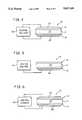
- FIG. 1is a schematic illustration of a Fabry-Perot etalon implemented in accordance with the present invention, where switching control is effected by an optical pump beam.
- FIG. 2is a graph of the ratio of the reflected intensity to the incident intensity versus index of refraction of the etalon medium illustrating operation in accordance with the invention.
- FIG. 3is a schematic illustration of a periodic multilayer forming the etalon reflective surfaces.
- FIG. 4is a schematic diagram of the etalon of FIG. 1 with an alternative switching control mechanism.
- FIG. 5is a schematic diagram of the etalon of FIG. 1 with a further alternative switching control mechanism.
- FIG. 6is a schematic diagram of the etalon of FIG. 1 with another alternative switching control mechanism.
- a Fabry-Perot interferometer or etalon 10is illustrated, implemented in accordance with the invention to switch an input data optical beam on an input optical conduit 11 between output optical conduits 12 and 13.
- the conduits 11-13may, for example, comprise optical fibers.
- the etalon 10is comprised of plane parallel reflecting surfaces 14 and 15 with a separation h therebetween forming an optical cavity 16.
- the optical cavity 16includes an optical medium 17 having an index of refraction of n'.
- the etalon 10is in a surrounding medium with an index of refraction of n.
- Monochromatic incident light from the input conduit 11impinges on the reflective surface 14 at an angle ⁇ .
- the incident monochromatic lightis transmitted and reflected by the plane parallel reflectors 14 and 15 undergoing constructive and destructive interference resulting in the light intensity being distributed between focal points P and p' of lenses 18 and 19, respectively.
- the incident light transmitted through the etalon 10 to the point Pcomprises a transmitted optical beam 20.
- the incident light reflected from the etalon 10 to the point p'forms a reflected optical beam 21. It is appreciated that the Fabry-Perot etalon transmits and reflects light signals with very low loss.
- the index of refraction n' of the medium 17 between the reflective surfaces 14 and 15 of the etalon 10is varied in a controlled manner so that the incident light from the input conduit 11 is substantially completely switched between the points P and p'.
- the incident beam from the input conduit 11is reflected from the reflective surface 14 and focused by the lens 19 to form the reflected beam 21.
- the reflected beam 21provides the output optical signal on the output optical conduit 12.
- the transmitted beam 20 focused by the lens 18provides the output optical signal on the output optical conduit 13.
- the input optical beam from the input conduit 11is switched between output conduits 12 and 13 in accordance with whether the etalon 10 is in the reflective or transmissive mode, respectively.
- the etalon 10is switched between reflection and transmission preferably by an optical pump 22 that injects a control optical pump beam 23 into the medium 17.
- the optical pump beam 23varies the index of refraction of the medium 17 to effect the switching.
- a preferred embodiment of the inventionis fabricated with an etalon comprised of epitaxially deposited layers of Aluminum Gallium Arsenide (Al x Ga 1-x As) with the incident optical input signal from the input conduit 11 having a wavelength of 850 nm.
- the spacing between the reflective surfaces 14 and 15is 4.0 um and the index of refraction n is equal to 1.
- the reflecting surfaces 14 and 15are non-absorbing and have a reflectance of 0.8. A method of constructing such a reflecting surface on Al x Ga 1-x As will be later described. For construction convenience it is desirable that the angle of deflection 2 ⁇ be approximately 90°. For this angle of deflection, ⁇ is chosen as 43°.
- the ratio of optical intensity I.sup.(r) deflected to P' to incident optical intensity I.sup.(i) as a function of n'is calculated and the result illustrated in FIG. 2.
- n'is increased by more than 0.03, the intensity into p' abruptly increases to almost the total incident intensity while the beam into P diminishes to almost zero.
- the increase in n'is effected by the optical pump 22.
- the etalon 10is quiescently transmissive thereby coupling the input conduit 11 to the output conduit 13 in the quiescent state of the etalon.
- Quiescent thermal equilibriumis readily maintained since in practical usage the device will probably reside in a thermally controlled environment such as the switch equipment room of a modern communication network. If a thermally controlled environment cannot be maintained, then feedback techniques can be used to compensate for temperature fluctuations in the environment.
- An example of such a techniqueis as follows. With reference to FIG. 2, it is appreciated that the intensity of the reflected optical power is a periodic function of n'. Suppose the medium is at an initial temperature T.
- n'would change to, say, 3.60.
- the optical intensity of the transmitted beam 20can be monitored, the loss of intensity can be detected, and a signal can be conveyed from the monitor to the optical pump 22.
- the signalwill instruct the optical pump 22 to increase the intensity of the optical pump beam 23 so as to increase the intensity of the transmitted beam 20.
- the reflective modecan similarly be maintained against temperature fluctuations by using such feedback techniques. In this mode the intensity of the reflected beam 21 can be monitored in order to maintain the intensity of the reflected beam 21 at a maximum.
- the reflective surfaces 14 and 15have a low absorption and a high reflectance of approximately 0.8 or greater.
- Each of such surfaces of the etalon 10can be fabricated as a periodic multilayer of non-absorbing films as illustrated in FIG. 3. Such multilayers are described in the above referenced Born and Wolf text in Section 1.6.5 thereof on pages 66-70.
- the layers h 2 and h 3are a quarter of a wavelength of the monochromatic incident light.
- the layersare arranged in succession characterized by the sequence n 3 , n 2 , n 3 , . . . , n 2 , n 3 , n 2 of refractive indices.
- the embodiment of FIG. 1was described in terms of utilizing the optical pump 22 to induce a change in the index of refraction of the medium 17 so as to switch the outputs of the Fabry-Perot etalon 10 between the output conduits 12 and 13.
- the change in index of refractioncan alternatively be effected by (i) applying an electric field in the medium 17 (the electro-optic effect), (ii) increasing the temperature of the medium 17 to thermally excite free carriers, or (iii) increasing the free carrier concentration in the medium 17 by, for example, injecting electrons and holes from an external electrical circuit.
- FIG. 4in which like reference numerals indicate like elements with respect to FIG. 1, an alternative embodiment of the invention is illustrated where variation in the index of refraction of the medium 17 is effected by applying an electric field in the medium 17 (the electro-optic effect).
- a circuit 30applies a control voltage across electrodes 31 and 32 to vary the electric field in the medium 17 thereby controlling the switching of the etalon 10.
- FIG. 5in which like reference numerals indicate like elements with respect to FIG. 1, an alternative embodiment of the invention is illustrated where the variation in the index of refraction is effected by varying the temperature of the medium 17.
- a heater 40 controlled by a heater control circuit 41is included to provide the temperature variation.
- FIG. 6in which like reference numerals indicate like elements with respect to FIG. 1, an alternative embodiment of the invention is illustrated where variation in the index of refraction of the medium 17 is effected by injecting carriers, electrons and holes, from an external electrical control circuit 50.
- the circuit 50passes a control current through the medium 17 by means of electrodes 51 and 52 thereby controlling the switching of the etalon 10.
- the present inventionprovides optical frequency selectivity of the transmission and reflection of the output beams.
- the principle of lightwave interferenceis involved in switching the optical signals.
- Optical signals with wavelengths different from the wavelength to which the interferometer is tunedwill not be deflected.
- switchingis performed by the alteration of the index of refraction in the semiconductor medium 17 induced by optical, electronic or thermal means.
- the use of the dielectric multilayer structures 14 and 15provide low loss and high reflectance.
- the inventionprovides an optical switching device utilizing the non-absorbing optical resonant cavity 16, which by its operation, provides switching between transmission and reflection with very low loss.
- the switching device described hereinis highly reproducible and readily fabricated since the switch can be constructed utilizing a well developed finely controlled process such as molecular beam epitaxy. Fabrication can be performed utilizing atomic layer control of semiconductor layer thickness and composition in epitaxial growth systems.
- the inventioncan be fabricated having an extremely small size.
- the devicehas a thickness of several micrometers and lateral dimensions determined by the lateral dimensions of the two optical beams; viz, the controlling beam and the controlled beam. Such lateral dimensions are on the order of 10 to 100 micrometers.
- the switch of the present inventionhas a very high speed of response. The switching speed is limited by the electron-hole recombination time which is on the order of one nanosecond in Gallium Arsenide.
- the present inventionprovides the capability in optical communication and optical computing systems for switching optical signals from one channel to several other channels with low loss. Accordingly, the optical switch illustrated herein is cascadable to switch an optical signal from one channel to one of several channels. Additionally, it is appreciated that the optical switch of the present invention is bi-directional in that it performs the same operation on forward and reverse propagating signals.
- the inventionprovides a solid state device that is stable against temperature, pressure, and electromagnetic disturbances. The resonant condition in the etalon is maintained by the thickness of a semiconductor solid which cannot be altered without extreme environmental conditions.
- control signalis zero for one state of the device or above a threshold for the other state.
- the ultimate magnitude of the control signalis not critical.
- the embodiment of FIG. 1is an all optical device utilizing an optical controlling beam.
- the inventionis compatible with signal processors with optical outputs.
- the present inventionprovides an optical switch with high switching speed, small size, low cost, high reliability, and the ability to be controlled by another optical signal--light controlling light.
Landscapes
- Physics & Mathematics (AREA)
- Nonlinear Science (AREA)
- General Physics & Mathematics (AREA)
- Optics & Photonics (AREA)
- Mechanical Light Control Or Optical Switches (AREA)
Abstract
Description
Claims (17)
Priority Applications (1)
| Application Number | Priority Date | Filing Date | Title |
|---|---|---|---|
| US07/482,117US5037169A (en) | 1990-02-20 | 1990-02-20 | High speed low loss optical switch for optical communication systems |
Applications Claiming Priority (1)
| Application Number | Priority Date | Filing Date | Title |
|---|---|---|---|
| US07/482,117US5037169A (en) | 1990-02-20 | 1990-02-20 | High speed low loss optical switch for optical communication systems |
Publications (1)
| Publication Number | Publication Date |
|---|---|
| US5037169Atrue US5037169A (en) | 1991-08-06 |
Family
ID=23914744
Family Applications (1)
| Application Number | Title | Priority Date | Filing Date |
|---|---|---|---|
| US07/482,117Expired - LifetimeUS5037169A (en) | 1990-02-20 | 1990-02-20 | High speed low loss optical switch for optical communication systems |
Country Status (1)
| Country | Link |
|---|---|
| US (1) | US5037169A (en) |
Cited By (67)
| Publication number | Priority date | Publication date | Assignee | Title |
|---|---|---|---|---|
| US5321774A (en)* | 1993-07-30 | 1994-06-14 | National Research Council Of Canada | Polarization independent transmissive/reflective optical switch |
| US5909303A (en)* | 1996-01-04 | 1999-06-01 | The Board Of Trustees Of The Leland Stanford Junior University | Optical modulator and optical modulator array |
| US5959756A (en)* | 1997-12-01 | 1999-09-28 | Keyworth; Barrie | Optical deflection switch |
| US6081634A (en)* | 1998-09-25 | 2000-06-27 | The United States Of America As Represented By The National Security Agency | All-fiber optically-controlled optical switch |
| US6211993B1 (en) | 1996-05-20 | 2001-04-03 | Nz Applied Technologies Corporation | Thin film ferroelectric light modulators |
| WO2001075513A1 (en)* | 2000-04-03 | 2001-10-11 | Massachusetts Institute Of Technology | All optical switch for optical integrated circuits |
| EP1159582A4 (en)* | 1999-01-13 | 2002-04-03 | Hays Fisk Moore Llc | Coupled etalon interferometers |
| DE10102723A1 (en)* | 2001-01-22 | 2002-08-22 | Zeiss Carl | Beam deflector, switching arrangement with beam deflector and method for optionally linking connections for optical signals |
| US6486984B1 (en) | 1999-06-07 | 2002-11-26 | Agilent Technologies, Inc. | Wavelength monitor using hybrid approach |
| WO2002103441A1 (en)* | 2001-06-18 | 2002-12-27 | Aegis Semiconductor, Inc. | Index tunable thin film interference coatings |
| US6643054B1 (en) | 2001-01-22 | 2003-11-04 | Carl-Zeiss-Stiftung | Beam deflector, switching system comprising beam deflectors as well as method for selectively coupling terminals for optical signals |
| US20040062945A1 (en)* | 2001-06-18 | 2004-04-01 | Aegis Semiconductor | Index tunable thin film interference coatings |
| US20040165245A1 (en)* | 1999-11-03 | 2004-08-26 | Carlson Steven Allen | Electro-optic reflective modulators |
| US20050030628A1 (en)* | 2003-06-20 | 2005-02-10 | Aegis Semiconductor | Very low cost narrow band infrared sensor |
| US20050074206A1 (en)* | 2003-09-08 | 2005-04-07 | Aegis Semiconductor, Inc. | Tunable dispersion compensator |
| US20050082480A1 (en)* | 2003-08-26 | 2005-04-21 | Aegis Semiconductor, Inc. | Infrared camera system |
| US20050105185A1 (en)* | 2003-10-07 | 2005-05-19 | Aegis Semiconductor, Inc | Tunable optical filter with heater on a CTE-matched transparent substrate |
| WO2014107287A1 (en) | 2012-12-20 | 2014-07-10 | Kemp Nathaniel J | Optical coherence tomography system that is reconfigurable between different imaging modes |
| US9286673B2 (en) | 2012-10-05 | 2016-03-15 | Volcano Corporation | Systems for correcting distortions in a medical image and methods of use thereof |
| US9292918B2 (en) | 2012-10-05 | 2016-03-22 | Volcano Corporation | Methods and systems for transforming luminal images |
| US9301687B2 (en) | 2013-03-13 | 2016-04-05 | Volcano Corporation | System and method for OCT depth calibration |
| US9307926B2 (en) | 2012-10-05 | 2016-04-12 | Volcano Corporation | Automatic stent detection |
| US9324141B2 (en) | 2012-10-05 | 2016-04-26 | Volcano Corporation | Removal of A-scan streaking artifact |
| US9360630B2 (en) | 2011-08-31 | 2016-06-07 | Volcano Corporation | Optical-electrical rotary joint and methods of use |
| US9367965B2 (en) | 2012-10-05 | 2016-06-14 | Volcano Corporation | Systems and methods for generating images of tissue |
| US9383263B2 (en) | 2012-12-21 | 2016-07-05 | Volcano Corporation | Systems and methods for narrowing a wavelength emission of light |
| JP2016161802A (en)* | 2015-03-03 | 2016-09-05 | 富士通株式会社 | Variable optical attenuator and optical module |
| US9478940B2 (en) | 2012-10-05 | 2016-10-25 | Volcano Corporation | Systems and methods for amplifying light |
| US9486143B2 (en) | 2012-12-21 | 2016-11-08 | Volcano Corporation | Intravascular forward imaging device |
| CN106444207A (en)* | 2016-10-18 | 2017-02-22 | 中国科学院半导体研究所 | Integrated all-optical switch |
| US9596993B2 (en) | 2007-07-12 | 2017-03-21 | Volcano Corporation | Automatic calibration systems and methods of use |
| US9612105B2 (en) | 2012-12-21 | 2017-04-04 | Volcano Corporation | Polarization sensitive optical coherence tomography system |
| US9622706B2 (en) | 2007-07-12 | 2017-04-18 | Volcano Corporation | Catheter for in vivo imaging |
| US9730613B2 (en) | 2012-12-20 | 2017-08-15 | Volcano Corporation | Locating intravascular images |
| US9770172B2 (en) | 2013-03-07 | 2017-09-26 | Volcano Corporation | Multimodal segmentation in intravascular images |
| US9858668B2 (en) | 2012-10-05 | 2018-01-02 | Volcano Corporation | Guidewire artifact removal in images |
| US9867530B2 (en) | 2006-08-14 | 2018-01-16 | Volcano Corporation | Telescopic side port catheter device with imaging system and method for accessing side branch occlusions |
| US10058284B2 (en) | 2012-12-21 | 2018-08-28 | Volcano Corporation | Simultaneous imaging, monitoring, and therapy |
| US10070827B2 (en) | 2012-10-05 | 2018-09-11 | Volcano Corporation | Automatic image playback |
| US10166003B2 (en) | 2012-12-21 | 2019-01-01 | Volcano Corporation | Ultrasound imaging with variable line density |
| US10191220B2 (en) | 2012-12-21 | 2019-01-29 | Volcano Corporation | Power-efficient optical circuit |
| US10219887B2 (en) | 2013-03-14 | 2019-03-05 | Volcano Corporation | Filters with echogenic characteristics |
| US10219780B2 (en) | 2007-07-12 | 2019-03-05 | Volcano Corporation | OCT-IVUS catheter for concurrent luminal imaging |
| US10226597B2 (en) | 2013-03-07 | 2019-03-12 | Volcano Corporation | Guidewire with centering mechanism |
| US10243660B2 (en) | 2016-02-03 | 2019-03-26 | Northwester University | Ultrafast all-optical modulation of the visible and infrared spectrum with nanorod arrays |
| US10238367B2 (en) | 2012-12-13 | 2019-03-26 | Volcano Corporation | Devices, systems, and methods for targeted cannulation |
| US10292677B2 (en) | 2013-03-14 | 2019-05-21 | Volcano Corporation | Endoluminal filter having enhanced echogenic properties |
| US10332228B2 (en) | 2012-12-21 | 2019-06-25 | Volcano Corporation | System and method for graphical processing of medical data |
| US10413317B2 (en) | 2012-12-21 | 2019-09-17 | Volcano Corporation | System and method for catheter steering and operation |
| US10420530B2 (en) | 2012-12-21 | 2019-09-24 | Volcano Corporation | System and method for multipath processing of image signals |
| US10426590B2 (en) | 2013-03-14 | 2019-10-01 | Volcano Corporation | Filters with echogenic characteristics |
| US10568586B2 (en) | 2012-10-05 | 2020-02-25 | Volcano Corporation | Systems for indicating parameters in an imaging data set and methods of use |
| US10595820B2 (en) | 2012-12-20 | 2020-03-24 | Philips Image Guided Therapy Corporation | Smooth transition catheters |
| US10638939B2 (en) | 2013-03-12 | 2020-05-05 | Philips Image Guided Therapy Corporation | Systems and methods for diagnosing coronary microvascular disease |
| US10724082B2 (en) | 2012-10-22 | 2020-07-28 | Bio-Rad Laboratories, Inc. | Methods for analyzing DNA |
| US10758207B2 (en) | 2013-03-13 | 2020-09-01 | Philips Image Guided Therapy Corporation | Systems and methods for producing an image from a rotational intravascular ultrasound device |
| US10942022B2 (en) | 2012-12-20 | 2021-03-09 | Philips Image Guided Therapy Corporation | Manual calibration of imaging system |
| US10939826B2 (en) | 2012-12-20 | 2021-03-09 | Philips Image Guided Therapy Corporation | Aspirating and removing biological material |
| US10993694B2 (en) | 2012-12-21 | 2021-05-04 | Philips Image Guided Therapy Corporation | Rotational ultrasound imaging catheter with extended catheter body telescope |
| US11026591B2 (en) | 2013-03-13 | 2021-06-08 | Philips Image Guided Therapy Corporation | Intravascular pressure sensor calibration |
| US11040140B2 (en) | 2010-12-31 | 2021-06-22 | Philips Image Guided Therapy Corporation | Deep vein thrombosis therapeutic methods |
| US11141063B2 (en) | 2010-12-23 | 2021-10-12 | Philips Image Guided Therapy Corporation | Integrated system architectures and methods of use |
| US11154313B2 (en) | 2013-03-12 | 2021-10-26 | The Volcano Corporation | Vibrating guidewire torquer and methods of use |
| US11272845B2 (en) | 2012-10-05 | 2022-03-15 | Philips Image Guided Therapy Corporation | System and method for instant and automatic border detection |
| US11406498B2 (en) | 2012-12-20 | 2022-08-09 | Philips Image Guided Therapy Corporation | Implant delivery system and implants |
| US12201477B2 (en) | 2012-10-05 | 2025-01-21 | Philips Image Guided Therapy Corporation | Methods and systems for establishing parameters for three-dimensional imaging |
| US12343198B2 (en) | 2013-03-14 | 2025-07-01 | Philips Image Guided Therapy Corporation | Delivery catheter having imaging capabilities |
Citations (4)
| Publication number | Priority date | Publication date | Assignee | Title |
|---|---|---|---|---|
| US4525687A (en)* | 1983-02-28 | 1985-06-25 | At&T Bell Laboratories | High speed light modulator using multiple quantum well structures |
| US4573767A (en)* | 1984-05-31 | 1986-03-04 | The United States Of America As Represented By The Secretary Of The Air Force | Optical flip-flop system |
| US4585301A (en)* | 1985-04-23 | 1986-04-29 | Utah State Universtiy Foundation | Optically actuated optical switch apparatus and methods |
| US4947223A (en)* | 1987-08-31 | 1990-08-07 | The United States Of America As Represented By The United States Department Of Energy | Semiconductor devices incorporating multilayer interference regions |
- 1990
- 1990-02-20USUS07/482,117patent/US5037169A/ennot_activeExpired - Lifetime
Patent Citations (4)
| Publication number | Priority date | Publication date | Assignee | Title |
|---|---|---|---|---|
| US4525687A (en)* | 1983-02-28 | 1985-06-25 | At&T Bell Laboratories | High speed light modulator using multiple quantum well structures |
| US4573767A (en)* | 1984-05-31 | 1986-03-04 | The United States Of America As Represented By The Secretary Of The Air Force | Optical flip-flop system |
| US4585301A (en)* | 1985-04-23 | 1986-04-29 | Utah State Universtiy Foundation | Optically actuated optical switch apparatus and methods |
| US4947223A (en)* | 1987-08-31 | 1990-08-07 | The United States Of America As Represented By The United States Department Of Energy | Semiconductor devices incorporating multilayer interference regions |
Cited By (87)
| Publication number | Priority date | Publication date | Assignee | Title |
|---|---|---|---|---|
| US5321774A (en)* | 1993-07-30 | 1994-06-14 | National Research Council Of Canada | Polarization independent transmissive/reflective optical switch |
| US5909303A (en)* | 1996-01-04 | 1999-06-01 | The Board Of Trustees Of The Leland Stanford Junior University | Optical modulator and optical modulator array |
| US6535321B2 (en) | 1996-05-20 | 2003-03-18 | Corning Applied Technologies Corporation | Thin film ferroelectric light modulators |
| US6211993B1 (en) | 1996-05-20 | 2001-04-03 | Nz Applied Technologies Corporation | Thin film ferroelectric light modulators |
| US6411422B2 (en) | 1996-05-20 | 2002-06-25 | Corning Applied Technologies Corporation | Thin film ferroelectric light modulators |
| US5959756A (en)* | 1997-12-01 | 1999-09-28 | Keyworth; Barrie | Optical deflection switch |
| US6081634A (en)* | 1998-09-25 | 2000-06-27 | The United States Of America As Represented By The National Security Agency | All-fiber optically-controlled optical switch |
| EP1159582A4 (en)* | 1999-01-13 | 2002-04-03 | Hays Fisk Moore Llc | Coupled etalon interferometers |
| US6486984B1 (en) | 1999-06-07 | 2002-11-26 | Agilent Technologies, Inc. | Wavelength monitor using hybrid approach |
| US6950228B2 (en)* | 1999-11-03 | 2005-09-27 | Optodot Corporation | Electro-optic reflective modulators |
| US20040165245A1 (en)* | 1999-11-03 | 2004-08-26 | Carlson Steven Allen | Electro-optic reflective modulators |
| WO2001075513A1 (en)* | 2000-04-03 | 2001-10-11 | Massachusetts Institute Of Technology | All optical switch for optical integrated circuits |
| US6684003B2 (en) | 2000-04-03 | 2004-01-27 | Massachusetts Institute Of Technology | All optical switch for optical integrated circuits |
| US6643054B1 (en) | 2001-01-22 | 2003-11-04 | Carl-Zeiss-Stiftung | Beam deflector, switching system comprising beam deflectors as well as method for selectively coupling terminals for optical signals |
| EP1225474A3 (en)* | 2001-01-22 | 2004-09-01 | Carl Zeiss | Optical beam deflector |
| DE10102723A1 (en)* | 2001-01-22 | 2002-08-22 | Zeiss Carl | Beam deflector, switching arrangement with beam deflector and method for optionally linking connections for optical signals |
| US20040062945A1 (en)* | 2001-06-18 | 2004-04-01 | Aegis Semiconductor | Index tunable thin film interference coatings |
| WO2002103441A1 (en)* | 2001-06-18 | 2002-12-27 | Aegis Semiconductor, Inc. | Index tunable thin film interference coatings |
| US7049004B2 (en) | 2001-06-18 | 2006-05-23 | Aegis Semiconductor, Inc. | Index tunable thin film interference coatings |
| US20050030628A1 (en)* | 2003-06-20 | 2005-02-10 | Aegis Semiconductor | Very low cost narrow band infrared sensor |
| US20050082480A1 (en)* | 2003-08-26 | 2005-04-21 | Aegis Semiconductor, Inc. | Infrared camera system |
| US20070023661A1 (en)* | 2003-08-26 | 2007-02-01 | Redshift Systems Corporation | Infrared camera system |
| US7221827B2 (en) | 2003-09-08 | 2007-05-22 | Aegis Semiconductor, Inc. | Tunable dispersion compensator |
| US20050074206A1 (en)* | 2003-09-08 | 2005-04-07 | Aegis Semiconductor, Inc. | Tunable dispersion compensator |
| US7304799B2 (en) | 2003-10-07 | 2007-12-04 | Aegis Lightwave, Inc. | Tunable optical filter with heater on a CTE-matched transparent substrate |
| US20050105185A1 (en)* | 2003-10-07 | 2005-05-19 | Aegis Semiconductor, Inc | Tunable optical filter with heater on a CTE-matched transparent substrate |
| US9867530B2 (en) | 2006-08-14 | 2018-01-16 | Volcano Corporation | Telescopic side port catheter device with imaging system and method for accessing side branch occlusions |
| US11350906B2 (en) | 2007-07-12 | 2022-06-07 | Philips Image Guided Therapy Corporation | OCT-IVUS catheter for concurrent luminal imaging |
| US10219780B2 (en) | 2007-07-12 | 2019-03-05 | Volcano Corporation | OCT-IVUS catheter for concurrent luminal imaging |
| US9622706B2 (en) | 2007-07-12 | 2017-04-18 | Volcano Corporation | Catheter for in vivo imaging |
| US9596993B2 (en) | 2007-07-12 | 2017-03-21 | Volcano Corporation | Automatic calibration systems and methods of use |
| US11141063B2 (en) | 2010-12-23 | 2021-10-12 | Philips Image Guided Therapy Corporation | Integrated system architectures and methods of use |
| US11040140B2 (en) | 2010-12-31 | 2021-06-22 | Philips Image Guided Therapy Corporation | Deep vein thrombosis therapeutic methods |
| US9360630B2 (en) | 2011-08-31 | 2016-06-07 | Volcano Corporation | Optical-electrical rotary joint and methods of use |
| US9307926B2 (en) | 2012-10-05 | 2016-04-12 | Volcano Corporation | Automatic stent detection |
| US9292918B2 (en) | 2012-10-05 | 2016-03-22 | Volcano Corporation | Methods and systems for transforming luminal images |
| US9478940B2 (en) | 2012-10-05 | 2016-10-25 | Volcano Corporation | Systems and methods for amplifying light |
| US11510632B2 (en) | 2012-10-05 | 2022-11-29 | Philips Image Guided Therapy Corporation | Systems for indicating parameters in an imaging data set and methods of use |
| US11890117B2 (en) | 2012-10-05 | 2024-02-06 | Philips Image Guided Therapy Corporation | Systems for indicating parameters in an imaging data set and methods of use |
| US9367965B2 (en) | 2012-10-05 | 2016-06-14 | Volcano Corporation | Systems and methods for generating images of tissue |
| US11272845B2 (en) | 2012-10-05 | 2022-03-15 | Philips Image Guided Therapy Corporation | System and method for instant and automatic border detection |
| US9324141B2 (en) | 2012-10-05 | 2016-04-26 | Volcano Corporation | Removal of A-scan streaking artifact |
| US12201477B2 (en) | 2012-10-05 | 2025-01-21 | Philips Image Guided Therapy Corporation | Methods and systems for establishing parameters for three-dimensional imaging |
| US11864870B2 (en) | 2012-10-05 | 2024-01-09 | Philips Image Guided Therapy Corporation | System and method for instant and automatic border detection |
| US9286673B2 (en) | 2012-10-05 | 2016-03-15 | Volcano Corporation | Systems for correcting distortions in a medical image and methods of use thereof |
| US9858668B2 (en) | 2012-10-05 | 2018-01-02 | Volcano Corporation | Guidewire artifact removal in images |
| US12226189B2 (en) | 2012-10-05 | 2025-02-18 | Philips Image Guided Therapy Corporation | System and method for instant and automatic border detection |
| US10568586B2 (en) | 2012-10-05 | 2020-02-25 | Volcano Corporation | Systems for indicating parameters in an imaging data set and methods of use |
| US10070827B2 (en) | 2012-10-05 | 2018-09-11 | Volcano Corporation | Automatic image playback |
| US10724082B2 (en) | 2012-10-22 | 2020-07-28 | Bio-Rad Laboratories, Inc. | Methods for analyzing DNA |
| US10238367B2 (en) | 2012-12-13 | 2019-03-26 | Volcano Corporation | Devices, systems, and methods for targeted cannulation |
| US9709379B2 (en) | 2012-12-20 | 2017-07-18 | Volcano Corporation | Optical coherence tomography system that is reconfigurable between different imaging modes |
| US10595820B2 (en) | 2012-12-20 | 2020-03-24 | Philips Image Guided Therapy Corporation | Smooth transition catheters |
| US11406498B2 (en) | 2012-12-20 | 2022-08-09 | Philips Image Guided Therapy Corporation | Implant delivery system and implants |
| US11141131B2 (en) | 2012-12-20 | 2021-10-12 | Philips Image Guided Therapy Corporation | Smooth transition catheters |
| US9730613B2 (en) | 2012-12-20 | 2017-08-15 | Volcano Corporation | Locating intravascular images |
| WO2014107287A1 (en) | 2012-12-20 | 2014-07-10 | Kemp Nathaniel J | Optical coherence tomography system that is reconfigurable between different imaging modes |
| US10939826B2 (en) | 2012-12-20 | 2021-03-09 | Philips Image Guided Therapy Corporation | Aspirating and removing biological material |
| US10942022B2 (en) | 2012-12-20 | 2021-03-09 | Philips Image Guided Therapy Corporation | Manual calibration of imaging system |
| US11892289B2 (en) | 2012-12-20 | 2024-02-06 | Philips Image Guided Therapy Corporation | Manual calibration of imaging system |
| US10420530B2 (en) | 2012-12-21 | 2019-09-24 | Volcano Corporation | System and method for multipath processing of image signals |
| US9486143B2 (en) | 2012-12-21 | 2016-11-08 | Volcano Corporation | Intravascular forward imaging device |
| US11786213B2 (en) | 2012-12-21 | 2023-10-17 | Philips Image Guided Therapy Corporation | System and method for multipath processing of image signals |
| US9383263B2 (en) | 2012-12-21 | 2016-07-05 | Volcano Corporation | Systems and methods for narrowing a wavelength emission of light |
| US10058284B2 (en) | 2012-12-21 | 2018-08-28 | Volcano Corporation | Simultaneous imaging, monitoring, and therapy |
| US10166003B2 (en) | 2012-12-21 | 2019-01-01 | Volcano Corporation | Ultrasound imaging with variable line density |
| US10413317B2 (en) | 2012-12-21 | 2019-09-17 | Volcano Corporation | System and method for catheter steering and operation |
| US10332228B2 (en) | 2012-12-21 | 2019-06-25 | Volcano Corporation | System and method for graphical processing of medical data |
| US10993694B2 (en) | 2012-12-21 | 2021-05-04 | Philips Image Guided Therapy Corporation | Rotational ultrasound imaging catheter with extended catheter body telescope |
| US9612105B2 (en) | 2012-12-21 | 2017-04-04 | Volcano Corporation | Polarization sensitive optical coherence tomography system |
| US11253225B2 (en) | 2012-12-21 | 2022-02-22 | Philips Image Guided Therapy Corporation | System and method for multipath processing of image signals |
| US10191220B2 (en) | 2012-12-21 | 2019-01-29 | Volcano Corporation | Power-efficient optical circuit |
| US9770172B2 (en) | 2013-03-07 | 2017-09-26 | Volcano Corporation | Multimodal segmentation in intravascular images |
| US10226597B2 (en) | 2013-03-07 | 2019-03-12 | Volcano Corporation | Guidewire with centering mechanism |
| US12350018B2 (en) | 2013-03-12 | 2025-07-08 | Philips Image Guided Therapy Corporation | Systems and methods for diagnosing coronary microvascular disease |
| US11154313B2 (en) | 2013-03-12 | 2021-10-26 | The Volcano Corporation | Vibrating guidewire torquer and methods of use |
| US10638939B2 (en) | 2013-03-12 | 2020-05-05 | Philips Image Guided Therapy Corporation | Systems and methods for diagnosing coronary microvascular disease |
| US10758207B2 (en) | 2013-03-13 | 2020-09-01 | Philips Image Guided Therapy Corporation | Systems and methods for producing an image from a rotational intravascular ultrasound device |
| US11026591B2 (en) | 2013-03-13 | 2021-06-08 | Philips Image Guided Therapy Corporation | Intravascular pressure sensor calibration |
| US9301687B2 (en) | 2013-03-13 | 2016-04-05 | Volcano Corporation | System and method for OCT depth calibration |
| US10426590B2 (en) | 2013-03-14 | 2019-10-01 | Volcano Corporation | Filters with echogenic characteristics |
| US10219887B2 (en) | 2013-03-14 | 2019-03-05 | Volcano Corporation | Filters with echogenic characteristics |
| US10292677B2 (en) | 2013-03-14 | 2019-05-21 | Volcano Corporation | Endoluminal filter having enhanced echogenic properties |
| US12343198B2 (en) | 2013-03-14 | 2025-07-01 | Philips Image Guided Therapy Corporation | Delivery catheter having imaging capabilities |
| JP2016161802A (en)* | 2015-03-03 | 2016-09-05 | 富士通株式会社 | Variable optical attenuator and optical module |
| US10243660B2 (en) | 2016-02-03 | 2019-03-26 | Northwester University | Ultrafast all-optical modulation of the visible and infrared spectrum with nanorod arrays |
| CN106444207A (en)* | 2016-10-18 | 2017-02-22 | 中国科学院半导体研究所 | Integrated all-optical switch |
Similar Documents
| Publication | Publication Date | Title |
|---|---|---|
| US5037169A (en) | High speed low loss optical switch for optical communication systems | |
| US5076672A (en) | All-optical switch apparatus using a nonlinear etalon | |
| US4070094A (en) | Optical waveguide interferometer modulator-switch | |
| US5047822A (en) | Electro-optic quantum well device | |
| US5937115A (en) | Switchable optical components/structures and methods for the fabrication thereof | |
| US4889402A (en) | Electro-optic polarization modulation in multi-electrode waveguides | |
| US6137619A (en) | High-speed electro-optic modulator | |
| WO1990005282A1 (en) | Interferometer | |
| JPS60163482A (en) | Photoelectric device | |
| JPH02276285A (en) | Phototransistor | |
| US5101293A (en) | Electrooptic device for modulation of intensity and phase of transmitted or reflected light at discrete operating wavelengths | |
| US5412743A (en) | Method and apparatus for amplitude modulation of a laser beam | |
| US4784470A (en) | Optical switching device | |
| US7006716B2 (en) | Method and apparatus for switching and modulating an optical signal with enhanced sensitivity | |
| US4792212A (en) | Liquid crystal switching device | |
| US5185831A (en) | Optical waveguide device | |
| US5608566A (en) | Multi-directional electro-optic switch | |
| US4813769A (en) | Liquid crystal wave division device | |
| JPH02226232A (en) | Directional coupler type optical switch | |
| CA2091499C (en) | Large angle broadband multilayer deflectors | |
| US6498885B1 (en) | Semiconductor nonlinear waveguide and optical switch | |
| Laybourn et al. | Integrated optics: a tutorial review | |
| RU2153689C2 (en) | Method and device for change-over, amplification, control and modulation of optical radiation (modifications) | |
| US6429958B1 (en) | Extinction ratio optical communication device using superconducting films | |
| RU2153688C2 (en) | Method for change-over, modulation, amplification and control and line optical switch, modulator, amplifier and control element |
Legal Events
| Date | Code | Title | Description |
|---|---|---|---|
| AS | Assignment | Owner name:UNISYS CORPORATION, PENNSYLVANIA Free format text:ASSIGNMENT OF ASSIGNORS INTEREST.;ASSIGNOR:CHUN, CORNELL S.;REEL/FRAME:005247/0818 Effective date:19900202 | |
| STCF | Information on status: patent grant | Free format text:PATENTED CASE | |
| FEPP | Fee payment procedure | Free format text:PAYOR NUMBER ASSIGNED (ORIGINAL EVENT CODE: ASPN); ENTITY STATUS OF PATENT OWNER: LARGE ENTITY | |
| FPAY | Fee payment | Year of fee payment:4 | |
| FEPP | Fee payment procedure | Free format text:PAYER NUMBER DE-ASSIGNED (ORIGINAL EVENT CODE: RMPN); ENTITY STATUS OF PATENT OWNER: LARGE ENTITY | |
| AS | Assignment | Owner name:LORAL CORPORATION, MARYLAND Free format text:ASSIGNMENT OF ASSIGNORS INTEREST;ASSIGNOR:UNISYS CORPORATION;REEL/FRAME:009605/0442 Effective date:19950505 | |
| FPAY | Fee payment | Year of fee payment:8 | |
| AS | Assignment | Owner name:LOCKHEED MARTIN TACTICAL SYSTEMS, INC., MARYLAND Free format text:CHANGE OF NAME;ASSIGNOR:LORAL CORPORATION;REEL/FRAME:010206/0249 Effective date:19960423 | |
| AS | Assignment | Owner name:LOCKHEED MARTIN CORP., MARYLAND Free format text:MERGER;ASSIGNOR:LOCKHEED MARTIN TACTICAL SYSTEMS, INC.;REEL/FRAME:010514/0388 Effective date:19970627 | |
| FEPP | Fee payment procedure | Free format text:PAYOR NUMBER ASSIGNED (ORIGINAL EVENT CODE: ASPN); ENTITY STATUS OF PATENT OWNER: LARGE ENTITY | |
| FPAY | Fee payment | Year of fee payment:12 |