US5036294A - Phase locked loop having low-frequency jitter compensation - Google Patents
Phase locked loop having low-frequency jitter compensationDownload PDFInfo
- Publication number
- US5036294A US5036294AUS07/620,686US62068690AUS5036294AUS 5036294 AUS5036294 AUS 5036294AUS 62068690 AUS62068690 AUS 62068690AUS 5036294 AUS5036294 AUS 5036294A
- Authority
- US
- United States
- Prior art keywords
- signal
- output
- digital
- frequency
- locked loop
- Prior art date
- Legal status (The legal status is an assumption and is not a legal conclusion. Google has not performed a legal analysis and makes no representation as to the accuracy of the status listed.)
- Expired - Lifetime
Links
Images

Classifications
- H—ELECTRICITY
- H03—ELECTRONIC CIRCUITRY
- H03L—AUTOMATIC CONTROL, STARTING, SYNCHRONISATION OR STABILISATION OF GENERATORS OF ELECTRONIC OSCILLATIONS OR PULSES
- H03L7/00—Automatic control of frequency or phase; Synchronisation
- H03L7/06—Automatic control of frequency or phase; Synchronisation using a reference signal applied to a frequency- or phase-locked loop
- H03L7/08—Details of the phase-locked loop
- H03L7/099—Details of the phase-locked loop concerning mainly the controlled oscillator of the loop
- H03L7/0991—Details of the phase-locked loop concerning mainly the controlled oscillator of the loop the oscillator being a digital oscillator, e.g. composed of a fixed oscillator followed by a variable frequency divider
- H—ELECTRICITY
- H03—ELECTRONIC CIRCUITRY
- H03L—AUTOMATIC CONTROL, STARTING, SYNCHRONISATION OR STABILISATION OF GENERATORS OF ELECTRONIC OSCILLATIONS OR PULSES
- H03L7/00—Automatic control of frequency or phase; Synchronisation
- H03L7/06—Automatic control of frequency or phase; Synchronisation using a reference signal applied to a frequency- or phase-locked loop
- H03L7/08—Details of the phase-locked loop
- H03L7/085—Details of the phase-locked loop concerning mainly the frequency- or phase-detection arrangement including the filtering or amplification of its output signal
- H03L7/093—Details of the phase-locked loop concerning mainly the frequency- or phase-detection arrangement including the filtering or amplification of its output signal using special filtering or amplification characteristics in the loop
- H—ELECTRICITY
- H03—ELECTRONIC CIRCUITRY
- H03J—TUNING RESONANT CIRCUITS; SELECTING RESONANT CIRCUITS
- H03J2200/00—Indexing scheme relating to tuning resonant circuits and selecting resonant circuits
- H03J2200/10—Tuning of a resonator by means of digitally controlled capacitor bank
Definitions
- This inventionrelates generally to phase locked loop circuits, and more particularly, to phase locked loop circuits with frequency jitter compensation.
- phase locked loop circuitA common method of generating a high frequency system clock from a low frequency reference clock is through the use of a phase locked loop circuit.
- phase locked loop circuitsThere are various methods of implementing a phase locked loop circuit, but all phase locked loop circuits have three essential portions: a phase detector portion, a loop filter portion, and a voltage controlled oscillator portion.
- the phase detector portionhas a first input for receiving a reference clock signal, and a second input for receiving the output of the voltage controlled oscillator portion.
- the output of the voltage controlled oscillator portionis also the output of the phase locked loop circuit.
- the phase detector portionhas an output that is connected to an input of the loop filter portion, and the loop filter portion has an output that is connected to an input of the voltage controlled oscillator portion.
- the output of the phase detector portionprovides a signal which is proportional to any phase difference between the two signals at the two inputs mentioned above.
- the loop filter portionprovides an output signal that is a function of the input signal from the phase detector portion.
- the voltage controlled oscillator portionprovides an output frequency that is proportional to the output of the loop filter portion.
- the output signal of the voltage controlled oscillator portionis connected back to the second input of the phase detector portion as feedback information. The feedback information is necessary in order for the output signal of the voltage controlled oscillator portion to phase lock with the reference clock signal.
- each of the portions of the phase locked loop circuitis intentionally implemented by using specific digital or analog circuits.
- a phase locked loop circuitthat is implemented using a digital phase detector, a digital loop filter and a digitally controlled oscillator has an advantage of improved operating stability with respect to temperature and supply voltage variations as compared to an analog implementation.
- a digitally controlled oscillatorhas a potential disadvantage in that an additional clocking signal that is higher in frequency than the phase locked loop circuit frequency is required to control only the digitally controlled oscillator.
- phase locked loop implementationutilizes a digital phase detector, an analog loop filter, and an analog voltage controlled oscillator.
- An advantage to this implementationis that the analog voltage controlled oscillator does not require a separate higher frequency clock.
- a possible disadvantageis that the analog loop filter implementation requires capacitive and resistive components external to the phase locked loop circuit that add cost and reduce reliability.
- phase locked loop circuitIn general, by implementing the various components using digital circuitry, as opposed to analog circuitry, a more stable circuit design is achieved. In contrast, an analog implementation of a phase locked loop circuit has the advantages of avoiding quantization errors associated with conversion to digital quantities and avoiding frequency aliasing errors associated with digital design techniques. Also, in a completely analog phase locked loop circuit, a higher operating frequency may be obtained for a crystal of predetermined frequency as compared with a completely digital phase locked loop circuit.
- Phase locked loop circuitsare implemented using a proportional-integral control term method. Each control term provides a specific effect on the performance of the phase locked loop circuit.
- the proportional termdetermines, in part, a dampening factor of the phase locked loop circuit.
- the integral termcompensates for a frequency offset error in the phase locked loop circuit.
- Phase locked loop circuitsare commonly utilized in a high performance telecommunication transceiver within a telecommunication system, where a transceiver is a telecommunication device that can both transmit and receive data bit information.
- a primary reason why a phase locked loop circuit is used within a high performance telecommunication transceiveris to provide data-clock synchronization between a transmitter and a receiver. Failure to establish data-clock synchronization can cause "cycle slip". When cycle-slip occurs, some data bits being transmitted are not received by another transceiver within the telecommunication system, and the data bits that are not received as a result of cycle-slip are said to have been dropped or ignored.
- phase locked loop circuitsA common problem associated with phase locked loop circuits is an intrinsic frequency jitter at the output, where frequency jitter is a deleterious variation in the output frequency. Not all applications of phase locked loop circuits are sensitive to frequency jitter; however, frequency jitter is a primary concern in telecommunications.
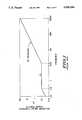
- FIG. 1illustrates the magnitude of the output frequency jitter as measured in pico-seconds, on the vertical axis, as a function of frequency, on the horizontal axis.
- the graphdemonstrates that as frequency increases, the magnitude of the allowed frequency jitter also increases, and as frequency decreases, the magnitude of the allowed frequency jitter decreases.
- a first order phase locked loop circuithas a loop filter portion with only a proportional control term. Therefore, wider noise bandwidth exists in the phase locked loop circuit, and any noise or jitter in the input reference signal is not filtered.
- a known method of reducing the frequency jitter at the output of a first order phase locked loop circuitis to control the output frequency via a number of ratioed switchable capacitors at the output of a crystal oscillator circuit. The switched capacitors are controlled directly by the output of a phase detector. In such a circuit, magnitude of the frequency jitter can be forcibly or ⁇ hard ⁇ limited to a predetermined value by limiting the maximum frequency that the oscillator can produce to the predetermined value.
- a disadvantage to conventional first order phase locked loop circuits using ratioed switched capacitors at the outputis that the frequency offset compensation of the phase locked loop is limited.
- phase locked loop having low-frequency jitter compensationhaving a phase detector implemented with digital circuitry.
- the phase detectorhas a first input for receiving a first clock signal which is a reference signal, and has a second input for receiving an output signal of the phase locked loop.
- An output of the phase detectorindicates a phase relationship between the first and second clock signals.
- a digital filter circuithas an input coupled to the output of the phase detector.
- the digital filter circuitgenerates a proportional term and an integral control term and sums the proportional control term and the integral control term to provide a digital signal.
- the digital signalrepresents a filtered output defining how to adjust the output signal of the phase locked loop circuit to maintain a predetermined output frequency.
- a digitally controlled analog oscillatoris coupled to the digital filter circuit for providing the output signal in response to the digital signal of the filter.
- FIG. 1illustrates in graphical form a graph of a conventional frequency jitter standard.
- FIG. 2illustrates in block diagram form a phase locked loop circuit in accordance with the present invention.
- Phase locked loop 10generally has a phase detector 12, a loop filter portion 13, a dither portion 16, a digitally controlled analog oscillator portion 18, and control logic 21.
- Loop filter portion 13has an integral term counter 14, a proportional term counter 20, and an adder 22.
- Dither portion 16has a decrement counter 24, a register 26, and an adder 28.
- Digitally controlled analog oscillator portion 18has an N to 2 N decoder 30, a crystal oscillator portion 32, and a switched capacitor network 34.
- Control logic 21has an input to receive an output signal of the digitally controlled analog oscillator portion 18.
- Control logic 21has a first output that is connected to a control input of proportional term counter 20, a second output that is connected to a control input of adder 22, a third output that is connected to a control input of decrement counter 24, a fourth output that is connected to a control input of register 26, a fifth output that is connected to a control input of adder 28, and a sixth output that is connected to a control input of decoder 30.
- Phase detector 12has a first input connected to a reference clock signal, and a second input for receiving an output of the digitally controlled analog oscillator portion 18. The output of the digitally controlled analog oscillator portion 18 is also the output of the phase locked loop 10.
- Phase detector 12has an output that is connected to both an input of integral term counter 14 and an input of proportional term counter 20.
- Integral term counter 14has an output that is divided into N and M-bits, where N and M are integers.
- Proportional term counter 20has a P-bit output that is connected to a first input of adder 22.
- Adder 22has second and third inputs for respectively receiving the concatenated N and an M-bit outputs of integral term counter 14, and provides an N and M-bit output.
- Decrement counter 24has an input to receive the M-bit output of adder 22, and provides a single bit output.
- Register 26has an input to receive the N-bit output of adder 22, and provides an N-bit output.
- Adder 28has a first input to receive the N-bit output of register 26, and a second input to receive the single bit output of decrement counter 24.
- Adder 28has an N-bit output that is connected to an input of decoder 30.
- Decoder 30has a 2 N bit output.
- a predetermined one of each of the 2 N bitsis connected to a control terminal of a predetermined one of a plurality of switches of the switched capacitor network 34.
- Crystal oscillator portion 32is a conventional crystal oscillator utilizing an inverter, a crystal, a resistor, and capacitors.
- Switched capacitor network 34which has an output labeled " Output,” has a plurality of equal valued capacitors. Each capacitor is coupled to one of the plurality of switches, such as capacitor 40 being coupled to switch 42.
- All of the switches within switched capacitor network 34has a first terminal connected together to form the output of switched capacitor network 34 and phase locked loop 10.
- Each switch within switched capacitor network 34has a second terminal that is each connected to a predetermined first electrode of a capacitor within the plurality of switched capacitors.
- Each switch within switched capacitor network 34has a control terminal connected to the output of decoder 30.
- a second electrode of each capacitor, within switched capacitor network 34is connected to a ground reference.
- the capacitors of switched capacitor network 34are physically distributed about crystal oscillator portion 32 to distribute the capacitance on both sides of the crystal and assist the crystal during startup operation. For convenience of illustrating the present invention, all capacitors of switched capacitor network 34 are shown only on one side of crystal oscillator portion 32.
- Phased locked loop 10provides an output frequency that is proportional to the reference frequency input. Phase locked loop 10 also minimizes the effects of frequency jitter at lower frequencies by using a dithering technique to translate low-frequency intrinsic jitter to a higher frequency jitter where the magnitude of the frequency jitter is more tolerated.
- phase detector 12which is implemented digitally, provides an output signal that is proportional to any phase difference which exists between the reference clock and the output of switched capacitor network 34.
- the digital output of phase detector 12provides a signal to loop filter portion 13 which indicates to either increase or decrease the output frequency provided by switched capacitor network 34.
- Proportional term counter 20, integral term counter 14 and adderfunction collectively to implement a loop filter which provides a digital output which further defines how to correct any phase error in the output of phase lock loop 10.
- Proportional term counter 20is implemented as a digital counter and is reset by control logic 21 at predetermined time intervals.
- Integral term counter 14is implemented as a digital up/down counter, and the decision whether to increment or decrement the counter is governed by the output from phase detector 12.
- the N-bit output of integral term counter 14represents a predetermined number of most significant bits (MSBs) from the output of the up/down count function.
- the M-bit outputs of integral term counter 14represent a predetermined upper portion of the least significant bits (LSBs) from the output of the up/down count function.
- the output of adder 22is a digital signal representing a digital sum containing control terms related to integral and proportional control of the output frequency in accordance with conventional control theory.
- the digital sum provided by adder 22is a filtered output further defining how to correct the output signal of phase locked loop 10 in a conventional manner.
- the present inventionprovides an alternative to the previously mentioned known hard limited frequency jitter first-order phase locked loop circuit by the addition of digital integral term counter 14 between phase detector 12 and the analog digitally controlled oscillator 34.
- This additionconverts the first order phase locked loop into a second order phase locked loop.
- the integral term counter 14is effectively integrating the output of phase detector 12 and filters out jitter on the reference clock without limiting the frequency-offset compensation ability of the phase locked loop.
- a loop filteralso reduces the noise bandwidth of the phase locked loop.
- the digital loop filter outputis used to adjust the frequency of the analog digitally controlled oscillator via a set of switchable capacitors at the output of the crystal oscillator portion 32.
- Each of the capacitors of switched capacitor network 34is equal valued so that network 34 is monotonic.
- the number of switchable capacitorsdetermines the number of frequency steps (frequency quantization) available, and smaller frequency quantization steps results in smaller changes in output frequency. Smaller changes in frequency at the output of the voltage controlled oscillator have the effect of reducing the magnitude of the intrinsic frequency jitter. The ability to reduce the frequency jitter is therefore dependent on the ability to manufacture small switchable capacitors. Since there is a physical limit to the size and number of ratioed switchable capacitors that can be manufactured practically on an integrated circuit, other methods of reducing frequency jitter are desired.
- the present inventionprovides a digital phase detector, a digital loop filter and an analog oscillator. This unique combination of digital and analog circuitry in a phase locked loop optimizes overall PLL performance by reducing the number and amount of external circuitry and providing accurate operation without requiring a separate high frequency clock signal in the oscillator stage.
- a dither termcan be added to the digital output of the loop filter as an additional jitter control. If the magnitude of the dither is made to vary between zero and one LSB of the control signal to the capacitor array at the output of adder 28, proportional to the LSBs of the loop filter output, the resolution of the frequency control can be improved, thereby reducing quantization effects.
- the dither termis provided by decrement counter 24, register 26, and adder 28.
- Decrement counter 24latches the M-bit digital output of adder 22 and proceeds to decrement the latched value to zero.
- the rate at which counter 24 decrementsis preferably [2 M f c ] where "f c " is a carrier frequency and is the frequency of the digital output of counter 24.
- the output of decrement counter 24is a logic one; otherwise, the output value is a logic zero.
- Register 26latches the N-bit output of adder 22, and at a predetermined time the output value of both register 26 and decrement counter 24 are presented to the input of adder 28.
- the N-bit output of adder 28provides an encoded bit pattern based on the duty cycle output of decrement counter 24 and the N-bit value latched within register 26.
- the output of adder 28has the effect of transferring the intrinsic low frequency jitter into a higher frequency jitter without increasing the magnitude of the frequency jitter. This procedure is called "dithering."
- the frequency range to which the output jitter is translatedis approximately the carrier frequency established by control logic 21. Neither the carrier frequency nor (2 M ) times the carrier frequency are particularly high frequencies. For example, as shown in FIG. 1 a carrier frequency in the range of 1 KHz allows significantly more jitter tolerance than in the one Hertz range. For this carrier frequency value, the frequency which decrement counter 24 is clocked is also not extremely high.
- decrement counter 24is clocked at 64 KHz.
- the N-bit output of adder 28is decoded into 2 N control signals by decoder 30. Each of the 2 N signals controls a predetermined switch within switched capacitor network 34 to adjust the output frequency of the crystal oscillator portion 32.
- phase locked loop circuitutilizing both a digital phase detector and loop filter, along with a digitally controlled analog oscillator to provide for an improved frequency resolution along with guaranteed monotonic frequency control and low frequency jitter compensation.
- the digital implementation of the phase detector and loop filteris less sensitive to circuit aging characteristics, variations in temperature and supply voltage, manufacturing anomalies, and is less costly as compared to various analog implementations.
- phase locked loop circuitis implemented as illustrated in FIG. 1, other ways of dithering or translating the low frequency jitter to a higher frequency jitter may be utilized.
- a specific number of capacitorsis shown in the analog digitally controlled oscillator, it should be well understood that any number of capacitors may be implemented. While a capacitor array having equal valued capacitors is shown, it should be apparent that the present invention may also be implemented with binarily weighted capacitor values.
- equal valued capacitorsguarantees monotonicity, output voltage errors may result from the switching action of the capacitors when the capacitors are not equal valued. If an output error from capacitor switching of differing voltage levels can be tolerated, then monotonicity is not required.
Landscapes
- Stabilization Of Oscillater, Synchronisation, Frequency Synthesizers (AREA)
Abstract
Description
Claims (8)
Priority Applications (2)
| Application Number | Priority Date | Filing Date | Title |
|---|---|---|---|
| US07/620,686US5036294A (en) | 1990-12-03 | 1990-12-03 | Phase locked loop having low-frequency jitter compensation |
| JP3341763AJP2929813B2 (en) | 1990-12-03 | 1991-12-02 | Phase locked loop with low frequency jitter correction |
Applications Claiming Priority (1)
| Application Number | Priority Date | Filing Date | Title |
|---|---|---|---|
| US07/620,686US5036294A (en) | 1990-12-03 | 1990-12-03 | Phase locked loop having low-frequency jitter compensation |
Publications (1)
| Publication Number | Publication Date |
|---|---|
| US5036294Atrue US5036294A (en) | 1991-07-30 |
Family
ID=24486952
Family Applications (1)
| Application Number | Title | Priority Date | Filing Date |
|---|---|---|---|
| US07/620,686Expired - LifetimeUS5036294A (en) | 1990-12-03 | 1990-12-03 | Phase locked loop having low-frequency jitter compensation |
Country Status (2)
| Country | Link |
|---|---|
| US (1) | US5036294A (en) |
| JP (1) | JP2929813B2 (en) |
Cited By (74)
| Publication number | Priority date | Publication date | Assignee | Title |
|---|---|---|---|---|
| US5241285A (en)* | 1991-10-03 | 1993-08-31 | Apogee Electronics Corporation | Phase locked loop reference slaving circuit |
| US5257293A (en)* | 1991-06-13 | 1993-10-26 | Nec Corporation | Phase locked loop for extracting clock pulses through wave differential method |
| WO1993023937A1 (en)* | 1992-05-14 | 1993-11-25 | Vlsi Technology, Inc. | Data transmission delaying circuit using time-multiplexed latch enable signals |
| US5276715A (en)* | 1990-12-21 | 1994-01-04 | Alcatel Italia Spa | Method for reducing the phase noise introduced in the resynchronization of digital signals using justification, and integrated circuits for the implementation of the method |
| EP0614275A3 (en)* | 1993-03-01 | 1994-11-17 | Codex Corp | VCO bias generator in a phase lock loop. |
| US5373255A (en)* | 1993-07-28 | 1994-12-13 | Motorola, Inc. | Low-power, jitter-compensated phase locked loop and method therefor |
| US5446420A (en)* | 1993-08-25 | 1995-08-29 | Motorola, Inc. | Method and apparatus for reducing jitter and improving testability of an oscillator |
| US5452326A (en)* | 1992-02-19 | 1995-09-19 | Sony Corporation | Digital PLL circuit with low power consumption |
| US5459680A (en)* | 1993-10-20 | 1995-10-17 | The United States Of America As Represented By The Administrator Of The National Aeronautics And Space Administration | Method and apparatus for spur-reduced digital sinusoid synthesis |
| US5475718A (en)* | 1993-02-05 | 1995-12-12 | U.S. Philips Corporation | Digital phase-locked loop |
| US5479457A (en)* | 1993-08-27 | 1995-12-26 | Vlsi Technology Inc. | Method and apparatus for attenuating jitter in a digital transmission line |
| US5528199A (en)* | 1994-12-30 | 1996-06-18 | At&T Corp. | Closed-loop frequency control of an oscillator circuit |
| US5543754A (en)* | 1994-10-11 | 1996-08-06 | National Semiconductor Corporation | Capacitor and resistor controlled oscillator timing lock loop for precision time constants |
| DE19546632A1 (en)* | 1995-12-14 | 1997-06-19 | Thomson Brandt Gmbh | Digital detector circuit in phase-locked loop for bit clock recovery |
| US5734285A (en)* | 1992-12-19 | 1998-03-31 | Harvey; Geoffrey P. | Electronic circuit utilizing resonance technique to drive clock inputs of function circuitry for saving power |
| US5787134A (en)* | 1994-09-12 | 1998-07-28 | Analog Devices, Inc. | Switched capacitance phase locked loop system |
| US6094105A (en)* | 1998-05-29 | 2000-07-25 | Intel Corporation | Oscillator with digital frequency control |
| US6104257A (en)* | 1997-12-22 | 2000-08-15 | Cypress Semiconductor Corp. | Crystal oscillator with eprom-controlled frequency trim |
| US6115439A (en)* | 1997-11-14 | 2000-09-05 | Texas Instruments Incorporated | Free running digital phase lock loop |
| US6181215B1 (en)* | 1997-09-04 | 2001-01-30 | Infineon Technologies Ag | Quartz oscillator circuit having synchronously switched frequency adjusting capacitors |
| US6194973B1 (en) | 1998-05-29 | 2001-02-27 | Intel Corporation | Oscillator with automatic gain control |
| US6246738B1 (en) | 1998-11-19 | 2001-06-12 | Pmc-Sierra Ltd. | Phase modulated reduction of clock wander in synchronous wide area networks |
| US6268776B1 (en)* | 1998-11-06 | 2001-07-31 | Kevin G. Faison | Digitally tuned and linearized low voltage crystal oscillator circuit |
| WO2001059931A1 (en)* | 2000-01-27 | 2001-08-16 | Huawei Technologies Co., Ltd. | Method for filtering used in a digital phase locked loop |
| US6300838B1 (en)* | 1999-12-22 | 2001-10-09 | International Business Machines Corporation | Method and apparatus for derivative controlled phase locked loop systems |
| US6307411B1 (en) | 2000-10-13 | 2001-10-23 | Brookhaven Science Associates | Wide tracking range, auto ranging, low jitter phase lock loop for swept and fixed frequency systems |
| DE10021273A1 (en)* | 1999-06-05 | 2001-10-31 | Inst Halbleiterphysik Gmbh | Variable inductance oscillator |
| WO2002009280A1 (en)* | 2000-07-21 | 2002-01-31 | Semiconductor Ideas To The Market (Itom) B.V. | Receiver comprising a digitally controlled capacitor bank |
| US20020044620A1 (en)* | 1999-12-17 | 2002-04-18 | Menno Spijker | Clock recovery PLL |
| US6392496B1 (en)* | 1999-06-18 | 2002-05-21 | Lg Information & Communications, Ltd. | Digital PLL circuit having a look-up table and method thereof |
| EP1255355A1 (en)* | 2001-04-26 | 2002-11-06 | Texas Instruments Incorporated | System and method for time dithering a digitally-controlled oscillator tuning input |
| US6512647B1 (en) | 1999-08-27 | 2003-01-28 | Seagate Technology Llc | Method and apparatus for adaptive tuning bias current for magnetoresistive head |
| US20030107442A1 (en)* | 2001-11-27 | 2003-06-12 | Staszewski Robert B. | All-digital frequency synthesis with capacitive re-introduction of dithered tuning information |
| US6606004B2 (en) | 2000-04-20 | 2003-08-12 | Texas Instruments Incorporated | System and method for time dithering a digitally-controlled oscillator tuning input |
| US6630868B2 (en)* | 2000-07-10 | 2003-10-07 | Silicon Laboratories, Inc. | Digitally-synthesized loop filter circuit particularly useful for a phase locked loop |
| US6686804B1 (en)* | 2001-03-19 | 2004-02-03 | Cisco Systems Wireless Networking (Australia) Pty. Limited | Frequency synthesizer using a VCO having a controllable operating point, and calibration and tuning thereof |
| US6724264B2 (en) | 1999-12-22 | 2004-04-20 | Texas Instruments Incorporated | Controller for a device with change in characteristics |
| US20040232921A1 (en)* | 2002-04-02 | 2004-11-25 | Dialog Semiconductor Gmbh | Method and circuit for compensating MOSFET capacitance variations in integrated circuits |
| US6825785B1 (en) | 2002-02-28 | 2004-11-30 | Silicon Laboratories, Inc. | Digital expander apparatus and method for generating multiple analog control signals particularly useful for controlling a sub-varactor array of a voltage controlled oscillator |
| EP1351397A3 (en)* | 2001-11-27 | 2005-03-02 | Texas Instruments Incorporated | All-digital frequency synthesis with capacitive re-introduction of dithered tuning information |
| US20050117680A1 (en)* | 2003-12-02 | 2005-06-02 | Texas Instruments Incorporated | Frequency and phase correction in a phase-locked loop (PLL) |
| DE102004007588A1 (en)* | 2004-02-17 | 2005-09-15 | Gude, Michael, Dr. | Frequency generator with variable frequency, e.g. for clock generator, continuously switches between two different frequencies to generate desired output frequency |
| US6947514B1 (en)* | 1997-06-27 | 2005-09-20 | Renesas Technology Corporation | Phase-locked loop circuit, information processing apparatus, and information processing system |
| US6973150B1 (en) | 2001-04-24 | 2005-12-06 | Rockwell Collins | Cycle slip detection using low pass filtering |
| US20060012438A1 (en)* | 2004-07-13 | 2006-01-19 | Yu-Pin Chou | Phase locked loop with nonlinear phase-error response characteristic |
| US20060050830A1 (en)* | 2004-07-30 | 2006-03-09 | Infineon Technologies Ag | Method and device for generating a clock signal |
| US20060192598A1 (en)* | 2001-06-25 | 2006-08-31 | Baird Rex T | Technique for expanding an input signal |
| US20060279365A1 (en)* | 2005-05-24 | 2006-12-14 | Andrea Camuffo | Digital phase locked loop and method for correcting interference components in a phase locked loop |
| US20070008040A1 (en)* | 2005-06-29 | 2007-01-11 | Thomas Mayer | Digital phase locked loop, method for controlling a digital phase locked loop and method for generating an oscillator signal |
| US20070176691A1 (en)* | 2006-01-30 | 2007-08-02 | Batchelor Jeffrey S | Expanded pull range for a voltage controlled clock synthesizer |
| US20070200638A1 (en)* | 2006-01-19 | 2007-08-30 | Texas Instruments Deutschland Gmbh | All digital phase locked loop system and method |
| US20070222527A1 (en)* | 2005-12-20 | 2007-09-27 | Harald Pretl | Frequency tuning circuit, use of the tuning circuit and method for frequency tuning |
| US20090167399A1 (en)* | 2007-12-31 | 2009-07-02 | Industrial Technology Research Institute | Signal delay circuit |
| US20100073054A1 (en)* | 2008-09-19 | 2010-03-25 | Altera Corporation | Techniques For Digital Loop Filters |
| US7701297B1 (en) | 2005-06-30 | 2010-04-20 | Cypress Semiconductor Corporation | Spread spectrum frequency synthesizer with improved frequency shape by adjusting the length of a standard curve used for spread spectrum modulation |
| US7741918B1 (en) | 2005-06-30 | 2010-06-22 | Cypress Semiconductor Corporation | System and method for an enhanced noise shaping for spread spectrum modulation |
| US20100188158A1 (en)* | 2009-01-23 | 2010-07-29 | Ainspan Herschel A | Optimal dithering of a digitally controlled oscillator with clock dithering for gain and bandwidth control |
| US7813411B1 (en) | 2005-06-30 | 2010-10-12 | Cypress Semiconductor Corporation | Spread spectrum frequency synthesizer with high order accumulation for frequency profile generation |
| US20100323643A1 (en)* | 2008-02-28 | 2010-12-23 | Nxp B.V. | Frequency synthesis |
| US7912109B1 (en) | 2005-06-30 | 2011-03-22 | Cypress Semiconductor Corporation | Spread spectrum frequency synthesizer with first order accumulation for frequency profile generation |
| US7932787B1 (en) | 2005-06-30 | 2011-04-26 | Cypress Semiconductor Corporation | Phase lock loop control system and method |
| US7948327B1 (en) | 2005-06-30 | 2011-05-24 | Cypress Semiconductor Corporation | Simplified phase lock loop control model system and method |
| US7961059B1 (en) | 2005-06-30 | 2011-06-14 | Cypress Semiconductor Corporation | Phase lock loop control system and method with non-consecutive feedback divide values |
| US20110182389A1 (en)* | 2007-11-16 | 2011-07-28 | St-Ericsson Sa | Jitter compensation |
| US8035455B1 (en) | 2005-12-21 | 2011-10-11 | Cypress Semiconductor Corporation | Oscillator amplitude control network |
| US8072277B1 (en) | 2005-06-30 | 2011-12-06 | Cypress Semiconductor Corporation | Spread spectrum frequency synthesizer |
| US8174326B1 (en) | 2005-06-30 | 2012-05-08 | Cypress Semiconductor Corporation | Phase lock loop control error selection system and method |
| TWI392221B (en)* | 2005-05-24 | 2013-04-01 | Axiom Microdevices Inc | A method for modulating phase or frequency in a communication system using clock division |
| US8698567B2 (en)* | 2012-04-02 | 2014-04-15 | Avago Technologies General Ip (Singapore) Pte. Ltd. | Phase-locked loop calibration system and method |
| EP3217555A1 (en)* | 2016-03-07 | 2017-09-13 | Nxp B.V. | Data conversion |
| TWI663837B (en)* | 2018-03-13 | 2019-06-21 | 群聯電子股份有限公司 | Phase-locked loop circuit calibration method, memory storage device and connection interface circuit |
| US10623006B2 (en) | 2017-06-28 | 2020-04-14 | Analog Devices, Inc. | Apparatus and methods for compensation of signal path delay variation |
| US11038511B2 (en) | 2017-06-28 | 2021-06-15 | Analog Devices International Unlimited Company | Apparatus and methods for system clock compensation |
| RU2765273C1 (en)* | 2021-07-01 | 2022-01-27 | Акционерное общество "Концерн "Созвездие" | Low distortion frequency modulated digital signal conditioner |
Families Citing this family (2)
| Publication number | Priority date | Publication date | Assignee | Title |
|---|---|---|---|---|
| JP2005204091A (en)* | 2004-01-16 | 2005-07-28 | Daihen Corp | Pll circuit |
| US9485085B2 (en)* | 2015-03-10 | 2016-11-01 | Qualcomm Incorporated | Phase locked loop (PLL) architecture |
Citations (3)
| Publication number | Priority date | Publication date | Assignee | Title |
|---|---|---|---|---|
| US4941156A (en)* | 1987-05-19 | 1990-07-10 | Crystal Semiconductor | Linear jitter attenuator |
| US4942371A (en)* | 1988-08-31 | 1990-07-17 | Nec Corporation | Phase-locked loop having improved input jitter characteristics |
| US4942370A (en)* | 1988-04-08 | 1990-07-17 | Ricoh Company, Ltd. | PLL circuit with band width varying in accordance with the frequency of an input signal |
- 1990
- 1990-12-03USUS07/620,686patent/US5036294A/ennot_activeExpired - Lifetime
- 1991
- 1991-12-02JPJP3341763Apatent/JP2929813B2/ennot_activeExpired - Fee Related
Patent Citations (3)
| Publication number | Priority date | Publication date | Assignee | Title |
|---|---|---|---|---|
| US4941156A (en)* | 1987-05-19 | 1990-07-10 | Crystal Semiconductor | Linear jitter attenuator |
| US4942370A (en)* | 1988-04-08 | 1990-07-17 | Ricoh Company, Ltd. | PLL circuit with band width varying in accordance with the frequency of an input signal |
| US4942371A (en)* | 1988-08-31 | 1990-07-17 | Nec Corporation | Phase-locked loop having improved input jitter characteristics |
Cited By (122)
| Publication number | Priority date | Publication date | Assignee | Title |
|---|---|---|---|---|
| US5276715A (en)* | 1990-12-21 | 1994-01-04 | Alcatel Italia Spa | Method for reducing the phase noise introduced in the resynchronization of digital signals using justification, and integrated circuits for the implementation of the method |
| AU646375B2 (en)* | 1991-06-13 | 1994-02-17 | Nec Corporation | Phase locked loop for extracting clock pulses through wave differential method |
| US5257293A (en)* | 1991-06-13 | 1993-10-26 | Nec Corporation | Phase locked loop for extracting clock pulses through wave differential method |
| US5241285A (en)* | 1991-10-03 | 1993-08-31 | Apogee Electronics Corporation | Phase locked loop reference slaving circuit |
| US5452326A (en)* | 1992-02-19 | 1995-09-19 | Sony Corporation | Digital PLL circuit with low power consumption |
| WO1993023937A1 (en)* | 1992-05-14 | 1993-11-25 | Vlsi Technology, Inc. | Data transmission delaying circuit using time-multiplexed latch enable signals |
| US5734285A (en)* | 1992-12-19 | 1998-03-31 | Harvey; Geoffrey P. | Electronic circuit utilizing resonance technique to drive clock inputs of function circuitry for saving power |
| US5475718A (en)* | 1993-02-05 | 1995-12-12 | U.S. Philips Corporation | Digital phase-locked loop |
| EP0614275A3 (en)* | 1993-03-01 | 1994-11-17 | Codex Corp | VCO bias generator in a phase lock loop. |
| US5373255A (en)* | 1993-07-28 | 1994-12-13 | Motorola, Inc. | Low-power, jitter-compensated phase locked loop and method therefor |
| EP0637137A3 (en)* | 1993-07-28 | 1996-07-03 | Motorola Inc | Low-power, jitter-compensated phase locked loop and method therefor. |
| US5446420A (en)* | 1993-08-25 | 1995-08-29 | Motorola, Inc. | Method and apparatus for reducing jitter and improving testability of an oscillator |
| US5511126A (en)* | 1993-08-25 | 1996-04-23 | Motorola, Inc. | Method and apparatus for reducing jitter and improving testability of an oscillator |
| EP0641080A3 (en)* | 1993-08-25 | 1996-06-12 | Motorola Inc | Method and apparatus for reducing jitter and improving testability of an oscillator. |
| US5479457A (en)* | 1993-08-27 | 1995-12-26 | Vlsi Technology Inc. | Method and apparatus for attenuating jitter in a digital transmission line |
| US5982833A (en)* | 1993-08-27 | 1999-11-09 | Vlsi Technology, Inc. | Method and apparatus for attenuating jitter in a digital transmission line |
| US5546432A (en)* | 1993-08-27 | 1996-08-13 | Vlsi Technology, Inc. | Method and apparatus for attenuating jitter in a digital transmission line |
| US5550877A (en)* | 1993-08-27 | 1996-08-27 | Vlsi Technology, Inc. | Method and apparatus for attenuating jitter in a digital transmission line |
| US5459680A (en)* | 1993-10-20 | 1995-10-17 | The United States Of America As Represented By The Administrator Of The National Aeronautics And Space Administration | Method and apparatus for spur-reduced digital sinusoid synthesis |
| US5787134A (en)* | 1994-09-12 | 1998-07-28 | Analog Devices, Inc. | Switched capacitance phase locked loop system |
| US5543754A (en)* | 1994-10-11 | 1996-08-06 | National Semiconductor Corporation | Capacitor and resistor controlled oscillator timing lock loop for precision time constants |
| EP0720299A1 (en)* | 1994-12-30 | 1996-07-03 | AT&T Corp. | Closed-loop frequency control of an oscillator circuit |
| US5528199A (en)* | 1994-12-30 | 1996-06-18 | At&T Corp. | Closed-loop frequency control of an oscillator circuit |
| DE19546632A1 (en)* | 1995-12-14 | 1997-06-19 | Thomson Brandt Gmbh | Digital detector circuit in phase-locked loop for bit clock recovery |
| US5946363A (en)* | 1995-12-14 | 1999-08-31 | Deutsche Thomson-Brandt Gmbh | Digital detector circuit for recovering the bit timing from a data stream |
| US6947514B1 (en)* | 1997-06-27 | 2005-09-20 | Renesas Technology Corporation | Phase-locked loop circuit, information processing apparatus, and information processing system |
| US6181215B1 (en)* | 1997-09-04 | 2001-01-30 | Infineon Technologies Ag | Quartz oscillator circuit having synchronously switched frequency adjusting capacitors |
| US6115439A (en)* | 1997-11-14 | 2000-09-05 | Texas Instruments Incorporated | Free running digital phase lock loop |
| US6104257A (en)* | 1997-12-22 | 2000-08-15 | Cypress Semiconductor Corp. | Crystal oscillator with eprom-controlled frequency trim |
| US6285264B1 (en) | 1997-12-22 | 2001-09-04 | Cypress Semiconductor Corp. | Crystal oscillator with frequency trim |
| US6194973B1 (en) | 1998-05-29 | 2001-02-27 | Intel Corporation | Oscillator with automatic gain control |
| US6094105A (en)* | 1998-05-29 | 2000-07-25 | Intel Corporation | Oscillator with digital frequency control |
| US6268776B1 (en)* | 1998-11-06 | 2001-07-31 | Kevin G. Faison | Digitally tuned and linearized low voltage crystal oscillator circuit |
| US6246738B1 (en) | 1998-11-19 | 2001-06-12 | Pmc-Sierra Ltd. | Phase modulated reduction of clock wander in synchronous wide area networks |
| US6861913B1 (en) | 1999-06-05 | 2005-03-01 | Ihp Gmbh - Innovations For High Performance Microelectronics | Voltage-controlled oscillator with LC resonant circuit |
| DE10021273A1 (en)* | 1999-06-05 | 2001-10-31 | Inst Halbleiterphysik Gmbh | Variable inductance oscillator |
| US6392496B1 (en)* | 1999-06-18 | 2002-05-21 | Lg Information & Communications, Ltd. | Digital PLL circuit having a look-up table and method thereof |
| US6512647B1 (en) | 1999-08-27 | 2003-01-28 | Seagate Technology Llc | Method and apparatus for adaptive tuning bias current for magnetoresistive head |
| US6959064B2 (en)* | 1999-12-17 | 2005-10-25 | Zarlink Semiconductor Inc. | Clock recovery PLL |
| US20020044620A1 (en)* | 1999-12-17 | 2002-04-18 | Menno Spijker | Clock recovery PLL |
| US6300838B1 (en)* | 1999-12-22 | 2001-10-09 | International Business Machines Corporation | Method and apparatus for derivative controlled phase locked loop systems |
| US6724264B2 (en) | 1999-12-22 | 2004-04-20 | Texas Instruments Incorporated | Controller for a device with change in characteristics |
| WO2001059931A1 (en)* | 2000-01-27 | 2001-08-16 | Huawei Technologies Co., Ltd. | Method for filtering used in a digital phase locked loop |
| US6606004B2 (en) | 2000-04-20 | 2003-08-12 | Texas Instruments Incorporated | System and method for time dithering a digitally-controlled oscillator tuning input |
| US6630868B2 (en)* | 2000-07-10 | 2003-10-07 | Silicon Laboratories, Inc. | Digitally-synthesized loop filter circuit particularly useful for a phase locked loop |
| US20040263225A1 (en)* | 2000-07-10 | 2004-12-30 | Perrott Michael H. | Digitally-synthesized loop filter method and circuit particularly useful for a phase locked loop |
| US20040051590A1 (en)* | 2000-07-10 | 2004-03-18 | Silicon Laboratories, Inc. | Digitally-synthesized loop filter circuit particularly useful for a phase locked loop |
| US6765445B2 (en) | 2000-07-10 | 2004-07-20 | Silicon Laboratories, Inc. | Digitally-synthesized loop filter circuit particularly useful for a phase locked loop |
| US7613267B2 (en) | 2000-07-10 | 2009-11-03 | Silicon Laboratories Inc. | Digitally-synthesized loop filter method and circuit particularly useful for a phase locked loop |
| KR100767166B1 (en)* | 2000-07-21 | 2007-10-15 | 세미컨덕터 아이디어스 투 더 마켓트(아이톰) 비.브이. | Receiver with digitally controlled capacitor bank |
| WO2002009280A1 (en)* | 2000-07-21 | 2002-01-31 | Semiconductor Ideas To The Market (Itom) B.V. | Receiver comprising a digitally controlled capacitor bank |
| EP1182778A1 (en)* | 2000-07-21 | 2002-02-27 | Semiconductor Ideas to The Market (ItoM) BV | Receiver comprising a digitally controlled capacitor bank |
| US6307411B1 (en) | 2000-10-13 | 2001-10-23 | Brookhaven Science Associates | Wide tracking range, auto ranging, low jitter phase lock loop for swept and fixed frequency systems |
| US6686804B1 (en)* | 2001-03-19 | 2004-02-03 | Cisco Systems Wireless Networking (Australia) Pty. Limited | Frequency synthesizer using a VCO having a controllable operating point, and calibration and tuning thereof |
| US6973150B1 (en) | 2001-04-24 | 2005-12-06 | Rockwell Collins | Cycle slip detection using low pass filtering |
| EP1255355A1 (en)* | 2001-04-26 | 2002-11-06 | Texas Instruments Incorporated | System and method for time dithering a digitally-controlled oscillator tuning input |
| US7679455B2 (en) | 2001-06-25 | 2010-03-16 | Silicon Laboratories Inc. | Technique for expanding an input signal |
| US7133485B1 (en) | 2001-06-25 | 2006-11-07 | Silicon Laboratories Inc. | Feedback system incorporating slow digital switching for glitch-free state changes |
| US20060192598A1 (en)* | 2001-06-25 | 2006-08-31 | Baird Rex T | Technique for expanding an input signal |
| US7463098B2 (en) | 2001-06-25 | 2008-12-09 | Silicon Laboratories Inc. | Feedback system incorporating slow digital switching for glitch-free state changes |
| EP1351397A3 (en)* | 2001-11-27 | 2005-03-02 | Texas Instruments Incorporated | All-digital frequency synthesis with capacitive re-introduction of dithered tuning information |
| US7046098B2 (en) | 2001-11-27 | 2006-05-16 | Texas Instruments Incorporated | All-digital frequency synthesis with capacitive re-introduction of dithered tuning information |
| US20030107442A1 (en)* | 2001-11-27 | 2003-06-12 | Staszewski Robert B. | All-digital frequency synthesis with capacitive re-introduction of dithered tuning information |
| US20050134491A1 (en)* | 2002-02-28 | 2005-06-23 | Yunteng Huang | Digital expander apparatus and method for generating multiple analog control signals particularly useful for controlling an oscillator |
| US7262725B2 (en) | 2002-02-28 | 2007-08-28 | Silicon Laboratories, Inc. | Digital expander for generating multiple analog control signals particularly useful for controlling an oscillator |
| US7084710B2 (en) | 2002-02-28 | 2006-08-01 | Silicon Laboratories Inc. | Digital expander apparatus and method for generating multiple analog control signals particularly useful for controlling an oscillator |
| US20060284746A1 (en)* | 2002-02-28 | 2006-12-21 | Yunteng Huang | Digital expander for generating multiple analog control signals particularly useful for controlling an oscillator |
| US6825785B1 (en) | 2002-02-28 | 2004-11-30 | Silicon Laboratories, Inc. | Digital expander apparatus and method for generating multiple analog control signals particularly useful for controlling a sub-varactor array of a voltage controlled oscillator |
| US7002421B2 (en)* | 2002-04-02 | 2006-02-21 | Dialog Semiconductor Gmbh | Method and circuit for compensating MOSFET capacitance variations in integrated circuits |
| US20040232921A1 (en)* | 2002-04-02 | 2004-11-25 | Dialog Semiconductor Gmbh | Method and circuit for compensating MOSFET capacitance variations in integrated circuits |
| US7277519B2 (en) | 2003-12-02 | 2007-10-02 | Texas Instruments Incorporated | Frequency and phase correction in a phase-locked loop (PLL) |
| US20050117680A1 (en)* | 2003-12-02 | 2005-06-02 | Texas Instruments Incorporated | Frequency and phase correction in a phase-locked loop (PLL) |
| EP1538754A1 (en)* | 2003-12-02 | 2005-06-08 | Texas Instruments Incorporated | Frequency and phase correction in a phase-locked loop |
| DE102004007588B4 (en)* | 2004-02-17 | 2016-01-21 | Michael Gude | Frequency generator with digitally adjustable frequency |
| DE102004007588A1 (en)* | 2004-02-17 | 2005-09-15 | Gude, Michael, Dr. | Frequency generator with variable frequency, e.g. for clock generator, continuously switches between two different frequencies to generate desired output frequency |
| US20060012438A1 (en)* | 2004-07-13 | 2006-01-19 | Yu-Pin Chou | Phase locked loop with nonlinear phase-error response characteristic |
| US7218177B2 (en)* | 2004-07-13 | 2007-05-15 | Realtek Semiconductor Corp. | Phase locked loop with nonlinear phase-error response characteristic |
| US7282999B2 (en) | 2004-07-30 | 2007-10-16 | Infineon Technologies Ag | Method and device for generating a clock signal using a phase difference signal and a feedback signal |
| US20060050830A1 (en)* | 2004-07-30 | 2006-03-09 | Infineon Technologies Ag | Method and device for generating a clock signal |
| DE102004037162A1 (en)* | 2004-07-30 | 2006-03-23 | Infineon Technologies Ag | Method and device for generating a clock signal |
| TWI392221B (en)* | 2005-05-24 | 2013-04-01 | Axiom Microdevices Inc | A method for modulating phase or frequency in a communication system using clock division |
| US7724094B2 (en)* | 2005-05-24 | 2010-05-25 | Infineon Technologies Ag | Digital phase locked loop and method for correcting interference components in a phase locked loop |
| US20060279365A1 (en)* | 2005-05-24 | 2006-12-14 | Andrea Camuffo | Digital phase locked loop and method for correcting interference components in a phase locked loop |
| DE102005030356B4 (en)* | 2005-06-29 | 2011-07-07 | Infineon Technologies AG, 81669 | Digital phase locked loop and method for controlling a digital phase locked loop |
| US20070008040A1 (en)* | 2005-06-29 | 2007-01-11 | Thomas Mayer | Digital phase locked loop, method for controlling a digital phase locked loop and method for generating an oscillator signal |
| US8072277B1 (en) | 2005-06-30 | 2011-12-06 | Cypress Semiconductor Corporation | Spread spectrum frequency synthesizer |
| US7948327B1 (en) | 2005-06-30 | 2011-05-24 | Cypress Semiconductor Corporation | Simplified phase lock loop control model system and method |
| US7701297B1 (en) | 2005-06-30 | 2010-04-20 | Cypress Semiconductor Corporation | Spread spectrum frequency synthesizer with improved frequency shape by adjusting the length of a standard curve used for spread spectrum modulation |
| US8174326B1 (en) | 2005-06-30 | 2012-05-08 | Cypress Semiconductor Corporation | Phase lock loop control error selection system and method |
| US7741918B1 (en) | 2005-06-30 | 2010-06-22 | Cypress Semiconductor Corporation | System and method for an enhanced noise shaping for spread spectrum modulation |
| US7813411B1 (en) | 2005-06-30 | 2010-10-12 | Cypress Semiconductor Corporation | Spread spectrum frequency synthesizer with high order accumulation for frequency profile generation |
| US7961059B1 (en) | 2005-06-30 | 2011-06-14 | Cypress Semiconductor Corporation | Phase lock loop control system and method with non-consecutive feedback divide values |
| US7912109B1 (en) | 2005-06-30 | 2011-03-22 | Cypress Semiconductor Corporation | Spread spectrum frequency synthesizer with first order accumulation for frequency profile generation |
| US7932787B1 (en) | 2005-06-30 | 2011-04-26 | Cypress Semiconductor Corporation | Phase lock loop control system and method |
| US20070222527A1 (en)* | 2005-12-20 | 2007-09-27 | Harald Pretl | Frequency tuning circuit, use of the tuning circuit and method for frequency tuning |
| US7847642B2 (en)* | 2005-12-20 | 2010-12-07 | Infineon Technologies Ag | Frequency tuning circuit, use of the tuning circuit and method for frequency tuning |
| US8035455B1 (en) | 2005-12-21 | 2011-10-11 | Cypress Semiconductor Corporation | Oscillator amplitude control network |
| US7605664B2 (en)* | 2006-01-19 | 2009-10-20 | Texas Instruments Deutschland Gmbh | All digital phase locked loop system and method |
| US20070200638A1 (en)* | 2006-01-19 | 2007-08-30 | Texas Instruments Deutschland Gmbh | All digital phase locked loop system and method |
| US20070176691A1 (en)* | 2006-01-30 | 2007-08-02 | Batchelor Jeffrey S | Expanded pull range for a voltage controlled clock synthesizer |
| US7342460B2 (en) | 2006-01-30 | 2008-03-11 | Silicon Laboratories Inc. | Expanded pull range for a voltage controlled clock synthesizer |
| US8594253B2 (en)* | 2007-11-16 | 2013-11-26 | St-Ericsson Sa | Jitter compensation |
| US20110182389A1 (en)* | 2007-11-16 | 2011-07-28 | St-Ericsson Sa | Jitter compensation |
| US7977993B2 (en) | 2007-12-31 | 2011-07-12 | Industrial Technology Research Institute | Signal delay circuit |
| US20090167399A1 (en)* | 2007-12-31 | 2009-07-02 | Industrial Technology Research Institute | Signal delay circuit |
| US20100323643A1 (en)* | 2008-02-28 | 2010-12-23 | Nxp B.V. | Frequency synthesis |
| US20100073054A1 (en)* | 2008-09-19 | 2010-03-25 | Altera Corporation | Techniques For Digital Loop Filters |
| US8212610B2 (en) | 2008-09-19 | 2012-07-03 | Altera Corporation | Techniques for digital loop filters |
| US8138840B2 (en) | 2009-01-23 | 2012-03-20 | International Business Machines Corporation | Optimal dithering of a digitally controlled oscillator with clock dithering for gain and bandwidth control |
| US20100188158A1 (en)* | 2009-01-23 | 2010-07-29 | Ainspan Herschel A | Optimal dithering of a digitally controlled oscillator with clock dithering for gain and bandwidth control |
| US8698567B2 (en)* | 2012-04-02 | 2014-04-15 | Avago Technologies General Ip (Singapore) Pte. Ltd. | Phase-locked loop calibration system and method |
| EP3217555A1 (en)* | 2016-03-07 | 2017-09-13 | Nxp B.V. | Data conversion |
| US11177816B2 (en) | 2017-06-28 | 2021-11-16 | Analog Devices, Inc. | Fast locking sequence for phase-locked loops |
| US10623006B2 (en) | 2017-06-28 | 2020-04-14 | Analog Devices, Inc. | Apparatus and methods for compensation of signal path delay variation |
| US10749535B2 (en) | 2017-06-28 | 2020-08-18 | Analog Devices, Inc. | Apparatus and methods for distributed timing using digital time stamps from a time-to-digital converter |
| US10749534B2 (en) | 2017-06-28 | 2020-08-18 | Analog Devices, Inc. | Apparatus and methods for system clock compensation |
| US10848161B2 (en) | 2017-06-28 | 2020-11-24 | Analog Devices, Inc. | Reference monitors with dynamically controlled latency |
| US11038511B2 (en) | 2017-06-28 | 2021-06-15 | Analog Devices International Unlimited Company | Apparatus and methods for system clock compensation |
| US11705914B2 (en) | 2017-06-28 | 2023-07-18 | Analog Devices, Inc. | Phase detectors with alignment to phase information lost in decimation |
| US12212328B2 (en) | 2017-06-28 | 2025-01-28 | Analog Devices, Inc. | Phase detectors with extrapolation of timing events |
| TWI663837B (en)* | 2018-03-13 | 2019-06-21 | 群聯電子股份有限公司 | Phase-locked loop circuit calibration method, memory storage device and connection interface circuit |
| RU2765273C1 (en)* | 2021-07-01 | 2022-01-27 | Акционерное общество "Концерн "Созвездие" | Low distortion frequency modulated digital signal conditioner |
Also Published As
| Publication number | Publication date |
|---|---|
| JPH04307815A (en) | 1992-10-30 |
| JP2929813B2 (en) | 1999-08-03 |
Similar Documents
| Publication | Publication Date | Title |
|---|---|---|
| US5036294A (en) | Phase locked loop having low-frequency jitter compensation | |
| US6646581B1 (en) | Digital-to-analog converter circuit incorporating hybrid sigma-delta modulator circuit | |
| US7084710B2 (en) | Digital expander apparatus and method for generating multiple analog control signals particularly useful for controlling an oscillator | |
| US5604468A (en) | Frequency synthesizer with temperature compensation and frequency multiplication and method of providing the same | |
| CN111327313B (en) | Apparatus for digitally controlled oscillators and related methods | |
| US7924193B2 (en) | All-digital spread spectrum clock generator | |
| US8509371B2 (en) | Continuous-rate clock recovery circuit | |
| US6329859B1 (en) | N-way circular phase interpolator for generating a signal having arbitrary phase | |
| US7898343B1 (en) | Frequency-locked loop calibration of a phase-locked loop gain | |
| US5130671A (en) | Phase-locked loop frequency tracking device including a direct digital synthesizer | |
| US4810977A (en) | Frequency modulation in phase-locked loops | |
| US5349309A (en) | Second order phase locked loop | |
| US20020136342A1 (en) | Sample and hold type fractional-N frequency synthesezer | |
| US20140354336A1 (en) | Digital PLL With Hybrid Phase/Frequency Detector and Digital Noise Cancellation | |
| US20100231310A1 (en) | Mixed-mode pll | |
| EP1547249B1 (en) | Voltage-controlled oscillator presetting circuit | |
| US5184092A (en) | Phase-locked loop frequency tracking device including a direct digital synthesizer | |
| US11437980B2 (en) | Frequency to digital converter, asynchronous phase sampler and digitally controlled oscillator methods | |
| EP0557799B1 (en) | Digital error corrected fractional-N synthesizer | |
| US20120139654A1 (en) | Frequency synthesizer | |
| US6714084B2 (en) | High resolution digital controlled oscillator | |
| US6693987B1 (en) | Digital-to-analog DAC-driven phase-locked loop PLL with slave PLL's driving DAC reference voltages | |
| US7308062B2 (en) | Apparatus for providing system clock synchronized to a network universally | |
| JPH0993125A (en) | Pll synthesizer circuit | |
| KR100739998B1 (en) | Phase locked loop with automatic compensation of voltage controlled oscillator |
Legal Events
| Date | Code | Title | Description |
|---|---|---|---|
| AS | Assignment | Owner name:MOTOROLA, INC., SCHAUMBURG, IL A CORP. OF DE Free format text:ASSIGNMENT OF ASSIGNORS INTEREST.;ASSIGNOR:MCCASLIN, SHAWN ROBERT;REEL/FRAME:005528/0406 Effective date:19901127 | |
| STCF | Information on status: patent grant | Free format text:PATENTED CASE | |
| FEPP | Fee payment procedure | Free format text:PAYOR NUMBER ASSIGNED (ORIGINAL EVENT CODE: ASPN); ENTITY STATUS OF PATENT OWNER: LARGE ENTITY | |
| FPAY | Fee payment | Year of fee payment:4 | |
| FPAY | Fee payment | Year of fee payment:8 | |
| FPAY | Fee payment | Year of fee payment:12 | |
| AS | Assignment | Owner name:FREESCALE SEMICONDUCTOR, INC., TEXAS Free format text:ASSIGNMENT OF ASSIGNORS INTEREST;ASSIGNOR:MOTOROLA, INC.;REEL/FRAME:015698/0657 Effective date:20040404 Owner name:FREESCALE SEMICONDUCTOR, INC.,TEXAS Free format text:ASSIGNMENT OF ASSIGNORS INTEREST;ASSIGNOR:MOTOROLA, INC.;REEL/FRAME:015698/0657 Effective date:20040404 | |
| AS | Assignment | Owner name:CITIBANK, N.A. AS COLLATERAL AGENT, NEW YORK Free format text:SECURITY AGREEMENT;ASSIGNORS:FREESCALE SEMICONDUCTOR, INC.;FREESCALE ACQUISITION CORPORATION;FREESCALE ACQUISITION HOLDINGS CORP.;AND OTHERS;REEL/FRAME:018855/0129 Effective date:20061201 Owner name:CITIBANK, N.A. AS COLLATERAL AGENT,NEW YORK Free format text:SECURITY AGREEMENT;ASSIGNORS:FREESCALE SEMICONDUCTOR, INC.;FREESCALE ACQUISITION CORPORATION;FREESCALE ACQUISITION HOLDINGS CORP.;AND OTHERS;REEL/FRAME:018855/0129 Effective date:20061201 | |
| AS | Assignment | Owner name:CITIBANK, N.A., AS COLLATERAL AGENT,NEW YORK Free format text:SECURITY AGREEMENT;ASSIGNOR:FREESCALE SEMICONDUCTOR, INC.;REEL/FRAME:024397/0001 Effective date:20100413 Owner name:CITIBANK, N.A., AS COLLATERAL AGENT, NEW YORK Free format text:SECURITY AGREEMENT;ASSIGNOR:FREESCALE SEMICONDUCTOR, INC.;REEL/FRAME:024397/0001 Effective date:20100413 | |
| AS | Assignment | Owner name:FREESCALE SEMICONDUCTOR, INC., TEXAS Free format text:PATENT RELEASE;ASSIGNOR:CITIBANK, N.A., AS COLLATERAL AGENT;REEL/FRAME:037354/0225 Effective date:20151207 Owner name:FREESCALE SEMICONDUCTOR, INC., TEXAS Free format text:PATENT RELEASE;ASSIGNOR:CITIBANK, N.A., AS COLLATERAL AGENT;REEL/FRAME:037356/0553 Effective date:20151207 Owner name:FREESCALE SEMICONDUCTOR, INC., TEXAS Free format text:PATENT RELEASE;ASSIGNOR:CITIBANK, N.A., AS COLLATERAL AGENT;REEL/FRAME:037356/0143 Effective date:20151207 |