US5034917A - Computer system including a page mode memory with decreased access time and method of operation thereof - Google Patents
Computer system including a page mode memory with decreased access time and method of operation thereofDownload PDFInfo
- Publication number
- US5034917A US5034917AUS07/196,721US19672188AUS5034917AUS 5034917 AUS5034917 AUS 5034917AUS 19672188 AUS19672188 AUS 19672188AUS 5034917 AUS5034917 AUS 5034917A
- Authority
- US
- United States
- Prior art keywords
- memory
- data
- address
- bus
- cycle
- Prior art date
- Legal status (The legal status is an assumption and is not a legal conclusion. Google has not performed a legal analysis and makes no representation as to the accuracy of the status listed.)
- Expired - Fee Related
Links
Images


Classifications
- G—PHYSICS
- G06—COMPUTING OR CALCULATING; COUNTING
- G06F—ELECTRIC DIGITAL DATA PROCESSING
- G06F12/00—Accessing, addressing or allocating within memory systems or architectures
- G06F12/02—Addressing or allocation; Relocation
- G06F12/06—Addressing a physical block of locations, e.g. base addressing, module addressing, memory dedication
- G—PHYSICS
- G11—INFORMATION STORAGE
- G11C—STATIC STORES
- G11C7/00—Arrangements for writing information into, or reading information out from, a digital store
- G11C7/10—Input/output [I/O] data interface arrangements, e.g. I/O data control circuits, I/O data buffers
- G11C7/1015—Read-write modes for single port memories, i.e. having either a random port or a serial port
- G11C7/1018—Serial bit line access mode, e.g. using bit line address shift registers, bit line address counters, bit line burst counters
- G11C7/1021—Page serial bit line access mode, i.e. using an enabled row address stroke pulse with its associated word line address and a sequence of enabled column address stroke pulses each with its associated bit line address
- G—PHYSICS
- G06—COMPUTING OR CALCULATING; COUNTING
- G06F—ELECTRIC DIGITAL DATA PROCESSING
- G06F13/00—Interconnection of, or transfer of information or other signals between, memories, input/output devices or central processing units
- G06F13/14—Handling requests for interconnection or transfer
- G06F13/36—Handling requests for interconnection or transfer for access to common bus or bus system
- G06F13/362—Handling requests for interconnection or transfer for access to common bus or bus system with centralised access control
- G—PHYSICS
- G06—COMPUTING OR CALCULATING; COUNTING
- G06F—ELECTRIC DIGITAL DATA PROCESSING
- G06F8/00—Arrangements for software engineering
- G06F8/20—Software design
- G—PHYSICS
- G06—COMPUTING OR CALCULATING; COUNTING
- G06F—ELECTRIC DIGITAL DATA PROCESSING
- G06F8/00—Arrangements for software engineering
- G06F8/70—Software maintenance or management
- G06F8/71—Version control; Configuration management
Definitions
- This inventionrelates in general to memories employed in computer systems and, more particularly, to accessing data stored in page mode memories employed in such systems.
- page mode memorymemory is divided into a plurality of pages, each page consisting of a row having a common row address for the entire row.
- Each row of a pageincludes a plurality of columns having corresponding column addresses.
- the row address of that datais supplied to the memory to enable selection of the page in memory where the data is located.
- the column address associated with the datais supplied to the memory to enable selection of the particular piece of data within the addressed row or page.
- the addressed datais then read out to the data bus.
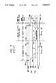
- System 10includes a central processing unit (CPU) 20 or microprocessor to which an address bus 30 and a data bus 40 are coupled.
- System 10further includes a memory controller 50 to which address bus 30 and data bus 40 are coupled.
- a control bus 60is coupled between CPU 20 and memory controller 50 such that control signals may be passed therebetween.
- Memory controller 50is coupled to at least one memory module 70 which consists of random access memory (RAM).
- RAMrandom access memory
- memory module 70is divided into pages which are 2K bytes long (512 ⁇ 32 plus parity), each page by definition having the same row address. Each page thus includes 2K column addresses.
- a data bus 80is coupled between memory controller 50 and memory module 70 to permit the transfer of data therebetween.
- a multiplexed MUX address bus 90is coupled between memory controller 50 and memory module 70 so that row and column address information may be passed from memory controller 50 to memory module 70.
- Multiplexed address bus 90has fewer lines than address bus 30 due to the multiplex nature of bus 90 on which a row or page address is first supplied to memory module 90 during a memory access cycle and then, second, a column address is supplied to memory module 90 later in that cycle.
- Memory controller 50supplies Row Address Strobe (RAS) signals and Column Address Strobe (CAS) signals to memory module 70 as seen in FIG. 1. The nature of the RAS and CAS signals is described in the following discussion of the timing diagram of FIG. 2.
- FIG. 2shows a timing diagram of a typical memory cycle associated with computer system 10.
- CPU 20desires to access or retrieve a first piece of data from memory 70 at a predetermined data address therein.
- CPU 20sends the data address to memory controller 50.
- Memory controller 50effectively divides the data address into two portions, namely, the row address (also known as the page address) and the column address.
- the row address and the column addressare multiplexed onto MUX ADDRESS bus 90. That is, the row address is first provided to such MUX ADDRESS bus at 100.
- the RAS signalis initially HIGH or OFF. It is noted that since negative logic is employed in the timing diagram of FIG.
- the column address portion of the desired datais supplied to the MUX ADDRESS bus at 110.
- the CAS signalis then driven ON at 115 to select the column address portion presently supplied to MUX ADDRESS bus 90.
- the addressis complete since both the row and column address portions corresponding to the desired data have been supplied to memory module 70.
- Memory module 70then accesses the data thus addressed and provides such data to memory data bus 80.
- the data on the memory data bus 80becomes valid at 120 after a predetermined time delay, T D , occurs after completion and selection of the address at 115.
- Microprocessor 20then picks up the addressed data from data bus 40 of FIG. 1.
- T CASrefers to the time delay between the time at which CAS becomes active to the time at which the data becomes valid on the memory data bus 80.
- T RASrefers to the time delay between the time at which RAS becomes active to the time at which the data becomes valid. More commonly, T RAS is referred to as the "access time" exhibited by a particular memory device. For example, a memory device with an 80 nanosecond access time exhibits a T RAS of 80 nanoseconds.
- the column address portionchanges at 130 while the row address portion remains the same. This situation is referred to as a "page hit". Since it is not necessary to resend the row address portion to memory module 70 when a "page hit" occurs, valuable time can be saved in a page mode memory arrangement.
- T CRPthe CAS precharge time
- CASis driven ON again at 140 such that the column address portion of the second piece of data is selected by memory module 70.
- the address of the second piece of datais thus completed and the data on memory address bus 80 becomes valid at 145 after a predetermined time delay, T D , from completion and selection of the address at 140.
- Microprocessor 20then picks up the addressed data from data bus 40 of FIG. 1. The second memory cycle ends at 150.
- a third piece of data located in a different page or row than the first and second pieces of datais accessed in a third memory cycle commencing at 150, a portion of such third memory cycle being shown in FIG. 2.
- This situationis referred to as a "page miss". That is, a new row address portion corresponding to the location of the third piece of data must be provided to memory module 70. Such new row address portion appears on the MUX ADDRESS bus via pipelining at 155.
- RASis driven OFF in preparation for the new row address.
- the new row addressis actually selected when RAS is driven ON at 160.
- the remainder of the third memory cycleis substantially similar to the first memory cycle in FIG. 2 with CAS precharge being provided at 165 near the beginning of the third memory cycle.
- One object of the present inventionis to provide a computer system which is capable of operating at high clock speeds without resorting to additional wait states while accessing memory.
- Another object of the present inventionis to decrease the access time associated with page mode memories.
- a computer systemincluding a page mode memory having an address bus and a data bus coupled thereto.
- a processorfor example a microprocessor, is coupled to the address bus and the data bus.
- the processorprocesses data in the system and provides the memory with a first address signal during a first memory cycle, such first address signal corresponding to a location in memory of data to be accessed.
- the systemincludes a first control circuit coupled to the memory for supplying the memory with a row address strobe (RAS) signal during the first memory cycle and further includes a second control circuit coupled to the memory for supplying a column address strobe (CAS) signal to the memory during the first memory cycle and subsequent to the RAS signal.
- RASrow address strobe
- a latching circuitis coupled between the memory and the data bus for latching the data thus addressed for later transfer on the data bus.
- the computer systemincludes a CAS precharge circuit coupled to the memory for subjecting the memory to a CAS precharge subsequent to latching the memory and prior to the end of the first memory cycle.
- FIG. 1is a simplified block diagram of a conventional computer system with a page mode memory.
- FIG. 2is a timing diagram associated with one typical conventional page mode memory.
- FIG. 3is a simplified graphic representation of the computer system of the present invention.
- FIG. 4is a block diagram of the computer system of the present invention.
- FIG. 5is a timing diagram showing the timing of the memory portion of the computer system of FIG. 3 as compared with timing of the memory portion of the conventional system of FIG. 2.
- FIG. 6is a flowchart showing how memory accesses are implemented in the computer system of the present invention.
- FIG. 7is a block diagram of the bi-directional latching circuit employed in the computer system of FIG. 4.
- FIG. 8is a block diagram of the complete data buffer of FIG. 7.
- FIG. 9is a representation of the pin-out of the data buffer of FIG. 8.
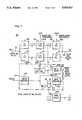
- FIG. 3shows a simplified representation of the computer system of the present invention as including a computer system unit 200 to which a monitor 205, a keyboard input device 210, a mouse input device 215 and a printer output device 220 are coupled.
- FIG. 4is a block diagram of computer system unit 200.
- System unit 200includes a processor 225, for example a 32 bit processor such as the Intel 80386 processor.
- a CPU local bus 230is formed by a 36 bit address bus, a 32 bit data bus and a 10 bit control bus which are coupled between processor 225 and a buffer 240 as shown in FIG. 4.
- a math coprocessor 245such as the Intel 80387 coprocessor is coupled to CPU local bus 230 to perform floating point operations to enhance system throughput.
- System unit 200includes a system local bus 250 coupled between buffer 240 and a buffer 253.
- the system local bus 250includes a data bus, an address bus and a control bus as shown in FIG. 4.
- Buffer 240acts to buffer the address bus of CPU local bus 230 with respect to the address bus of system local bus 250.
- Buffer 240also buffers the data bus and control bus of the CPU local bus 230 with respect to the data bus and control bus of system local bus 250.
- a CPU data cache 255for example a data cache including 64K of memory, is coupled to the address and data busses of CPU local bus 230.
- a cache controller 260such as the Intel 82385 cache controller, for example, is coupled to the address and control busses of CPU local bus 230.
- Cache controller 260controls the storage and access of frequently used data which is stored in data cache 255 to effectively speed up the operation of system unit 200.
- Cache controller 260is also coupled to the address bus of system local bus 250.
- System unit 200includes a bus control and timing circuit 265 coupled to the address, data and control busses of the system local bus 250.
- the system local bus 250is coupled via a latch/buffer/decoder 267 to an input/output (I/O) bus 270 which includes a 10 bit address bus, an 8 bit data bus and a control bus.
- Buffer/decoder 267provides I/O address latch and I/O data buffer steering control.
- Buffer/decoder 267decodes the system local bus address and control signals, and provides "chip select" and I/O command signals to the I/O bus 270. It will be appreciated that "chip select” refers to selecting the particular device coupled to I/O bus 270 at which an operation is to be performed.
- I/O bus 270is coupled to a display adapter 275, a CMOS clock 280, a CMOS RAM 285, an RS232 adapter 290, a printer adapter 295 and, a 4 channel timer 300 for general timekeeping functions.
- I/O bus 270is further coupled to a diskette adapter 305, an interrupt controller 310 and a read only memory (ROM) which contains the system Basic Input Output System (BIOS).
- BIOSBasic Input Output System
- a Micro Channel (TM) bus 320 having address, data and control buses thereinis coupled to system local bus 250 via buffer 253.
- the architecture of the Micro Channel busis described in more detail in the IBM PS/2 Model 80 Technical Reference Manual.
- a central arbitration control point (CACP) 325is coupled to Micro Channel bus 320 and bus control and timing circuit 265 for purposes of managing the Micro Channel multi device bus arbitration mechanism. The connection of such central arbitration control point 325 and bus control and timing circuit 265 actually forms part of the Micro Channel bus 320.
- a plurality of Micro Channel sockets 330are coupled to Micro Channel bus 320 as shown in FIG. 4 for receiving feature cards such as memory cards, video adapters, DASD adapters, SCSI adapters and communications adapter cards.
- One or more hardfile/floppy disk sockets 335are coupled to Micro Channel bus 320 to facilitate connection of a hard disk or floppy disk (not shown) to bus 320.
- a direct memory access (DMA) controller 337is coupled to the address, data and control busses of system local bus 250 for the purpose of permitting peripherals such as hard files, floppy disk drives and any Micro Channel DMA slave devices to have direct access to main memory (described below) to avoid having to directly involve processor 225 in data transfers between such peripherals and main memory.
- DMAdirect memory access
- a memory control circuit 340is coupled to system local bus 250 as shown in FIG. 4. The operation of memory control circuit 340 is fully described and specified in the timing diagram of FIG. 5, described later. However, to enhance understanding of memory control circuit 340, it is noted that memory control circuit 340 actually includes three portions, that is, a RAS/CAS decoder 345, an address decoder/multiplexer 350 and a data buffer 355.
- RAS/CAS decoder 345is coupled at its input to the control bus of system local bus 250.
- RAS/CAS decoder 345takes address and bus cycle definition signals from processor 225 and decodes them to extract memory select and memory timing signals.
- RAS/CAS decoder 345decodes RAS and CAS signals.
- the RAS signal decoded by decoder 345specifies which memory bank, of 8 memory banks, (each bank including 1 megabyte organized as 256K ⁇ 36 bits) is to be accessed during the current memory cycle. The arrangement of these 8 memory banks into a memory 370 including modules 371, 372, 373 and 374 is described later.
- the CAS signal decoded by decoder 345specifies which byte or bytes of a 32 bit word stored in memory 370 are to be accessed during the current memory cycle.
- Memory control circuit 340is coupled to the aforementioned memory 370 in the manner described subsequently.
- Memory 370includes 4 modules of random access memory (RAM), namely modules 371, 372, 373 and 374 each of which accommodates 2 megabytes of memory.
- modules 371-374are designated as dynamic random access memory (DRAM) single inline packages (SIP) or DRAM SIP.
- DRAMdynamic random access memory
- SIPsingle inline packages
- Module 371is populated with 2 Megabytes of memory and is labelled "BASIC 2MB”.
- the remaining modules 372-374are fillable with memory at the user's option and are thus labelled "OPTIONAL 2MB".
- the RAS/CAS decoder 345includes an output bus 380 having 13 separate lines on which the RAS, CAS and WE signals are transmitted to each of memory banks 371-374 of which 8 lines are dedicated to RAS, 4 lines are dedicated to CAS and 1 line is dedicated to WE.
- RAS/CAS decoder 345generates a write enable (WE) signal which designates whether a particular memory cycle is a read cycle or a write cycle and provides that information to memory 370.
- WEwrite enable
- Each of modules 371-374includes 2 megabytes of memory each megabyte of which is divided into 512 pages or rows which are 2K bytes long each. That is, banks 371-374 are configured as page mode memories.
- Address multiplexer (ADDR MUX) 350is coupled at its input to the 36 line data bus of system local bus 250.
- processor 225desires to access a piece of data stored in a location in memory 370
- processor 225transmits the 36 bits of the address of that memory location to address multiplexer 350.
- Address multiplexer 350derives the page address (row address) and column address from the 36 bit address information and provides the page address and column address to memory 370 via a multiplexed address (MUX ADDR) bus 390 which couples address multiplexer 350 to memory 370.
- a 36 bit memory data bus 400couples memory modules 371-374 of memory 370 to data buffer 355.
- the data at the specified memory addressis transferred to a memory data bus 400 which supplies the data to data buffer 355 as shown in FIG. 4.
- a memory data bus 40032 bits (D 0 -D 31 ) are dedicated to data and 4 parity bits (P 0 -P 3 ) are dedicated to parity.
- the addressed datareaches memory data bus 400, the data is buffered by data buffer 355 and is then placed on the data bus of system local bus 250. Subsequently, the data is passed to processor 225 via buffer 240 and CPU local bus 230.
- timing diagram of FIG. 5Bdescribes in detail the operation of memory control circuit 340 and memory 370.
- the prior art timing diagram of FIG. 2has been repeated in the upper portion of FIG. 5 as FIG. 5A.
- processor 225desires to access a piece of data stored at a selected address or location in memory 370. This piece of data is referred to as the first selected piece of data. It also assumed that after accessing the first selected piece of data, processor 225 desires to access a second selected piece of data at another memory location.
- Processor 225outputs the selected address at which the first piece of data is stored to the data bus of CPU local bus 230.
- the selected addressconsists of 32 address bits A 0 -A 31 and 4 byte enable bits (BE 0 -BE 3 ) bits thus forming a 36 bit address in total.
- the 4 byte enable bits BE 0 -BE 3are used to indicate which bytes (from 1 to 4) are to be retrieved from the (4 byte, 32 bit) data stored at a particular address.
- the selected addressis buffered by buffer 240.
- the selected addressis then transferred to the address bus of system local bus 250 and provided to memory control circuit 340 and address multiplexer 350.
- System unit 200is arranged in this embodiment such that 9 bits of that 36 bit selected address correspond to the page address or row address (RAS address) 410 of the data to be accessed. That is, bits A 11 -A 19 correspond to the RAS address.
- Page address 410is timed to begin at the start of the first memory cycle as indicated in FIG. 5B.
- Address multiplexer 350extracts this 9 bit page address 410 from the 36 bit address and provides this 9 bit page address 410 to memory 370 via a 9 line MUX ADDR (multiplexed address) bus 390 which couples address multiplexer 350 to memory 370.
- MUX ADDRmultipleplexed address
- the RAS signal from memory control circuit 340is high which corresponds to an OFF state in the negative logic convention employed in FIG. 5B.
- memory control circuit 340(via RAS/CAS decode circuit 345) drives RAS low or ON at 415 as seen in FIG. 5B. In this manner the page address to be used by memory 370 to access the specified data is provided to memory 370.
- memory control circuit 370via address multiplexer 350, extracts the 9 bit column address 420 of the data from the 36 bit address and provides that 9 bit column address 420 to memory 370 via MUX ADDR bus 390.
- bits A 2 -A 11correspond to such column address or (CAS) address.
- memory control circuit 340(via RAS/CAS decode circuit 345) drives CAS low or ON at 425.
- the column address to be used by memory 370 to access the specified datais provided to memory 370.
- the page address and the column address of the dataare thus multiplexed onto the same 9 line MUX ADDR bus 390.
- the remaining bits A 17 -A 31are employed by the RAS decoder 345 to indicate which one of modules 371-374 contains the first piece of data which is being addressed.
- a CAS prechargeis conducted at 440.
- the data on memory data bus 400becomes invalid at 442 after a predetermined period of time has passed from the commencement of CAS precharge.
- the latching circuits in data buffer 355latch the data before it becomes invalid, that is, before 442 on the memory data bus timing diagram of FIG. 5B. Those periods of time during which the data on memory data bus 400 is invalid are indicated by cross-hatching on FIG. 5B.
- the end of the CAS prechargedefines the end of the first memory cycle.
- Processor 225transmits the address of the second selected piece of data to memory control circuit 340 along the same data path as that over which the first selected piece of data travelled thereto. If memory control circuit 340 determines that the second selected piece of data to be fetched from memory 370 is in the same page as the first selected piece of data, then as seen in the timing diagram of FIG. 5B, during the CAS precharge at 440, the column address supplied to MUX ADDR bus 390 is changed to the column address of that second piece of data at 445. This column address change occurs before the end of the first memory cycle.
- the CAS prechargeis finished and CAS is driven ON thus starting the second memory cycle at 450.
- the column address corresponding to the second selected piece of datais thus provided to memory 370.
- T CASAfter a time delay T CAS , the data corresponding to that column address and the already prescribed page address becomes valid at 455 on memory data bus 400.
- the datais then immediately latched at 460 by the bidirectional latches contained in data buffer 355. After the buffering/latching action of data buffer 355 has occurred, the latched data (now the second selected piece of data) is provided at 465 to the data bus of system local bus 250 for transfer to processor 225.
- buffer 355when the memory data latch control signal (LEAB0-3) is low, buffer 355 operates in a transparent or passthrough mode. When the memory data latch control signal is high, buffer 355 is storing data by latch action.
- FIG. 6is a flowchart which summarizes the process by which memory accesses are conducted in system unit 200.
- a memory accessbegins when processor 225 employs address pipelining to output a current address at which data is to be retrieved as per block 500 in the flowchart.
- the current addressis transferred to memory control circuit 340 by the bus structure in system unit 200 in the manner already described.
- the current addressis decoded by memory control circuit 340 as per block 505. That is, a page address and a column address are extracted from the current address.
- the page addressis then multiplexed onto the MUX address bus 390 as per block 510, this event signifying the start of the current memory cycle as per block 515.
- the RASis then activated or turned on at block 520 such that memory 370 selects the page address which is presently provided thereto on MUX address bus 390.
- the column addressis then multiplexed onto the MUX address bus 390 as per block 525.
- the CASis activated or turned on at block 530 such that memory 370 selects the column address which is presently provided thereto on MUX address bus 390.
- the address of the desired data stored in memory 370is completely specified and memory 370 transfers the data at the specified address to memory data bus 390 as per block 535.
- the datais latched by the bidirectional latches in data buffer 355 as per block 540 to preserve such data momentarily.
- the datais transferred to system local data bus 250 as per block 545.
- a CAS prechargeis then conducted as per block 550 prior to the end of the current memory cycle.
- the next address to be accessedis then decoded as per block 555.
- a testis conducted in decision block 560 to determine if the next address is located in the same page as that in which the prior address (formerly the current address above) was located. If the next address is not in the same page as the prior address, then process flow continues back to block 510 of FIG. 6 at which the next page address is multiplexed onto MUX address bus 390. However, if the next address is located in the same page as the prior address, then process flow continues to block 565 at which the column address of the next address is multiplexed onto MUX address bus 390. Subsequently, the next memory cycle or second memory cycle is started at block 570 once the CAS precharge has ended.
- CASis activated or turned on as per block 575 such that memory 370 selects the column address which is presently provided thereto on MUX address bus 390.
- the address of the desired data stored in memory 370is once again completely specified and memory 370 transfers the data at the specified address to memory data bus 390 as per block 580.
- the datais latched by the bidirectional latches in data buffer 355 as per block 585 to preserve such data momentarily.
- the datais transferred to system local data bus 250 as per block 590.
- a CAS prechargeis then conducted as per block 595 prior to the end of the current memory cycle.
- the next address to be accessedis then decoded as per block 600 after which flow continues back to decision block 560 at which a decision is again made to determine if the next address is in the same page as the last address.
- FIG. 7shows one of four substantially identical modules employed in data buffer 355 as module 610.
- Buffer module 610includes an 8 bit port 615 which is coupled to data lines D 0 through D 7 of the memory data bus 400.
- Buffer module 610includes a data receiver 620 designated A REC which is coupled to port 615 as shown.
- Data receiver 620is a buffer which acts as an interface between the 0 to 5 volt TTL signal environment present on memory data bus 400 and the 0 to approximately 3 volt environment characteristic of the internal workings of buffer module 610.
- Latch 625is a transparent latch. That is, latch 625 is operable in either a transparent mode or a latch mode in response to an appropriate control signal at control input 625A.
- a low inputcauses a low output and a high input causes a high output. That is, when in transparent mode the 8 bit data presented to the input of latch 625 flows through to the output thereof.
- latch 625when latch 625 is instructed to assume the latch mode via the latch control signal at input 625A (LEAB0) then, when presented with a particular 8 bit input signal, the output assumes a stable state and remains in such state or latched until presented with an appropriate control signal at control input 625A.
- An output driver 630is coupled to the output of latch 625 as shown in FIG. 7.
- Driver 630is designated "B DRV" and acts to interface the 0 through 3 volt internal environment of data buffer 610 to the external 0 through 5 volt TTL environment present at the output of driver 630.
- the 8 bit output of driver 630is coupled to a port 635 which is coupled to 8 data lines designated B0-B7 of the data bus of system local bus 250.
- latch 625has latched the data provided thereto, the system can continue processing data and the signals on memory data bus 400 (D 0 -D 7 ) are free to change while latch 625 holds the old data for later pick up by processor 225 via system local bus 250.
- Driver 630includes a memory data bus gate control input 630A which is designated OEAB0. when the OEAB0 signal is on, driver 630 is activated to pass data therethrough. However, when the OEAB0 signal is off, driver 630 is inactivated.
- the output of latch 625is coupled to the input of an 8 bit parity tree 640. If the 8 inputs to parity tree 640 exhibit an even number of ones, then parity tree 640 generates a single bit output which is a 1 (high) to maintain odd parity. However, if the 8 inputs to parity tree 640 exhibit an odd number of ones, then parity tree 640 generates a single bit output which is 0 (low) to maintain odd parity.
- Data buffer 610includes a GEN/CK receiver 645 having an input designated GEN/CK0 as illustrated in FIG. 7.
- GEN/CK receiver 645is an interface which converts 0-5 volt TTL signals at the input thereof to 0-3 volt signals at the output thereof.
- the value of GEN/CK0depends on the particular type of cycle which processor 225 desires to run next. That is, the GEN/CK0 input signal (see FIG. 5B) exhibits a value of 1 (high) when a memory write cycle is to be conducted and exhibits a value of 0 (low) when a memory read cycle is to be conducted. For purposes of this example, it is assumed that the GEN/CK0 signal has a value of 0 indicating that a read cycle is to be conducted from memory.
- the data and corresponding parity informationhave already been stored in memory 370 and now it is desired to access such data.
- a 32 bit wordcomprised of four 8 bit bytes is to be retrieved from memory 370.
- Four parity bitsare assumed to be stored with such 32 bit word, that is, 1 parity bit being associated with each byte of the 32 bit word.
- the data buffer 610 of FIG. 7is capable of handling 1 byte (8 bits) and 1 parity bit of such 32 bit word.
- the remaining 3 bytes and 3 parity bits of such 32 bit wordare processed by 3 other data buffers similar to data buffer 610 and shown in FIG. 8.
- the output of GEN/CK receiver 645is coupled to the control input 650A of parity driver 650.
- the output of parity tree 640is coupled to the input 650B of parity driver 650 and to one input of a two input exclusive or gate 655.
- Parity driver output 650Bis coupled to the parity line P 0 of the parity bus portion of memory data bus 400. It will be recalled that the 36 bit memory data bus 400 includes lines D 0 -D 31 for the stored 32 bit word and 4 parity lines P 0 -P 3 corresponding to each of the 4 parity bits associated with the 4 bytes which constitute the stored 32 bit word.
- parity line P0is coupled via a parity receiver 660 to the remaining input of exclusive OR gate 655.
- the output of GEN/CK receiver 645is coupled to a control input 655A of exclusive OR gate 655.
- the logic state of the signal provided to control input 655Adetermines whether exclusive OR gate 655 is turned on to permit signals to pass therethrough or is turned off so as not to permit signals to pass therethrough to the output of exclusive OR gate 655.
- the output of exclusive OR gate 655is designated E 0 (error) and coupled to an error driver 665.
- the output of error driver 665is coupled to an error terminal 670 which is designated E. Error driver 665 is not a part of buffer 610 and is described later.
- a parity error generator/checker 680is formed by parity tree 640, GEN/CK receiver 645, parity driver 650, parity receiver 660, exclusive OR gate 655 and error driver 665.
- parity generator/checker 680operates in two modes, that is a parity generation mode when data is written to memory and a parity check mode when data is retrieved or accessed from memory 370. Since the present invention involves accessing data stored in memory 370, the parity check mode of parity generator/checker 680 is now discussed. When the GEN/CK0 input of GEN/CK receiver 645 is low (0), generator/checker circuit 680 enters the parity check mode.
- generator/checker circuit 680enters the parity generation mode.
- receiver 645receives a GEN/CK0 signal of 0 from the external (TTL) environment
- receiver 645interfaces that signal to its output which as already mentioned is a 0 through approximately 3 volt output.
- the output of receiver 645is coupled to control input 650A of parity driver 650 such that the logical low or 0 now appearing at control input 650A causes parity driver 650 to be turned off such that the signal at the output of parity tree 640 is not passed to the parity bus line P 0 of the memory data bus 400.
- generator/checker circuit 680 in the check modeis to in effect compare the stored parity bit P0 associated with a particular byte of data (D 0 -D 7 ) with the actual parity P 0 ' exhibited by that same byte after it has been retrieved from memory 370. If the memory access was accomplished successfully, the parity before the access, P0, should be the same as the parity after access, P 0 '.
- byte D 0 -D 7When byte D 0 -D 7 is fetched from memory 370, it is received by receiver 620 and latched by latch 625. (The particular byte fetched on lines D 0 -D 7 is hereinafter referred to as byte 0.) The 8 bits of byte 0 are thus latched at the output of latch 625 such that the computer system is free to proceed forward and change the signal values on the D 0 -D 7 lines of memory data bus 400.
- latch 625latches, byte 0 is provided to the 8 bit parity tree 640 which derives a parity bit P 0 ' for this just accessed byte 0.
- P 0 'is thus the actual parity exhibited by byte 0 after it has been retrieved from memory 370.
- the P 0 ' parity bitis provided to one input of two input exclusive OR gate 655. It will be recalled that the remaining input of exclusive OR gate 655 is coupled via parity receiver 660 to the P 0 parity line of memory data bus 400. In this manner, when byte 0 is retrieved from memory 370, the parity bit P 0 corresponding to such byte 0 is provided to the remaining input of exclusive OR gate 655. If the P 0 parity bit prior to access is the same as the P 0 parity bit after memory access, that is both zeros or both ones, then exclusive OR gate 655 generates a 0 at its output indicating that there has been no error in retrieving the data byte, byte 0, from memory.
- exclusive OR gate 655generates a 1 at its output indicating that an error has occurred in retrieving byte 0 from memory 370.
- the error output bit at the output of exclusive OR gate 655is interfaced via driver 665 with logical NOR function to error output port 670 which is designated E.
- Eerror output port 670
- generator/checker circuit 680when generator/checker circuit 680 is in the check parity mode, the GENCK0 signal appearing at the output of GEN/CK receiver 645 is low or 0 which activates exclusive OR gate 655.
- the GEN/CK0 signalis high which turns off exclusive OR gate 655.
- the computer systemregularly samples the E output 670 at the end of each memory cycle to determine if an error has occurred.
- data buffer/latch 610also operates in the direction opposite that described above. That is, when the computer system performs a write to memory of a particular 32 bit word including byte 0, byte 1, byte 2 and byte 3, byte 0 of this word is transferred from system local bus 250 through buffer 610 to memory data bus 400.
- the systemprovides byte 0 to port 635 designated B0-B7.
- Port 635is coupled via a receiver 675 to an 8 bit latch 680 as shown in FIG. 7.
- Receiver 675 and latch 680are substantially identical to receiver 620 and latch 625, respectively.
- Latch 680includes a memory data latch control input designated LEBA0 which when driven high or to 1 results in the latching of 8 bit data supplied to latch 680.
- the output of latch 680is coupled via a driver 685 to the D 0 -D 7 data lines of memory data bus 400.
- Driver 685is substantially identical to driver 630 already discussed.
- Driver 685includes a memory data bus gate control input OEBA0 (Output Enable B to A) which when presented with a logical 0 or low signal turns on driver 685 to permit the passage of data therethrough.
- OEBA0Output Enable B to A
- the memory data latch control signal LEBA0(Latch Enable B to A) then instructs latch 680 to latch the data at the output of latch 680 thus permitting the computer system to continue forward and change the signal values on data lines B0-B7 at port 635 of system local data bus 250.
- the OEBA0 memory data bus gate control signal provided to driver 685goes low to turn on driver 685 thus permitting the 8 bits of byte 0 latched at the output of latch 680 to pass through to data lines D 0 -D 7 of memory data bus 400.
- the OEBA0-3 signalsmirror the write enable (WE) signal which memory controller 340 supplies to memory 370.
- the WE signalis high for read cycles and low for write cycles.
- data buffer 355which is dedicated to the handling of 1 byte, B0, of a 4 byte (32 bit) word stored and retrieved from memory 370.
- data latch/buffer 610is replicated four times as seen in FIG. 9.
- these 4 data buffers 610are referred to as data buffer 610-0, 610-1, 610-2 and 610-3 to readily indicate that they handle the byte 0, byte 1, byte 2 and byte 3 portions of the aforementioned 32 bit word to be retrieved from or written to memory 370.
- FIG. 8shows a simplified block diagram of data buffer 355 as including four substantially identical data buffers/latches 610, namely, data buffers 610-0, 610-1, 610-2 and 610-3 for processing bytes 0, byte 1, byte 2 and byte 3, respectively, of a 32 bit word.
- Data buffer 355is described in more detail in the above cross referenced copending patent application entitled Bidirectional Buffer with Latch and Parity Capability Gaudenzi et al U.S. patent application Ser. No. 07/198,981 filed May 26, 1988.
- receiver 620 and driver 685latches 625 and 680, and driver 630 and receiver 675 have been paired together in respective boxes in FIG. 8.
- data buffer 355is situated between the data bus of system local bus 250 and memory data bus 400. More specifically, the D 0 -D 31 data lines of buffer 355 are coupled to the D 0 -D 31 data lines of memory data bus 400. The B0-B31 data lines of buffer 355 are coupled to the B0-B31 data lines of the data bus of system local bus 250.
- Data buffer 355includes 4 parity bit input/outputs P0, P1, P2 and P3 corresponding to the generated or accessed parity of byte 0, byte 1, byte 2 and byte 3, respectively.
- the P0, P1, P2 and P3 parity lines of data buffer 355are coupled to the P0, P1, P2 and P3 parity lines of the 36 line memory data bus 400. It will be recalled that memory data bus 400 includes data lines D 0 -D 31 and parity lines P0-P3.
- the respective parity trees 640 of data buffers 610 0-3determine the parity associated with each of the four bytes, byte 0-byte 3 of the 32 bit data word and supply the four determined parity bits to parity lines P0-P3 for storage in memory 370.
- the 4 parity bits P0-P3 associated with such data wordare retrieved and supplied to the P0-P3 parity lines of data buffer 355.
- the GEN/CK0 GEN/CK1, GEN/CK2 and GEN/CK3 lines of data buffer 355are coupled to corresponding GENCK0-GENCK3 control lines (not shown) included in memory control circuit 340.
- Memory control circuit 340generates a GEN/CK signal such as the GEN/CK0 signal shown in FIG. 5B and supplies the same to the GENCK0-GENCK3 inputs of buffer 355 to instruct 355 as to whether a read or write operation is being conducted. If a write operation is being conducted, then appropriate GENCK0-GENCK3 signals are produced to instruct the respective buffer 610-1 through 610-3 to generate respective parity bits corresponding to the 4 bytes of the 32 bit word being written to memory 370.
- parity trees 640determine the parity P 0 '-P 3 ' of the 4 bytes after retrieval, respectively. If any of the P 0 -P 3 old parity bits failed to match the corresponding P 0 '-P 3 ' new parity bits, then an error signal is produced on the corresponding error line E0-E3 depicted in FIG. 9 at the inputs of error driver 665.
- Error driver 665performs a NOR logic function. If any of error lines E0, E1, E2 and E3 receive an error signal, then the output of error driver 665 also generates such error signal. It is noted that error driver 665 interfaces the low voltage swing environment internal to buffer 355 with the external TTL environment presented to error terminal 670 designated E.
- FIG. 9is a representation of the pin-out of data buffer 355 showing the various inputs and outputs of buffer 355 already discussed above.
- Table 1is included herein to summarize the different states in which data buffer 355 is capable of operating.
- Table 2is included herein to summarize the different states which buffer 355 assumes in response to different GEN/CK signals.
- the OEAB0-3 and GEN/CK0-3 pins on data buffer 355are coupled together and thus the OEAB (memory data bus gate control) signals mirror or track the GEN/CK signals as seen in FIG. 5B.
- a method for accessing memory in such computer systemis also described and is summarized below.
- This methodis used in a computer system including a page mode memory having an address bus and a data bus coupled thereto and further having first, second and subsequent memory cycles associated therewith. More specifically a method for reading information stored in said memory is provide which includes the steps of providing to the memory an address signal corresponding to the location of data to be accessed in the memory.
- the methodincludes the steps of supplying the memory with a row address strobe (RAS) signal during the first memory cycle and applying a column address strobe (CAS) signal to the memory during the first memory cycle and subsequent to the RAS signal.
- the methodincludes latching the memory thus addressed for later transfer on the data bus and performing a CAS precharge on the memory subsequent to the latching step and prior to the end of a first memory cycle.
- RASrow address strobe
- CAScolumn address strobe
Landscapes
- Engineering & Computer Science (AREA)
- Theoretical Computer Science (AREA)
- General Engineering & Computer Science (AREA)
- Physics & Mathematics (AREA)
- General Physics & Mathematics (AREA)
- Software Systems (AREA)
- Computer Security & Cryptography (AREA)
- Dram (AREA)
- Memory System Of A Hierarchy Structure (AREA)
- Techniques For Improving Reliability Of Storages (AREA)
- Debugging And Monitoring (AREA)
- Bus Control (AREA)
- Hardware Redundancy (AREA)
- Memory System (AREA)
- Radar Systems Or Details Thereof (AREA)
Abstract
Description
TABLE 1 ______________________________________ 0-3 OEBA LEBA LEBA 0-3 0-3 0-3 0-3 A-B B-A ______________________________________ .0. X .0. X 1X 1 Transparent Mode .0. X 1 X 2X 2 Data Latched 1 X .0. X 3X 3 Output Dis- abled 1 X 1 X 4X 4 Output Dis- abled/ Data Latched X .0. X .0. X 1 X .0. X 1 X 2 X 1 X .0. X 3 X 1 X 1X 4 ______________________________________
TABLE 2 ______________________________________ GEN/CKx Px ______________________________________ .0. Check Mode Px Input is Compared to Internally Generated Parity Bit for the 8 Corresponding "A" Inputs. Mismatch Drives Error Line Low. 1 Generate Mode-Parity Bit is Driven Out of Output as Follows: 1 If Even Number of 1's on Corresponding "A" Inputs .0. If Odd Number of 1's. ______________________________________ Note: Error Output = "1" if GEN/CK .0.-3 = 1.
Claims (5)
Priority Applications (26)
| Application Number | Priority Date | Filing Date | Title |
|---|---|---|---|
| US07/196,721US5034917A (en) | 1988-05-26 | 1988-05-26 | Computer system including a page mode memory with decreased access time and method of operation thereof |
| AT89302136TATE125058T1 (en) | 1988-05-26 | 1989-03-03 | METHOD AND ARRANGEMENT FOR ADDRESSING A PAGE MODE MEMORY IN A COMPUTER SYSTEM. |
| GB8904917AGB2219418A (en) | 1988-05-26 | 1989-03-03 | Accessing a page mode memory in a computer system |
| EP89302136AEP0343769B1 (en) | 1988-05-26 | 1989-03-03 | Apparatus and method for accessing a page mode memory in a computer system |
| ES89302136TES2075045T3 (en) | 1988-05-26 | 1989-03-03 | DEVICE AND METHOD FOR ACCESSING A MEMORY IN PAGE MODE IN A COMPUTER SYSTEM. |
| DE68923403TDE68923403T2 (en) | 1988-05-26 | 1989-03-03 | Method and arrangement for addressing a page mode memory in a computer system. |
| DE3909896ADE3909896A1 (en) | 1988-05-26 | 1989-03-25 | DEVICE AND METHOD FOR ACCESSING DATA STORED IN A PAGE STORAGE |
| NZ228610ANZ228610A (en) | 1988-05-26 | 1989-04-04 | Page mode memory addressing |
| PH38469APH30402A (en) | 1988-05-26 | 1989-04-10 | Computer system including a page mode memory with decreased access time and method of operation threeof |
| SE8901304ASE8901304L (en) | 1988-05-26 | 1989-04-11 | DEVICE AND PROCEDURE FOR ACCESSING A PAGE MODULE IN A COMPUTER SYSTEM |
| FI891784AFI95971C (en) | 1988-05-26 | 1989-04-14 | Device and method for accessing side-by-side memory in a computer system |
| JP1096568AJPH06101225B2 (en) | 1988-05-26 | 1989-04-18 | Computer system, memory reading method and transfer method in computer system, memory control method and memory controller |
| NO89891581ANO891581L (en) | 1988-05-26 | 1989-04-18 | PROCEDURE AND DEVICE FOR ACCESSING PAGE MODE MEMORY IN A COMPUTER SYSTEM. |
| DK189589ADK189589A (en) | 1988-05-26 | 1989-04-19 | PROCEDURE AND APPARATUS FOR PROVIDING ACCESS TO A SIDE DIVIDED STORAGE IN A COMPUTER |
| BE8900436ABE1003816A4 (en) | 1988-05-26 | 1989-04-20 | APPARATUS AND METHOD FOR ACCESSING DATA IN PAGES stored MEMORY. |
| CN89102626ACN1010809B (en) | 1988-05-26 | 1989-04-25 | Apparatus and method for accessing data stored in a page mode memory |
| KR1019890005467AKR920010950B1 (en) | 1988-05-26 | 1989-04-26 | Computer system and information reading and data transmission method |
| MYPI89000549AMY104737A (en) | 1988-05-26 | 1989-04-26 | Apparatus and method for accessing data stored in a page mode memory. |
| CA000598606ACA1319201C (en) | 1988-05-26 | 1989-05-03 | Apparatus and method for accessing data stored in a page mode memory |
| NL8901237ANL8901237A (en) | 1988-05-26 | 1989-05-18 | EQUIPMENT AND METHOD FOR APPROACHING A MEMORY FOR PAGE PROCESSING METHOD IN A COMPUTER SYSTEM. |
| IN44DE1989DIN175457B (en) | 1988-05-26 | 1989-05-19 | |
| MX016141AMX167244B (en) | 1988-05-26 | 1989-05-22 | DEVICE AND METHOD FOR GIVING ACCESS TO DATA STORED IN A PAGE MODE MEMORY |
| PT90631APT90631B (en) | 1988-05-26 | 1989-05-23 | Apparatus and method for accessing data stored in a report organized in pages |
| IT8920624AIT1230189B (en) | 1988-05-26 | 1989-05-24 | APPARATUS AND METHOD FOR ACCESSING DATA STORED IN A PAGE MODE MEMORY. |
| BR898902399ABR8902399A (en) | 1988-05-26 | 1989-05-24 | COMPUTER SYSTEM, DATA TRANSFER PROCESS AND MEMORY SYSTEM |
| HK23896AHK23896A (en) | 1988-05-26 | 1996-02-08 | Apparatus and method for accessing a page mode memory in a computer system |
Applications Claiming Priority (1)
| Application Number | Priority Date | Filing Date | Title |
|---|---|---|---|
| US07/196,721US5034917A (en) | 1988-05-26 | 1988-05-26 | Computer system including a page mode memory with decreased access time and method of operation thereof |
Publications (1)
| Publication Number | Publication Date |
|---|---|
| US5034917Atrue US5034917A (en) | 1991-07-23 |
Family
ID=22726583
Family Applications (1)
| Application Number | Title | Priority Date | Filing Date |
|---|---|---|---|
| US07/196,721Expired - Fee RelatedUS5034917A (en) | 1988-05-26 | 1988-05-26 | Computer system including a page mode memory with decreased access time and method of operation thereof |
Country Status (24)
| Country | Link |
|---|---|
| US (1) | US5034917A (en) |
| EP (1) | EP0343769B1 (en) |
| JP (1) | JPH06101225B2 (en) |
| KR (1) | KR920010950B1 (en) |
| CN (1) | CN1010809B (en) |
| AT (1) | ATE125058T1 (en) |
| BE (1) | BE1003816A4 (en) |
| BR (1) | BR8902399A (en) |
| CA (1) | CA1319201C (en) |
| DE (2) | DE68923403T2 (en) |
| DK (1) | DK189589A (en) |
| ES (1) | ES2075045T3 (en) |
| FI (1) | FI95971C (en) |
| GB (1) | GB2219418A (en) |
| HK (1) | HK23896A (en) |
| IT (1) | IT1230189B (en) |
| MX (1) | MX167244B (en) |
| MY (1) | MY104737A (en) |
| NL (1) | NL8901237A (en) |
| NO (1) | NO891581L (en) |
| NZ (1) | NZ228610A (en) |
| PH (1) | PH30402A (en) |
| PT (1) | PT90631B (en) |
| SE (1) | SE8901304L (en) |
Cited By (52)
| Publication number | Priority date | Publication date | Assignee | Title |
|---|---|---|---|---|
| US5159679A (en)* | 1988-09-09 | 1992-10-27 | Compaq Computer Corporation | Computer system with high speed data transfer capabilities |
| US5247636A (en)* | 1990-05-31 | 1993-09-21 | International Business Machines Corporation | Digital processor clock circuit |
| US5253214A (en)* | 1991-09-27 | 1993-10-12 | Eastman Kodak Company | High-performance memory controller with application-programmable optimization |
| US5265236A (en)* | 1990-11-29 | 1993-11-23 | Sun Microsystems, Inc. | Method and apparatus for increasing the speed of memory access in a virtual memory system having fast page mode |
| WO1993024885A1 (en)* | 1992-06-04 | 1993-12-09 | Cabletron Systems, Inc. | Adaptive memory controller |
| US5274786A (en)* | 1990-11-28 | 1993-12-28 | Hewlett-Packard Company | Microprocessor memory bus interface for inhibiting relatching of row address portions upon subsequent accesses including a same row address portion |
| US5276856A (en)* | 1989-09-28 | 1994-01-04 | Pixel Semiconductor, Inc. | Memory controller flexible timing control system and method |
| US5278967A (en)* | 1990-08-31 | 1994-01-11 | International Business Machines Corporation | System for providing gapless data transfer from page-mode dynamic random access memories |
| US5283880A (en)* | 1991-01-02 | 1994-02-01 | Compaq Computer Corp. | Method of fast buffer copying by utilizing a cache memory to accept a page of source buffer contents and then supplying these contents to a target buffer without causing unnecessary wait states |
| US5295247A (en)* | 1992-04-17 | 1994-03-15 | Micronics Computers, Inc. | Local IDE (integrated drive electronics) bus architecture |
| US5301299A (en)* | 1990-06-07 | 1994-04-05 | Intel Corporation | Optimized write protocol for memory accesses utilizing row and column strobes |
| US5303364A (en)* | 1989-09-29 | 1994-04-12 | Compaq Computer Corp. | Paged memory controller |
| US5353417A (en)* | 1991-05-28 | 1994-10-04 | International Business Machines Corp. | Personal computer with bus interface controller coupled directly with local processor and input/output data buses and for anticipating memory control changes on arbitration for bus access |
| US5404480A (en)* | 1991-04-04 | 1995-04-04 | Nec Corporation | Information processor comprising a write buffer circuit containing an address buffer and a data buffer corresponding to each other |
| US5450559A (en)* | 1989-05-31 | 1995-09-12 | International Business Machines Corporation | Microcomputer system employing address offset mechanism to increase the supported cache memory capacity |
| US5493666A (en)* | 1990-03-19 | 1996-02-20 | Apple Computer, Inc. | Memory architecture using page mode writes and single level write buffering |
| US5522064A (en)* | 1990-10-01 | 1996-05-28 | International Business Machines Corporation | Data processing apparatus for dynamically setting timings in a dynamic memory system |
| US5551054A (en)* | 1991-11-19 | 1996-08-27 | Adaptec, Inc. | Page mode buffer controller for transferring Nb byte pages between a host and buffer memory without interruption except for refresh |
| WO1996030838A1 (en)* | 1995-03-31 | 1996-10-03 | Samsung & Electronic, Co. Ltd. | Memory controller which executes read and write commands out of order |
| US5638534A (en)* | 1995-03-31 | 1997-06-10 | Samsung Electronics Co., Ltd. | Memory controller which executes read and write commands out of order |
| US5640527A (en)* | 1993-07-14 | 1997-06-17 | Dell Usa, L.P. | Apparatus and method for address pipelining of dynamic random access memory utilizing transparent page address latches to reduce wait states |
| US5644747A (en)* | 1994-03-08 | 1997-07-01 | Nec Corporation | Page mode access memory controller including plural address latches and a comparator |
| US5666494A (en)* | 1995-03-31 | 1997-09-09 | Samsung Electronics Co., Ltd. | Queue management mechanism which allows entries to be processed in any order |
| US5701143A (en)* | 1995-01-31 | 1997-12-23 | Cirrus Logic, Inc. | Circuits, systems and methods for improving row select speed in a row select memory device |
| US5732236A (en)* | 1993-05-28 | 1998-03-24 | Texas Instruments Incorporated | Circuit and method for controlling access to paged DRAM banks with request prioritization and improved precharge schedule |
| US5742849A (en)* | 1993-10-28 | 1998-04-21 | Kabushiki Kaisha Toshiba | High-performance computer system of a parallel write-buffering type |
| US5758107A (en)* | 1994-02-14 | 1998-05-26 | Motorola Inc. | System for offloading external bus by coupling peripheral device to data processor through interface logic that emulate the characteristics of the external bus |
| US5765203A (en)* | 1995-12-19 | 1998-06-09 | Seagate Technology, Inc. | Storage and addressing method for a buffer memory control system for accessing user and error imformation |
| US5778446A (en)* | 1995-03-22 | 1998-07-07 | Ast Research, Inc. | Rule-based optimizing DRAM controller |
| US5778413A (en)* | 1994-10-14 | 1998-07-07 | Compaq Computer Corporation | Programmable memory controller having two level look-up for memory timing parameter |
| US5835945A (en)* | 1990-08-06 | 1998-11-10 | Ncr Corporation | Memory system with write buffer, prefetch and internal caches |
| US5841715A (en)* | 1990-04-18 | 1998-11-24 | Rambus, Inc. | Integrated circuit I/O using high performance bus interface |
| US6052756A (en)* | 1998-01-23 | 2000-04-18 | Oki Electric Industry Co., Ltd. | Memory page management |
| US6209071B1 (en) | 1996-05-07 | 2001-03-27 | Rambus Inc. | Asynchronous request/synchronous data dynamic random access memory |
| US6493775B2 (en)* | 1998-03-19 | 2002-12-10 | Fujitsu Limited | Control for timed access of devices to a system bus |
| US6502161B1 (en) | 2000-01-05 | 2002-12-31 | Rambus Inc. | Memory system including a point-to-point linked memory subsystem |
| US6684285B2 (en) | 1990-04-18 | 2004-01-27 | Rambus Inc. | Synchronous integrated circuit device |
| US20040128460A1 (en)* | 1999-12-09 | 2004-07-01 | Rambus Inc. | Transceiver with latency alignment circuitry |
| US20040186956A1 (en)* | 2000-01-05 | 2004-09-23 | Richard Perego | Configurable width buffered module |
| US20040256638A1 (en)* | 2000-01-05 | 2004-12-23 | Richard Perego | Configurable width buffered module having a bypass circuit |
| US20050007805A1 (en)* | 2000-01-05 | 2005-01-13 | Fred Ware | Configurable width buffered module having flyby elements |
| US20050010737A1 (en)* | 2000-01-05 | 2005-01-13 | Fred Ware | Configurable width buffered module having splitter elements |
| US20050041504A1 (en)* | 2000-01-05 | 2005-02-24 | Perego Richard E. | Method of operating a memory system including an integrated circuit buffer device |
| US20050166026A1 (en)* | 2000-01-05 | 2005-07-28 | Fred Ware | Configurable width buffered module having switch elements |
| US20070002668A1 (en)* | 2005-06-30 | 2007-01-04 | Williams Peter M | Micro-tile memory interfaces |
| US20070013704A1 (en)* | 2005-06-30 | 2007-01-18 | Macwilliams Peter | Memory controller interface for micro-tiled memory access |
| US20070088995A1 (en)* | 2005-09-26 | 2007-04-19 | Rambus Inc. | System including a buffered memory module |
| US20080080261A1 (en)* | 2005-09-26 | 2008-04-03 | Rambus Inc. | Memory system topologies including a buffer device and an integrated circuit memory device |
| US20080162802A1 (en)* | 2006-12-28 | 2008-07-03 | James Akiyama | Accessing memory using multi-tiling |
| US8248884B2 (en) | 1997-10-10 | 2012-08-21 | Rambus Inc. | Method of controlling a memory device having multiple power modes |
| US8607328B1 (en) | 2005-03-04 | 2013-12-10 | David Hodges | Methods and systems for automated system support |
| US11328764B2 (en) | 2005-09-26 | 2022-05-10 | Rambus Inc. | Memory system topologies including a memory die stack |
Families Citing this family (8)
| Publication number | Priority date | Publication date | Assignee | Title |
|---|---|---|---|---|
| DE69323715T2 (en)* | 1993-01-21 | 1999-10-21 | Advanced Micro Devices, Inc. | Electronic storage system and method |
| KR970001699B1 (en)* | 1994-03-03 | 1997-02-13 | 삼성전자 주식회사 | Syncronous semiconductor memory device having the function of automatic precharge |
| JPH08314795A (en)* | 1994-05-19 | 1996-11-29 | Hitachi Ltd | Storage device read circuit and storage system |
| USRE36532E (en)* | 1995-03-02 | 2000-01-25 | Samsung Electronics Co., Ltd. | Synchronous semiconductor memory device having an auto-precharge function |
| US6829184B2 (en)* | 2002-01-28 | 2004-12-07 | Intel Corporation | Apparatus and method for encoding auto-precharge |
| US7315928B2 (en)* | 2005-02-03 | 2008-01-01 | Mediatek Incorporation | Apparatus and related method for accessing page mode flash memory |
| US9773533B2 (en) | 2013-06-06 | 2017-09-26 | Etron Technology, Inc. | Memory with low current consumption and method for reducing current consumption of a memory |
| CN113361683B (en)* | 2021-05-18 | 2023-01-10 | 山东师范大学 | A biomimetic brain storage method and system |
Citations (14)
| Publication number | Priority date | Publication date | Assignee | Title |
|---|---|---|---|---|
| US4239993A (en)* | 1978-09-22 | 1980-12-16 | Texas Instruments Incorporated | High performance dynamic sense amplifier with active loads |
| US4318014A (en)* | 1979-07-27 | 1982-03-02 | Motorola, Inc. | Selective precharge circuit for read-only-memory |
| US4422160A (en)* | 1981-01-08 | 1983-12-20 | Nippon Electric Co., Ltd. | Memory device |
| US4429375A (en)* | 1980-07-23 | 1984-01-31 | Nippon Electric Co., Ltd. | Consecutive addressing of a semiconductor memory |
| EP0145320A2 (en)* | 1983-11-15 | 1985-06-19 | Motorola, Inc. | Method for multiplexing a memory data bus |
| US4581721A (en)* | 1981-11-18 | 1986-04-08 | Texas Instruments Incorporated | Memory apparatus with random and sequential addressing |
| US4623986A (en)* | 1984-02-23 | 1986-11-18 | Texas Instruments Incorporated | Memory access controller having cycle number register for storing the number of column address cycles in a multiple column address/single row address memory access cycle |
| US4625300A (en)* | 1982-12-01 | 1986-11-25 | Texas Instruments Incorporated | Single-ended sense amplifier for dynamic memory array |
| US4649522A (en)* | 1985-02-11 | 1987-03-10 | At&T Bell Laboratories | Fast column access memory |
| US4658381A (en)* | 1985-08-05 | 1987-04-14 | Motorola, Inc. | Bit line precharge on a column address change |
| US4722074A (en)* | 1984-10-31 | 1988-01-26 | Mitsubishi Denki Kabushiki Kaisha | Semiconductor storage unit with I/O bus precharging and equalization |
| US4727517A (en)* | 1984-10-11 | 1988-02-23 | Hitachi, Ltd. | Semiconductor memory with column line voltage sitting circuit |
| US4754433A (en)* | 1986-09-16 | 1988-06-28 | Ibm Corporation | Dynamic ram having multiplexed twin I/O line pairs |
| US4764901A (en)* | 1984-08-03 | 1988-08-16 | Kabushiki Kaisha Toshiba | Semiconductor memory device capable of being accessed before completion of data output |
Family Cites Families (4)
| Publication number | Priority date | Publication date | Assignee | Title |
|---|---|---|---|---|
| FR2541796B1 (en)* | 1983-02-25 | 1987-08-21 | Texas Instruments France | DEVICE FOR DISTRIBUTING THE ACCESS TIME OF A MEMORY ON MULTIPLE USERS |
| JPS6142793A (en)* | 1984-08-02 | 1986-03-01 | Seiko Instr & Electronics Ltd | High speed memory system |
| JPH0799616B2 (en)* | 1984-08-30 | 1995-10-25 | 三菱電機株式会社 | Semiconductor memory device |
| JPS6228994A (en)* | 1985-07-29 | 1987-02-06 | Nec Corp | Memory integrated circuit |
- 1988
- 1988-05-26USUS07/196,721patent/US5034917A/ennot_activeExpired - Fee Related
- 1989
- 1989-03-03EPEP89302136Apatent/EP0343769B1/ennot_activeExpired - Lifetime
- 1989-03-03DEDE68923403Tpatent/DE68923403T2/ennot_activeExpired - Lifetime
- 1989-03-03ESES89302136Tpatent/ES2075045T3/ennot_activeExpired - Lifetime
- 1989-03-03ATAT89302136Tpatent/ATE125058T1/ennot_activeIP Right Cessation
- 1989-03-03GBGB8904917Apatent/GB2219418A/ennot_activeWithdrawn
- 1989-03-25DEDE3909896Apatent/DE3909896A1/enactiveGranted
- 1989-04-04NZNZ228610Apatent/NZ228610A/enunknown
- 1989-04-10PHPH38469Apatent/PH30402A/enunknown
- 1989-04-11SESE8901304Apatent/SE8901304L/ennot_activeApplication Discontinuation
- 1989-04-14FIFI891784Apatent/FI95971C/ennot_activeIP Right Cessation
- 1989-04-18NONO89891581Apatent/NO891581L/enunknown
- 1989-04-18JPJP1096568Apatent/JPH06101225B2/ennot_activeExpired - Lifetime
- 1989-04-19DKDK189589Apatent/DK189589A/ennot_activeApplication Discontinuation
- 1989-04-20BEBE8900436Apatent/BE1003816A4/ennot_activeIP Right Cessation
- 1989-04-25CNCN89102626Apatent/CN1010809B/ennot_activeExpired
- 1989-04-26KRKR1019890005467Apatent/KR920010950B1/ennot_activeExpired
- 1989-04-26MYMYPI89000549Apatent/MY104737A/enunknown
- 1989-05-03CACA000598606Apatent/CA1319201C/ennot_activeExpired - Fee Related
- 1989-05-18NLNL8901237Apatent/NL8901237A/ennot_activeApplication Discontinuation
- 1989-05-22MXMX016141Apatent/MX167244B/enunknown
- 1989-05-23PTPT90631Apatent/PT90631B/ennot_activeIP Right Cessation
- 1989-05-24BRBR898902399Apatent/BR8902399A/ennot_activeApplication Discontinuation
- 1989-05-24ITIT8920624Apatent/IT1230189B/enactive
- 1996
- 1996-02-08HKHK23896Apatent/HK23896A/ennot_activeIP Right Cessation
Patent Citations (15)
| Publication number | Priority date | Publication date | Assignee | Title |
|---|---|---|---|---|
| US4239993A (en)* | 1978-09-22 | 1980-12-16 | Texas Instruments Incorporated | High performance dynamic sense amplifier with active loads |
| US4318014A (en)* | 1979-07-27 | 1982-03-02 | Motorola, Inc. | Selective precharge circuit for read-only-memory |
| US4429375A (en)* | 1980-07-23 | 1984-01-31 | Nippon Electric Co., Ltd. | Consecutive addressing of a semiconductor memory |
| US4422160A (en)* | 1981-01-08 | 1983-12-20 | Nippon Electric Co., Ltd. | Memory device |
| US4581721B1 (en)* | 1981-11-18 | 1998-06-09 | Texas Instruments Inc | Memory apparatus with random and sequential addressing |
| US4581721A (en)* | 1981-11-18 | 1986-04-08 | Texas Instruments Incorporated | Memory apparatus with random and sequential addressing |
| US4625300A (en)* | 1982-12-01 | 1986-11-25 | Texas Instruments Incorporated | Single-ended sense amplifier for dynamic memory array |
| EP0145320A2 (en)* | 1983-11-15 | 1985-06-19 | Motorola, Inc. | Method for multiplexing a memory data bus |
| US4623986A (en)* | 1984-02-23 | 1986-11-18 | Texas Instruments Incorporated | Memory access controller having cycle number register for storing the number of column address cycles in a multiple column address/single row address memory access cycle |
| US4764901A (en)* | 1984-08-03 | 1988-08-16 | Kabushiki Kaisha Toshiba | Semiconductor memory device capable of being accessed before completion of data output |
| US4727517A (en)* | 1984-10-11 | 1988-02-23 | Hitachi, Ltd. | Semiconductor memory with column line voltage sitting circuit |
| US4722074A (en)* | 1984-10-31 | 1988-01-26 | Mitsubishi Denki Kabushiki Kaisha | Semiconductor storage unit with I/O bus precharging and equalization |
| US4649522A (en)* | 1985-02-11 | 1987-03-10 | At&T Bell Laboratories | Fast column access memory |
| US4658381A (en)* | 1985-08-05 | 1987-04-14 | Motorola, Inc. | Bit line precharge on a column address change |
| US4754433A (en)* | 1986-09-16 | 1988-06-28 | Ibm Corporation | Dynamic ram having multiplexed twin I/O line pairs |
Cited By (137)
| Publication number | Priority date | Publication date | Assignee | Title |
|---|---|---|---|---|
| US5159679A (en)* | 1988-09-09 | 1992-10-27 | Compaq Computer Corporation | Computer system with high speed data transfer capabilities |
| US5450559A (en)* | 1989-05-31 | 1995-09-12 | International Business Machines Corporation | Microcomputer system employing address offset mechanism to increase the supported cache memory capacity |
| US5276856A (en)* | 1989-09-28 | 1994-01-04 | Pixel Semiconductor, Inc. | Memory controller flexible timing control system and method |
| US5303364A (en)* | 1989-09-29 | 1994-04-12 | Compaq Computer Corp. | Paged memory controller |
| US5493666A (en)* | 1990-03-19 | 1996-02-20 | Apple Computer, Inc. | Memory architecture using page mode writes and single level write buffering |
| US6728819B2 (en) | 1990-04-18 | 2004-04-27 | Rambus Inc. | Synchronous memory device |
| US6975558B2 (en) | 1990-04-18 | 2005-12-13 | Rambus Inc. | Integrated circuit device |
| US7110322B2 (en) | 1990-04-18 | 2006-09-19 | Rambus Inc. | Memory module including an integrated circuit device |
| US7209997B2 (en) | 1990-04-18 | 2007-04-24 | Rambus Inc. | Controller device and method for operating same |
| US6266285B1 (en) | 1990-04-18 | 2001-07-24 | Rambus Inc. | Method of operating a memory device having write latency |
| US6807598B2 (en) | 1990-04-18 | 2004-10-19 | Rambus Inc. | Integrated circuit device having double data rate capability |
| US6751696B2 (en) | 1990-04-18 | 2004-06-15 | Rambus Inc. | Memory device having a programmable register |
| US6715020B2 (en) | 1990-04-18 | 2004-03-30 | Rambus Inc. | Synchronous integrated circuit device |
| US6697295B2 (en) | 1990-04-18 | 2004-02-24 | Rambus Inc. | Memory device having a programmable register |
| US6684285B2 (en) | 1990-04-18 | 2004-01-27 | Rambus Inc. | Synchronous integrated circuit device |
| US6584037B2 (en) | 1990-04-18 | 2003-06-24 | Rambus Inc | Memory device which samples data after an amount of time transpires |
| US6570814B2 (en) | 1990-04-18 | 2003-05-27 | Rambus Inc. | Integrated circuit device which outputs data after a latency period transpires |
| US6415339B1 (en) | 1990-04-18 | 2002-07-02 | Rambus Inc. | Memory device having a plurality of programmable internal registers and a delay time register |
| US6378020B2 (en) | 1990-04-18 | 2002-04-23 | Rambus Inc. | System having double data transfer rate and intergrated circuit therefor |
| US6260097B1 (en) | 1990-04-18 | 2001-07-10 | Rambus | Method and apparatus for controlling a synchronous memory device |
| US20050033903A1 (en)* | 1990-04-18 | 2005-02-10 | Rambus Inc. | Integrated circuit device |
| US6314051B1 (en) | 1990-04-18 | 2001-11-06 | Rambus Inc. | Memory device having write latency |
| US6185644B1 (en) | 1990-04-18 | 2001-02-06 | Rambus Inc. | Memory system including a plurality of memory devices and a transceiver device |
| US6067592A (en)* | 1990-04-18 | 2000-05-23 | Rambus Inc. | System having a synchronous memory device |
| US6049846A (en)* | 1990-04-18 | 2000-04-11 | Rambus Inc. | Integrated circuit having memory which synchronously samples information with respect to external clock signals |
| US5841715A (en)* | 1990-04-18 | 1998-11-24 | Rambus, Inc. | Integrated circuit I/O using high performance bus interface |
| US5247636A (en)* | 1990-05-31 | 1993-09-21 | International Business Machines Corporation | Digital processor clock circuit |
| US5301299A (en)* | 1990-06-07 | 1994-04-05 | Intel Corporation | Optimized write protocol for memory accesses utilizing row and column strobes |
| US5835945A (en)* | 1990-08-06 | 1998-11-10 | Ncr Corporation | Memory system with write buffer, prefetch and internal caches |
| US5278967A (en)* | 1990-08-31 | 1994-01-11 | International Business Machines Corporation | System for providing gapless data transfer from page-mode dynamic random access memories |
| US5522064A (en)* | 1990-10-01 | 1996-05-28 | International Business Machines Corporation | Data processing apparatus for dynamically setting timings in a dynamic memory system |
| US5274786A (en)* | 1990-11-28 | 1993-12-28 | Hewlett-Packard Company | Microprocessor memory bus interface for inhibiting relatching of row address portions upon subsequent accesses including a same row address portion |
| US5265236A (en)* | 1990-11-29 | 1993-11-23 | Sun Microsystems, Inc. | Method and apparatus for increasing the speed of memory access in a virtual memory system having fast page mode |
| US5283880A (en)* | 1991-01-02 | 1994-02-01 | Compaq Computer Corp. | Method of fast buffer copying by utilizing a cache memory to accept a page of source buffer contents and then supplying these contents to a target buffer without causing unnecessary wait states |
| US5404480A (en)* | 1991-04-04 | 1995-04-04 | Nec Corporation | Information processor comprising a write buffer circuit containing an address buffer and a data buffer corresponding to each other |
| US5353417A (en)* | 1991-05-28 | 1994-10-04 | International Business Machines Corp. | Personal computer with bus interface controller coupled directly with local processor and input/output data buses and for anticipating memory control changes on arbitration for bus access |
| US5253214A (en)* | 1991-09-27 | 1993-10-12 | Eastman Kodak Company | High-performance memory controller with application-programmable optimization |
| US5551054A (en)* | 1991-11-19 | 1996-08-27 | Adaptec, Inc. | Page mode buffer controller for transferring Nb byte pages between a host and buffer memory without interruption except for refresh |
| US5295247A (en)* | 1992-04-17 | 1994-03-15 | Micronics Computers, Inc. | Local IDE (integrated drive electronics) bus architecture |
| WO1993024885A1 (en)* | 1992-06-04 | 1993-12-09 | Cabletron Systems, Inc. | Adaptive memory controller |
| AU660559B2 (en)* | 1992-06-04 | 1995-06-29 | Cabletron Systems, Inc. | Adaptive memory controller |
| US5732236A (en)* | 1993-05-28 | 1998-03-24 | Texas Instruments Incorporated | Circuit and method for controlling access to paged DRAM banks with request prioritization and improved precharge schedule |
| US5640527A (en)* | 1993-07-14 | 1997-06-17 | Dell Usa, L.P. | Apparatus and method for address pipelining of dynamic random access memory utilizing transparent page address latches to reduce wait states |
| US5742849A (en)* | 1993-10-28 | 1998-04-21 | Kabushiki Kaisha Toshiba | High-performance computer system of a parallel write-buffering type |
| US5758107A (en)* | 1994-02-14 | 1998-05-26 | Motorola Inc. | System for offloading external bus by coupling peripheral device to data processor through interface logic that emulate the characteristics of the external bus |
| US5644747A (en)* | 1994-03-08 | 1997-07-01 | Nec Corporation | Page mode access memory controller including plural address latches and a comparator |
| US5778413A (en)* | 1994-10-14 | 1998-07-07 | Compaq Computer Corporation | Programmable memory controller having two level look-up for memory timing parameter |
| US5701143A (en)* | 1995-01-31 | 1997-12-23 | Cirrus Logic, Inc. | Circuits, systems and methods for improving row select speed in a row select memory device |
| US5778446A (en)* | 1995-03-22 | 1998-07-07 | Ast Research, Inc. | Rule-based optimizing DRAM controller |
| US5666494A (en)* | 1995-03-31 | 1997-09-09 | Samsung Electronics Co., Ltd. | Queue management mechanism which allows entries to be processed in any order |
| WO1996030838A1 (en)* | 1995-03-31 | 1996-10-03 | Samsung & Electronic, Co. Ltd. | Memory controller which executes read and write commands out of order |
| US5638534A (en)* | 1995-03-31 | 1997-06-10 | Samsung Electronics Co., Ltd. | Memory controller which executes read and write commands out of order |
| US5765203A (en)* | 1995-12-19 | 1998-06-09 | Seagate Technology, Inc. | Storage and addressing method for a buffer memory control system for accessing user and error imformation |
| US7315929B2 (en) | 1996-05-07 | 2008-01-01 | Rambus Inc. | Memory device |
| US20070201280A1 (en)* | 1996-05-07 | 2007-08-30 | Rambus Inc. | Memory device |
| US6405296B1 (en) | 1996-05-07 | 2002-06-11 | Rambus Inc. | Asynchronous request/synchronous data dynamic random access memory |
| US7085906B2 (en) | 1996-05-07 | 2006-08-01 | Rambus Inc. | Memory device |
| US20030061460A1 (en)* | 1996-05-07 | 2003-03-27 | Barth Richard Maurice | Asynchronous request/synchronous data dynamic random access memory |
| US6542976B2 (en) | 1996-05-07 | 2003-04-01 | Rambus Inc. | Memory device having an internal register |
| US6532522B1 (en) | 1996-05-07 | 2003-03-11 | Rambus Inc. | Asynchronous request/synchronous data dynamic random access memory |
| US6209071B1 (en) | 1996-05-07 | 2001-03-27 | Rambus Inc. | Asynchronous request/synchronous data dynamic random access memory |
| US8305839B2 (en) | 1997-10-10 | 2012-11-06 | Rambus Inc. | Memory device having multiple power modes |
| US8248884B2 (en) | 1997-10-10 | 2012-08-21 | Rambus Inc. | Method of controlling a memory device having multiple power modes |
| US6052756A (en)* | 1998-01-23 | 2000-04-18 | Oki Electric Industry Co., Ltd. | Memory page management |
| US6493775B2 (en)* | 1998-03-19 | 2002-12-10 | Fujitsu Limited | Control for timed access of devices to a system bus |
| US8086812B2 (en) | 1999-12-09 | 2011-12-27 | Rambus Inc. | Transceiver with latency alignment circuitry |
| US20070011426A1 (en)* | 1999-12-09 | 2007-01-11 | Rambus Inc. | Transceiver with latency alignment circuitry |
| US7124270B2 (en) | 1999-12-09 | 2006-10-17 | Rambus Inc. | Transceiver with latency alignment circuitry |
| US20050149685A1 (en)* | 1999-12-09 | 2005-07-07 | Kevin Donnelly | Transceiver with latency alignment circuitry |
| US20050160247A1 (en)* | 1999-12-09 | 2005-07-21 | Dillon John B. | Transceiver with latency alignment circuitry |
| US20040128460A1 (en)* | 1999-12-09 | 2004-07-01 | Rambus Inc. | Transceiver with latency alignment circuitry |
| US7065622B2 (en) | 1999-12-09 | 2006-06-20 | Rambus Inc. | Transceiver with latency alignment circuitry |
| US7010658B2 (en) | 1999-12-09 | 2006-03-07 | Rambus Inc. | Transceiver with latency alignment circuitry |
| US20050156934A1 (en)* | 2000-01-05 | 2005-07-21 | Perego Richard E. | System featuring memory modules that include an integrated circuit buffer devices |
| US7200710B2 (en) | 2000-01-05 | 2007-04-03 | Rambus Inc. | Buffer device and method of operation in a buffer device |
| US7000062B2 (en) | 2000-01-05 | 2006-02-14 | Rambus Inc. | System and method featuring a controller device and a memory module that includes an integrated circuit buffer device and a plurality of integrated circuit memory devices |
| US7003618B2 (en) | 2000-01-05 | 2006-02-21 | Rambus Inc. | System featuring memory modules that include an integrated circuit buffer devices |
| US20050210196A1 (en)* | 2000-01-05 | 2005-09-22 | Perego Richard E | Memory module having an integrated circuit buffer device |
| US7010642B2 (en) | 2000-01-05 | 2006-03-07 | Rambus Inc. | System featuring a controller device and a memory module that includes an integrated circuit buffer device and a plurality of integrated circuit memory devices |
| US7017002B2 (en) | 2000-01-05 | 2006-03-21 | Rambus, Inc. | System featuring a master device, a buffer device and a plurality of integrated circuit memory devices |
| US20060067141A1 (en)* | 2000-01-05 | 2006-03-30 | Perego Richard E | Integrated circuit buffer device |
| US7051151B2 (en) | 2000-01-05 | 2006-05-23 | Rambus Inc. | Integrated circuit buffer device |
| US7062597B2 (en) | 2000-01-05 | 2006-06-13 | Rambus Inc. | Integrated circuit buffer device |
| US20050207255A1 (en)* | 2000-01-05 | 2005-09-22 | Perego Richard E | System having a controller device, a buffer device and a plurality of memory devices |
| US20050193163A1 (en)* | 2000-01-05 | 2005-09-01 | Perego Richard E. | Integrated circuit buffer device |
| US20050166026A1 (en)* | 2000-01-05 | 2005-07-28 | Fred Ware | Configurable width buffered module having switch elements |
| US20050149662A1 (en)* | 2000-01-05 | 2005-07-07 | Perego Richard E. | System having a plurality of integrated circuit buffer devices |
| US7526597B2 (en) | 2000-01-05 | 2009-04-28 | Rambus Inc. | Buffered memory having a control bus and dedicated data lines |
| US20050044303A1 (en)* | 2000-01-05 | 2005-02-24 | Perego Richard E. | Memory system including an integrated circuit buffer device |
| US6502161B1 (en) | 2000-01-05 | 2002-12-31 | Rambus Inc. | Memory system including a point-to-point linked memory subsystem |
| US7523248B2 (en) | 2000-01-05 | 2009-04-21 | Rambus Inc. | System having a controller device, a buffer device and a plurality of memory devices |
| US7206896B2 (en) | 2000-01-05 | 2007-04-17 | Rambus Inc. | Integrated circuit buffer device |
| US7206897B2 (en) | 2000-01-05 | 2007-04-17 | Rambus Inc. | Memory module having an integrated circuit buffer device |
| US20040186956A1 (en)* | 2000-01-05 | 2004-09-23 | Richard Perego | Configurable width buffered module |
| US20050041504A1 (en)* | 2000-01-05 | 2005-02-24 | Perego Richard E. | Method of operating a memory system including an integrated circuit buffer device |
| US20050010737A1 (en)* | 2000-01-05 | 2005-01-13 | Fred Ware | Configurable width buffered module having splitter elements |
| US7266634B2 (en) | 2000-01-05 | 2007-09-04 | Rambus Inc. | Configurable width buffered module having flyby elements |
| US20050007805A1 (en)* | 2000-01-05 | 2005-01-13 | Fred Ware | Configurable width buffered module having flyby elements |
| US7320047B2 (en) | 2000-01-05 | 2008-01-15 | Rambus Inc. | System having a controller device, a buffer device and a plurality of memory devices |
| US20080034130A1 (en)* | 2000-01-05 | 2008-02-07 | Rambus Inc. | Buffered Memory Having A Control Bus And Dedicated Data Lines |
| US20050223179A1 (en)* | 2000-01-05 | 2005-10-06 | Perego Richard E | Buffer device and method of operation in a buffer device |
| US7356639B2 (en) | 2000-01-05 | 2008-04-08 | Rambus Inc. | Configurable width buffered module having a bypass circuit |
| US7363422B2 (en) | 2000-01-05 | 2008-04-22 | Rambus Inc. | Configurable width buffered module |
| US20080109596A1 (en)* | 2000-01-05 | 2008-05-08 | Rambus Inc. | System Having A Controller Device, A Buffer Device And A Plurality Of Memory Devices |
| US20040256638A1 (en)* | 2000-01-05 | 2004-12-23 | Richard Perego | Configurable width buffered module having a bypass circuit |
| US20090319719A1 (en)* | 2000-01-05 | 2009-12-24 | Rambus Inc. | System Having A Controller Device, A Buffer Device And A Plurality Of Memory Devices |
| US7404032B2 (en) | 2000-01-05 | 2008-07-22 | Rambus Inc. | Configurable width buffered module having switch elements |
| US8607328B1 (en) | 2005-03-04 | 2013-12-10 | David Hodges | Methods and systems for automated system support |
| US8200883B2 (en) | 2005-06-30 | 2012-06-12 | Intel Corporation | Micro-tile memory interfaces |
| US20110225390A1 (en)* | 2005-06-30 | 2011-09-15 | Peter Mac Williams | Micro-Tile Memory Interfaces |
| US8866830B2 (en) | 2005-06-30 | 2014-10-21 | Intel Corporation | Memory controller interface for micro-tiled memory access |
| US20070002668A1 (en)* | 2005-06-30 | 2007-01-04 | Williams Peter M | Micro-tile memory interfaces |
| US20070013704A1 (en)* | 2005-06-30 | 2007-01-18 | Macwilliams Peter | Memory controller interface for micro-tiled memory access |
| US8253751B2 (en)* | 2005-06-30 | 2012-08-28 | Intel Corporation | Memory controller interface for micro-tiled memory access |
| US8032688B2 (en)* | 2005-06-30 | 2011-10-04 | Intel Corporation | Micro-tile memory interfaces |
| US8539152B2 (en) | 2005-09-26 | 2013-09-17 | Rambus Inc. | Memory system topologies including a buffer device and an integrated circuit memory device |
| US10535398B2 (en) | 2005-09-26 | 2020-01-14 | Rambus Inc. | Memory system topologies including a buffer device and an integrated circuit memory device |
| US20080144411A1 (en)* | 2005-09-26 | 2008-06-19 | Rambus Inc. | Memory Module Including A Plurality Of Integrated Circuit Memory Devices And A Plurality Of Buffer Devices In A Matrix Topology |
| US8108607B2 (en)* | 2005-09-26 | 2012-01-31 | Rambus Inc. | Memory system topologies including a buffer device and an integrated circuit memory device |
| US20080080261A1 (en)* | 2005-09-26 | 2008-04-03 | Rambus Inc. | Memory system topologies including a buffer device and an integrated circuit memory device |
| US20070088995A1 (en)* | 2005-09-26 | 2007-04-19 | Rambus Inc. | System including a buffered memory module |
| US7685364B2 (en) | 2005-09-26 | 2010-03-23 | Rambus Inc. | Memory system topologies including a buffer device and an integrated circuit memory device |
| US12394471B2 (en) | 2005-09-26 | 2025-08-19 | Rambus Inc. | Memory system topologies including a memory die stack |
| US7464225B2 (en) | 2005-09-26 | 2008-12-09 | Rambus Inc. | Memory module including a plurality of integrated circuit memory devices and a plurality of buffer devices in a matrix topology |
| US20090198924A1 (en)* | 2005-09-26 | 2009-08-06 | Rambus Inc. | Memory System Topologies Including A Buffer Device And An Integrated Circuit Memory Device |
| US7562271B2 (en) | 2005-09-26 | 2009-07-14 | Rambus Inc. | Memory system topologies including a buffer device and an integrated circuit memory device |
| US11727982B2 (en) | 2005-09-26 | 2023-08-15 | Rambus Inc. | Memory system topologies including a memory die stack |
| US9117035B2 (en) | 2005-09-26 | 2015-08-25 | Rambus Inc. | Memory system topologies including a buffer device and an integrated circuit memory device |
| US9563583B2 (en) | 2005-09-26 | 2017-02-07 | Rambus Inc. | Memory system topologies including a buffer device and an integrated circuit memory device |
| US9865329B2 (en) | 2005-09-26 | 2018-01-09 | Rambus Inc. | Memory system topologies including a buffer device and an integrated circuit memory device |
| US10381067B2 (en) | 2005-09-26 | 2019-08-13 | Rambus Inc. | Memory system topologies including a buffer device and an integrated circuit memory device |
| US7729151B2 (en) | 2005-09-26 | 2010-06-01 | Rambus Inc. | System including a buffered memory module |
| US10672458B1 (en) | 2005-09-26 | 2020-06-02 | Rambus Inc. | Memory system topologies including a buffer device and an integrated circuit memory device |
| US11043258B2 (en) | 2005-09-26 | 2021-06-22 | Rambus Inc. | Memory system topologies including a memory die stack |
| US11328764B2 (en) | 2005-09-26 | 2022-05-10 | Rambus Inc. | Memory system topologies including a memory die stack |
| US8878860B2 (en) | 2006-12-28 | 2014-11-04 | Intel Corporation | Accessing memory using multi-tiling |
| US20080162802A1 (en)* | 2006-12-28 | 2008-07-03 | James Akiyama | Accessing memory using multi-tiling |
Also Published As
Similar Documents
| Publication | Publication Date | Title |
|---|---|---|
| US5034917A (en) | Computer system including a page mode memory with decreased access time and method of operation thereof | |
| US5757703A (en) | Distributed write data drivers for burst access memories | |
| US7646654B2 (en) | Distributed write data drivers for burst access memories | |
| US5218686A (en) | Combined synchronous and asynchronous memory controller | |
| US6728142B2 (en) | Distributed write data drivers for burst access memories | |
| US6519689B2 (en) | Method and system for processing pipelined memory commands | |
| JPH04230544A (en) | Data processing apparatus for dynamically setting timing of dynamic memory system | |
| US6931483B2 (en) | Memory device having different burst order addressing for read and write operations | |
| JPH02223091A (en) | Computer memory system | |
| JP2000506301A (en) | Simplified clocked DRAM with fast command input | |
| EP0607668B1 (en) | Electronic memory system and method | |
| AU611275B2 (en) | Apparatus and method for accessing data stored in a page mode memory | |
| JP2007328910A (en) | Main memory system with multiple data paths | |
| JP2002358783A (en) | Data input/output method, and dram | |
| WO1997002571A1 (en) | Distributed write data drivers for burst memories |
Legal Events
| Date | Code | Title | Description |
|---|---|---|---|
| AS | Assignment | Owner name:INTERNATIONAL BUSINESS MACHINES CORPORATION, ARMON Free format text:ASSIGNMENT OF ASSIGNORS INTEREST.;ASSIGNORS:BLAND, PATRICK M.;DEAN, MARK E.;REEL/FRAME:004883/0418 Effective date:19880525 Owner name:INTERNATIONAL BUSINESS MACHINES CORPORATION, A COR Free format text:ASSIGNMENT OF ASSIGNORS INTEREST;ASSIGNORS:BLAND, PATRICK M.;DEAN, MARK E.;REEL/FRAME:004883/0418 Effective date:19880525 | |
| FPAY | Fee payment | Year of fee payment:4 | |
| FPAY | Fee payment | Year of fee payment:8 | |
| REMI | Maintenance fee reminder mailed | ||
| LAPS | Lapse for failure to pay maintenance fees | ||
| STCH | Information on status: patent discontinuation | Free format text:PATENT EXPIRED DUE TO NONPAYMENT OF MAINTENANCE FEES UNDER 37 CFR 1.362 | |
| FP | Lapsed due to failure to pay maintenance fee | Effective date:20030723 | |
| AS | Assignment | Owner name:LENOVO (SINGAPORE) PTE LTD.,SINGAPORE Free format text:ASSIGNMENT OF ASSIGNORS INTEREST;ASSIGNOR:INTERNATIONAL BUSINESS MACHINES CORPORATION;REEL/FRAME:016891/0507 Effective date:20050520 Owner name:LENOVO (SINGAPORE) PTE LTD., SINGAPORE Free format text:ASSIGNMENT OF ASSIGNORS INTEREST;ASSIGNOR:INTERNATIONAL BUSINESS MACHINES CORPORATION;REEL/FRAME:016891/0507 Effective date:20050520 |