US5030961A - Microstrip antenna with bent feed board - Google Patents
Microstrip antenna with bent feed boardDownload PDFInfo
- Publication number
- US5030961A US5030961AUS07/508,217US50821790AUS5030961AUS 5030961 AUS5030961 AUS 5030961AUS 50821790 AUS50821790 AUS 50821790AUS 5030961 AUS5030961 AUS 5030961A
- Authority
- US
- United States
- Prior art keywords
- circuit board
- microstrip antenna
- recited
- feed circuit
- shaped
- Prior art date
- Legal status (The legal status is an assumption and is not a legal conclusion. Google has not performed a legal analysis and makes no representation as to the accuracy of the status listed.)
- Expired - Lifetime
Links
- 238000001816coolingMethods0.000claimsabstractdescription4
- 230000008878couplingEffects0.000claimsdescription3
- 238000010168coupling processMethods0.000claimsdescription3
- 238000005859coupling reactionMethods0.000claimsdescription3
- 206010044334TranceDiseases0.000claims1
- 230000005855radiationEffects0.000claims1
- 230000017525heat dissipationEffects0.000abstractdescription4
- 239000002184metalSubstances0.000abstractdescription3
- 239000000758substrateSubstances0.000description6
- 239000010410layerSubstances0.000description4
- 230000004075alterationEffects0.000description2
- 238000005530etchingMethods0.000description2
- 238000004519manufacturing processMethods0.000description2
- 230000004048modificationEffects0.000description2
- 238000012986modificationMethods0.000description2
- 239000011152fibreglassSubstances0.000description1
- 230000010354integrationEffects0.000description1
- 239000000463materialSubstances0.000description1
- 239000007769metal materialSubstances0.000description1
- 238000007747platingMethods0.000description1
- 239000002356single layerSubstances0.000description1
Images
Classifications
- H—ELECTRICITY
- H01—ELECTRIC ELEMENTS
- H01Q—ANTENNAS, i.e. RADIO AERIALS
- H01Q21/00—Antenna arrays or systems
- H01Q21/06—Arrays of individually energised antenna units similarly polarised and spaced apart
- H01Q21/061—Two dimensional planar arrays
- H01Q21/065—Patch antenna array
- H—ELECTRICITY
- H01—ELECTRIC ELEMENTS
- H01Q—ANTENNAS, i.e. RADIO AERIALS
- H01Q21/00—Antenna arrays or systems
- H01Q21/0006—Particular feeding systems
- H—ELECTRICITY
- H01—ELECTRIC ELEMENTS
- H01Q—ANTENNAS, i.e. RADIO AERIALS
- H01Q21/00—Antenna arrays or systems
- H01Q21/0087—Apparatus or processes specially adapted for manufacturing antenna arrays
Definitions
- the present inventionrelates generally to microstrip antenna apparatus and more particularly to an improved microstrip antenna array structure in which bent or folded circuit boards are used to significantly increase the surface area available for the integration of circuits and components on a single layer of feed circuit board.
- the conventional multiple layer laminated structureconsists of multiple layers of circuit boards with patch radiating elements, RF power combining network, control logic circuit, and active components residing on the various layers.
- the electrical interconnections between boardsis usually accomplished by via-holes.
- the use of multiple layersis necessary because the spacing between the antenna elements, typically on the order of 0.5 to 0.7 wavelengths, is too small to allow sufficient surface area behind each radiating element to accommodate all of the circuitry in one layer. Accordingly, fabrication of such an antenna is usually complex and expensive. Furthermore, it requires a high degree of precision in aligning the various boards which often have different thermal and mechanical properties. Via-hole etching through multiple boards can be used to overcome some of the problems but is very costly and the heat dissipation associated with any active components embedded in the mid-layers is nearly always a problem.
- a presently preferred embodiment of the present inventionincludes an orthogonal planar array (12) of patch radiators with specially configured feed boards (16) provided for each column of array elements.
- Each such boardincludes a portion disposed parallel to the plane of the array (12) and one or more portions bent or folded to extend in the direction of the array axis for a distance sufficient to accommodate necessary circuitry (36) and active devices (40).
- a metal supporting frame (20)serves both as a common ground for the assembly and as a heat sink for conducting some of the heat generated by the active devices mounted to the feed boards.
- An additional planar circuit board (22)is positioned beneath the supporting frame (18) to accommodate the power combining circuit and to interconnect all of the elements. Connection between feed boards (16) and combiner board (22) is accomplished using via-connections or a coaxial cable network.
- the hollows formed by the specially configured feed boardsprovide passageways for cooling air circulation and further enhance heat dissipation within the device.
- An important advantage of the present inventionis that the circuitry and active devices needed for an entire column of elements in a phased array can be accommodated in a single feed board.
- Another advantage of the present inventionis that neither multiple board alignment nor multilayer via-hole etching is required.
- Still another advantage of the present inventionis that it inherently provides better heat dissipation within a complex array circuit.
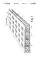
- FIG. 1is a perspective view illustrating a microstrip phased array antenna in accordance with the present invention.
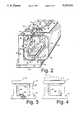
- FIG. 2is a broken away segment of the antenna illustrated in FIG. 1, showing the various components associated with a single patch element.
- FIGS. 3 and 4illustrate alternate configurations for the feed circuit board of the present invention.
- a microstrip phased array antenna devicein accordance with the present invention is depicted which includes a planar array of orthogonally disposed patch radiators 10 formed on the upper surface of an antenna substrate 12 having affixed to the lower surface thereof, a ground plane 14 for the radiators. Lying beneath each column of radiators is a column feed circuit board 16 formed to have a generally C-shaped transverse cross-section. The several feed boards 16 are mounted to a metal supporting frame 18 comprised of a planar base having upstanding ribs 20 extending parallel to the columns and positioned between adjacent boards 16. The frame 18 provides structural rigidity to the device as well as serving as a heat sink. Affixed to the bottom surface of frame 18 is an RF power combiner board which serves to interconnect all of the columns.
- each patch radiator 10is of a suitable metallic material plated to the top surface of a non-conductive substrate 12 which in turn has plated to the bottom side thereof, the ground plane 14.
- Etched from the ground plane 14 during the manufacture thereofis a plurality of rectangular coupling apertures 30, the elongated dimensions of which extend parallel to the column length.
- Each aperture 30is positioned to lie directly beneath the center of a corresponding patch radiator 10.
- Circuit board 16is comprised of a non-conductive substrate 32 having one side continuously plated to provide a ground plane 34 having a plurality of rectangular openings 35 corresponding to the apertures 30, and the other side provided with an array of conductive traces 36 to which the contact pads of an appropriate active device, such as an MIC/MMIC for phase shifters, amplifiers, switches, etc., may be attached.
- a microstrip feed line 38is provided. Feed line 38 extends transverse to the elongated dimension of opening 35 and crosses beneath the center thereof.
- the boardis formed into a channel-like tubular configuration having a generally C-shaped cross-section.
- the vertical sides of feed boards 16can be made of any suitable length to accommodate as many active devices and associated lead traces as is required.
- the column boards 16are positioned within the slots formed by ribs 20, and the pads 42 are via-connected, or alternatively are coaxially connected, to the appropriate traces of the RF combiner board 22.
- the ground plane 34is soldered or otherwise connected to the frame 18.
- the patch array board, including patches 10, substrate 12 and ground plane 14,is then positioned over the assembly with the coupling apertures 30 aligned with the slots 35 in the ground plane 34 of each feed board 16.
- the patch array boardis affixed to the frame and/or feed board assembly by suitable means such as non-conductive clamping screws or pins, or the like (not shown).
- heat generated within the various componentsis conducted to frame 18 and is dissipated thereby.
- convective coolingis provided by the flow of air through the internal passageways formed by the channel-shaped feed boards.
- the non-conductive substrate of feed board 32is comprised of a teflon-impregnated fiberglass material, typically having a thickness of approximately 0.010 to 0.025 inch, and the circuit traces 36 and 38 and ground plane 34 are typically etched metallic platings of thickness within the range 0.0005 to 0.001 inch.
- the thickness of substrate 12is typically two percent (2%) to ten percent (10%) of the operational wavelength of the device.
- a second patch radiator layer(as depicted by the dashed lines 10' in FIG. 4) may be disposed above that depicted.
- the cross-sectional configuration of the feed boards 16may be modified to have other folded configurations which may, for example, be U-shaped, J-shaped, G-shaped or have any other configuration suited to a particular application.
- alternative configurations for the feed boardare suggested.
- One versionis in the form of an L-shaped configuration 50 in which power feed is accomplished through a coaxial connector 52.
- a similar alternative configurationwould be the inverted U-shaped embodiment 54.
- Another variationwould be to foreshorten one of the legs of the U-shaped configuration to provide an inverted J-shaped embodiment.
- Depicted in FIG. 4is an open C-shaped board 56 and an alternate G-shaped board 58, both of which would normally be via-connected to the power combiner.
Landscapes
- Engineering & Computer Science (AREA)
- Manufacturing & Machinery (AREA)
- Waveguide Aerials (AREA)
Abstract
Description
Claims (14)
Priority Applications (1)
| Application Number | Priority Date | Filing Date | Title |
|---|---|---|---|
| US07/508,217US5030961A (en) | 1990-04-10 | 1990-04-10 | Microstrip antenna with bent feed board |
Applications Claiming Priority (1)
| Application Number | Priority Date | Filing Date | Title |
|---|---|---|---|
| US07/508,217US5030961A (en) | 1990-04-10 | 1990-04-10 | Microstrip antenna with bent feed board |
Publications (1)
| Publication Number | Publication Date |
|---|---|
| US5030961Atrue US5030961A (en) | 1991-07-09 |
Family
ID=24021845
Family Applications (1)
| Application Number | Title | Priority Date | Filing Date |
|---|---|---|---|
| US07/508,217Expired - LifetimeUS5030961A (en) | 1990-04-10 | 1990-04-10 | Microstrip antenna with bent feed board |
Country Status (1)
| Country | Link |
|---|---|
| US (1) | US5030961A (en) |
Cited By (18)
| Publication number | Priority date | Publication date | Assignee | Title |
|---|---|---|---|---|
| US5327152A (en)* | 1991-10-25 | 1994-07-05 | Itt Corporation | Support apparatus for an active aperture radar antenna |
| US5448249A (en)* | 1992-02-27 | 1995-09-05 | Murata Manufacturing Co., Ltd. | Antenna device |
| EP0726612A1 (en)* | 1995-02-03 | 1996-08-14 | Gec-Marconi Avionics (Holdings) Limited | Antenna apparatus |
| WO1997043799A1 (en)* | 1996-05-13 | 1997-11-20 | Allgon Ab | Flat antenna |
| US5724048A (en)* | 1991-02-01 | 1998-03-03 | Alcatel, N.V. | Array antenna, in particular for space applications |
| WO1999031757A1 (en)* | 1997-12-12 | 1999-06-24 | Allgon Ab | Dual band antenna |
| US6054953A (en)* | 1998-12-10 | 2000-04-25 | Allgon Ab | Dual band antenna |
| NL1012278C2 (en)* | 1999-06-09 | 2000-12-12 | Libertel Netwerk Bv | Antenna module. |
| US6542122B1 (en)* | 2001-10-16 | 2003-04-01 | Telefonaktiebolaget Lm Ericsson (Publ) | Patch antenna precision connection |
| US6733324B1 (en)* | 2002-12-06 | 2004-05-11 | Com Dev Ltd. | Coaxial heat sink connector |
| US20040130490A1 (en)* | 2001-12-14 | 2004-07-08 | Single Ku-Bank Multi-Polarization Gallium Arsenide Transmit Chip | Single ku-band multi-polarization gallium arsenide transmit chip |
| US20050206575A1 (en)* | 2000-12-21 | 2005-09-22 | Chadwick Peter E | Dual polarisation antenna |
| WO2006086611A2 (en) | 2005-02-11 | 2006-08-17 | Radatec, Inc. | Microstrip patch antenna for high temperature environments |
| US20070152882A1 (en)* | 2006-01-03 | 2007-07-05 | Harris Corporation | Phased array antenna including transverse circuit boards and associated methods |
| US20080106467A1 (en)* | 2006-11-08 | 2008-05-08 | Navarro Julio A | Compact, low profile electronically scanned antenna |
| US20080252547A1 (en)* | 2007-04-12 | 2008-10-16 | General Instrument Corporation | Mechanically Integrated Cable Mesh Antenna System |
| US9225058B2 (en) | 2013-03-15 | 2015-12-29 | Blackberry Limited | Flex PCB folded antenna |
| EP4350756A4 (en)* | 2021-05-26 | 2024-09-11 | Mitsubishi Electric Corporation | Microwave module and antenna apparatus |
Citations (3)
| Publication number | Priority date | Publication date | Assignee | Title |
|---|---|---|---|---|
| US4843400A (en)* | 1988-08-09 | 1989-06-27 | Ford Aerospace Corporation | Aperture coupled circular polarization antenna |
| US4899164A (en)* | 1988-09-16 | 1990-02-06 | The United States Of America As Represented By The Secretary Of The Air Force | Slot coupled microstrip constrained lens |
| US4903033A (en)* | 1988-04-01 | 1990-02-20 | Ford Aerospace Corporation | Planar dual polarization antenna |
- 1990
- 1990-04-10USUS07/508,217patent/US5030961A/ennot_activeExpired - Lifetime
Patent Citations (3)
| Publication number | Priority date | Publication date | Assignee | Title |
|---|---|---|---|---|
| US4903033A (en)* | 1988-04-01 | 1990-02-20 | Ford Aerospace Corporation | Planar dual polarization antenna |
| US4843400A (en)* | 1988-08-09 | 1989-06-27 | Ford Aerospace Corporation | Aperture coupled circular polarization antenna |
| US4899164A (en)* | 1988-09-16 | 1990-02-06 | The United States Of America As Represented By The Secretary Of The Air Force | Slot coupled microstrip constrained lens |
Cited By (28)
| Publication number | Priority date | Publication date | Assignee | Title |
|---|---|---|---|---|
| US5724048A (en)* | 1991-02-01 | 1998-03-03 | Alcatel, N.V. | Array antenna, in particular for space applications |
| US5327152A (en)* | 1991-10-25 | 1994-07-05 | Itt Corporation | Support apparatus for an active aperture radar antenna |
| US5448249A (en)* | 1992-02-27 | 1995-09-05 | Murata Manufacturing Co., Ltd. | Antenna device |
| EP0726612A1 (en)* | 1995-02-03 | 1996-08-14 | Gec-Marconi Avionics (Holdings) Limited | Antenna apparatus |
| US5854607A (en)* | 1995-02-03 | 1998-12-29 | Gec-Marconi Avionics (Holdings) Limited | Arrangement for supplying power to modular elements of a phased array antenna |
| US6008763A (en)* | 1996-05-13 | 1999-12-28 | Allgon Ab | Flat antenna |
| WO1997043799A1 (en)* | 1996-05-13 | 1997-11-20 | Allgon Ab | Flat antenna |
| WO1999031757A1 (en)* | 1997-12-12 | 1999-06-24 | Allgon Ab | Dual band antenna |
| US6054953A (en)* | 1998-12-10 | 2000-04-25 | Allgon Ab | Dual band antenna |
| NL1012278C2 (en)* | 1999-06-09 | 2000-12-12 | Libertel Netwerk Bv | Antenna module. |
| WO2000076024A1 (en)* | 1999-06-09 | 2000-12-14 | Libertel Netwerk B.V. | Antenna module |
| US20050206575A1 (en)* | 2000-12-21 | 2005-09-22 | Chadwick Peter E | Dual polarisation antenna |
| US6542122B1 (en)* | 2001-10-16 | 2003-04-01 | Telefonaktiebolaget Lm Ericsson (Publ) | Patch antenna precision connection |
| US20030071756A1 (en)* | 2001-10-16 | 2003-04-17 | Thomas Bolin | Patch antenna precision connection |
| US20040130490A1 (en)* | 2001-12-14 | 2004-07-08 | Single Ku-Bank Multi-Polarization Gallium Arsenide Transmit Chip | Single ku-band multi-polarization gallium arsenide transmit chip |
| US7009562B2 (en)* | 2001-12-14 | 2006-03-07 | Itt Manufacturing Enterprises, Inc. | Single ku-band multi-polarization gallium arsenide transmit chip |
| US6733324B1 (en)* | 2002-12-06 | 2004-05-11 | Com Dev Ltd. | Coaxial heat sink connector |
| EP1854170A4 (en)* | 2005-02-11 | 2008-11-12 | Radatec Inc | Microstrip patch antenna for high temperature environments |
| WO2006086611A2 (en) | 2005-02-11 | 2006-08-17 | Radatec, Inc. | Microstrip patch antenna for high temperature environments |
| US20070152882A1 (en)* | 2006-01-03 | 2007-07-05 | Harris Corporation | Phased array antenna including transverse circuit boards and associated methods |
| GB2452788B (en)* | 2006-11-08 | 2009-09-30 | Boeing Co | Compact low profile electronically scanned antenna |
| US7417598B2 (en) | 2006-11-08 | 2008-08-26 | The Boeing Company | Compact, low profile electronically scanned antenna |
| GB2452788A (en)* | 2006-11-08 | 2009-03-18 | Boeing Co | Phased antenna array arrangement |
| US20080106467A1 (en)* | 2006-11-08 | 2008-05-08 | Navarro Julio A | Compact, low profile electronically scanned antenna |
| US20080252547A1 (en)* | 2007-04-12 | 2008-10-16 | General Instrument Corporation | Mechanically Integrated Cable Mesh Antenna System |
| US7973721B2 (en)* | 2007-04-12 | 2011-07-05 | General Instrument Corporation | Mechanically integrated cable mesh antenna system |
| US9225058B2 (en) | 2013-03-15 | 2015-12-29 | Blackberry Limited | Flex PCB folded antenna |
| EP4350756A4 (en)* | 2021-05-26 | 2024-09-11 | Mitsubishi Electric Corporation | Microwave module and antenna apparatus |
Similar Documents
| Publication | Publication Date | Title |
|---|---|---|
| US5030961A (en) | Microstrip antenna with bent feed board | |
| US11658390B2 (en) | Wireless communications package with integrated antenna array | |
| US10476148B2 (en) | Antenna integrated printed wiring board (AiPWB) | |
| US9985346B2 (en) | Wireless communications package with integrated antennas and air cavity | |
| US7187342B2 (en) | Antenna apparatus and method | |
| US20200021005A1 (en) | Heat-dissipation mechanism and wireless communication device | |
| US20030112200A1 (en) | Horizontally polarized printed circuit antenna array | |
| EP2071669A2 (en) | Phased array antenna with lattice transformation | |
| US12388191B2 (en) | Millimeter wave antenna array | |
| CN112397889A (en) | chip antenna | |
| KR20230048359A (en) | antenna array | |
| US7289078B2 (en) | Millimeter wave antenna | |
| CN101032053A (en) | Pin fin ground plane for a patch antenna | |
| KR100609204B1 (en) | Electrical components and electrical circuit modules with connected ground planes | |
| US7287987B2 (en) | Electrical connector apparatus and method | |
| TW202213862A (en) | Antenna structure and antenna in package | |
| US12288757B2 (en) | Arrangement comprising an integrated circuit package and a heatsink element | |
| US10321555B1 (en) | Printed circuit board based RF circuit module | |
| US12388189B2 (en) | Orthogonal printed circuit board interface | |
| JPH1131915A (en) | Antennas and array antennas | |
| EP3965303B1 (en) | Wireless communication module | |
| JP7425554B2 (en) | antenna device | |
| TWI765132B (en) | Antenna structure | |
| KR102530829B1 (en) | Chip antenna | |
| US20250233315A1 (en) | Antenna system for wide angle scanning antenna array |
Legal Events
| Date | Code | Title | Description |
|---|---|---|---|
| AS | Assignment | Owner name:FORD AEROSPACE CORPORATION, CALIFORNIA Free format text:ASSIGNMENT OF ASSIGNORS INTEREST.;ASSIGNOR:TSAO, CHICH-HSING A.;REEL/FRAME:005292/0006 Effective date:19900409 | |
| AS | Assignment | Owner name:SPACE SYSTEMS/LORAL, INC., 3825 FABIAN WAY, PALO A Free format text:ASSIGNMENT OF ASSIGNORS INTEREST.;ASSIGNOR:FORD AEROSPACE CORPORATION, A CORP. OF DELAWARE;REEL/FRAME:005635/0274 Effective date:19910215 | |
| STCF | Information on status: patent grant | Free format text:PATENTED CASE | |
| FPAY | Fee payment | Year of fee payment:4 | |
| FEPP | Fee payment procedure | Free format text:PAYOR NUMBER ASSIGNED (ORIGINAL EVENT CODE: ASPN); ENTITY STATUS OF PATENT OWNER: LARGE ENTITY | |
| FPAY | Fee payment | Year of fee payment:8 | |
| AS | Assignment | Owner name:BANK OF AMERICA, N.A. AS COLLATERAL AGENT, NORTH C Free format text:SECURITY INTEREST;ASSIGNOR:SPACE SYSTEMS/LORAL, INC.;REEL/FRAME:013000/0580 Effective date:20011221 | |
| FPAY | Fee payment | Year of fee payment:12 | |
| AS | Assignment | Owner name:SPACE SYSTEMS/LORAL, INC., CALIFORNIA Free format text:RELEASE OF SECURITY INTEREST;ASSIGNOR:BANK OF AMERICA, N.A.;REEL/FRAME:016153/0507 Effective date:20040802 | |
| AS | Assignment | Owner name:JPMORGAN CHASE BANK, N.A., AS ADMINISTRATIVE AGENT Free format text:SECURITY AGREEMENT;ASSIGNOR:SPACE SYSTEMS/LORAL, INC.;REEL/FRAME:021965/0173 Effective date:20081016 | |
| AS | Assignment | Owner name:SPACE SYSTEMS/LORAL, INC., CALIFORNIA Free format text:TERMINATION AND RELEASE OF SECURITY INTEREST IN PATENT RIGHTS;ASSIGNOR:JPMORGAN CHASE BANK, N.A.;REEL/FRAME:029228/0203 Effective date:20121102 |