US5028985A - IC carrier - Google Patents
IC carrierDownload PDFInfo
- Publication number
- US5028985A US5028985AUS07/513,948US51394890AUS5028985AUS 5028985 AUS5028985 AUS 5028985AUS 51394890 AUS51394890 AUS 51394890AUS 5028985 AUS5028985 AUS 5028985A
- Authority
- US
- United States
- Prior art keywords
- package
- carrier frame
- contact
- contact pieces
- carrier
- Prior art date
- Legal status (The legal status is an assumption and is not a legal conclusion. Google has not performed a legal analysis and makes no representation as to the accuracy of the status listed.)
- Expired - Fee Related
Links
Images
Classifications
- H—ELECTRICITY
- H01—ELECTRIC ELEMENTS
- H01L—SEMICONDUCTOR DEVICES NOT COVERED BY CLASS H10
- H01L23/00—Details of semiconductor or other solid state devices
- H—ELECTRICITY
- H05—ELECTRIC TECHNIQUES NOT OTHERWISE PROVIDED FOR
- H05K—PRINTED CIRCUITS; CASINGS OR CONSTRUCTIONAL DETAILS OF ELECTRIC APPARATUS; MANUFACTURE OF ASSEMBLAGES OF ELECTRICAL COMPONENTS
- H05K7/00—Constructional details common to different types of electric apparatus
- H05K7/02—Arrangements of circuit components or wiring on supporting structure
- H05K7/10—Plug-in assemblages of components, e.g. IC sockets
- H05K7/1007—Plug-in assemblages of components, e.g. IC sockets with means for increasing contact pressure at the end of engagement of coupling parts
Definitions
- This inventionrelates to an IC carrier for carrying thereon an IC package so as to facilitate transferring, measuring and the like of the IC package.
- an IC carrier for carrying thereon the IC packageis inverted and mounted on an IC socket.
- a presser cover disposed on the IC socketis closed and locked by a lock member, and the IC carrier together with the contact piece are urged against the contact. Accordingly, it is inconvenient to use in that it is difficult to automate the work of engaging and disengaging a lock lever, and opening and closing an IC presser cover to mount and remove the IC carrier to and from the IC socket. Additionally, heat release of the IC package is not satisfactory because the IC package is covered with the presser cover.
- the present inventionhas been accomplished in order to eliminate the above-mentioned disadvantages.
- Another object of the present inventionis to provide an IC carrier, in which heat release by the IC package is satisfactory.
- a contact insertion space opening up in an inserting direction of a contact of an IC socket, etc.is provided between a frame for forming a supporting seat of an IC contact piece projecting sideways of the IC package and the IC contact insertion space presses the IC contact piece to realize a contact relation.
- the supporting seatmay be provided on an external edge thereof with a tapered portion which gradually slopes downwardly toward the outside of the frame.
- the contact insertion spaceis formed between the tapered portion and the IC contact piece.
- the contactis inserted into and removed from the contact insertion space and the contact is caused to press downwardly against the upper surface of the IC contact piece in order to realize a contacted state.
- the IC packageis held between the contact and the socket, and the IC carrier is held by the socket through the IC package. Therefore, the pressure cover and the lock member as used in the prior art can be omitted.
- the contactcan be displaced forward and backward when it is inserted into and removed from the contact insertion space.
- This kind of displacing operationcan be performed by a robot, etc.
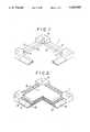
- FIG. 1is a perspective view, partly in section, showing one embodiment of the present invention
- FIG. 2is a perspective view of the above, in which an IC package is already held;
- FIG. 3is a plan view thereof
- FIG. 4is a sectional view thereof
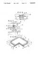
- FIG. 5is a plan view of an IC socket with the IC carrier mounted thereon;
- FIG. 6is a side view thereof
- FIG. 7is a sectional view thereof.
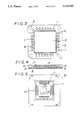
- FIG. 8is a perspective view, partly in section, showing another embodiment in which the IC package is already mounted on the IC carrier.
- FIG. 1is a perspective view, partly in section, showing an IC carrier according to one embodiment of the present invention.
- the numeral 1denotes an IC carrier formed of a generally square-shaped frame 2 which has a square IC package accommodating portion 3 formed in its central portion.
- the IC carrier 1has retaining claws 4 formed on one set of diametrically opposite corners and adapted to hold the IC package, and has U-shaped grooves 5 formed on the other set of diametrically opposite corners and adapted to allow elastic deformation of the IC carrier 1 about a diagonal line.
- Each side of the frame 2 defining the generally square IC package accommodating portion 3has a contact piece supporting seat 8 formed thereon along the upper surface of the frame 2 and adapted to support an IC contact piece 7 of the IC package 6. Furthermore, the contact piece supporting seat 8 has a tapered portion 9 formed on an external edge thereof which gradually lowers toward the outside of the frame.
- the IC package 6is accommodated in the accommodating portion 3 of the IC carrier 1 and is carried by the IC carrier 1 with the retaining claws 4 engaged with the corners of the IC package 6.
- a leading end portion of the IC contact piece 7extends above the tapered portion 9 such that a space is formed between the tapered portion 9 and the leading end, so that a contact 11 of an IC socket 10, etc. can be inserted therein. That is, a contact insertion space 12 opening toward the outside of the frame is formed between the frame forming a contact piece 7. This insertion space 12 is also commonly used for obtaining contact between the contact 11 and the IC contact piece 7.
- FIGS. 5 through 7show one example thereof.
- FIG. 5is a plan view of the IC socket 10 on which the IC package 6 is placed so as to be held on the IC carrier 1
- FIG. 6is a side view thereof
- FIG. 7is a sectional view thereof. Note that FIG. 7 is horizontally symmetric, and that the socket is divided into two halves. However, only one half is shown.
- the IC socket 10has a generally square IC carrier accommodating portion 13 formed in its central portion.
- Four sides of the IC carrier accommodating portion 13are provided with positioning walls 14 for positioning the IC package 6 by restricting the peripheral surface thereof, and four peripheral sides of the IC carrier accommodating portion 13 are provided with elastic contacts for contacting the contact pieces 7 of the IC package 6.
- contact shutter member 15is vertically movably mounted on the IC socket 10 and adapted to move generally backwardly against the elasticity of the contact 11 so as to provide a pressing force from above against the contact 11.
- FIG. 7is a sectional view showing contact between the IC contact piece 7 of the IC package 6 held by the IC carrier 1 and the contact 11 of the IC socket 10.
- the contact shutter member 15is pushed down first to elastically move the contact 11 generally backward into a position away from the contact insertion space 12, and in the foregoing state, the IC carrier 1 holding the IC package 6 is inverted and mounted on the IC carrier accommodating portion 13. Then, while the positioning walls 14 of the IC socket 10 restrict the movement of the IC package 6 held by the IC carrier 1 in such a posture as to face downward, the IC contact piece 7 is placed on the contact 11.
- the contact 11has a contact piece 11b for contacting a lower surface of the IC contact piece in the state where the carrier 1 is mounted in its inverted state and another contact piece 11a for contacting an upper surface (surface adjacent the contact insertion space 12), so that the contact piece 11a is used to facilitate a smooth insertion and removal of the contact 11 into and from the contact insertion space 12.
- the contact piece 11bmay be omitted.
- the contact 11is returned in accordance with its elasticity, the contact piece 11a of the contact 11 is inserted into the contact insertion space 12, and a downward force is applied against the upper surface of the IC contact piece 7 in order to obtain a contacting relation.
- the IC package 6is held on the socket 10 with the downwardly directed force of the contact 11, and the IC carrier 1 is indirectly held on the socket 10 by the package 6.
- FIG. 8is a perspective view, partly in section, of the IC carrier according to another embodiment of the present invention.
- Partition walls 16 to be inserted between contact pieces 7 of the IC package 6are formed on the contact piece supporting seat 8.
- the IC package 7 and the IC carrier 1may be positioned by the partition walls 16.
- a plurality of such partition walls 16are preferably provided in such a manner that they are not inserted into all spaces between adjacent contact pieces 7 but are inserted only at important portions.
- itmay also be designed such that the partition walls 16 are not only formed on the contact piece supporting seat 8 but also over the entire surface of the tapered portion 9 or it is formed only on the tapered portion 9.
- the partition walls 16are formed slender on the opening-up portion side and inclined, so that the contact insertion space 12 becomes larger toward the outside.
- the contactis inserted into and removed from the contact insertion space and when inserted, the contact presses downwardly against the upper surface of the IC contact piece in order to obtain a contacting relation.
- the IC packagecan be held by the socket by way of the downwardly directed pushing force of the contact, the IC carrier can be held on the socket through the IC package, and the IC carrier can be held on the socket and a contact relation can be obtained without provision of a presser cover and a lock member which were needed in the prior art.
Landscapes
- Engineering & Computer Science (AREA)
- Microelectronics & Electronic Packaging (AREA)
- Physics & Mathematics (AREA)
- Condensed Matter Physics & Semiconductors (AREA)
- General Physics & Mathematics (AREA)
- Computer Hardware Design (AREA)
- Power Engineering (AREA)
- Connecting Device With Holders (AREA)
- Packaging Frangible Articles (AREA)
- Testing Of Individual Semiconductor Devices (AREA)
Abstract
Description
Claims (13)
Applications Claiming Priority (2)
| Application Number | Priority Date | Filing Date | Title |
|---|---|---|---|
| JP1-110897 | 1989-04-28 | ||
| JP1110897AJP2594355B2 (en) | 1989-04-28 | 1989-04-28 | IC carrier |
Publications (1)
| Publication Number | Publication Date |
|---|---|
| US5028985Atrue US5028985A (en) | 1991-07-02 |
Family
ID=14547459
Family Applications (1)
| Application Number | Title | Priority Date | Filing Date |
|---|---|---|---|
| US07/513,948Expired - Fee RelatedUS5028985A (en) | 1989-04-28 | 1990-04-24 | IC carrier |
Country Status (5)
| Country | Link |
|---|---|
| US (1) | US5028985A (en) |
| EP (1) | EP0395325A1 (en) |
| JP (1) | JP2594355B2 (en) |
| KR (1) | KR900017152A (en) |
| CA (1) | CA2015233A1 (en) |
Cited By (7)
| Publication number | Priority date | Publication date | Assignee | Title |
|---|---|---|---|---|
| US5318456A (en)* | 1991-07-19 | 1994-06-07 | Texas Instruments Incorporated | Socket |
| RU2134466C1 (en)* | 1998-12-08 | 1999-08-10 | Таран Александр Иванович | Carrier of crystal of integrated circuit |
| US6003675A (en)* | 1995-09-22 | 1999-12-21 | Matsushita Electric Industrial Co., Ltd. | Part retainer for holding a part |
| US6142808A (en)* | 1997-05-08 | 2000-11-07 | Enplas Corporation | Socket for electrical parts |
| US20030048625A1 (en)* | 2001-06-18 | 2003-03-13 | Tsuguhisa Ishii | Mounting structure, mounting method and mounting apparatus for high frequency circuit components |
| US6679715B2 (en)* | 1999-11-19 | 2004-01-20 | Enplas Corporation | Socket for electrical parts |
| US20040066638A1 (en)* | 2000-12-21 | 2004-04-08 | Streltsov Nikolai Victorovich | Multilayered hybrid electronic module |
Families Citing this family (1)
| Publication number | Priority date | Publication date | Assignee | Title |
|---|---|---|---|---|
| JPH06101357B2 (en)* | 1992-03-10 | 1994-12-12 | 山一電機株式会社 | Connector |
Citations (6)
| Publication number | Priority date | Publication date | Assignee | Title |
|---|---|---|---|---|
| US4381131A (en)* | 1981-05-04 | 1983-04-26 | Burroughs Corporation | Levered system connector for an integrated circuit package |
| US4435724A (en)* | 1981-09-10 | 1984-03-06 | Wells Electronics, Inc. | Single piece carrier for integrated circuit devices |
| US4547794A (en)* | 1984-10-17 | 1985-10-15 | Amdahl Corporation | Reusable fixture for holding a segment of a flexible strip |
| JPS61278159A (en)* | 1985-06-03 | 1986-12-09 | Yamaichi Electric Mfg Co Ltd | Carrier for ic package |
| US4745456A (en)* | 1986-09-11 | 1988-05-17 | Thermalloy Incorporated | Heat sink clip assembly |
| US4887149A (en)* | 1986-07-17 | 1989-12-12 | Sgs Microelectronica S.P.A. | Semiconductor device mounted in a highly flexible, segmented package, provided with heat sink |
Family Cites Families (4)
| Publication number | Priority date | Publication date | Assignee | Title |
|---|---|---|---|---|
| US3409861A (en)* | 1967-09-28 | 1968-11-05 | Barnes Corp | Integrated circuit carrier |
| DE8527387U1 (en)* | 1985-09-25 | 1985-12-05 | Siemens AG, 1000 Berlin und 8000 München | Carrier body for integrated building blocks |
| US4799897A (en)* | 1985-12-30 | 1989-01-24 | Dai-Ichi Seiko Kabushiki Kaisha | IC tester socket |
| JP2784570B2 (en)* | 1987-06-09 | 1998-08-06 | 日本テキサス・インスツルメンツ 株式会社 | Socket |
- 1989
- 1989-04-28JPJP1110897Apatent/JP2594355B2/ennot_activeExpired - Fee Related
- 1990
- 1990-04-20EPEP90304307Apatent/EP0395325A1/ennot_activeWithdrawn
- 1990-04-24USUS07/513,948patent/US5028985A/ennot_activeExpired - Fee Related
- 1990-04-24CACA002015233Apatent/CA2015233A1/ennot_activeAbandoned
- 1990-04-28KRKR1019900006023Apatent/KR900017152A/ennot_activeCeased
Patent Citations (6)
| Publication number | Priority date | Publication date | Assignee | Title |
|---|---|---|---|---|
| US4381131A (en)* | 1981-05-04 | 1983-04-26 | Burroughs Corporation | Levered system connector for an integrated circuit package |
| US4435724A (en)* | 1981-09-10 | 1984-03-06 | Wells Electronics, Inc. | Single piece carrier for integrated circuit devices |
| US4547794A (en)* | 1984-10-17 | 1985-10-15 | Amdahl Corporation | Reusable fixture for holding a segment of a flexible strip |
| JPS61278159A (en)* | 1985-06-03 | 1986-12-09 | Yamaichi Electric Mfg Co Ltd | Carrier for ic package |
| US4887149A (en)* | 1986-07-17 | 1989-12-12 | Sgs Microelectronica S.P.A. | Semiconductor device mounted in a highly flexible, segmented package, provided with heat sink |
| US4745456A (en)* | 1986-09-11 | 1988-05-17 | Thermalloy Incorporated | Heat sink clip assembly |
Cited By (9)
| Publication number | Priority date | Publication date | Assignee | Title |
|---|---|---|---|---|
| US5318456A (en)* | 1991-07-19 | 1994-06-07 | Texas Instruments Incorporated | Socket |
| US6003675A (en)* | 1995-09-22 | 1999-12-21 | Matsushita Electric Industrial Co., Ltd. | Part retainer for holding a part |
| US6332539B2 (en) | 1995-09-22 | 2001-12-25 | Matsushita Electric Industrial Co., Ltd. | Part retainer for holding a part |
| US6142808A (en)* | 1997-05-08 | 2000-11-07 | Enplas Corporation | Socket for electrical parts |
| RU2134466C1 (en)* | 1998-12-08 | 1999-08-10 | Таран Александр Иванович | Carrier of crystal of integrated circuit |
| US6679715B2 (en)* | 1999-11-19 | 2004-01-20 | Enplas Corporation | Socket for electrical parts |
| US20040066638A1 (en)* | 2000-12-21 | 2004-04-08 | Streltsov Nikolai Victorovich | Multilayered hybrid electronic module |
| US6829147B2 (en)* | 2000-12-21 | 2004-12-07 | Sÿnergestic Computing Systems ApS | Multilayered hybrid electronic module |
| US20030048625A1 (en)* | 2001-06-18 | 2003-03-13 | Tsuguhisa Ishii | Mounting structure, mounting method and mounting apparatus for high frequency circuit components |
Also Published As
| Publication number | Publication date |
|---|---|
| JP2594355B2 (en) | 1997-03-26 |
| KR900017152A (en) | 1990-11-15 |
| EP0395325A1 (en) | 1990-10-31 |
| JPH02288180A (en) | 1990-11-28 |
| CA2015233A1 (en) | 1990-10-28 |
Similar Documents
| Publication | Publication Date | Title |
|---|---|---|
| US5375710A (en) | IC carrier | |
| JP2704209B2 (en) | Socket cover for flat pack | |
| US4936783A (en) | Electronic socket for IC quad pack | |
| US5028985A (en) | IC carrier | |
| JP2514650B2 (en) | connector | |
| US4723361A (en) | IC insertion/extraction tool | |
| KR100876626B1 (en) | Thin wafer insert | |
| US7134554B2 (en) | Connector packaging and transport assembly | |
| US5045923A (en) | Contact structure in socket with IC carrier placed thereon | |
| CA2303034A1 (en) | Thin-plate accommodating/transporting container | |
| JPH02148483U (en) | ||
| NL8601964A (en) | RAM CONNECTOR. | |
| US5296741A (en) | Carrier for semiconductor element packages | |
| US20050011055A1 (en) | Open frame tray clip | |
| GB2115601A (en) | Battery case and receptacle | |
| JPH0736345B2 (en) | Lead-free type IC carrier | |
| JPH055179Y2 (en) | ||
| JPH0749799Y2 (en) | IC carrier device | |
| JPH0615899Y2 (en) | IC package carrier | |
| JPH063828Y2 (en) | IC package carrier | |
| JPH041082Y2 (en) | ||
| JPH11103181A (en) | Rail engaging member and mounting structure using the member | |
| KR900003450Y1 (en) | Sound equipment with cassette tape preservation device | |
| JPS62283580A (en) | Ic socket | |
| JPH0158635B2 (en) |
Legal Events
| Date | Code | Title | Description |
|---|---|---|---|
| AS | Assignment | Owner name:YAMAICHI ELECTRIC MFG. CO., LTD., JAPAN Free format text:ASSIGNMENT OF ASSIGNORS INTEREST.;ASSIGNOR:MATSUOKA, NORIYUKI;REEL/FRAME:005299/0084 Effective date:19900416 | |
| FEPP | Fee payment procedure | Free format text:PAYOR NUMBER ASSIGNED (ORIGINAL EVENT CODE: ASPN); ENTITY STATUS OF PATENT OWNER: LARGE ENTITY | |
| AS | Assignment | Owner name:YAMAICHI ELECTRONICS CO., LTD., JAPAN Free format text:ASSIGNMENT OF ASSIGNORS INTEREST;ASSIGNOR:YAMAICHI ELECTRIC MFG. CO., LTD.;REEL/FRAME:006817/0530 Effective date:19910101 | |
| AS | Assignment | Owner name:YAMAICHI ELECTRONICS CO., LTD., JAPAN Free format text:CHANGE OF NAME RE-RECORD TO CORRECT AN ERROR PREVIOUSLY RECORDED ON REEL 6817.;ASSIGNOR:YAMAICHI ELECTRIC MFG. CO., LTD.;REEL/FRAME:007038/0001 Effective date:19910101 | |
| FPAY | Fee payment | Year of fee payment:4 | |
| FPAY | Fee payment | Year of fee payment:8 | |
| FEPP | Fee payment procedure | Free format text:PAYER NUMBER DE-ASSIGNED (ORIGINAL EVENT CODE: RMPN); ENTITY STATUS OF PATENT OWNER: LARGE ENTITY Free format text:PAYOR NUMBER ASSIGNED (ORIGINAL EVENT CODE: ASPN); ENTITY STATUS OF PATENT OWNER: LARGE ENTITY | |
| REMI | Maintenance fee reminder mailed | ||
| LAPS | Lapse for failure to pay maintenance fees | ||
| STCH | Information on status: patent discontinuation | Free format text:PATENT EXPIRED DUE TO NONPAYMENT OF MAINTENANCE FEES UNDER 37 CFR 1.362 | |
| FP | Lapsed due to failure to pay maintenance fee | Effective date:20030702 |