US5021888A - Miniaturized solid state imaging device - Google Patents
Miniaturized solid state imaging deviceDownload PDFInfo
- Publication number
- US5021888A US5021888AUS07/284,610US28461088AUS5021888AUS 5021888 AUS5021888 AUS 5021888AUS 28461088 AUS28461088 AUS 28461088AUS 5021888 AUS5021888 AUS 5021888A
- Authority
- US
- United States
- Prior art keywords
- solid state
- state imaging
- light
- imaging device
- transparent cover
- Prior art date
- Legal status (The legal status is an assumption and is not a legal conclusion. Google has not performed a legal analysis and makes no representation as to the accuracy of the status listed.)
- Expired - Lifetime
Links
Images


Classifications
- A—HUMAN NECESSITIES
- A61—MEDICAL OR VETERINARY SCIENCE; HYGIENE
- A61B—DIAGNOSIS; SURGERY; IDENTIFICATION
- A61B1/00—Instruments for performing medical examinations of the interior of cavities or tubes of the body by visual or photographical inspection, e.g. endoscopes; Illuminating arrangements therefor
- A61B1/04—Instruments for performing medical examinations of the interior of cavities or tubes of the body by visual or photographical inspection, e.g. endoscopes; Illuminating arrangements therefor combined with photographic or television appliances
- A61B1/05—Instruments for performing medical examinations of the interior of cavities or tubes of the body by visual or photographical inspection, e.g. endoscopes; Illuminating arrangements therefor combined with photographic or television appliances characterised by the image sensor, e.g. camera, being in the distal end portion
- A61B1/051—Details of CCD assembly
- A—HUMAN NECESSITIES
- A61—MEDICAL OR VETERINARY SCIENCE; HYGIENE
- A61B—DIAGNOSIS; SURGERY; IDENTIFICATION
- A61B1/00—Instruments for performing medical examinations of the interior of cavities or tubes of the body by visual or photographical inspection, e.g. endoscopes; Illuminating arrangements therefor
- A61B1/04—Instruments for performing medical examinations of the interior of cavities or tubes of the body by visual or photographical inspection, e.g. endoscopes; Illuminating arrangements therefor combined with photographic or television appliances
- A61B1/05—Instruments for performing medical examinations of the interior of cavities or tubes of the body by visual or photographical inspection, e.g. endoscopes; Illuminating arrangements therefor combined with photographic or television appliances characterised by the image sensor, e.g. camera, being in the distal end portion
- H—ELECTRICITY
- H04—ELECTRIC COMMUNICATION TECHNIQUE
- H04N—PICTORIAL COMMUNICATION, e.g. TELEVISION
- H04N23/00—Cameras or camera modules comprising electronic image sensors; Control thereof
- H04N23/50—Constructional details
- H04N23/54—Mounting of pick-up tubes, electronic image sensors, deviation or focusing coils
- H—ELECTRICITY
- H01—ELECTRIC ELEMENTS
- H01L—SEMICONDUCTOR DEVICES NOT COVERED BY CLASS H10
- H01L2224/00—Indexing scheme for arrangements for connecting or disconnecting semiconductor or solid-state bodies and methods related thereto as covered by H01L24/00
- H01L2224/01—Means for bonding being attached to, or being formed on, the surface to be connected, e.g. chip-to-package, die-attach, "first-level" interconnects; Manufacturing methods related thereto
- H01L2224/10—Bump connectors; Manufacturing methods related thereto
- H01L2224/15—Structure, shape, material or disposition of the bump connectors after the connecting process
- H01L2224/16—Structure, shape, material or disposition of the bump connectors after the connecting process of an individual bump connector
- H01L2224/161—Disposition
- H01L2224/16151—Disposition the bump connector connecting between a semiconductor or solid-state body and an item not being a semiconductor or solid-state body, e.g. chip-to-substrate, chip-to-passive
- H01L2224/16221—Disposition the bump connector connecting between a semiconductor or solid-state body and an item not being a semiconductor or solid-state body, e.g. chip-to-substrate, chip-to-passive the body and the item being stacked
- H01L2224/16225—Disposition the bump connector connecting between a semiconductor or solid-state body and an item not being a semiconductor or solid-state body, e.g. chip-to-substrate, chip-to-passive the body and the item being stacked the item being non-metallic, e.g. insulating substrate with or without metallisation
- H—ELECTRICITY
- H01—ELECTRIC ELEMENTS
- H01L—SEMICONDUCTOR DEVICES NOT COVERED BY CLASS H10
- H01L2224/00—Indexing scheme for arrangements for connecting or disconnecting semiconductor or solid-state bodies and methods related thereto as covered by H01L24/00
- H01L2224/01—Means for bonding being attached to, or being formed on, the surface to be connected, e.g. chip-to-package, die-attach, "first-level" interconnects; Manufacturing methods related thereto
- H01L2224/42—Wire connectors; Manufacturing methods related thereto
- H01L2224/47—Structure, shape, material or disposition of the wire connectors after the connecting process
- H01L2224/48—Structure, shape, material or disposition of the wire connectors after the connecting process of an individual wire connector
- H01L2224/4805—Shape
- H01L2224/4809—Loop shape
- H01L2224/48091—Arched
- H—ELECTRICITY
- H01—ELECTRIC ELEMENTS
- H01L—SEMICONDUCTOR DEVICES NOT COVERED BY CLASS H10
- H01L2224/00—Indexing scheme for arrangements for connecting or disconnecting semiconductor or solid-state bodies and methods related thereto as covered by H01L24/00
- H01L2224/73—Means for bonding being of different types provided for in two or more of groups H01L2224/10, H01L2224/18, H01L2224/26, H01L2224/34, H01L2224/42, H01L2224/50, H01L2224/63, H01L2224/71
- H01L2224/732—Location after the connecting process
- H01L2224/73201—Location after the connecting process on the same surface
- H01L2224/73203—Bump and layer connectors
- H01L2224/73204—Bump and layer connectors the bump connector being embedded into the layer connector
- H—ELECTRICITY
- H01—ELECTRIC ELEMENTS
- H01L—SEMICONDUCTOR DEVICES NOT COVERED BY CLASS H10
- H01L2924/00—Indexing scheme for arrangements or methods for connecting or disconnecting semiconductor or solid-state bodies as covered by H01L24/00
- H01L2924/15—Details of package parts other than the semiconductor or other solid state devices to be connected
- H01L2924/161—Cap
- H01L2924/1615—Shape
- H01L2924/16195—Flat cap [not enclosing an internal cavity]
- H—ELECTRICITY
- H04—ELECTRIC COMMUNICATION TECHNIQUE
- H04N—PICTORIAL COMMUNICATION, e.g. TELEVISION
- H04N23/00—Cameras or camera modules comprising electronic image sensors; Control thereof
- H04N23/50—Constructional details
- H04N23/555—Constructional details for picking-up images in sites, inaccessible due to their dimensions or hazardous conditions, e.g. endoscopes or borescopes
- H—ELECTRICITY
- H05—ELECTRIC TECHNIQUES NOT OTHERWISE PROVIDED FOR
- H05K—PRINTED CIRCUITS; CASINGS OR CONSTRUCTIONAL DETAILS OF ELECTRIC APPARATUS; MANUFACTURE OF ASSEMBLAGES OF ELECTRICAL COMPONENTS
- H05K1/00—Printed circuits
- H05K1/02—Details
- H05K1/03—Use of materials for the substrate
- H05K1/0393—Flexible materials
- H—ELECTRICITY
- H05—ELECTRIC TECHNIQUES NOT OTHERWISE PROVIDED FOR
- H05K—PRINTED CIRCUITS; CASINGS OR CONSTRUCTIONAL DETAILS OF ELECTRIC APPARATUS; MANUFACTURE OF ASSEMBLAGES OF ELECTRICAL COMPONENTS
- H05K1/00—Printed circuits
- H05K1/02—Details
- H05K1/14—Structural association of two or more printed circuits
- H—ELECTRICITY
- H05—ELECTRIC TECHNIQUES NOT OTHERWISE PROVIDED FOR
- H05K—PRINTED CIRCUITS; CASINGS OR CONSTRUCTIONAL DETAILS OF ELECTRIC APPARATUS; MANUFACTURE OF ASSEMBLAGES OF ELECTRICAL COMPONENTS
- H05K1/00—Printed circuits
- H05K1/18—Printed circuits structurally associated with non-printed electric components
Definitions
- This inventionrelates to a solid state imaging device, and more particularly to a solid state imaging device used in an improved assembling structure for a subminiature electronic camera and an electronic endoscope or the like.
- the electronic endoscope and the micro-camera, etc.have been developed as applied products using the solid state imaging device
- a fine tip portion for the endoscope to be inserted into a human body, and a small size for the camera-head of the micro-cameraare important salespoints with these products. Therefore, it is desirable for the solid state imaging device assembled therein to be as small as possible.
- This solid state imaging deviceis composed of peripheral circuit components, including a noise reduction circuit or an amplification circuit, etc., and extension cables.
- the external diameter of the tip portion of the electronic endoscopehas a direct influence upon the size of the solid state imaging device. As a result there has been an effort to miniatuarize the size of the solid state imaging device.
- FIG. 11An example of a typical conventional solid state imaging device assembled in an electronic endoscope is shown in FIG. 11.
- a solid state imaging element 61is disposed on a flexible printed circuit board (FPC) 62.
- Peripheral circuits constructed by chip components 63are assembled adjacent to the solid state imaging element 61 on the FPC 62.
- the solid state imaging element and a picture signal processing circuitare connected using and an extension cable of one or more meters. Therefore, minimum necessary peripheral circuits, such as a noise reduction circuit, and a picture amplification circuit etc., must be disposed close to the solid state imaging element 61.
- an observation systemincluding lenses to focus the image on the solid state imaging element and in addition, a light guide for a lighting system and a treating channel must be accommodated usually into a flexible tube. Further, the flexible tube must be fine size.
- the solid state imaging element 61is composed of chip carriers 70 made of ceramic, a CCD (charge coupled device) element 66 and a light transparent cover 67 made of optical glass.
- a cavity 68is provided on the chip carrier 70.
- Connection patterns (not shown)are provided surrounding the cavity 68 of the chip carrier 70.
- the CCD element 66is disposed in the cavity 68. Electrodes (not shown) of the CCD element 66 and the connection patterns (not shown) of the chip carrier 70 are bonded using fine metal wires 69.
- the solid state imaging element 61 and the FPC 62are connected electrically and mechanically through the chip carrier 70.
- a pad portion and an adhesion portion for the light transparent cover 67, etc.are indispensable to the chip carrier 70 composed of the solid state imaging element 61, and these portions determine the overall size of the device. Namely, the overall construction of the device has a large size, so that the size of the chip carrier 70 has to be larger than the size of the CCD element 66.
- a prism 64is disposed on the solid state imaging element 61 to define the diameter of the flexible tube, and the light receiving plane 71 of the CCD element 66 to receive the imaging light 65 is disposed at 90 degrees to the object being observed.
- the light receiving plane of the CCD elementhas been oriented directly toward the object.
- the prismis unnecessary, but the outer size of the device is determined by the size of the chip carrier, because the solid state imaging element has to be oriented vertically in the configuration of FIG. 11.
- the miniaturization of the solid state imaging element itselfhas been advanced. As a result, the volume of the peripheral circuit components occupied in the solid state imaging device also has increased. Therefore, the width of the FPC becomes narrow as the size of the solid state imaging element decreases. The length of the FPC must be increased to assemble the peripheral components thereon.
- An object of the present inventionis to provide an improved solid state imaging device using a chip carrier having the same or a smaller size in comparison with the solid state imaging chip.
- Another object of the present inventionis to provide an improved solid state imaging device wherein the light receiving plane can be oriented toward the object being observed.
- Another object of the present inventionis to provide an improved solid state imaging device to increase the assembling density of the circuit board without enlarging the device.
- the present inventionis concerned with a solid state imaging device for detecting incident light from a predetermined direction relative to the device comprising, solid state imaging means including a light incident surface for receiving the incident light, and elongated printed circuit board means for alignment substantially parallel to the predetermined direction, the board means including means for supporting the imaging means and exposing the light incident surface directly to the incident light.
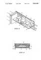
- FIG. 1is a perspective view illustrating first embodiment of the present invention
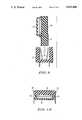
- FIG. 2is an expanded sectional view of the imaging element of FIG. 1;
- FIG. 3is an expanded sectional view similar to FIG. 2 illustrating a second embodiment of the present invention
- FIG. 4is an expanded sectional view illustrating an imaging element of a third embodiment of the present invention.
- FIG. 5is a perspective view illustrating a fourth embodiment of the present invention.
- FIG. 6is an expanded sectional view illustrating an imaging element of a fifth embodiment of the present invention.
- FIG. 7is an expanded sectional view illustrating an imaging element of a sixth embodiment of the present invention.
- FIG. 8is an expanded sectional view illustrating an imaging element of a seventh embodiment of the present invention.
- FIG. 9is an expanded sectional view illustrating an imaging element of the present invention.
- FIG. 10is an expanded sectional view illustrating an imaging element of a ninth embodiment of the present invention.
- FIG. 11is a sectional view illustrating a conventional solid state imaging device.
- FIGS. 1 and 2illustrate a first embodiment of the present invention.
- a solid state imaging element 10is disposed with its light receiving plane facing toward an object being observed. Thus, the element 10 can directly receive incident light (shown by the arrows).
- An FPC 11is provided on the side of the solid state imaging element 10.
- Wiring patterns 12are formed on the surface of the FPC 11.
- Plural chip components 13, e.g., a noise reduction circuit and a high frequency amplification circuit,are provided on the FPC 11 with wiring patterns 12 thereon.
- Connection pads 15are formed on an end portion 14 of the FPC. Extension cables 16 are connected to these connection pads 15.
- the surface of the FPC 11is covered by a protection film 24 made of polyimide resin.
- the solid state imaging element 10includes a CCD chip 17 and a light transparent cover 18 made of optical glass.
- the chip 17 and the cover 18are connected by connection bumps 19.
- Connection bumps 19are formed of solder, and In-Sn-Pb alloy is used in this embodiment.
- Connection bumps 19are formed using a thermocompression bonding technique with alloy balls of 100 ⁇ m in diameter. These balls are bonded to Al pads provided on the surface of the CCD chip 17.
- Electrode patterns 20are formed on the surface of the light transparent cover 18 using an evaporation technique. These electrode patterns 20 extend to a side surface 21 of the light transparent cover 18.
- the light transparent cover 18is made of optical glass having an efficiency to pass almost 100 % visible light in the visible region.
- the CCD chip 17 and the light transparent cover 18are thermocompression bonded after positioning the connection pads 19 and the electrode patterns 20.
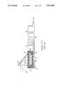
- the electrode patterns 20extend along the side surface 21 of the light transparent cover 18 and wiring patterns 12 provided on the surface of the FPC 11 are connected electrically and mechanically using an anisotropic electro-conductive film 23.
- the anisotropic electro-conductive film 23is made by diffusing subminiaturized metal balls into the thermoplastic resin.
- the anisotropic electro-conductive film 23is disposed between the side surface 21 of the light transparent cover 18 and the FPC 11, and is compression bonded at 180° C.
- electrode patterns 20 and wiring patterns 12are electrically connected through miniaturized metal balls diffused into the thermoplastic resin.
- the remaining parts of the light transparent cover 18 and the FPC 11 other than electrode patterns 20 and wiring patterns 12are connected only mechanically, because the metal balls do not contact therebetween, as compared with above-mentioned electrical connection.
- the solid state imaging element 10has been turned directly toward the object being observed without the need to bend the FPC 11. Furthermore, chip components 13 have been provided in the rear space of the solid state imaging element 10.
- Electrode pads of the CCD chip 17have been directly connected to electrode patterns 20 of the light transparent cover 18 through connection bumps 19. Thus, wire bonding has become unnecessary. As a result, parts of pads for bonding and parts for fixing the CCD chip and the light transparent cover have become unnecessary.
- FIG. 3shows a second embodiment of the present invention.
- first and second FPCs 25 and 26are connected on both sides of the light transparent cover 18 using first and second anisotropic electro-conductive films 27 and 28. This construction is useful when many chip components are assembled.
- FIG. 4shows a third embodiment of the present invention.
- connection bumpshave a double layer construction. Namely, bumps 29 are formed on the CCD chip 17 using the wire bonding method. In family bumps 30 are formed on the light transparent cover 18. Thereafter, both bumps 29 and 30 are connected using the thermocompression bonding technique. This construction makes the connection between patterns of the CCD chip or the light transparent cover and the connection bumps easier
- FIG. 5shows a fourth embodiment of the present invention.
- a first FPC 31 having wiring patterns 12 formed thereonis connected on the side of the solid state imaging element 10.
- a second FPC 32 assembled to the first FPC 31meets the FPC 31 at a right angles. Namely, chip components 13 assembled on the second FPC 32 are connected by soldering on wiring patterns of the first FPC 31. In the other words, chip components 13 are strongly joined face to face to both FPCs 31 and 32.
- chip components 13are assembled only on the one surface of the second FPC 32. However, these components may be assembled on both surfaces of the second FPC 32 when many components must be assembled thereon. Furthermore, in above-mentioned embodiment, only the second FPC 32 joins at a right angle to first FPC 31. However, this configuration may be modified, and several FPC's may be utilized.
- FIG. 6shows a fifth embodiment of the present invention.
- Tip portions bent 90 degrees of the leads 34 made of phosphor bronzeare fixed on electrode patterns 20 provided on the surface of the light transparent cover 18.
- the back surface of the CCD chip 17is sealed to the inside of leads 34 using an adhesive agent formed by a thermosetting resin into of an epoxy group.
- a ready-made socketis avarable, and its leads can be soldered directly on the printed circuit board.
- FIG. 7shows a sixth embodiment of the present invention. It is different to than the above-mentioned embodiment in that the tip portions of the leads are bent in two steps. As a result, the device is formed the flat-package type. In this device, leads 34 can be soldered directly on the printed circuit board too.
- FIG. 8shows a seventh embodiment of the present invention.
- Leads 34are bent surrounding from the side to top surfaces of the light transparent cover 18. This construction is strong mechanically. Further, this device can be used inserting directly into the socket having spring like leads 36.
- FIG. 9shows an eighth embodiment of the present invention. Leads 34 are provided only on the one side of the light transparent cover 18. This type device is easy to especially change the device from the socket.
- FIG. 10shows a ninth embodiment of the present invention. Electrode patterns 20 are extended until the both side surfaces of the light transparent cover 18, and leads 34 are connected to electrode patterns 20 on the side surfaces of the light transparent cover 18.
Landscapes
- Health & Medical Sciences (AREA)
- Life Sciences & Earth Sciences (AREA)
- Surgery (AREA)
- Engineering & Computer Science (AREA)
- Radiology & Medical Imaging (AREA)
- Heart & Thoracic Surgery (AREA)
- Biophysics (AREA)
- Nuclear Medicine, Radiotherapy & Molecular Imaging (AREA)
- Optics & Photonics (AREA)
- Pathology (AREA)
- Veterinary Medicine (AREA)
- Public Health (AREA)
- Biomedical Technology (AREA)
- Physics & Mathematics (AREA)
- Medical Informatics (AREA)
- Molecular Biology (AREA)
- Animal Behavior & Ethology (AREA)
- General Health & Medical Sciences (AREA)
- Multimedia (AREA)
- Signal Processing (AREA)
- Solid State Image Pick-Up Elements (AREA)
Abstract
Description
Claims (8)
Applications Claiming Priority (6)
| Application Number | Priority Date | Filing Date | Title |
|---|---|---|---|
| JP62318664AJPH01161775A (en) | 1987-12-18 | 1987-12-18 | solid state imaging device |
| JP62-318664 | 1987-12-18 | ||
| JP62318666AJPH01161979A (en) | 1987-12-18 | 1987-12-18 | Solid-state image pickup device |
| JP62-318665 | 1987-12-18 | ||
| JP62-318666 | 1987-12-18 | ||
| JP62318665AJP2582822B2 (en) | 1987-12-18 | 1987-12-18 | Circuit board |
Publications (1)
| Publication Number | Publication Date |
|---|---|
| US5021888Atrue US5021888A (en) | 1991-06-04 |
Family
ID=27339676
Family Applications (1)
| Application Number | Title | Priority Date | Filing Date |
|---|---|---|---|
| US07/284,610Expired - LifetimeUS5021888A (en) | 1987-12-18 | 1988-12-15 | Miniaturized solid state imaging device |
Country Status (1)
| Country | Link |
|---|---|
| US (1) | US5021888A (en) |
Cited By (105)
| Publication number | Priority date | Publication date | Assignee | Title |
|---|---|---|---|---|
| EP0475370A3 (en)* | 1990-09-10 | 1992-06-10 | Kabushiki Kaisha Toshiba | Compact imaging apparatus for electronic endoscope with improved optical characteristics |
| US5365268A (en)* | 1991-04-26 | 1994-11-15 | Fuji Photo Optical Co., Ltd. | Circuit board of solid-state image sensor for electronic endoscope |
| US5418566A (en)* | 1990-09-10 | 1995-05-23 | Kabushiki Kaisha Toshiba | Compact imaging apparatus for electronic endoscope with improved optical characteristics |
| US5448114A (en)* | 1992-07-15 | 1995-09-05 | Kabushiki Kaisha Toshiba | Semiconductor flipchip packaging having a perimeter wall |
| US5506401A (en)* | 1993-05-28 | 1996-04-09 | Kabushiki Kaisha Toshiba | Photoelectric converting device mounting apparatus with anisotropically conductive film for connecting leads of wiring board and electrode pads of photoelectric converting device and fabrication method thereof |
| US5534725A (en)* | 1992-06-16 | 1996-07-09 | Goldstar Electron Co., Ltd. | Resin molded charge coupled device package and method for preparation thereof |
| WO1996039916A1 (en) | 1995-06-07 | 1996-12-19 | Vista Medical Technologies, Inc. | Asymmetric stereo-optic endoscope |
| WO1997037583A1 (en) | 1996-04-05 | 1997-10-16 | Vista Medical Technologies, Inc. | A device for carrying two units in end to end disposition and for moving one of the units alongside the other of the units |
| FR2751197A1 (en)* | 1996-07-18 | 1998-01-23 | Tokendo Sarl | Video endoscope remote probe device for medical and industrial applications |
| US5754313A (en)* | 1996-07-17 | 1998-05-19 | Welch Allyn, Inc. | Imager assembly |
| US5763943A (en)* | 1996-01-29 | 1998-06-09 | International Business Machines Corporation | Electronic modules with integral sensor arrays |
| GB2321132A (en)* | 1997-01-13 | 1998-07-15 | Asahi Optical Co Ltd | Endoscope |
| US5896166A (en)* | 1993-06-02 | 1999-04-20 | Envision Medical Corporation | Remote CCD video camera with non-volatile digital memory |
| US5984861A (en)* | 1997-09-29 | 1999-11-16 | Boston Scientific Corporation | Endofluorescence imaging module for an endoscope |
| US6020646A (en)* | 1997-12-05 | 2000-02-01 | The Charles Stark Draper Laboratory, Inc. | Intergrated circuit die assembly |
| US6096065A (en)* | 1997-09-29 | 2000-08-01 | Boston Scientific Corporation | Sheath for tissue spectroscopy |
| US6119031A (en)* | 1996-11-21 | 2000-09-12 | Boston Scientific Corporation | Miniature spectrometer |
| EP1039268A1 (en)* | 1999-03-26 | 2000-09-27 | C.S.E.M. Centre Suisse D'electronique Et De Microtechnique Sa | Multi-sensor monitoring apparatus |
| FR2793019A1 (en)* | 1999-04-30 | 2000-11-03 | Suisse Electronique Microtech | MULTI-SENSOR MONITORING SYSTEM |
| US6185443B1 (en) | 1997-09-29 | 2001-02-06 | Boston Scientific Corporation | Visible display for an interventional device |
| US20010003800A1 (en)* | 1996-11-21 | 2001-06-14 | Steven J. Frank | Interventional photonic energy emitter system |
| US6289229B1 (en) | 1998-01-20 | 2001-09-11 | Scimed Life Systems, Inc. | Readable probe array for in vivo use |
| US6324418B1 (en) | 1997-09-29 | 2001-11-27 | Boston Scientific Corporation | Portable tissue spectroscopy apparatus and method |
| US20010055073A1 (en)* | 2000-06-16 | 2001-12-27 | Kohji Shinomiya | Solid state imaging apparatus |
| US6405073B1 (en) | 1997-07-22 | 2002-06-11 | Scimed Life Systems, Inc. | Miniature spectrometer system and method |
| US6417885B1 (en)* | 1995-08-30 | 2002-07-09 | Matsushita Electric Industrial Co., Ltd. | Solid-state image pickup device with a separable circuit board |
| US20020122583A1 (en)* | 2000-09-11 | 2002-09-05 | Thompson Robert Lee | System and method for obtaining and utilizing maintenance information |
| US6577339B1 (en) | 1997-07-30 | 2003-06-10 | Pinotage, Llc | Aircraft monitoring and analysis system and method |
| US20030194793A1 (en)* | 1997-03-31 | 2003-10-16 | Genentech, Inc. | Secreted and transmembrane polypeptides and nucleic acids encoding the same |
| US20030215128A1 (en)* | 2001-09-12 | 2003-11-20 | Pinotage Llc | System and method for obtaining and utilizing maintenance information |
| US20030220574A1 (en)* | 2002-03-18 | 2003-11-27 | Sarcos Investments Lc. | Miniaturized imaging device including utility aperture and SSID |
| US20030222325A1 (en)* | 2002-03-18 | 2003-12-04 | Sarcos Investments Lc. | Miniaturized imaging device with integrated circuit connector system |
| KR100410946B1 (en)* | 2001-05-16 | 2003-12-18 | 삼성전기주식회사 | Image sensor module and manufacturing method for the same |
| US20040171914A1 (en)* | 2001-06-18 | 2004-09-02 | Dov Avni | In vivo sensing device with a circuit board having rigid sections and flexible sections |
| US20050068432A1 (en)* | 1997-10-06 | 2005-03-31 | Canon Kabushiki Kaisha | Image sensor and method for driving an image sensor for reducing fixed pattern noise |
| US20050129108A1 (en)* | 2003-01-29 | 2005-06-16 | Everest Vit, Inc. | Remote video inspection system |
| US20050167773A1 (en)* | 2004-01-30 | 2005-08-04 | Kabushiki Kaisha Toshiba | Semiconductor element for solid state image sensing device and solid state image sensing device using the same |
| US20050190290A1 (en)* | 2004-03-01 | 2005-09-01 | Cheng-Kuang Sun | Camera module |
| US20050200978A1 (en)* | 2004-03-11 | 2005-09-15 | Pinotage, L.L.C. | Lens assembly and optical imaging using same |
| US20050218495A1 (en)* | 1990-09-24 | 2005-10-06 | Tessera, Inc. | Microelectronic assembly having encapsulated wire bonding leads |
| US20050267328A1 (en)* | 2002-05-16 | 2005-12-01 | C2Cure Inc. | Miniature camera head |
| US6977685B1 (en) | 1999-02-26 | 2005-12-20 | Massachusetts Institute Of Technology | Single-chip imager system with programmable dynamic range |
| US20060004256A1 (en)* | 2002-09-30 | 2006-01-05 | Zvika Gilad | Reduced size imaging device |
| US20060146172A1 (en)* | 2002-03-18 | 2006-07-06 | Jacobsen Stephen C | Miniaturized utility device having integrated optical capabilities |
| US20060164510A1 (en)* | 2005-01-24 | 2006-07-27 | Doron Adler | Sensor with narrow mounting profile |
| US20070118012A1 (en)* | 2005-11-23 | 2007-05-24 | Zvika Gilad | Method of assembling an in-vivo imaging device |
| US20070195187A1 (en)* | 2006-02-23 | 2007-08-23 | Hiromi Tagata | Image pickup apparatus and image pickup unit |
| US20080045788A1 (en)* | 2002-11-27 | 2008-02-21 | Zvika Gilad | Method and device of imaging with an in vivo imager |
| EP1486077A4 (en)* | 2002-03-18 | 2008-03-26 | Sarcos Invest Lc | Miniaturized imaging device |
| DE19816309B4 (en)* | 1997-04-14 | 2008-04-03 | CiS Institut für Mikrosensorik gGmbH | Method for direct mounting of silicon sensors and sensors manufactured thereafter |
| EP1989996A1 (en)* | 2007-05-10 | 2008-11-12 | Stmicroelectronics SA | Exploration of a cavity with an image sensor |
| FR2916084A1 (en)* | 2007-05-10 | 2008-11-14 | St Microelectronics Sa | Cavity exploration device head manufacturing method for endoscope, involves soldering micro-cable on pellets, adhering micro-cable, and molding micro-cable on pellets using resin layers that completely cover unrolled part of micro-cable |
| US20080304143A1 (en)* | 2007-06-05 | 2008-12-11 | Jacobsen Stephen C | Mini-scope for multi-directional imaging |
| US20090054764A1 (en)* | 2000-04-10 | 2009-02-26 | C2Cure, Inc. | Three-dimensional image reconstruction using two light sources |
| EP2074930A1 (en)* | 2007-12-27 | 2009-07-01 | FUJIFILM Corporation | Electronic endoscope |
| WO2009086901A1 (en)* | 2008-01-11 | 2009-07-16 | Knorr-Bremse Systeme für Nutzfahrzeuge GmbH | Conductor track carrier and method for the production of a conductor track carrier |
| US20090180197A1 (en)* | 2008-01-11 | 2009-07-16 | Sterling Lc | Grin lens microscope system |
| US7588535B2 (en) | 2001-12-11 | 2009-09-15 | C2Cure Inc. | Apparatus, method and system for intravascular photographic imaging |
| US20090287137A1 (en)* | 1996-11-21 | 2009-11-19 | Boston Scientific Corporation | Mucosal ablation |
| EP2144273A1 (en)* | 2008-07-10 | 2010-01-13 | ITT Manufacturing Enterprises, Inc. | Electrical connection of a substrate within a vacuum device via electrically conductive epoxy/paste |
| US20100022831A1 (en)* | 2008-07-22 | 2010-01-28 | Zhang Zifeng | Endoscope and a Method of Manufacturing the Same |
| US7758499B2 (en) | 2001-08-10 | 2010-07-20 | C2Cure, Inc. | Method and apparatus for viewing through blood |
| US20100326703A1 (en)* | 2009-06-24 | 2010-12-30 | Zvika Gilad | In vivo sensing device with a flexible circuit board and method of assembly thereof |
| US20110249106A1 (en)* | 2010-04-07 | 2011-10-13 | Olympus Corporation | Image pickup apparatus, endoscope and manufacturing method for image pickup apparatus |
| US20110295064A1 (en)* | 2009-06-25 | 2011-12-01 | Olympus Medical Systems Corp. | Image pickup unit |
| EP1845835A4 (en)* | 2005-01-27 | 2012-03-21 | Super Dimension Ltd | Endoscope with miniature imaging arrangement |
| EP2434748A1 (en)* | 2010-09-27 | 2012-03-28 | Karl Storz GmbH & Co. KG | Image capturing module and method for manufacturing the same |
| US8213676B2 (en) | 2006-12-20 | 2012-07-03 | Ge Inspection Technologies Lp | Inspection apparatus method and apparatus comprising motion responsive control |
| US8328877B2 (en) | 2002-03-19 | 2012-12-11 | Boston Scientific Scimed, Inc. | Stent retention element and related methods |
| US8486735B2 (en) | 2008-07-30 | 2013-07-16 | Raytheon Company | Method and device for incremental wavelength variation to analyze tissue |
| JP2013176487A (en)* | 2012-02-29 | 2013-09-09 | Fujifilm Corp | Terminal connecting unit and method for connecting terminal |
| US8614768B2 (en) | 2002-03-18 | 2013-12-24 | Raytheon Company | Miniaturized imaging device including GRIN lens optically coupled to SSID |
| US8663088B2 (en) | 2003-09-15 | 2014-03-04 | Covidien Lp | System of accessories for use with bronchoscopes |
| US8690762B2 (en) | 2008-06-18 | 2014-04-08 | Raytheon Company | Transparent endoscope head defining a focal length |
| US8717428B2 (en) | 2009-10-01 | 2014-05-06 | Raytheon Company | Light diffusion apparatus |
| US8764725B2 (en) | 2004-02-09 | 2014-07-01 | Covidien Lp | Directional anchoring mechanism, method and applications thereof |
| US8810636B2 (en) | 2006-12-20 | 2014-08-19 | Ge Inspection Technologies, Lp | Inspection apparatus method and apparatus comprising selective frame output |
| US8828028B2 (en) | 2009-11-03 | 2014-09-09 | Raytheon Company | Suture device and method for closing a planar opening |
| US8885034B2 (en) | 1997-10-06 | 2014-11-11 | Micro-Imaging Solutions Llc | Reduced area imaging device incorporated within endoscopic devices |
| US8905920B2 (en) | 2007-09-27 | 2014-12-09 | Covidien Lp | Bronchoscope adapter and method |
| EP2720454A4 (en)* | 2011-06-13 | 2015-01-28 | Olympus Corp | IMAGE CAPTURE DEVICE AND ELECTRONIC APPARATUS EMPLOYING THE SAME |
| US8952312B2 (en) | 2011-05-12 | 2015-02-10 | Olive Medical Corporation | Image sensor for endoscopic use |
| US9055881B2 (en) | 2004-04-26 | 2015-06-16 | Super Dimension Ltd. | System and method for image-based alignment of an endoscope |
| US9060704B2 (en) | 2008-11-04 | 2015-06-23 | Sarcos Lc | Method and device for wavelength shifted imaging |
| US20150190039A1 (en)* | 2013-06-28 | 2015-07-09 | Olympus Medical Systems Corp. | Imaging module and endoscope device |
| US9144664B2 (en) | 2009-10-01 | 2015-09-29 | Sarcos Lc | Method and apparatus for manipulating movement of a micro-catheter |
| US9257763B2 (en) | 2013-07-02 | 2016-02-09 | Gyrus Acmi, Inc. | Hybrid interconnect |
| US20160106303A1 (en)* | 2014-10-16 | 2016-04-21 | Dashiell A. Birnkrant | Focusable Camera Module For Endoscopes |
| US9462234B2 (en) | 2012-07-26 | 2016-10-04 | DePuy Synthes Products, Inc. | Camera system with minimal area monolithic CMOS image sensor |
| US9510739B2 (en) | 2013-07-12 | 2016-12-06 | Gyrus Acmi, Inc. | Endoscope small imaging system |
| US9516239B2 (en) | 2012-07-26 | 2016-12-06 | DePuy Synthes Products, Inc. | YCBCR pulsed illumination scheme in a light deficient environment |
| US9641815B2 (en) | 2013-03-15 | 2017-05-02 | DePuy Synthes Products, Inc. | Super resolution and color motion artifact correction in a pulsed color imaging system |
| US9661996B2 (en) | 2009-10-01 | 2017-05-30 | Sarcos Lc | Needle delivered imaging device |
| US9777913B2 (en) | 2013-03-15 | 2017-10-03 | DePuy Synthes Products, Inc. | Controlling the integral light energy of a laser pulse |
| US10084944B2 (en) | 2014-03-21 | 2018-09-25 | DePuy Synthes Products, Inc. | Card edge connector for an imaging sensor |
| US10251530B2 (en) | 2013-03-15 | 2019-04-09 | DePuy Synthes Products, Inc. | Scope sensing in a light controlled environment |
| US10291850B2 (en) | 2006-12-20 | 2019-05-14 | General Electric Company | Inspection apparatus method and apparatus comprising selective frame output |
| US10485404B2 (en) | 2016-03-01 | 2019-11-26 | Karl Storz Endovision, Inc. | Compact image sensor module and method of assembly for image sensor modules |
| US10517469B2 (en) | 2013-03-15 | 2019-12-31 | DePuy Synthes Products, Inc. | Image sensor synchronization without input clock and data transmission clock |
| US10561302B2 (en) | 2013-03-15 | 2020-02-18 | DePuy Synthes Products, Inc. | Viewing trocar with integrated prism for use with angled endoscope |
| US10568496B2 (en) | 2012-07-26 | 2020-02-25 | DePuy Synthes Products, Inc. | Continuous video in a light deficient environment |
| US10582834B2 (en) | 2010-06-15 | 2020-03-10 | Covidien Lp | Locatable expandable working channel and method |
| US10750933B2 (en) | 2013-03-15 | 2020-08-25 | DePuy Synthes Products, Inc. | Minimize image sensor I/O and conductor counts in endoscope applications |
| US10952593B2 (en) | 2014-06-10 | 2021-03-23 | Covidien Lp | Bronchoscope adapter |
| US12301970B2 (en)* | 2021-06-16 | 2025-05-13 | Olympus Corporation | Image pickup unit and endoscope |
Citations (5)
| Publication number | Priority date | Publication date | Assignee | Title |
|---|---|---|---|---|
| US4660277A (en)* | 1984-06-22 | 1987-04-28 | Fuji Xerox Co. Ltd. | Method for forming large area amorphous semiconductor layer and contact type image sensor |
| US4684974A (en)* | 1984-11-16 | 1987-08-04 | Matsushita Electric Industrial Co. Ltd. | Electrode connection structure of flat device |
| JPS62281361A (en)* | 1986-05-29 | 1987-12-07 | Matsushita Electric Ind Co Ltd | Semiconductor device |
| US4779130A (en)* | 1985-01-14 | 1988-10-18 | Olympus Optical Co., Ltd. | Endoscope having a solid-state image sensor and shield therefor |
| US4831456A (en)* | 1986-12-08 | 1989-05-16 | Olympus Optical Co., Ltd. | Imaging apparatus using a solid-state imaging element having a substrate |
- 1988
- 1988-12-15USUS07/284,610patent/US5021888A/ennot_activeExpired - Lifetime
Patent Citations (5)
| Publication number | Priority date | Publication date | Assignee | Title |
|---|---|---|---|---|
| US4660277A (en)* | 1984-06-22 | 1987-04-28 | Fuji Xerox Co. Ltd. | Method for forming large area amorphous semiconductor layer and contact type image sensor |
| US4684974A (en)* | 1984-11-16 | 1987-08-04 | Matsushita Electric Industrial Co. Ltd. | Electrode connection structure of flat device |
| US4779130A (en)* | 1985-01-14 | 1988-10-18 | Olympus Optical Co., Ltd. | Endoscope having a solid-state image sensor and shield therefor |
| JPS62281361A (en)* | 1986-05-29 | 1987-12-07 | Matsushita Electric Ind Co Ltd | Semiconductor device |
| US4831456A (en)* | 1986-12-08 | 1989-05-16 | Olympus Optical Co., Ltd. | Imaging apparatus using a solid-state imaging element having a substrate |
Cited By (225)
| Publication number | Priority date | Publication date | Assignee | Title |
|---|---|---|---|---|
| EP0475370A3 (en)* | 1990-09-10 | 1992-06-10 | Kabushiki Kaisha Toshiba | Compact imaging apparatus for electronic endoscope with improved optical characteristics |
| US5418566A (en)* | 1990-09-10 | 1995-05-23 | Kabushiki Kaisha Toshiba | Compact imaging apparatus for electronic endoscope with improved optical characteristics |
| US20050218495A1 (en)* | 1990-09-24 | 2005-10-06 | Tessera, Inc. | Microelectronic assembly having encapsulated wire bonding leads |
| US5365268A (en)* | 1991-04-26 | 1994-11-15 | Fuji Photo Optical Co., Ltd. | Circuit board of solid-state image sensor for electronic endoscope |
| US5534725A (en)* | 1992-06-16 | 1996-07-09 | Goldstar Electron Co., Ltd. | Resin molded charge coupled device package and method for preparation thereof |
| US5448114A (en)* | 1992-07-15 | 1995-09-05 | Kabushiki Kaisha Toshiba | Semiconductor flipchip packaging having a perimeter wall |
| US5506401A (en)* | 1993-05-28 | 1996-04-09 | Kabushiki Kaisha Toshiba | Photoelectric converting device mounting apparatus with anisotropically conductive film for connecting leads of wiring board and electrode pads of photoelectric converting device and fabrication method thereof |
| US5786589A (en)* | 1993-05-28 | 1998-07-28 | Kabushiki Kaisha Toshiba | Photoelectric converting device with anisotropically conductive film for connecting leads of wiring board and electrode pads of photoelectric converting device |
| US5896166A (en)* | 1993-06-02 | 1999-04-20 | Envision Medical Corporation | Remote CCD video camera with non-volatile digital memory |
| US6313868B1 (en) | 1993-06-02 | 2001-11-06 | Linvatec Corporation | Remote CCD video camera with non-volatile digital memory |
| WO1996039916A1 (en) | 1995-06-07 | 1996-12-19 | Vista Medical Technologies, Inc. | Asymmetric stereo-optic endoscope |
| US6417885B1 (en)* | 1995-08-30 | 2002-07-09 | Matsushita Electric Industrial Co., Ltd. | Solid-state image pickup device with a separable circuit board |
| US5763943A (en)* | 1996-01-29 | 1998-06-09 | International Business Machines Corporation | Electronic modules with integral sensor arrays |
| US5907178A (en)* | 1996-01-29 | 1999-05-25 | International Business Machines Corporation | Multi-view imaging apparatus |
| US5869896A (en)* | 1996-01-29 | 1999-02-09 | International Business Machines Corporation | Packaged electronic module and integral sensor array |
| US5782752A (en)* | 1996-04-05 | 1998-07-21 | Vista Medical Technologies, Inc. | Device for carrying two units in end to end disposition and for moving one of the units alongside the other of the units |
| WO1997037583A1 (en) | 1996-04-05 | 1997-10-16 | Vista Medical Technologies, Inc. | A device for carrying two units in end to end disposition and for moving one of the units alongside the other of the units |
| US5754313A (en)* | 1996-07-17 | 1998-05-19 | Welch Allyn, Inc. | Imager assembly |
| FR2751197A1 (en)* | 1996-07-18 | 1998-01-23 | Tokendo Sarl | Video endoscope remote probe device for medical and industrial applications |
| US6343227B1 (en) | 1996-11-21 | 2002-01-29 | Boston Scientific Corporation | Miniature spectrometer |
| US6119031A (en)* | 1996-11-21 | 2000-09-12 | Boston Scientific Corporation | Miniature spectrometer |
| US20020115918A1 (en)* | 1996-11-21 | 2002-08-22 | Crowley Robert J. | Miniature spectrometer |
| US8660637B2 (en) | 1996-11-21 | 2014-02-25 | Boston Scientific Scimed, Inc. | Miniature spectrometer |
| US20090287137A1 (en)* | 1996-11-21 | 2009-11-19 | Boston Scientific Corporation | Mucosal ablation |
| US8126531B2 (en) | 1996-11-21 | 2012-02-28 | Boston Scientific Scimed, Inc. | Miniature spectrometer |
| US20080114419A1 (en)* | 1996-11-21 | 2008-05-15 | Boston Scientific Corporation | Interventional photonic energy emitter system |
| US20010003800A1 (en)* | 1996-11-21 | 2001-06-14 | Steven J. Frank | Interventional photonic energy emitter system |
| GB2321132B (en)* | 1997-01-13 | 2002-04-17 | Asahi Optical Co Ltd | Electronic endoscope |
| US6142930A (en)* | 1997-01-13 | 2000-11-07 | Asahi Kogaku Kogyo Kabushiki Kaisha | Electronic endoscope having compact construction |
| GB2321132A (en)* | 1997-01-13 | 1998-07-15 | Asahi Optical Co Ltd | Endoscope |
| US20030194793A1 (en)* | 1997-03-31 | 2003-10-16 | Genentech, Inc. | Secreted and transmembrane polypeptides and nucleic acids encoding the same |
| DE19816309B4 (en)* | 1997-04-14 | 2008-04-03 | CiS Institut für Mikrosensorik gGmbH | Method for direct mounting of silicon sensors and sensors manufactured thereafter |
| US6405073B1 (en) | 1997-07-22 | 2002-06-11 | Scimed Life Systems, Inc. | Miniature spectrometer system and method |
| US6577339B1 (en) | 1997-07-30 | 2003-06-10 | Pinotage, Llc | Aircraft monitoring and analysis system and method |
| US6744467B2 (en) | 1997-07-30 | 2004-06-01 | Pinotage, Llc | Lens system for camera |
| US20040218083A1 (en)* | 1997-07-30 | 2004-11-04 | Pinotage L.L.C., An Arkansas Corporation | Lens assembly |
| US6324418B1 (en) | 1997-09-29 | 2001-11-27 | Boston Scientific Corporation | Portable tissue spectroscopy apparatus and method |
| US6364831B1 (en) | 1997-09-29 | 2002-04-02 | Boston Scientific Corporation | Endofluorescence imaging module for an endoscope |
| US5984861A (en)* | 1997-09-29 | 1999-11-16 | Boston Scientific Corporation | Endofluorescence imaging module for an endoscope |
| US6882875B1 (en) | 1997-09-29 | 2005-04-19 | Boston Scientific Corporation | Visible display for an interventional device |
| US6383209B1 (en) | 1997-09-29 | 2002-05-07 | Boston Scientific Corporation | Sheath for tissue spectroscopy |
| US6096065A (en)* | 1997-09-29 | 2000-08-01 | Boston Scientific Corporation | Sheath for tissue spectroscopy |
| US6185443B1 (en) | 1997-09-29 | 2001-02-06 | Boston Scientific Corporation | Visible display for an interventional device |
| US6950132B1 (en)* | 1997-10-06 | 2005-09-27 | Canon Kabushiki Kaisha | Image sensor and method for driving an image sensor for reducing fixed pattern noise |
| US9307895B2 (en) | 1997-10-06 | 2016-04-12 | Micro-Imaging Solutions, Llc | Reduced area imaging device incorporated within endoscopic devices |
| US9198565B2 (en) | 1997-10-06 | 2015-12-01 | Micro-Imaging Solutions | Reduced area imaging device incorporated within endoscopic devices |
| US9186052B1 (en) | 1997-10-06 | 2015-11-17 | Micro-Imagaing Solutions | Reduced area imaging device incorporated within endoscopic devices |
| US9667896B2 (en) | 1997-10-06 | 2017-05-30 | Cellect Llc | Reduced area imaging device incorporated within endoscopic devices |
| US8885034B2 (en) | 1997-10-06 | 2014-11-11 | Micro-Imaging Solutions Llc | Reduced area imaging device incorporated within endoscopic devices |
| US20050068432A1 (en)* | 1997-10-06 | 2005-03-31 | Canon Kabushiki Kaisha | Image sensor and method for driving an image sensor for reducing fixed pattern noise |
| US6204090B1 (en)* | 1997-12-05 | 2001-03-20 | The Charles Stark Draper Laboratory, Inc. | Method for attaching a die to a carrier utilizing an electrically nonconductive layer |
| US6020646A (en)* | 1997-12-05 | 2000-02-01 | The Charles Stark Draper Laboratory, Inc. | Intergrated circuit die assembly |
| US6289229B1 (en) | 1998-01-20 | 2001-09-11 | Scimed Life Systems, Inc. | Readable probe array for in vivo use |
| US7302289B2 (en) | 1998-01-20 | 2007-11-27 | Scimed Life Systems, Inc. | Readable probe array for in-vivo use |
| US8140148B2 (en) | 1998-01-20 | 2012-03-20 | Boston Scientific Scimed Ltd. | Readable probe array for in vivo use |
| US6977685B1 (en) | 1999-02-26 | 2005-12-20 | Massachusetts Institute Of Technology | Single-chip imager system with programmable dynamic range |
| EP1039268A1 (en)* | 1999-03-26 | 2000-09-27 | C.S.E.M. Centre Suisse D'electronique Et De Microtechnique Sa | Multi-sensor monitoring apparatus |
| FR2793019A1 (en)* | 1999-04-30 | 2000-11-03 | Suisse Electronique Microtech | MULTI-SENSOR MONITORING SYSTEM |
| US7559892B2 (en) | 2000-04-10 | 2009-07-14 | C2Cure, Inc. | Medical wireless imaging device |
| US20090054764A1 (en)* | 2000-04-10 | 2009-02-26 | C2Cure, Inc. | Three-dimensional image reconstruction using two light sources |
| US20060181638A1 (en)* | 2000-06-16 | 2006-08-17 | Mitsubishi Denki Kabushiki Kaisha | Solid state imaging apparatus |
| US7190404B2 (en) | 2000-06-16 | 2007-03-13 | Renesas Technology Corp. | Solid state imaging apparatus |
| US7046296B2 (en)* | 2000-06-16 | 2006-05-16 | Renesas Technology Corp | Solid state imaging apparatus |
| US20010055073A1 (en)* | 2000-06-16 | 2001-12-27 | Kohji Shinomiya | Solid state imaging apparatus |
| US7633543B2 (en) | 2000-06-16 | 2009-12-15 | Renesas Technology Corp. | Solid state imaging apparatus |
| US20070126923A1 (en)* | 2000-06-16 | 2007-06-07 | Renesas Technology Corp. | Solid state imaging apparatus |
| US6529620B2 (en) | 2000-09-11 | 2003-03-04 | Pinotage, L.L.C. | System and method for obtaining and utilizing maintenance information |
| US7068301B2 (en) | 2000-09-11 | 2006-06-27 | Pinotage L.L.C. | System and method for obtaining and utilizing maintenance information |
| US20020122583A1 (en)* | 2000-09-11 | 2002-09-05 | Thompson Robert Lee | System and method for obtaining and utilizing maintenance information |
| KR100410946B1 (en)* | 2001-05-16 | 2003-12-18 | 삼성전기주식회사 | Image sensor module and manufacturing method for the same |
| US20040171914A1 (en)* | 2001-06-18 | 2004-09-02 | Dov Avni | In vivo sensing device with a circuit board having rigid sections and flexible sections |
| US7998065B2 (en) | 2001-06-18 | 2011-08-16 | Given Imaging Ltd. | In vivo sensing device with a circuit board having rigid sections and flexible sections |
| US7758499B2 (en) | 2001-08-10 | 2010-07-20 | C2Cure, Inc. | Method and apparatus for viewing through blood |
| US20030215128A1 (en)* | 2001-09-12 | 2003-11-20 | Pinotage Llc | System and method for obtaining and utilizing maintenance information |
| US7588535B2 (en) | 2001-12-11 | 2009-09-15 | C2Cure Inc. | Apparatus, method and system for intravascular photographic imaging |
| US20030220574A1 (en)* | 2002-03-18 | 2003-11-27 | Sarcos Investments Lc. | Miniaturized imaging device including utility aperture and SSID |
| US8614768B2 (en) | 2002-03-18 | 2013-12-24 | Raytheon Company | Miniaturized imaging device including GRIN lens optically coupled to SSID |
| US20080185672A1 (en)* | 2002-03-18 | 2008-08-07 | Jacobsen Stephen C | Miniaturized imaging device with integrated circuit connector system |
| US20030222325A1 (en)* | 2002-03-18 | 2003-12-04 | Sarcos Investments Lc. | Miniaturized imaging device with integrated circuit connector system |
| US7629659B2 (en) | 2002-03-18 | 2009-12-08 | Sterling Lc | Miniaturized imaging device with integrated circuit connector system |
| US7591780B2 (en) | 2002-03-18 | 2009-09-22 | Sterling Lc | Miniaturized imaging device with integrated circuit connector system |
| US20060146172A1 (en)* | 2002-03-18 | 2006-07-06 | Jacobsen Stephen C | Miniaturized utility device having integrated optical capabilities |
| EP1486077A4 (en)* | 2002-03-18 | 2008-03-26 | Sarcos Invest Lc | Miniaturized imaging device |
| US7787939B2 (en) | 2002-03-18 | 2010-08-31 | Sterling Lc | Miniaturized imaging device including utility aperture and SSID |
| US8328877B2 (en) | 2002-03-19 | 2012-12-11 | Boston Scientific Scimed, Inc. | Stent retention element and related methods |
| US8194121B2 (en) | 2002-05-16 | 2012-06-05 | C2Cure, Inc. | Miniature camera head |
| US20050267328A1 (en)* | 2002-05-16 | 2005-12-01 | C2Cure Inc. | Miniature camera head |
| US7662093B2 (en)* | 2002-09-30 | 2010-02-16 | Given Imaging, Ltd. | Reduced size imaging device |
| US20060004256A1 (en)* | 2002-09-30 | 2006-01-05 | Zvika Gilad | Reduced size imaging device |
| US20080045788A1 (en)* | 2002-11-27 | 2008-02-21 | Zvika Gilad | Method and device of imaging with an in vivo imager |
| US20050129108A1 (en)* | 2003-01-29 | 2005-06-16 | Everest Vit, Inc. | Remote video inspection system |
| US10383509B2 (en) | 2003-09-15 | 2019-08-20 | Covidien Lp | System of accessories for use with bronchoscopes |
| US8663088B2 (en) | 2003-09-15 | 2014-03-04 | Covidien Lp | System of accessories for use with bronchoscopes |
| US9089261B2 (en) | 2003-09-15 | 2015-07-28 | Covidien Lp | System of accessories for use with bronchoscopes |
| US20050167773A1 (en)* | 2004-01-30 | 2005-08-04 | Kabushiki Kaisha Toshiba | Semiconductor element for solid state image sensing device and solid state image sensing device using the same |
| US8764725B2 (en) | 2004-02-09 | 2014-07-01 | Covidien Lp | Directional anchoring mechanism, method and applications thereof |
| US20050190290A1 (en)* | 2004-03-01 | 2005-09-01 | Cheng-Kuang Sun | Camera module |
| US7663693B2 (en)* | 2004-03-01 | 2010-02-16 | United Microelectronics Corp. | Camera module |
| US20050200978A1 (en)* | 2004-03-11 | 2005-09-15 | Pinotage, L.L.C. | Lens assembly and optical imaging using same |
| US7050245B2 (en) | 2004-03-11 | 2006-05-23 | Pinotage L.L.C. | Lens assembly and optical imaging using same |
| US7054076B2 (en) | 2004-03-11 | 2006-05-30 | Pinotage, L.L.C. | Lens assembly and optical imaging system using same |
| US9055881B2 (en) | 2004-04-26 | 2015-06-16 | Super Dimension Ltd. | System and method for image-based alignment of an endoscope |
| US10321803B2 (en) | 2004-04-26 | 2019-06-18 | Covidien Lp | System and method for image-based alignment of an endoscope |
| US20060164510A1 (en)* | 2005-01-24 | 2006-07-27 | Doron Adler | Sensor with narrow mounting profile |
| WO2006077573A1 (en)* | 2005-01-24 | 2006-07-27 | C2Cure Inc. | Sensor with narrow mounting profile |
| EP1845835A4 (en)* | 2005-01-27 | 2012-03-21 | Super Dimension Ltd | Endoscope with miniature imaging arrangement |
| US20070118012A1 (en)* | 2005-11-23 | 2007-05-24 | Zvika Gilad | Method of assembling an in-vivo imaging device |
| US7750279B2 (en)* | 2006-02-23 | 2010-07-06 | Olympus Imaging Corp. | Image pickup apparatus and image pickup unit |
| US20070195187A1 (en)* | 2006-02-23 | 2007-08-23 | Hiromi Tagata | Image pickup apparatus and image pickup unit |
| US9621808B2 (en) | 2006-12-20 | 2017-04-11 | General Electric Company | Inspection apparatus method and apparatus comprising selective frame output |
| US8213676B2 (en) | 2006-12-20 | 2012-07-03 | Ge Inspection Technologies Lp | Inspection apparatus method and apparatus comprising motion responsive control |
| US10291850B2 (en) | 2006-12-20 | 2019-05-14 | General Electric Company | Inspection apparatus method and apparatus comprising selective frame output |
| US8810636B2 (en) | 2006-12-20 | 2014-08-19 | Ge Inspection Technologies, Lp | Inspection apparatus method and apparatus comprising selective frame output |
| US20080277673A1 (en)* | 2007-05-10 | 2008-11-13 | Stmicroelectronics S.A. | Cavity exploration with an image sensor |
| FR2916084A1 (en)* | 2007-05-10 | 2008-11-14 | St Microelectronics Sa | Cavity exploration device head manufacturing method for endoscope, involves soldering micro-cable on pellets, adhering micro-cable, and molding micro-cable on pellets using resin layers that completely cover unrolled part of micro-cable |
| EP1989996A1 (en)* | 2007-05-10 | 2008-11-12 | Stmicroelectronics SA | Exploration of a cavity with an image sensor |
| US9596981B2 (en) | 2007-05-10 | 2017-03-21 | Stmicroelectronics S.A. | Cavity exploration with an image sensor |
| US7835074B2 (en) | 2007-06-05 | 2010-11-16 | Sterling Lc | Mini-scope for multi-directional imaging |
| US8358462B2 (en) | 2007-06-05 | 2013-01-22 | Jacobsen Stephen C | Mini-scope for multi-directional imaging |
| US20080304143A1 (en)* | 2007-06-05 | 2008-12-11 | Jacobsen Stephen C | Mini-scope for multi-directional imaging |
| US9668639B2 (en) | 2007-09-27 | 2017-06-06 | Covidien Lp | Bronchoscope adapter and method |
| US8905920B2 (en) | 2007-09-27 | 2014-12-09 | Covidien Lp | Bronchoscope adapter and method |
| US9986895B2 (en) | 2007-09-27 | 2018-06-05 | Covidien Lp | Bronchoscope adapter and method |
| US10390686B2 (en) | 2007-09-27 | 2019-08-27 | Covidien Lp | Bronchoscope adapter and method |
| US10980400B2 (en) | 2007-09-27 | 2021-04-20 | Covidien Lp | Bronchoscope adapter and method |
| EP2074930A1 (en)* | 2007-12-27 | 2009-07-01 | FUJIFILM Corporation | Electronic endoscope |
| US20090177038A1 (en)* | 2007-12-27 | 2009-07-09 | Fujifilm Corporation | Electronic endoscope |
| US8161821B2 (en) | 2008-01-11 | 2012-04-24 | Knorr-Bremse Systeme Fuer Nutzfahrzeuge Gmbh | Conductor track carrier and method for the production of a conductor track carrier |
| US7969659B2 (en) | 2008-01-11 | 2011-06-28 | Sterling Lc | Grin lens microscope system |
| WO2009086901A1 (en)* | 2008-01-11 | 2009-07-16 | Knorr-Bremse Systeme für Nutzfahrzeuge GmbH | Conductor track carrier and method for the production of a conductor track carrier |
| US20090180197A1 (en)* | 2008-01-11 | 2009-07-16 | Sterling Lc | Grin lens microscope system |
| US20100313666A1 (en)* | 2008-01-11 | 2010-12-16 | Knorr Bremse Systeme Fuer Nutzfahrzeuge Gmbh | Conductor Track Carrier and Method for the Production of a Conductor Track Carrier |
| US8690762B2 (en) | 2008-06-18 | 2014-04-08 | Raytheon Company | Transparent endoscope head defining a focal length |
| US9521946B2 (en) | 2008-06-18 | 2016-12-20 | Sarcos Lc | Transparent endoscope head defining a focal length |
| EP2144273A1 (en)* | 2008-07-10 | 2010-01-13 | ITT Manufacturing Enterprises, Inc. | Electrical connection of a substrate within a vacuum device via electrically conductive epoxy/paste |
| US7956521B2 (en) | 2008-07-10 | 2011-06-07 | Itt Manufacturing Enterprises, Inc. | Electrical connection of a substrate within a vacuum device via electrically conductive epoxy/paste |
| US20100006765A1 (en)* | 2008-07-10 | 2010-01-14 | Itt Manufacturing Enterprises, Inc. | Electrical Connection Of A Substrate Within A Vacuum Device Via Electrically Conductive Epoxy/Paste |
| US20100022831A1 (en)* | 2008-07-22 | 2010-01-28 | Zhang Zifeng | Endoscope and a Method of Manufacturing the Same |
| US8216127B2 (en)* | 2008-07-22 | 2012-07-10 | BYD Company Ltd. | Endoscope and a method of manufacturing the same |
| US8486735B2 (en) | 2008-07-30 | 2013-07-16 | Raytheon Company | Method and device for incremental wavelength variation to analyze tissue |
| US9259142B2 (en) | 2008-07-30 | 2016-02-16 | Sarcos Lc | Method and device for incremental wavelength variation to analyze tissue |
| US9717418B2 (en) | 2008-11-04 | 2017-08-01 | Sarcos Lc | Method and device for wavelength shifted imaging |
| US9060704B2 (en) | 2008-11-04 | 2015-06-23 | Sarcos Lc | Method and device for wavelength shifted imaging |
| US20100326703A1 (en)* | 2009-06-24 | 2010-12-30 | Zvika Gilad | In vivo sensing device with a flexible circuit board and method of assembly thereof |
| US8516691B2 (en) | 2009-06-24 | 2013-08-27 | Given Imaging Ltd. | Method of assembly of an in vivo imaging device with a flexible circuit board |
| US9078579B2 (en) | 2009-06-24 | 2015-07-14 | Given Imaging Ltd. | In vivo sensing device with a flexible circuit board |
| US8821382B2 (en)* | 2009-06-25 | 2014-09-02 | Olympus Medical Systems Corp. | Image pickup unit |
| US20110295064A1 (en)* | 2009-06-25 | 2011-12-01 | Olympus Medical Systems Corp. | Image pickup unit |
| US8717428B2 (en) | 2009-10-01 | 2014-05-06 | Raytheon Company | Light diffusion apparatus |
| US9144664B2 (en) | 2009-10-01 | 2015-09-29 | Sarcos Lc | Method and apparatus for manipulating movement of a micro-catheter |
| US9661996B2 (en) | 2009-10-01 | 2017-05-30 | Sarcos Lc | Needle delivered imaging device |
| US8828028B2 (en) | 2009-11-03 | 2014-09-09 | Raytheon Company | Suture device and method for closing a planar opening |
| US20110249106A1 (en)* | 2010-04-07 | 2011-10-13 | Olympus Corporation | Image pickup apparatus, endoscope and manufacturing method for image pickup apparatus |
| US8698887B2 (en)* | 2010-04-07 | 2014-04-15 | Olympus Corporation | Image pickup apparatus, endoscope and manufacturing method for image pickup apparatus |
| US10582834B2 (en) | 2010-06-15 | 2020-03-10 | Covidien Lp | Locatable expandable working channel and method |
| US8633429B2 (en) | 2010-09-27 | 2014-01-21 | Karl Storz Gmbh & Co. Kg | Image pick-up module with contact point circuit connection |
| EP2434748A1 (en)* | 2010-09-27 | 2012-03-28 | Karl Storz GmbH & Co. KG | Image capturing module and method for manufacturing the same |
| US9622650B2 (en) | 2011-05-12 | 2017-04-18 | DePuy Synthes Products, Inc. | System and method for sub-column parallel digitizers for hybrid stacked image sensor using vertical interconnects |
| US11109750B2 (en) | 2011-05-12 | 2021-09-07 | DePuy Synthes Products, Inc. | Pixel array area optimization using stacking scheme for hybrid image sensor with minimal vertical interconnects |
| US10863894B2 (en) | 2011-05-12 | 2020-12-15 | DePuy Synthes Products, Inc. | System and method for sub-column parallel digitizers for hybrid stacked image sensor using vertical interconnects |
| US9153609B2 (en) | 2011-05-12 | 2015-10-06 | Olive Medical Corporation | Image sensor with tolerance optimizing interconnects |
| US10709319B2 (en) | 2011-05-12 | 2020-07-14 | DePuy Synthes Products, Inc. | System and method for sub-column parallel digitizers for hybrid stacked image sensor using vertical interconnects |
| US8952312B2 (en) | 2011-05-12 | 2015-02-10 | Olive Medical Corporation | Image sensor for endoscopic use |
| US11026565B2 (en) | 2011-05-12 | 2021-06-08 | DePuy Synthes Products, Inc. | Image sensor for endoscopic use |
| US11848337B2 (en) | 2011-05-12 | 2023-12-19 | DePuy Synthes Products, Inc. | Image sensor |
| US12100716B2 (en) | 2011-05-12 | 2024-09-24 | DePuy Synthes Products, Inc. | Image sensor with tolerance optimizing interconnects |
| US11682682B2 (en) | 2011-05-12 | 2023-06-20 | DePuy Synthes Products, Inc. | Pixel array area optimization using stacking scheme for hybrid image sensor with minimal vertical interconnects |
| US9763566B2 (en) | 2011-05-12 | 2017-09-19 | DePuy Synthes Products, Inc. | Pixel array area optimization using stacking scheme for hybrid image sensor with minimal vertical interconnects |
| US10537234B2 (en) | 2011-05-12 | 2020-01-21 | DePuy Synthes Products, Inc. | Image sensor with tolerance optimizing interconnects |
| US9907459B2 (en) | 2011-05-12 | 2018-03-06 | DePuy Synthes Products, Inc. | Image sensor with tolerance optimizing interconnects |
| US9980633B2 (en) | 2011-05-12 | 2018-05-29 | DePuy Synthes Products, Inc. | Image sensor for endoscopic use |
| US9343489B2 (en) | 2011-05-12 | 2016-05-17 | DePuy Synthes Products, Inc. | Image sensor for endoscopic use |
| US10517471B2 (en) | 2011-05-12 | 2019-12-31 | DePuy Synthes Products, Inc. | Pixel array area optimization using stacking scheme for hybrid image sensor with minimal vertical interconnects |
| US11179029B2 (en) | 2011-05-12 | 2021-11-23 | DePuy Synthes Products, Inc. | Image sensor with tolerance optimizing interconnects |
| US9123602B2 (en) | 2011-05-12 | 2015-09-01 | Olive Medical Corporation | Pixel array area optimization using stacking scheme for hybrid image sensor with minimal vertical interconnects |
| US11432715B2 (en) | 2011-05-12 | 2022-09-06 | DePuy Synthes Products, Inc. | System and method for sub-column parallel digitizers for hybrid stacked image sensor using vertical interconnects |
| US9439559B2 (en) | 2011-06-13 | 2016-09-13 | Olympus Corporation | Image pickup apparatus and electronic device using the same |
| EP2720454A4 (en)* | 2011-06-13 | 2015-01-28 | Olympus Corp | IMAGE CAPTURE DEVICE AND ELECTRONIC APPARATUS EMPLOYING THE SAME |
| JP2013176487A (en)* | 2012-02-29 | 2013-09-09 | Fujifilm Corp | Terminal connecting unit and method for connecting terminal |
| US9462234B2 (en) | 2012-07-26 | 2016-10-04 | DePuy Synthes Products, Inc. | Camera system with minimal area monolithic CMOS image sensor |
| US10785461B2 (en) | 2012-07-26 | 2020-09-22 | DePuy Synthes Products, Inc. | YCbCr pulsed illumination scheme in a light deficient environment |
| US11089192B2 (en) | 2012-07-26 | 2021-08-10 | DePuy Synthes Products, Inc. | Camera system with minimal area monolithic CMOS image sensor |
| US10075626B2 (en) | 2012-07-26 | 2018-09-11 | DePuy Synthes Products, Inc. | Camera system with minimal area monolithic CMOS image sensor |
| US11766175B2 (en) | 2012-07-26 | 2023-09-26 | DePuy Synthes Products, Inc. | Camera system with minimal area monolithic CMOS image sensor |
| US11083367B2 (en) | 2012-07-26 | 2021-08-10 | DePuy Synthes Products, Inc. | Continuous video in a light deficient environment |
| US11863878B2 (en) | 2012-07-26 | 2024-01-02 | DePuy Synthes Products, Inc. | YCBCR pulsed illumination scheme in a light deficient environment |
| US10568496B2 (en) | 2012-07-26 | 2020-02-25 | DePuy Synthes Products, Inc. | Continuous video in a light deficient environment |
| US9762879B2 (en) | 2012-07-26 | 2017-09-12 | DePuy Synthes Products, Inc. | YCbCr pulsed illumination scheme in a light deficient environment |
| US10277875B2 (en) | 2012-07-26 | 2019-04-30 | DePuy Synthes Products, Inc. | YCBCR pulsed illumination scheme in a light deficient environment |
| US10701254B2 (en) | 2012-07-26 | 2020-06-30 | DePuy Synthes Products, Inc. | Camera system with minimal area monolithic CMOS image sensor |
| US11070779B2 (en) | 2012-07-26 | 2021-07-20 | DePuy Synthes Products, Inc. | YCBCR pulsed illumination scheme in a light deficient environment |
| US9516239B2 (en) | 2012-07-26 | 2016-12-06 | DePuy Synthes Products, Inc. | YCBCR pulsed illumination scheme in a light deficient environment |
| US10881272B2 (en) | 2013-03-15 | 2021-01-05 | DePuy Synthes Products, Inc. | Minimize image sensor I/O and conductor counts in endoscope applications |
| US10561302B2 (en) | 2013-03-15 | 2020-02-18 | DePuy Synthes Products, Inc. | Viewing trocar with integrated prism for use with angled endoscope |
| US9641815B2 (en) | 2013-03-15 | 2017-05-02 | DePuy Synthes Products, Inc. | Super resolution and color motion artifact correction in a pulsed color imaging system |
| US12231784B2 (en) | 2013-03-15 | 2025-02-18 | DePuy Synthes Products, Inc. | Super resolution and color motion artifact correction in a pulsed color imaging system |
| US10917562B2 (en) | 2013-03-15 | 2021-02-09 | DePuy Synthes Products, Inc. | Super resolution and color motion artifact correction in a pulsed color imaging system |
| US12150620B2 (en) | 2013-03-15 | 2024-11-26 | DePuy Synthes Products, Inc. | Minimize image sensor I/O and conductor counts in endoscope applications |
| US10980406B2 (en) | 2013-03-15 | 2021-04-20 | DePuy Synthes Products, Inc. | Image sensor synchronization without input clock and data transmission clock |
| US10517469B2 (en) | 2013-03-15 | 2019-12-31 | DePuy Synthes Products, Inc. | Image sensor synchronization without input clock and data transmission clock |
| US10251530B2 (en) | 2013-03-15 | 2019-04-09 | DePuy Synthes Products, Inc. | Scope sensing in a light controlled environment |
| US10750933B2 (en) | 2013-03-15 | 2020-08-25 | DePuy Synthes Products, Inc. | Minimize image sensor I/O and conductor counts in endoscope applications |
| US10670248B2 (en) | 2013-03-15 | 2020-06-02 | DePuy Synthes Products, Inc. | Controlling the integral light energy of a laser pulse |
| US10205877B2 (en) | 2013-03-15 | 2019-02-12 | DePuy Synthes Products, Inc. | Super resolution and color motion artifact correction in a pulsed color imaging system |
| US9777913B2 (en) | 2013-03-15 | 2017-10-03 | DePuy Synthes Products, Inc. | Controlling the integral light energy of a laser pulse |
| US11690498B2 (en) | 2013-03-15 | 2023-07-04 | DePuy Synthes Products, Inc. | Viewing trocar with integrated prism for use with angled endoscope |
| US11974717B2 (en) | 2013-03-15 | 2024-05-07 | DePuy Synthes Products, Inc. | Scope sensing in a light controlled environment |
| US11185213B2 (en) | 2013-03-15 | 2021-11-30 | DePuy Synthes Products, Inc. | Scope sensing in a light controlled environment |
| US11253139B2 (en) | 2013-03-15 | 2022-02-22 | DePuy Synthes Products, Inc. | Minimize image sensor I/O and conductor counts in endoscope applications |
| US11344189B2 (en) | 2013-03-15 | 2022-05-31 | DePuy Synthes Products, Inc. | Image sensor synchronization without input clock and data transmission clock |
| US11674677B2 (en) | 2013-03-15 | 2023-06-13 | DePuy Synthes Products, Inc. | Controlling the integral light energy of a laser pulse |
| US11903564B2 (en) | 2013-03-15 | 2024-02-20 | DePuy Synthes Products, Inc. | Image sensor synchronization without input clock and data transmission clock |
| US20150190039A1 (en)* | 2013-06-28 | 2015-07-09 | Olympus Medical Systems Corp. | Imaging module and endoscope device |
| US9345395B2 (en)* | 2013-06-28 | 2016-05-24 | Olympus Corporation | Imaging module and endoscope device |
| US9257763B2 (en) | 2013-07-02 | 2016-02-09 | Gyrus Acmi, Inc. | Hybrid interconnect |
| US9510739B2 (en) | 2013-07-12 | 2016-12-06 | Gyrus Acmi, Inc. | Endoscope small imaging system |
| US10084944B2 (en) | 2014-03-21 | 2018-09-25 | DePuy Synthes Products, Inc. | Card edge connector for an imaging sensor |
| US11438490B2 (en) | 2014-03-21 | 2022-09-06 | DePuy Synthes Products, Inc. | Card edge connector for an imaging sensor |
| US10911649B2 (en) | 2014-03-21 | 2021-02-02 | DePuy Synthes Products, Inc. | Card edge connector for an imaging sensor |
| US12309473B2 (en) | 2014-03-21 | 2025-05-20 | DePuy Synthes Products, Inc. | Card edge connector for an imaging sensor |
| US10952593B2 (en) | 2014-06-10 | 2021-03-23 | Covidien Lp | Bronchoscope adapter |
| US20160106303A1 (en)* | 2014-10-16 | 2016-04-21 | Dashiell A. Birnkrant | Focusable Camera Module For Endoscopes |
| US11006819B2 (en)* | 2014-10-16 | 2021-05-18 | Karl Storz Endovision, Inc. | Focusable camera module for endoscopes |
| US10485404B2 (en) | 2016-03-01 | 2019-11-26 | Karl Storz Endovision, Inc. | Compact image sensor module and method of assembly for image sensor modules |
| US12301970B2 (en)* | 2021-06-16 | 2025-05-13 | Olympus Corporation | Image pickup unit and endoscope |
Similar Documents
| Publication | Publication Date | Title |
|---|---|---|
| US5021888A (en) | Miniaturized solid state imaging device | |
| US7714931B2 (en) | System and method for mounting an image capture device on a flexible substrate | |
| JP3836235B2 (en) | Solid-state imaging device and manufacturing method thereof | |
| US5040069A (en) | Electronic endoscope with a mask bump bonded to an image pick-up device | |
| JPH08227984A (en) | Solid-state imaging device | |
| CN111355036B (en) | Cable assembly, cable holder, and method of manufacturing a cable assembly | |
| CN101170105A (en) | Optical device module and its manufacturing method, and optical device unit and its manufacturing method | |
| JP3364574B2 (en) | Endoscope imaging device | |
| JP4849703B2 (en) | Optical module | |
| US20180041666A1 (en) | Image pickup apparatus | |
| JP2607542B2 (en) | Solid-state imaging device | |
| JPH05115435A (en) | Solid-state image pickup device | |
| JP2902734B2 (en) | Solid-state imaging device | |
| JPH1176156A (en) | Imaging device | |
| JPH1050969A (en) | Solid-state image sensor | |
| JPH11271646A (en) | Solid-state image pickup device for electronic endoscope | |
| JPH05115436A (en) | Solid-state image pickup device | |
| JPS63240825A (en) | Endoscope | |
| KR100630705B1 (en) | Camera module and manufacturing method | |
| JPH0884278A (en) | Solid-state image pickup device | |
| JPH09307087A (en) | Solid-state image pickup device | |
| JPS63124495A (en) | Circuit board device | |
| JPH08172177A (en) | Solid-state image pickup module and endoscope apparatus | |
| JPH08307777A (en) | Solid-state image pickup device of electron endoscope | |
| JP7149489B2 (en) | Solid-state imaging device |
Legal Events
| Date | Code | Title | Description |
|---|---|---|---|
| AS | Assignment | Owner name:KABUSHIKI KAISHA TOSHIBA, JAPAN Free format text:ASSIGNMENT OF ASSIGNORS INTEREST.;ASSIGNORS:KONDOU, YUU;IZUMI, MAMORU;REEL/FRAME:005358/0191;SIGNING DATES FROM 19881103 TO 19881104 | |
| STCF | Information on status: patent grant | Free format text:PATENTED CASE | |
| FEPP | Fee payment procedure | Free format text:PAYOR NUMBER ASSIGNED (ORIGINAL EVENT CODE: ASPN); ENTITY STATUS OF PATENT OWNER: LARGE ENTITY | |
| FPAY | Fee payment | Year of fee payment:4 | |
| FPAY | Fee payment | Year of fee payment:8 | |
| FPAY | Fee payment | Year of fee payment:12 | |
| AS | Assignment | Owner name:KABUSHIKI KAISHA TOSHIBA, JAPAN Free format text:ADDRESS CHANGE EFFECTIVE JULY 10, 2001;ASSIGNOR:KABUSHIKI KAISHA TOSHIBA;REEL/FRAME:016480/0735 Effective date:20010710 Owner name:KABUSHIKI KAISHA TOSHIBA (PART INTEREST), JAPAN Free format text:ASSIGNMENT OF ASSIGNORS INTEREST;ASSIGNOR:TOSHIBA MEDICAL SYSTEMS CORPORATION;REEL/FRAME:016480/0959 Effective date:20050218 Owner name:TOSHIBA MEDICAL SYSTEMS CORPORATION, JAPAN Free format text:ASSIGNMENT OF ASSIGNORS INTEREST;ASSIGNOR:KABUSHIKI KAISHA TOSHIBA;REEL/FRAME:016480/0963 Effective date:20050209 |