US5017813A - Input/output module with latches - Google Patents
Input/output module with latchesDownload PDFInfo
- Publication number
- US5017813A US5017813AUS07/522,389US52238990AUS5017813AUS 5017813 AUS5017813 AUS 5017813AUS 52238990 AUS52238990 AUS 52238990AUS 5017813 AUS5017813 AUS 5017813A
- Authority
- US
- United States
- Prior art keywords
- input
- output
- buffer
- multiplexer
- integrated circuit
- Prior art date
- Legal status (The legal status is an assumption and is not a legal conclusion. Google has not performed a legal analysis and makes no representation as to the accuracy of the status listed.)
- Expired - Lifetime
Links
- 238000010586diagramMethods0.000description1
Images
Classifications
- H—ELECTRICITY
- H03—ELECTRONIC CIRCUITRY
- H03K—PULSE TECHNIQUE
- H03K19/00—Logic circuits, i.e. having at least two inputs acting on one output; Inverting circuits
- H03K19/0175—Coupling arrangements; Interface arrangements
- H03K19/017581—Coupling arrangements; Interface arrangements programmable
- H—ELECTRICITY
- H03—ELECTRONIC CIRCUITRY
- H03K—PULSE TECHNIQUE
- H03K19/00—Logic circuits, i.e. having at least two inputs acting on one output; Inverting circuits
- H03K19/0175—Coupling arrangements; Interface arrangements
- H03K19/01759—Coupling arrangements; Interface arrangements with a bidirectional operation
Definitions
- the present inventionrelates to digital electronic circuits. More specifically, the present invention relates to circuits for providing input/output interface functions in integrated circuits, and particularly for providing input/output interface functions in
- Circuitsare known in the prior art for providing input/output interface functions in integrated circuits. Examples of such circuits include the circuits disclosed and claimed in U.S. Pat. No. 4,717,912 to Harvey et al.
- the X3000 family of programmable devices manufactured by Xilinxare known to have registered or direct outputs and slew rate control.
- An input/output module circuit for providing input/output interface functions in integrated circuitsincludes an input section and an output section electrically connected to an I/O pad of the integrated circuit.
- the input sectionincludes an input buffer/level shifter for translating the logic signals from the outside world to CMOS compatible levels.
- the input buffermay be placed in a high impedance state by a control signal applied to a control input.
- the output of the input buffer/level shifteris connected to a first data input of a two-input multiplexer.
- the output of the two-input multiplexeris connected to an internal bus and to the second data input of the two-input multiplexer.
- the select input of the two-input multiplexeris connected to a control signal, preferably to the same control signal used to enable the input buffer/level shifter. This interconnection allows the two-input multiplexer to be used as a data latch. When the select input is low, the output follows the input (the first data input) and when the select input is high, the output state is fed back through the second data input and is thus latched.
- the control signalmay be derived from logical combination of other signals.
- the output section of the input/output module section of the present inventionincludes a two-input multiplexer having a first input connected to an internal data bus, and its output fed back to its second data input. Its select input is driven from a control signal.
- the output of the two-input multiplexeris also connected to the input of an HCT buffer.
- the output of the HCT bufferis connected to an I/O pad of the integrated circuit, which may be the same pad to which the input section is connected.
- the slew input of the HCT bufferis driven from a signal enabling slow or fast rise times.
- the enable input of the HCT bufferis driven from an enable signal which may be derived from other logic signals.
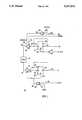
- the FIGUREis a block diagram of an input/output logic module according to a presently preferred embodiment of the invention.
- module 10communicates with input/output pad 12, through which all signals pass to and from the integrated circuit which contains input/output module 10.
- the input portion of input/output module 12includes input buffer 14, having input 16, output 18 and enable input 20.
- Enable input 20 of input buffer 14allows the output of input buffer 14 to be placed in a high impedance state, as is well known in the art.
- Input buffer 14may be a level shifting buffer for translating logic levels between a logic family which is used to drive input/output pad 12 and the logic family used in input/output module 10, which is CMOS in a presently preferred embodiment.
- Output 18 of input buffer 14is connected to a first data input 22 of input two-input multiplexer 24.
- Input two-input multiplexer 24has a second data input 26, which is connected to its output 28, and a select input 30.
- Select input 30 of input two-input multiplexer 24is connected to enable input 20 of input buffer 14, which may be a level shifting buffer as is well known in the art.
- Output 28 of input two-input multiplexer 24is connected to an output node 32, which may be an internal bus of the integrated circuit of which input/output logic module 10 is a part.
- input two-input multiplexer 24is configured as a latch which, in a first state when the logic level at select input 30 is low, acts as a pass through device, and, in a second state, when select input is high, acts as a latch by feeding back output 28 through input 26.
- Select input 30 of input two-input multiplexer 24 and enable input 20 of input buffer 14are driven from output 34 of gate 36, shown as an OR gate with a non-inverted input 38 driven by a signal GIN and an inverted input 40 driven by a signal INEN.
- the output section of input/output logic module 10 of the present inventionincludes an output two-input multiplexer 42, having a first data input 44, connected to an internal bus 46 in the integrated circuit which contains input/output logic module 10.
- a second data input 48 of output two-input multiplexer 42is connected to its output 50.
- output two-input multiplexer 42is configured as a latch which acts as a pass-through when the logic level on select input 52 is low and as a latch when the logic input on select input 52 is high.
- the output 50 of output two-input multiplexer 42is connected to the input 54 of output buffer 56.
- the output 58 of output buffer 56is connected to input/output pad 12.
- Output buffer 56has an enable input 60 which may be used, as is well known in the art, to place output 58 of output buffer 56 in a high impedance state so that input/output pad 12 may drive input buffer 14 without bus contention.
- Enable input 60 of output buffer 56is driven by output 62 of gate 64.
- gate 64is an AND gate having inputs 66 and 68. Input 66 is driven by a signal OUTEN and input 68 is driven by a signal EN.
- the two-input multiplexers and other logic elements disclosed hereinmay be fabricated using conventional MOS and CMOS technology.
- output buffer 56also has a slew input 70, which allows selection of a fast or slow slew rate for the signal at the output 58 of output buffer 56.
- Circuits for slew rate adjustmentare well known in the art.
- the slew rate circuitshould be designed so as to set the fast rate at about 0.6 volts/nanosecond fall time and to set the slow slew rate at about 0.3 volts/nanosecond for driving a 50 pF load.
- the input and output sections of the input/output logic module of the present inventionmay be controlled so as to allow flexibility for the user.
- the slew ratemay be set by tying the slew rate input select line to V DD or to ground. Connecting the GIN input to V DD disables the input buffer, assuming that the INEN input is connected to ground. Connecting the. EN input to ground disables the input buffer, assuming that the OUTEN input is held at V DD . Tying the GIN and EN inputs together to an internal driver or other I/O pad results in a an I/O control allowing the pad 12 to be selectively used for both input and output functions. Output enable signal OUTEN and input enable signal INEN may be used for controlling the input or output function for other purposes, such as testing.
Landscapes
- Engineering & Computer Science (AREA)
- Computer Hardware Design (AREA)
- Physics & Mathematics (AREA)
- Computing Systems (AREA)
- General Engineering & Computer Science (AREA)
- Mathematical Physics (AREA)
- Logic Circuits (AREA)
- Dram (AREA)
Abstract
Description
1. Field of the Invention
The present invention relates to digital electronic circuits. More specifically, the present invention relates to circuits for providing input/output interface functions in integrated circuits, and particularly for providing input/output interface functions in
user-configurable integrated circuits.
2. The Prior Art
Circuits are known in the prior art for providing input/output interface functions in integrated circuits. Examples of such circuits include the circuits disclosed and claimed in U.S. Pat. No. 4,717,912 to Harvey et al. In addition, the X3000 family of programmable devices manufactured by Xilinx are known to have registered or direct outputs and slew rate control.
An input/output module circuit for providing input/output interface functions in integrated circuits includes an input section and an output section electrically connected to an I/O pad of the integrated circuit. The input section includes an input buffer/level shifter for translating the logic signals from the outside world to CMOS compatible levels. The input buffer may be placed in a high impedance state by a control signal applied to a control input. The output of the input buffer/level shifter is connected to a first data input of a two-input multiplexer. The output of the two-input multiplexer is connected to an internal bus and to the second data input of the two-input multiplexer. The select input of the two-input multiplexer is connected to a control signal, preferably to the same control signal used to enable the input buffer/level shifter. This interconnection allows the two-input multiplexer to be used as a data latch. When the select input is low, the output follows the input (the first data input) and when the select input is high, the output state is fed back through the second data input and is thus latched. The control signal may be derived from logical combination of other signals.
The output section of the input/output module section of the present invention includes a two-input multiplexer having a first input connected to an internal data bus, and its output fed back to its second data input. Its select input is driven from a control signal. The output of the two-input multiplexer is also connected to the input of an HCT buffer. The output of the HCT buffer is connected to an I/O pad of the integrated circuit, which may be the same pad to which the input section is connected.
The slew input of the HCT buffer is driven from a signal enabling slow or fast rise times. The enable input of the HCT buffer is driven from an enable signal which may be derived from other logic signals.
The FIGURE is a block diagram of an input/output logic module according to a presently preferred embodiment of the invention.
Referring to the FIGURE, a presently preferred input/output module 10 according to the present invention, it can be seen thatmodule 10 communicates with input/output pad 12, through which all signals pass to and from the integrated circuit which contains input/output module 10.
The input portion of input/output module 12 includesinput buffer 14, havinginput 16,output 18 and enableinput 20. Enableinput 20 ofinput buffer 14 allows the output ofinput buffer 14 to be placed in a high impedance state, as is well known in the art.Input buffer 14 may be a level shifting buffer for translating logic levels between a logic family which is used to drive input/output pad 12 and the logic family used in input/output module 10, which is CMOS in a presently preferred embodiment.
As will be apparent to those of ordinary skill in the art, input two-input multiplexer 24 is configured as a latch which, in a first state when the logic level atselect input 30 is low, acts as a pass through device, and, in a second state, when select input is high, acts as a latch by feeding backoutput 28 throughinput 26.
Selectinput 30 of input two-input multiplexer 24 and enableinput 20 ofinput buffer 14 are driven fromoutput 34 ofgate 36, shown as an OR gate with a non-invertedinput 38 driven by a signal GIN and an invertedinput 40 driven by a signal INEN.
The output section of input/output logic module 10 of the present invention includes an output two-input multiplexer 42, having afirst data input 44, connected to an internal bus 46 in the integrated circuit which contains input/output logic module 10. Asecond data input 48 of output two-input multiplexer 42 is connected to itsoutput 50. Those of ordinary skill in the art will realize that, like input two-input multiplexer 24, output two-input multiplexer 42 is configured as a latch which acts as a pass-through when the logic level onselect input 52 is low and as a latch when the logic input onselect input 52 is high.
Theoutput 50 of output two-input multiplexer 42 is connected to theinput 54 ofoutput buffer 56. Theoutput 58 ofoutput buffer 56 is connected to input/output pad 12.Output buffer 56 has an enableinput 60 which may be used, as is well known in the art, to placeoutput 58 ofoutput buffer 56 in a high impedance state so that input/output pad 12 may driveinput buffer 14 without bus contention.Enable input 60 ofoutput buffer 56 is driven byoutput 62 ofgate 64. In a presently preferred embodiment,gate 64 is an ANDgate having inputs Input 66 is driven by a signal OUTEN andinput 68 is driven by a signal EN.
The two-input multiplexers and other logic elements disclosed herein may be fabricated using conventional MOS and CMOS technology.
In a presently preferred embodiment,output buffer 56 also has aslew input 70, which allows selection of a fast or slow slew rate for the signal at theoutput 58 ofoutput buffer 56. Circuits for slew rate adjustment are well known in the art. In a presently preferred embodiment, the slew rate circuit should be designed so as to set the fast rate at about 0.6 volts/nanosecond fall time and to set the slow slew rate at about 0.3 volts/nanosecond for driving a 50 pF load.
The input and output sections of the input/output logic module of the present invention may be controlled so as to allow flexibility for the user. The slew rate may be set by tying the slew rate input select line to VDD or to ground. Connecting the GIN input to VDD disables the input buffer, assuming that the INEN input is connected to ground. Connecting the. EN input to ground disables the input buffer, assuming that the OUTEN input is held at VDD. Tying the GIN and EN inputs together to an internal driver or other I/O pad results in a an I/O control allowing thepad 12 to be selectively used for both input and output functions. Output enable signal OUTEN and input enable signal INEN may be used for controlling the input or output function for other purposes, such as testing.
While presently-preferred embodiments of the present invention have been disclosed herein, those of ordinary skill in the art will be enabled, from the within disclosure, to configure embodiments which although not expressly disclosed herein nevertheless fall within the scope of the present invention. It is therefore, the intent of the inventors that the scope of the present invention be limited only by the appended claims.
Claims (3)
1. An input/output logic module for use in an integrated circuit, including:
an input/output node for said integrated circuit,
an input buffer having an input connected to said input/output node, an enable input, and an output, said input buffer responsive to a signal on said enable input for placing said output in a high impedance state,
an input two-input multiplexer having a first data input connected to the output of said input buffer, a second data input, a select input, and an output, said output connected to said second data input and to a first internal bus of said integrated circuit,
means for driving said enable input from signals from said integrated circuit,
means for driving said select input from signals from said integrated circuit.
2. An input/output logic module for use in an integrated circuit, including:
an input/output node for said integrated circuit,
an output two-input multiplexer having a first data input connected to a second internal bus of said integrated circuit, a second data input, a select input, and an output, said output connected to said second data input,
an output buffer having an input connected to said output of said output two-input multiplexer, an output connected to said input/output node, and an enable input,
means for driving said enable input from signals from said integrated circuit,
means for driving said select input from signals from said integrated circuit.
3. An input/output logic module for use in an integrated circuit, including:
an input/output node for said integrated circuit,
an input buffer having an input connected to said input/output node, an input buffer enable input, and an output, said input buffer responsive to a signal on said enable input for placing said output in a high impedance state,
an input two-input multiplexer having a first data input connected to the output of said input buffer, a second data input, a select input, and an output, said output connected to said second data input and to a first internal bus of said integrated circuit,
means for driving said input buffer enable input from signals from said integrated circuit,
means for driving the select input of said input two-input multiplexer from signals from said integrated circuit,
an output two-input multiplexer having a first data input connected to a second internal bus of said integrated circuit, a second data input, a select input, and an output, said output connected to said second data input,
an output buffer having an input connected to said output of said output two-input multiplexer, an output connected to said input/output node, and an output buffer enable input,
means for driving said output buffer enable input from signals from said integrated circuit,
means for driving said select input of said output two-input multiplexer from signals from said integrated circuit.
Priority Applications (3)
| Application Number | Priority Date | Filing Date | Title |
|---|---|---|---|
| US07/522,389US5017813A (en) | 1990-05-11 | 1990-05-11 | Input/output module with latches |
| EP19910303917EP0456400A3 (en) | 1990-05-11 | 1991-04-30 | Input/output module with latches |
| JP3131975AJPH04229317A (en) | 1990-05-11 | 1991-05-08 | Input/output logic module used in integrated circuit |
Applications Claiming Priority (1)
| Application Number | Priority Date | Filing Date | Title |
|---|---|---|---|
| US07/522,389US5017813A (en) | 1990-05-11 | 1990-05-11 | Input/output module with latches |
Publications (1)
| Publication Number | Publication Date |
|---|---|
| US5017813Atrue US5017813A (en) | 1991-05-21 |
Family
ID=24080668
Family Applications (1)
| Application Number | Title | Priority Date | Filing Date |
|---|---|---|---|
| US07/522,389Expired - LifetimeUS5017813A (en) | 1990-05-11 | 1990-05-11 | Input/output module with latches |
Country Status (3)
| Country | Link |
|---|---|
| US (1) | US5017813A (en) |
| EP (1) | EP0456400A3 (en) |
| JP (1) | JPH04229317A (en) |
Cited By (44)
| Publication number | Priority date | Publication date | Assignee | Title |
|---|---|---|---|---|
| US5115149A (en)* | 1991-01-24 | 1992-05-19 | Sharp Kabushiki Kaisha | Bidirectional I/O signal separation circuit |
| US5124589A (en)* | 1990-06-19 | 1992-06-23 | Mitsubishi Denki Kabushiki Kaisha | Semiconductor integrated circuit capable of synchronous and asynchronous operations and operating method therefor |
| US5173619A (en)* | 1988-05-26 | 1992-12-22 | International Business Machines Corporation | Bidirectional buffer with latch and parity capability |
| US5243274A (en)* | 1992-08-07 | 1993-09-07 | Westinghouse Electric Corp. | Asic tester |
| US5266847A (en)* | 1990-12-28 | 1993-11-30 | National Semiconductor Corporation | High speed data transceiver |
| GB2269285A (en)* | 1992-07-27 | 1994-02-02 | Siemens Ag | Programmable logic circuit arrangement |
| US5291080A (en)* | 1991-12-27 | 1994-03-01 | Nec Corporation | Integrated circuit device having tristate input buffer for reducing internal power use |
| US5317210A (en)* | 1993-02-23 | 1994-05-31 | Altera Corporation | I/O cell for programmable logic device providing latched, unlatched, and fast inputs |
| US5317211A (en)* | 1993-03-05 | 1994-05-31 | Motorola, Inc. | Programmable pin for use in programmable logic devices |
| US5331220A (en)* | 1993-02-12 | 1994-07-19 | Xilinx, Inc. | Soft wakeup output buffer |
| US5424655A (en)* | 1994-05-20 | 1995-06-13 | Quicklogic Corporation | Programmable application specific integrated circuit employing antifuses and methods therefor |
| US5438282A (en)* | 1993-06-08 | 1995-08-01 | National Semiconductor Corporation | CMOS BTL compatible bus and transmission line driver |
| US5463331A (en)* | 1993-06-08 | 1995-10-31 | National Semiconductor Corporation | Programmable slew rate CMOS buffer and transmission line driver with temperature compensation |
| US5483184A (en)* | 1993-06-08 | 1996-01-09 | National Semiconductor Corporation | Programmable CMOS bus and transmission line receiver |
| US5498976A (en)* | 1990-10-26 | 1996-03-12 | Acer Incorporated | Parallel buffer/driver configuration between data sending terminal and data receiving terminal |
| US5500611A (en)* | 1994-09-30 | 1996-03-19 | Cirrus Logic, Inc. | Integrated circuit with input/output pad having pullup or pulldown |
| US5504440A (en)* | 1994-01-27 | 1996-04-02 | Dyna Logic Corporation | High speed programmable logic architecture |
| US5527745A (en) | 1991-03-20 | 1996-06-18 | Crosspoint Solutions, Inc. | Method of fabricating antifuses in an integrated circuit device and resulting structure |
| US5530386A (en)* | 1993-11-24 | 1996-06-25 | National Semiconductor Corporation | Storage charge reduction circuit for bipolar input/output devices |
| US5539341A (en)* | 1993-06-08 | 1996-07-23 | National Semiconductor Corporation | CMOS bus and transmission line driver having programmable edge rate control |
| US5543746A (en)* | 1993-06-08 | 1996-08-06 | National Semiconductor Corp. | Programmable CMOS current source having positive temperature coefficient |
| US5557223A (en)* | 1993-06-08 | 1996-09-17 | National Semiconductor Corporation | CMOS bus and transmission line driver having compensated edge rate control |
| US5614844A (en)* | 1994-01-27 | 1997-03-25 | Dyna Logic Corporation | High speed programmable logic architecture |
| US5742179A (en)* | 1994-01-27 | 1998-04-21 | Dyna Logic Corporation | High speed programmable logic architecture |
| US5818260A (en)* | 1996-04-24 | 1998-10-06 | National Semiconductor Corporation | Transmission line driver having controllable rise and fall times with variable output low and minimal on/off delay |
| US5869979A (en)* | 1996-04-05 | 1999-02-09 | Altera Corporation | Technique for preconditioning I/Os during reconfiguration |
| US6002268A (en)* | 1993-01-08 | 1999-12-14 | Dynachip Corporation | FPGA with conductors segmented by active repeaters |
| US6005412A (en)* | 1998-04-08 | 1999-12-21 | S3 Incorporated | AGP/DDR interfaces for full swing and reduced swing (SSTL) signals on an integrated circuit chip |
| US6020757A (en)* | 1998-03-24 | 2000-02-01 | Xilinx, Inc. | Slew rate selection circuit for a programmable device |
| US6092226A (en)* | 1998-02-10 | 2000-07-18 | Cray Research, Inc. | Fabrication of test logic for level sensitive scan on a circuit |
| US6107838A (en)* | 1995-02-01 | 2000-08-22 | Honeywell International, Inc. | Simultaneous two-way communication system using a single communication port |
| US6130550A (en)* | 1993-01-08 | 2000-10-10 | Dynalogic | Scaleable padframe interface circuit for FPGA yielding improved routability and faster chip layout |
| US6157204A (en)* | 1998-08-05 | 2000-12-05 | Micron Technology, Inc. | Buffer with adjustable slew rate and a method of providing an adjustable slew rate |
| US6366126B1 (en)* | 1998-12-11 | 2002-04-02 | Nec Corporation | Input circuit, output circuit, and input/output circuit and signal transmission system using the same input/output circuit |
| US20030160632A1 (en)* | 1998-12-31 | 2003-08-28 | Actel Corporation | Programmable multi-standard I/O architecture for FPGAs |
| US6693785B1 (en)* | 1999-12-14 | 2004-02-17 | Koninklijke Philips Electronics N.V. | Electronic component with reduced inductive coupling |
| US6727726B1 (en) | 2002-11-12 | 2004-04-27 | Actel Corporation | Field programmable gate array architecture including a buffer module and a method of distributing buffer modules in a field programmable gate array |
| US20050146354A1 (en)* | 2002-12-18 | 2005-07-07 | Actel Corporation | Multi-level routing architecture in a field programmable gate array having transmitters and receivers |
| US6998884B2 (en) | 2003-12-31 | 2006-02-14 | Atmel Corporation | Circuit for auto-clamping input pins to a definite voltage during power-up or reset |
| US20070152711A1 (en)* | 2005-12-29 | 2007-07-05 | Mun Weon Ahn | Level shifter output buffer circuit usable as an isolation cell |
| US8103806B1 (en)* | 2008-01-18 | 2012-01-24 | Zoran Corporation | Method and apparatus for utilizing device access idle time for input sensing |
| GB2521708A (en)* | 2013-12-31 | 2015-07-01 | Cambridge Silicon Radio Ltd | Chip pads |
| US11671099B2 (en) | 2021-05-21 | 2023-06-06 | Microchip Technology Inc. | Logic cell for programmable gate array |
| US12223322B2 (en) | 2021-10-07 | 2025-02-11 | Microchip Technology Inc. | Embedded processor supporting fixed-function kernels |
Families Citing this family (2)
| Publication number | Priority date | Publication date | Assignee | Title |
|---|---|---|---|---|
| IES80917B2 (en)* | 1997-12-15 | 1999-06-30 | Tellabs Research Limited | Clocking in electronic circuits |
| CN104242901A (en)* | 2013-11-19 | 2014-12-24 | 深圳市邦彦信息技术有限公司 | Device for achieving input function and output function of single IO port at the same time and implementation method thereof |
Citations (8)
| Publication number | Priority date | Publication date | Assignee | Title |
|---|---|---|---|---|
| US4683384A (en)* | 1985-08-09 | 1987-07-28 | Hitachi, Ltd. | Integrated circuit having input and output drivers cascaded between I/O pads and internal circuitry |
| US4697107A (en)* | 1986-07-24 | 1987-09-29 | National Semiconductor Corporation | Four-state I/O control circuit |
| US4709173A (en)* | 1985-05-17 | 1987-11-24 | Matsushita Electric Industrial Co., Ltd. | Integrated circuit having latch circuit with multiplexer selection function |
| US4717912A (en)* | 1982-10-07 | 1988-01-05 | Advanced Micro Devices, Inc. | Apparatus for producing any one of a plurality of signals at a single output |
| US4745305A (en)* | 1985-09-23 | 1988-05-17 | Ncr Corporation | Common cell I/O interface circuit |
| US4896296A (en)* | 1985-03-04 | 1990-01-23 | Lattice Semiconductor Corporation | Programmable logic device configurable input/output cell |
| US4903223A (en)* | 1988-05-05 | 1990-02-20 | Altera Corporation | Programmable logic device with programmable word line connections |
| US4912345A (en)* | 1988-12-29 | 1990-03-27 | Sgs-Thomson Microelectronics, Inc. | Programmable summing functions for programmable logic devices |
Family Cites Families (2)
| Publication number | Priority date | Publication date | Assignee | Title |
|---|---|---|---|---|
| JPS60169216A (en)* | 1984-02-13 | 1985-09-02 | Fujitsu Ltd | flip-flop circuit |
| US4987319A (en)* | 1988-09-08 | 1991-01-22 | Kawasaki Steel Corporation | Programmable input/output circuit and programmable logic device |
- 1990
- 1990-05-11USUS07/522,389patent/US5017813A/ennot_activeExpired - Lifetime
- 1991
- 1991-04-30EPEP19910303917patent/EP0456400A3/ennot_activeCeased
- 1991-05-08JPJP3131975Apatent/JPH04229317A/enactivePending
Patent Citations (8)
| Publication number | Priority date | Publication date | Assignee | Title |
|---|---|---|---|---|
| US4717912A (en)* | 1982-10-07 | 1988-01-05 | Advanced Micro Devices, Inc. | Apparatus for producing any one of a plurality of signals at a single output |
| US4896296A (en)* | 1985-03-04 | 1990-01-23 | Lattice Semiconductor Corporation | Programmable logic device configurable input/output cell |
| US4709173A (en)* | 1985-05-17 | 1987-11-24 | Matsushita Electric Industrial Co., Ltd. | Integrated circuit having latch circuit with multiplexer selection function |
| US4683384A (en)* | 1985-08-09 | 1987-07-28 | Hitachi, Ltd. | Integrated circuit having input and output drivers cascaded between I/O pads and internal circuitry |
| US4745305A (en)* | 1985-09-23 | 1988-05-17 | Ncr Corporation | Common cell I/O interface circuit |
| US4697107A (en)* | 1986-07-24 | 1987-09-29 | National Semiconductor Corporation | Four-state I/O control circuit |
| US4903223A (en)* | 1988-05-05 | 1990-02-20 | Altera Corporation | Programmable logic device with programmable word line connections |
| US4912345A (en)* | 1988-12-29 | 1990-03-27 | Sgs-Thomson Microelectronics, Inc. | Programmable summing functions for programmable logic devices |
Cited By (63)
| Publication number | Priority date | Publication date | Assignee | Title |
|---|---|---|---|---|
| US5173619A (en)* | 1988-05-26 | 1992-12-22 | International Business Machines Corporation | Bidirectional buffer with latch and parity capability |
| US5124589A (en)* | 1990-06-19 | 1992-06-23 | Mitsubishi Denki Kabushiki Kaisha | Semiconductor integrated circuit capable of synchronous and asynchronous operations and operating method therefor |
| US5498976A (en)* | 1990-10-26 | 1996-03-12 | Acer Incorporated | Parallel buffer/driver configuration between data sending terminal and data receiving terminal |
| US5266847A (en)* | 1990-12-28 | 1993-11-30 | National Semiconductor Corporation | High speed data transceiver |
| US5115149A (en)* | 1991-01-24 | 1992-05-19 | Sharp Kabushiki Kaisha | Bidirectional I/O signal separation circuit |
| US5527745A (en) | 1991-03-20 | 1996-06-18 | Crosspoint Solutions, Inc. | Method of fabricating antifuses in an integrated circuit device and resulting structure |
| US5291080A (en)* | 1991-12-27 | 1994-03-01 | Nec Corporation | Integrated circuit device having tristate input buffer for reducing internal power use |
| GB2269285B (en)* | 1992-07-27 | 1995-12-20 | Siemens Ag | Configurable logic cell |
| GB2269285A (en)* | 1992-07-27 | 1994-02-02 | Siemens Ag | Programmable logic circuit arrangement |
| US5243274A (en)* | 1992-08-07 | 1993-09-07 | Westinghouse Electric Corp. | Asic tester |
| US6130550A (en)* | 1993-01-08 | 2000-10-10 | Dynalogic | Scaleable padframe interface circuit for FPGA yielding improved routability and faster chip layout |
| US6002268A (en)* | 1993-01-08 | 1999-12-14 | Dynachip Corporation | FPGA with conductors segmented by active repeaters |
| US5489858A (en)* | 1993-02-12 | 1996-02-06 | Xilinx, Inc. | Soft wakeup output buffer |
| US5331220A (en)* | 1993-02-12 | 1994-07-19 | Xilinx, Inc. | Soft wakeup output buffer |
| US5317210A (en)* | 1993-02-23 | 1994-05-31 | Altera Corporation | I/O cell for programmable logic device providing latched, unlatched, and fast inputs |
| US5317211A (en)* | 1993-03-05 | 1994-05-31 | Motorola, Inc. | Programmable pin for use in programmable logic devices |
| US5438282A (en)* | 1993-06-08 | 1995-08-01 | National Semiconductor Corporation | CMOS BTL compatible bus and transmission line driver |
| US5463331A (en)* | 1993-06-08 | 1995-10-31 | National Semiconductor Corporation | Programmable slew rate CMOS buffer and transmission line driver with temperature compensation |
| US5543746A (en)* | 1993-06-08 | 1996-08-06 | National Semiconductor Corp. | Programmable CMOS current source having positive temperature coefficient |
| US5483184A (en)* | 1993-06-08 | 1996-01-09 | National Semiconductor Corporation | Programmable CMOS bus and transmission line receiver |
| US5557223A (en)* | 1993-06-08 | 1996-09-17 | National Semiconductor Corporation | CMOS bus and transmission line driver having compensated edge rate control |
| US5539341A (en)* | 1993-06-08 | 1996-07-23 | National Semiconductor Corporation | CMOS bus and transmission line driver having programmable edge rate control |
| US5530386A (en)* | 1993-11-24 | 1996-06-25 | National Semiconductor Corporation | Storage charge reduction circuit for bipolar input/output devices |
| US5808479A (en)* | 1994-01-27 | 1998-09-15 | Dyna Logic Corporation | High speed programmable logic architecture |
| US5614844A (en)* | 1994-01-27 | 1997-03-25 | Dyna Logic Corporation | High speed programmable logic architecture |
| WO1997037431A1 (en)* | 1994-01-27 | 1997-10-09 | Dyna Logic Corporation | High speed programmable logic architecture |
| US5742179A (en)* | 1994-01-27 | 1998-04-21 | Dyna Logic Corporation | High speed programmable logic architecture |
| US6218856B1 (en) | 1994-01-27 | 2001-04-17 | Xilinx, Inc. | High speed programmable logic architecture |
| US5504440A (en)* | 1994-01-27 | 1996-04-02 | Dyna Logic Corporation | High speed programmable logic architecture |
| US5654649A (en)* | 1994-05-20 | 1997-08-05 | Quicklogic Corporation | Programmable application specific integrated circuit employing antifuses and methods therefor |
| US5682106A (en)* | 1994-05-20 | 1997-10-28 | Quicklogic Corporation | Logic module for field programmable gate array |
| US5892684A (en)* | 1994-05-20 | 1999-04-06 | Quicklogic Corporation | Programmable application specific integrated circuit employing antifuses and methods therefor |
| US5477167A (en)* | 1994-05-20 | 1995-12-19 | Quicklogic Corporation | Programmable application specific integrated circuit using logic circuits to program antifuses therein |
| US5424655A (en)* | 1994-05-20 | 1995-06-13 | Quicklogic Corporation | Programmable application specific integrated circuit employing antifuses and methods therefor |
| US5500611A (en)* | 1994-09-30 | 1996-03-19 | Cirrus Logic, Inc. | Integrated circuit with input/output pad having pullup or pulldown |
| US6107838A (en)* | 1995-02-01 | 2000-08-22 | Honeywell International, Inc. | Simultaneous two-way communication system using a single communication port |
| US6208162B1 (en) | 1996-04-05 | 2001-03-27 | Altera Corporation | Technique for preconditioning I/Os during reconfiguration |
| US5869979A (en)* | 1996-04-05 | 1999-02-09 | Altera Corporation | Technique for preconditioning I/Os during reconfiguration |
| US5818260A (en)* | 1996-04-24 | 1998-10-06 | National Semiconductor Corporation | Transmission line driver having controllable rise and fall times with variable output low and minimal on/off delay |
| US6092226A (en)* | 1998-02-10 | 2000-07-18 | Cray Research, Inc. | Fabrication of test logic for level sensitive scan on a circuit |
| US6020757A (en)* | 1998-03-24 | 2000-02-01 | Xilinx, Inc. | Slew rate selection circuit for a programmable device |
| US6184708B1 (en)* | 1998-03-24 | 2001-02-06 | Xilinx, Inc. | Method for selecting slew rate for a programmable device |
| US6005412A (en)* | 1998-04-08 | 1999-12-21 | S3 Incorporated | AGP/DDR interfaces for full swing and reduced swing (SSTL) signals on an integrated circuit chip |
| US6157204A (en)* | 1998-08-05 | 2000-12-05 | Micron Technology, Inc. | Buffer with adjustable slew rate and a method of providing an adjustable slew rate |
| US6300788B1 (en) | 1998-08-05 | 2001-10-09 | Micron Technology, Inc. | Buffer with adjustable slew rate and a method of providing an adjustable slew rate |
| US6504396B2 (en) | 1998-08-05 | 2003-01-07 | Micron Technology, Inc. | Method for adjusting an output slew rate of a buffer |
| US6366126B1 (en)* | 1998-12-11 | 2002-04-02 | Nec Corporation | Input circuit, output circuit, and input/output circuit and signal transmission system using the same input/output circuit |
| US20030160632A1 (en)* | 1998-12-31 | 2003-08-28 | Actel Corporation | Programmable multi-standard I/O architecture for FPGAs |
| US6617875B2 (en) | 1998-12-31 | 2003-09-09 | Actel Corporation | Programmable multi-standard I/O architecture for FPGAs |
| US6762621B1 (en) | 1998-12-31 | 2004-07-13 | Actel Corporation | Programmable multi-standard I/O architecture for FPGAs |
| US6909306B2 (en) | 1998-12-31 | 2005-06-21 | Actel Corporation | Programmable multi-standard I/O architecture for FPGAS |
| US6693785B1 (en)* | 1999-12-14 | 2004-02-17 | Koninklijke Philips Electronics N.V. | Electronic component with reduced inductive coupling |
| US6727726B1 (en) | 2002-11-12 | 2004-04-27 | Actel Corporation | Field programmable gate array architecture including a buffer module and a method of distributing buffer modules in a field programmable gate array |
| US20050146354A1 (en)* | 2002-12-18 | 2005-07-07 | Actel Corporation | Multi-level routing architecture in a field programmable gate array having transmitters and receivers |
| US7126374B2 (en) | 2002-12-18 | 2006-10-24 | Actel Corporation | Multi-level routing architecture in a field programmable gate array having transmitters and receivers |
| US6998884B2 (en) | 2003-12-31 | 2006-02-14 | Atmel Corporation | Circuit for auto-clamping input pins to a definite voltage during power-up or reset |
| US20070152711A1 (en)* | 2005-12-29 | 2007-07-05 | Mun Weon Ahn | Level shifter output buffer circuit usable as an isolation cell |
| US8103806B1 (en)* | 2008-01-18 | 2012-01-24 | Zoran Corporation | Method and apparatus for utilizing device access idle time for input sensing |
| GB2521708A (en)* | 2013-12-31 | 2015-07-01 | Cambridge Silicon Radio Ltd | Chip pads |
| US9331673B2 (en) | 2013-12-31 | 2016-05-03 | Qualcomm Technologies International, Ltd. | Integrated circuit operating active circuitry and chip pads in different operating modes and at different voltage levels |
| GB2521708B (en)* | 2013-12-31 | 2021-05-05 | Qualcomm Technologies Int Ltd | Chip pads |
| US11671099B2 (en) | 2021-05-21 | 2023-06-06 | Microchip Technology Inc. | Logic cell for programmable gate array |
| US12223322B2 (en) | 2021-10-07 | 2025-02-11 | Microchip Technology Inc. | Embedded processor supporting fixed-function kernels |
Also Published As
| Publication number | Publication date |
|---|---|
| EP0456400A3 (en) | 1992-04-15 |
| EP0456400A2 (en) | 1991-11-13 |
| JPH04229317A (en) | 1992-08-18 |
Similar Documents
| Publication | Publication Date | Title |
|---|---|---|
| US5017813A (en) | Input/output module with latches | |
| US4987319A (en) | Programmable input/output circuit and programmable logic device | |
| US5602494A (en) | Bi-directional programmable I/O cell | |
| US5568062A (en) | Low noise tri-state output buffer | |
| US6472904B2 (en) | Double data rate input and output in a programmable logic device | |
| US5563532A (en) | Double filtering glitch eater for elimination of noise from signals on a SCSI bus | |
| US5280203A (en) | Look-ahead asynchronous register set/reset in programmable logic device | |
| KR100591520B1 (en) | Tri-state buffer with reduced voltage input and output and its manufacturing method | |
| JPH05291940A (en) | Gradually turning on cmos driver | |
| GB2239997A (en) | Output driver | |
| US6239612B1 (en) | Programmable I/O cells with multiple drivers | |
| US5315174A (en) | Programmable output slew rate control | |
| US6118324A (en) | Output driver with reduced ground bounce | |
| US5600266A (en) | Digital logic output buffer interface for different semiconductor technologies | |
| US7417454B1 (en) | Low-swing interconnections for field programmable gate arrays | |
| CA2468928C (en) | High-speed output circuit with low voltage capability | |
| US6163169A (en) | CMOS tri-state control circuit for a bidirectional I/O with slew rate control | |
| US7474124B2 (en) | Electronic circuit for maintaining and controlling data bus state | |
| US5508640A (en) | Dynamic CMOS logic circuit with precharge | |
| JP2772051B2 (en) | Programmable input / output circuit and programmable logic element | |
| US5952850A (en) | Input/output circuit and a method for controlling an input/output signal | |
| KR20000017051A (en) | Transceiver driver with programmable edge rate control independent of fabrication process, supply voltage, and temperature | |
| US6175598B1 (en) | Output noise control scheme for multiple I/O's | |
| US5329181A (en) | Complementary macrocell feedback circuit | |
| US6154059A (en) | High performance output buffer |
Legal Events
| Date | Code | Title | Description |
|---|---|---|---|
| AS | Assignment | Owner name:ACTEL CORPORATION, A CORP. OF CA., CALIFORNIA Free format text:ASSIGNMENT OF ASSIGNORS INTEREST.;ASSIGNORS:GALBRAITH, DOUGLAS C.;GREENE, JONATHAN W.;REEL/FRAME:005332/0055 Effective date:19900510 | |
| STCF | Information on status: patent grant | Free format text:PATENTED CASE | |
| FPAY | Fee payment | Year of fee payment:4 | |
| FEPP | Fee payment procedure | Free format text:PAYOR NUMBER ASSIGNED (ORIGINAL EVENT CODE: ASPN); ENTITY STATUS OF PATENT OWNER: LARGE ENTITY | |
| FPAY | Fee payment | Year of fee payment:8 | |
| FPAY | Fee payment | Year of fee payment:12 |