US5012153A - Split collector vacuum field effect transistor - Google Patents
Split collector vacuum field effect transistorDownload PDFInfo
- Publication number
- US5012153A US5012153AUS07/455,217US45521789AUS5012153AUS 5012153 AUS5012153 AUS 5012153AUS 45521789 AUS45521789 AUS 45521789AUS 5012153 AUS5012153 AUS 5012153A
- Authority
- US
- United States
- Prior art keywords
- collector
- conductive
- steering
- fet
- vacuum
- Prior art date
- Legal status (The legal status is an assumption and is not a legal conclusion. Google has not performed a legal analysis and makes no representation as to the accuracy of the status listed.)
- Expired - Lifetime
Links
Images


Classifications
- H—ELECTRICITY
- H01—ELECTRIC ELEMENTS
- H01J—ELECTRIC DISCHARGE TUBES OR DISCHARGE LAMPS
- H01J21/00—Vacuum tubes
- H01J21/02—Tubes with a single discharge path
- H01J21/06—Tubes with a single discharge path having electrostatic control means only
- H01J21/10—Tubes with a single discharge path having electrostatic control means only with one or more immovable internal control electrodes, e.g. triode, pentode, octode
- H01J21/105—Tubes with a single discharge path having electrostatic control means only with one or more immovable internal control electrodes, e.g. triode, pentode, octode with microengineered cathode and control electrodes, e.g. Spindt-type
- H—ELECTRICITY
- H01—ELECTRIC ELEMENTS
- H01J—ELECTRIC DISCHARGE TUBES OR DISCHARGE LAMPS
- H01J3/00—Details of electron-optical or ion-optical arrangements or of ion traps common to two or more basic types of discharge tubes or lamps
- H01J3/02—Electron guns
- H01J3/021—Electron guns using a field emission, photo emission, or secondary emission electron source
- H01J3/022—Electron guns using a field emission, photo emission, or secondary emission electron source with microengineered cathode, e.g. Spindt-type
- H—ELECTRICITY
- H03—ELECTRONIC CIRCUITRY
- H03K—PULSE TECHNIQUE
- H03K17/00—Electronic switching or gating, i.e. not by contact-making and –breaking
- H03K17/51—Electronic switching or gating, i.e. not by contact-making and –breaking characterised by the components used
- H03K17/54—Electronic switching or gating, i.e. not by contact-making and –breaking characterised by the components used by the use, as active elements of vacuum tubes
- H03K17/545—Electronic switching or gating, i.e. not by contact-making and –breaking characterised by the components used by the use, as active elements of vacuum tubes using microengineered devices, e.g. field emission devices
Definitions
- This inventiondeals with an improvement to vacuum field effect transistors (FETs) having field emission cathode structures, and with circuits employing these devices.
- FETsvacuum field effect transistors
- the first vacuum FET(also called a microelectronic tube) was announced in 1986 by Dr. Henry Gray of the Naval Research Laboratory. The announcement generated a considerable amount of interest, and stimulated further developments in the technology on an international scale.
- the vacuum FETis basically an electron tube fabricated on a microelectronic scale using semiconductor processing techniques. Due to extremely small dimensions of the device (cathode tip to anode spacings are typically 0.5 micrometer), the mean free path of the electrons can be greater than the cathode tip to anode spacing, allowing vacuum tube type operation at pressures up to 1/100 to 1 atmosphere.
- the vacuum FEThas distinct advantages over other semiconductor devices in terms of radiation hardness, extreme temperature insensitivity, very high speed operation and power efficiency, small and light weight packages, and relatively low cost. The development of the technology is reviewed in an article by Kathy Skidmore, "The Comeback of the Vacuum Tube: Will Semiconductor Versions Supplement Transistors?", Semiconductor International, August 1988, pages 15-18. The basic structure is described in U.S. Pat. No. 4,721,885 to Brodie.
- the structure of the current vacuum FETis shown in FIG. 1.
- the deviceis formed on a substrate 2, which may be ceramic, glass, metal or silicon.
- a conductive layer 4is deposited over the substrate.
- the electron emitter 6may be formed either from silicon, or from a refractory metal such as molybdenum or tungsten.
- An insulating dielectric layer 8such as silicon dioxide is then deposited over the conductive layer 4, followed by the deposition of a metal film 10 which functions as the gate electrode. Silicon is preferred for the conductive layer 4 because of the ease of growing the oxide 8 with a high dielectric strength over it.
- Dielectric layer 8 and gate electrode 10are etched to form a gap around the periphery of electron emitter 6, with the tip of the electron emitter centered in the opening and approximately level with the upper gate electrode surface to maximize the electric field at the tip.
- a second insulating layer 12is then deposited over gate electrode 10 and etched to expose the electron emitter.
- a metal film 14is deposited over dielectric layer 12 to form the anode or collector.
- the collector 14covers an interior chamber 16 within the device, which is maintained at a partial vacuum generally within the range of 0.01 to 1 atmosphere.
- a collector voltage V Cis applied to collector plate 14 to extract an electron stream from emitter 6.
- the gate electrode 10is biased by a gate control voltage V G to modulate the emitted current in an amplifier mode, or to switch the current emission on and off completely in a logic switching mode.
- the standard device of FIG. 1merely provides a basic amplifying or switching element. As with standard semiconductor transistors, a number of such devices must be connected together to perform higher level functions such as multiplexing, frequency multiplication, logical AND or EXCLUSIVE OR. In this sense, the basic vacuum FET provides no new functionality over existing solid state technologies.
- the present inventionextends the capabilities of the vacuum FET by providing for a variety of higher level functions in a single circuit element, thus adding new flexibility to solid state circuits based upon vacuum FETs. Reducing higher level functions into a single device structure also results in circuits that are simpler and more compact.
- the segments of the collectorcan be electrically isolated from each other or connected together in various combinations, depending on the output function desired.
- the electrical isolation of the separate collector segmentsis preferably implemented as one or more gaps through which the current can flow without striking the conductive collector segments.
- An electron sinkis preferably positioned on the opposite side of the collector from the emitter, to capture electrons which pass through a collector gap. The electron sink is biased at or slightly more positive than the collector, allowing the current to pass freely through the gap and be absorbed by the electron sink.
- inventions for the new vacuum FETinclude an AND gate, EXCLUSIVE OR gate, signal demultiplexer and frequency multiplier.
- an AND gateone input signal, applied between the cathode tip and the split collecting anodes, induces current emission from the cathode tip.
- the second inputapplied between the steering gate electrodes, steers the emitted beam to the output of the device.
- the emitted currentpasses straight through the device, passing through a central gap in the collector, and impinging on the electrically isolated electron sink plate so that no output voltage is generated.
- the second input signalis applied there is no emitted current, and again no output signal is generated. Only with the presence of both input signals is the current emission induced and steered to the proper collector segment of the device, generating an output voltage. With either of the inputs missing, the output voltage is zero.
- both inputsare applied to the steering gate electrodes.
- the collector platesare electrically connected and biased positively, to induce a constant emission current from the tip.
- the emitted currentpasses straight through the device, passing through a central gap in the collector, and impinging on the electrically isolated electron sink plate so that no output voltage is generated.
- the emitted currentis steered to one of the collecting plates and generates an output voltage.
- An EXCLUSIVE NOR functioncan be obtained by reversing the conductive and non-conductive portions of the collector.
- the collectoris formed into at least two electrically isolated plates that are separated from each other by isolating gaps. Each separate collector segment is connected to a different output circuit for the device.
- a multiplexed input signalis applied to the steering electrode, and has superimposed upon it a steering signal which alternately steers the emitted current between the separate conductor plates in synchronism with the input signal multiplexing. The input signal is thus demultiplexed among the separate output circuits of the device.
- the collectoris divided into at least three conductive segments which are mutually spaced apart from each other by isolating gaps.
- a sweep signalis applied to the steering electrode to sweep the emitter current across the conductive segments and isolating gaps, with an output produced each time the current strikes a conductive collector segment; the collector segments are preferably connected in common.
- FIG. 1is a sectional view of a prior art vacuum FET
- FIGS. 2 and 3are respectively sectional and fragmentary plan views of a vacuum FET in accordance with the present invention implemented as an AND gate;
- FIGS. 4 and 5are respectively sectional and fragmentary plan views of a vacuum FET in accordance with the invention implemented as an EXCLUSIVE OR gate;
- FIGS. 6 and 7are respectively sectional and fragmentary plan views of a vacuum FET in accordance with the invention implemented as a signal demultiplexer;
- FIG. 8illustrates the input and output signal waveforms for the demultiplexer device of FIGS. 6 and 7;
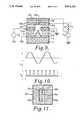
- FIG. 9is a sectional view of a vacuum FET in accordance with the invention implemented as a frequency multiplier
- FIG. 10illustrates the input and output signal waveforms for the signal multiplier of FIG. 9;
- FIG. 11is a plan view of a collector used with the device of FIG. 9;
- FIG. 12is a functional diagram illustrating the electron current steering achieved with the invention.
- FIGS. 13a-13eare sectional views showing successive steps in the fabrication of a vacuum FET in accordance with the invention.
- the present inventionintegrates higher level circuit functions into a single vacuum FET device by dividing the collector into separate, electrically isolated conducting plates, and using the gate electrode as a steering electrode to direct an emitted electron stream onto a desired portion of the collector in accordance with an applied input signal.
- the output taken from the collectorvaries according to where the electron stream hits the collector, thereby allowing the FET to perform circuit functions in addition to the simple switching and amplification of prior vacuum FETs.
- an electron sink behind the collectoris biased at or slightly more positive than the collector plates in order to capture any electrons that pass through a collector gap, thus achieving the nonconductive segments of the divided collector.
- FIG. 2An implementation of the invention as an AND gate is shown in FIG. 2.
- the substrate 2, conductive layer 4 and emitter 6may be the same as in the prior vacuum FET shown in FIG. 1.
- Emitter 6extends upward from the floor of chamber 16, terminating in an electron emitting upper tip 18.
- a dielectric layer 20 such as SiO 2is formed over conductive layer 4.
- a steering electrode means in the form of a pair of individual steering gate electrodes 22a and 22bare positioned over dielectric layer 20 on opposite sides of chamber 16. Unlike the prior vacuum FET in FIG. 1, the steering gate electrodes are electrically isolated from each other so that they can be independently biased. Also unlike the prior vacuum FET of FIG. 1, in which the upper surface of gate electrode 10 is approximately even with the tip of electron emitter 6, in the device of FIG. 2 dielectric layer 20 has a greater vertical dimension so that steering electrodes 22a and 22b are positioned just above the level of electron emitting tip 18. This permits them to effectively steer the electron stream emitted from the tip.
- collector 26is formed over the steering electrodes and surmounted by a collector, generally indicated by reference numeral 26.
- collector 26is divided into two conductive sections 26a and 26b which are positioned on opposite sides of chamber 16. Collector sections 26a and 26b are electrically isolated from each other, and separated by a gap which is vertically aligned with the emitter tip.
- a third dielectric layer 28is provided over the collector and forms a continuation of interior chamber 16 in alignment with the inside walls of second dielectric layer 24.
- Conductive layer 30serves as an electron sink to collect electrons from emitter 6 which flow either to or past the conductive collector sections, as described below.
- a plan view of electron sink 30, collector sections 26a, 26b and their vertical alignment with emitter 6 and steering electrodes 22a, 22bis shown in FIG. 3, in which visible elements are indicated by hatch lines.
- the left-hand steering electrode 22ais held together with conductive layer 4 and emitter 6 at a reference voltage, preferably ground.
- One input electrical signal V 1is applied to the current sink 30 and to collector sections 26a, 26b to induce an electron emission from emitter 6; the connection to collector section 26b is made through a resistor R1.
- a second input signal V 2is connected to the right-hand steering electrode 22b. The output is taken as voltage V 0 across R1.
- the electrostatic potential created by the application of V 1induces electron emission from the emitting tip 6.
- the electric field generated by the application of V 2is such that it steers the emitted beam toward collector plate 22b with a positive voltage.
- both signals V 1 and V 2are applied, current is extracted from the emitting tip and diverted by the V 2 signal on gate electrode 22b to the right-hand collector section 26b.
- the currentflows through resistor R1 from collector section 26b, producing an output voltage V 0 which indicates the presence of both input signals V 1 and V 2 .
- V 1 but not V 2an electron stream is extracted from emitter 6 but flows between the voltage balanced collector sections to be captured by electron sink 30, so that no output voltage V 0 appears across R1.
- V 2 but not V 1no current is extracted from emitter 6 and again there is no output voltage across R1.
- the devicethus functions as an AND gate, producing an output voltage only when both input signals are present.
- the “nonconductive” portion of collector 26comprises the gap between collector sections 26a and 26b together with an electron sink 30 situated behind the gap, biased at the same potential or slightly more positive than the collector plates. While this is the preferred embodiment, the term “nonconductive” can be broadly interpreted to mean nonconductive with respect to the output circuit R1. For example, if the collector gap were filled by a conductive current sink electrically isolated from output circuit R1, the device could still function as an AND gate within the scope of the invention.
- FIGS. 4 and 5show an EXCLUSIVE OR gate using the new vacuum FET structure.
- the collectorconsists of a conductive plate 32 having a central slot 34 which is aligned over emitter 6 and parallel to steering electrodes 22a, 22b.
- Input signal sources V 1 and V 2are connected to the steering electrodes 22a, 22b, respectively.
- a bias voltage source V Cis connected to electron sink 30 and, through resistor R1 to the collector plate 32.
- the conducting collector segmentsare electrically connected in common.
- V Cinduces a constant emission of electrons from emitter 6.
- the electron beampasses through the gap in the collector plate 32 formed by slot 34, and impinges upon electron sink 30.
- the output voltage V O across R1is zero, under these conditions. If one or the other of the inputs V 1 or V 2 is high, the emitted electron beam is steered onto the conductive portion of the collector 32, causing a current to flow through R1, generating a positive output voltage V O . If both input signals V 1 and V 2 are applied to steering electrodes 22a and 22b, the steering voltages balance each other so that the electron beam is again steered directly down the center axis of the device and through the nonconductive slot 34, so that the output V O is again zero.
- a variation on the EXCLUSIVE OR device shown in FIGS. 4 and 5would be to reverse the conductive and nonconductive portions of the collector, so that a conductive plate would occupy the area of slot 34 with the remainder of the collector open.
- FIGS. 6 and 7show another embodiment of the new vacuum FET, implemented as a signal demultiplexer.
- the collectorconsists of two conductive plates 36a, 36b which are spaced apart on opposite sides of the nonconductive gap and are electrically isolated from each other.
- Each collector sectionhas an associated output circuit, resistor R1 for section 36a and resistor R2 for section 36b, with the output circuits supplied by source V C .
- the V C sourcealso applies a bias to the electron sink 30.
- a multiplexed input signal V iis superimposed upon a steering signal V S and applied to steering electrode 22a, with the other steering electrode 22b grounded.
- Steering voltage V Salternates in synchronism with the multiplexing of the input signal V i , thus switching the emitted electron beam between collector plates 36a and 36b in synchronism with the input signal multiplexing.
- Output circuit R1thus obtains one of the multiplexed input signals, and output circuit R2 the other.
- the pertinent signal waveformsare illustrated in FIG. 8.
- the multiplexed input signal V ishifts at time 38 from one input signal pattern to another.
- steering voltage V SPrior to this time, steering voltage V S is negative, causing steering electrode 22a to repel emitted electrons and direct them onto conductive collector section 36b. This results in an output V O1 across output resistor R1, with no output V O2 across output resistor R2.
- V Sgoes positive, deflecting the emitted electron beam off of collector section 36b and onto collector section 36a. This results in an output V O2 across output resistor R2, and no output V O1 across output resistor R1.
- the steering voltage V Scontinues to periodically alternate in synchronism with the multiplexing of input signal V i .
- the input signalis demultiplexed, with one of its constituent components appearing across R1 and the other across R2.
- FIGS. 9-11The application of the invention to a frequency multiplier function is shown in FIGS. 9-11.
- the collectorconsists of at least three conductive sections 40a, 40b, 40c which are spaced apart by nonconductive segments. Although the conductive sections could be isolated from each other and provided with separate output circuits, they are preferably electrically connected in common.
- FIG. 11A simple collector construction for this purpose is shown in FIG. 11, in which the collector consists of a plate 40 having a pair of open parallel slots 42a, 42b.
- the conductive collector sections 40a, 40b and 40cconsist of the plate portions on either side of the slots, and between the slots, respectively.
- the bias voltage V Cis connected to the electron sink 30 and, through resistor R1, to the collector plate 40.
- An alternating input sweep signal V S having a particular frequencyis applied to one of the steering electrodes 22a, with the other steering electrode 22b grounded. Sweep voltage V S steers the electron beam from emitter 6 back and forth across the collector grid. As the beam passes over the grid, at any given time it either impinges upon one of the conductive grid portions 40a, 40b, 40c to cause a current to flow through output resistor R1, or passes through one of the collector slots 42a, 42b to be absorbed by electron sink 30.
- the resulting output waveform V Ois illustrated in FIG. 10. Its frequency is a multiple of the input V S frequency, the multiplication factor depending upon the number of spaced conductive portions provided in the collector grid.
- the operation of the various vacuum FET implementations described abovedepends upon the ability to steer the emitter electron beam.
- the basic steering geometryis illustrated in FIG. 12.
- the angle ⁇ by which the emitter electron beam 44 is deflected as it passes between the steering electrodes 22a, 22bcan be calculated as a function of the steering voltage V S in accordance with the following formula: ##EQU1## where ⁇ w is the work function of the emitting tip 18 and e is the electronic charge.
- ⁇ wis the work function of the emitting tip 18
- eis the electronic charge.
- This relationshipimplies that the geometry of the device can be tailored to provide a given angular deflection for the desired steering voltage V S .
- the exact voltage levels required for V Swill depend upon the work function and radius of the emitting tip, the necessary extraction voltage V C , and the aspect ratios achievable in the fabrication process, which determine the height h of the steering electrodes and the spacing w between them.
- FIGS. 13a-13eOne suitable fabrication process for the new split collector vacuum FET is illustrated in FIGS. 13a-13e.
- the conductive layer 4is grown upon a substrate 2 which is preferably formed from a ceramic, glass, metal or silicon, followed by the growth of oxide layer 20.
- a metal layer 22which will later be formed into the steering electrodes is evaporated onto the oxide layer 20; a refractory metal is preferred because of its high melting point.
- An insulating layer such as Si 3 N 4is then deposited by a suitable process such as chemical vapor deposition over metal layer 22.
- a photoresist layer 44is next applied over insulator layer 24, with an opening left for the formation of chamber 16.
- the chambermay then be formed by a dry etch such as fluoride reactive ion etching for the insulator layer 24 and metal electrode layer 22, followed by a wet chemical etch such as buffered hydrofluoric acid solution for the oxide layer 20.
- a dry etchsuch as fluoride reactive ion etching for the insulator layer 24 and metal electrode layer 22
- a wet chemical etchsuch as buffered hydrofluoric acid solution for the oxide layer 20.
- emitter cone 6is formed by rotating the device during an angled metal evaporation process as described in Spindt et al., "Physical Properties of Thin-Film Field Emission Cathodes With Molybdenum Cathode Cones", Journal of Applied Physics, Vol. 47, No. 12, 1976, pages 5,248-5,263.
- the evaporationalso deposits a layer of metal 46 over photoresist layer 44.
- the photoresistis then dissolved, which also removes the overlying metal layer 46.
- a planarizing polymer 48has been spun over the entire device, including the interior of chamber 16.
- the planarizing polymeris then etched back as with an oxygen plasma process until it is flush with the upper surface of dielectric layer 24, and the collector metal 26 is evaporated on top (FIG. 13d).
- Dielectric layer 28is then formed over the collector layer.
- the desired pattern of collector openingsis next patterned and dry etched through the top dielectric layer 28 down to the collector, followed by patterning and etching away the desired openings from the collector itself.
- the resultis shown in FIG. 13e for the AND gate of FIG. 2.
- the previously applied planarizing polymerextends up to the bottom of the collector; additional polymer is spun on until it is flush with the upper surface of top dielectric layer 28.
- Thisprovides a support for the electron sink 30, which consists of a solid metal plate evaporated over dielectric layer 28 and the planarizing polymer of chamber 16.
- the electron sinkis lithographically patterned and etched as in FIGS. 3, 5 and 7, so as to provide an electrode over the central active area of the device and access ports to the chamber in the outlying area.
- the polymer remaining within chamber 16is dissolved by flowing a suitable solvent into the chamber through the exposed portions of the collector slots on either side of the electron sink 30.
- the solventshould be selected so that it dissolves the planarizing polymer faster than the metal or dielectric layers forming the boundary of the chamber; solutions such as acetone and trichloroethane are suitable for this purpose.
Landscapes
- Cold Cathode And The Manufacture (AREA)
Abstract
Description
1. Field of the Invention
This invention deals with an improvement to vacuum field effect transistors (FETs) having field emission cathode structures, and with circuits employing these devices.
2. Description of the Related Art
The first vacuum FET (also called a microelectronic tube) was announced in 1986 by Dr. Henry Gray of the Naval Research Laboratory. The announcement generated a considerable amount of interest, and stimulated further developments in the technology on an international scale.
The vacuum FET is basically an electron tube fabricated on a microelectronic scale using semiconductor processing techniques. Due to extremely small dimensions of the device (cathode tip to anode spacings are typically 0.5 micrometer), the mean free path of the electrons can be greater than the cathode tip to anode spacing, allowing vacuum tube type operation at pressures up to 1/100 to 1 atmosphere. The vacuum FET has distinct advantages over other semiconductor devices in terms of radiation hardness, extreme temperature insensitivity, very high speed operation and power efficiency, small and light weight packages, and relatively low cost. The development of the technology is reviewed in an article by Kathy Skidmore, "The Comeback of the Vacuum Tube: Will Semiconductor Versions Supplement Transistors?", Semiconductor International, August 1988, pages 15-18. The basic structure is described in U.S. Pat. No. 4,721,885 to Brodie.
The structure of the current vacuum FET is shown in FIG. 1. The device is formed on asubstrate 2, which may be ceramic, glass, metal or silicon. Aconductive layer 4 is deposited over the substrate. Theelectron emitter 6 may be formed either from silicon, or from a refractory metal such as molybdenum or tungsten. An insulating dielectric layer 8 such as silicon dioxide is then deposited over theconductive layer 4, followed by the deposition of ametal film 10 which functions as the gate electrode. Silicon is preferred for theconductive layer 4 because of the ease of growing the oxide 8 with a high dielectric strength over it. Dielectric layer 8 andgate electrode 10 are etched to form a gap around the periphery ofelectron emitter 6, with the tip of the electron emitter centered in the opening and approximately level with the upper gate electrode surface to maximize the electric field at the tip.
A secondinsulating layer 12 is then deposited overgate electrode 10 and etched to expose the electron emitter. Ametal film 14 is deposited overdielectric layer 12 to form the anode or collector. Thecollector 14 covers aninterior chamber 16 within the device, which is maintained at a partial vacuum generally within the range of 0.01 to 1 atmosphere.
In operation, a collector voltage VC is applied tocollector plate 14 to extract an electron stream fromemitter 6. Thegate electrode 10 is biased by a gate control voltage VG to modulate the emitted current in an amplifier mode, or to switch the current emission on and off completely in a logic switching mode.
While vacuum FET technology has the distinct advantages discussed above, the standard device of FIG. 1 merely provides a basic amplifying or switching element. As with standard semiconductor transistors, a number of such devices must be connected together to perform higher level functions such as multiplexing, frequency multiplication, logical AND or EXCLUSIVE OR. In this sense, the basic vacuum FET provides no new functionality over existing solid state technologies.
The present invention extends the capabilities of the vacuum FET by providing for a variety of higher level functions in a single circuit element, thus adding new flexibility to solid state circuits based upon vacuum FETs. Reducing higher level functions into a single device structure also results in circuits that are simpler and more compact.
These advantages are realized by first dividing the collector of the vacuum FET into multiple segments, separated by electrically isolating gaps and secondly, dividing the gate electrode into two separate electrodes, which can be independently biased to steer the emitted current onto the different segments of the multiple collector. The segments of the collector can be electrically isolated from each other or connected together in various combinations, depending on the output function desired.
The electrical isolation of the separate collector segments is preferably implemented as one or more gaps through which the current can flow without striking the conductive collector segments. An electron sink is preferably positioned on the opposite side of the collector from the emitter, to capture electrons which pass through a collector gap. The electron sink is biased at or slightly more positive than the collector, allowing the current to pass freely through the gap and be absorbed by the electron sink.
Applications for the new vacuum FET include an AND gate, EXCLUSIVE OR gate, signal demultiplexer and frequency multiplier. As an AND gate, one input signal, applied between the cathode tip and the split collecting anodes, induces current emission from the cathode tip. The second input, applied between the steering gate electrodes, steers the emitted beam to the output of the device. When only the first input signal is applied, the emitted current passes straight through the device, passing through a central gap in the collector, and impinging on the electrically isolated electron sink plate so that no output voltage is generated. When only the second input signal is applied there is no emitted current, and again no output signal is generated. Only with the presence of both input signals is the current emission induced and steered to the proper collector segment of the device, generating an output voltage. With either of the inputs missing, the output voltage is zero.
When implemented as an EXCLUSIVE OR gate, both inputs are applied to the steering gate electrodes. The collector plates are electrically connected and biased positively, to induce a constant emission current from the tip. With no inputs or both of the inputs equally applied to the steering gate, the emitted current passes straight through the device, passing through a central gap in the collector, and impinging on the electrically isolated electron sink plate so that no output voltage is generated. With one or the other (but not both) of the input signals applied to the steering gate electrodes, the emitted current is steered to one of the collecting plates and generates an output voltage. An EXCLUSIVE NOR function can be obtained by reversing the conductive and non-conductive portions of the collector.
To operate as a signal demultiplexer, the collector is formed into at least two electrically isolated plates that are separated from each other by isolating gaps. Each separate collector segment is connected to a different output circuit for the device. A multiplexed input signal is applied to the steering electrode, and has superimposed upon it a steering signal which alternately steers the emitted current between the separate conductor plates in synchronism with the input signal multiplexing. The input signal is thus demultiplexed among the separate output circuits of the device.
To provide a frequency multiplier function, the collector is divided into at least three conductive segments which are mutually spaced apart from each other by isolating gaps. A sweep signal is applied to the steering electrode to sweep the emitter current across the conductive segments and isolating gaps, with an output produced each time the current strikes a conductive collector segment; the collector segments are preferably connected in common.
These and other features and advantages of the invention will be apparent to those skilled in the art from the following detailed description of preferred embodiments, taken together with the accompanying drawings, in which:
FIG. 1 is a sectional view of a prior art vacuum FET;
FIGS. 2 and 3 are respectively sectional and fragmentary plan views of a vacuum FET in accordance with the present invention implemented as an AND gate;
FIGS. 4 and 5 are respectively sectional and fragmentary plan views of a vacuum FET in accordance with the invention implemented as an EXCLUSIVE OR gate;
FIGS. 6 and 7 are respectively sectional and fragmentary plan views of a vacuum FET in accordance with the invention implemented as a signal demultiplexer;
FIG. 8 illustrates the input and output signal waveforms for the demultiplexer device of FIGS. 6 and 7;
FIG. 9 is a sectional view of a vacuum FET in accordance with the invention implemented as a frequency multiplier;
FIG. 10 illustrates the input and output signal waveforms for the signal multiplier of FIG. 9;
FIG. 11 is a plan view of a collector used with the device of FIG. 9;
FIG. 12 is a functional diagram illustrating the electron current steering achieved with the invention;
FIGS. 13a-13e are sectional views showing successive steps in the fabrication of a vacuum FET in accordance with the invention.
The present invention integrates higher level circuit functions into a single vacuum FET device by dividing the collector into separate, electrically isolated conducting plates, and using the gate electrode as a steering electrode to direct an emitted electron stream onto a desired portion of the collector in accordance with an applied input signal. The output taken from the collector varies according to where the electron stream hits the collector, thereby allowing the FET to perform circuit functions in addition to the simple switching and amplification of prior vacuum FETs. Preferably, an electron sink behind the collector is biased at or slightly more positive than the collector plates in order to capture any electrons that pass through a collector gap, thus achieving the nonconductive segments of the divided collector.
An implementation of the invention as an AND gate is shown in FIG. 2. Thesubstrate 2,conductive layer 4 andemitter 6 may be the same as in the prior vacuum FET shown in FIG. 1.Emitter 6 extends upward from the floor ofchamber 16, terminating in an electron emittingupper tip 18.
Adielectric layer 20 such as SiO2 is formed overconductive layer 4. A steering electrode means in the form of a pair of individualsteering gate electrodes dielectric layer 20 on opposite sides ofchamber 16. Unlike the prior vacuum FET in FIG. 1, the steering gate electrodes are electrically isolated from each other so that they can be independently biased. Also unlike the prior vacuum FET of FIG. 1, in which the upper surface ofgate electrode 10 is approximately even with the tip ofelectron emitter 6, in the device of FIG. 2dielectric layer 20 has a greater vertical dimension so that steeringelectrodes electron emitting tip 18. This permits them to effectively steer the electron stream emitted from the tip.
Anotherdielectric layer 24 is formed over the steering electrodes and surmounted by a collector, generally indicated byreference numeral 26. Unlike thecontinuous collector plate 14 of the prior vacuum FET shown in FIG. 1,collector 26 is divided into twoconductive sections chamber 16.Collector sections
Athird dielectric layer 28 is provided over the collector and forms a continuation ofinterior chamber 16 in alignment with the inside walls of seconddielectric layer 24. Finally, a solidconductive plate 30, preferably formed from a metal, caps the device overdielectric layer 28.Conductive layer 30 serves as an electron sink to collect electrons fromemitter 6 which flow either to or past the conductive collector sections, as described below. A plan view ofelectron sink 30,collector sections emitter 6 andsteering electrodes
The left-hand steering electrode 22a is held together withconductive layer 4 andemitter 6 at a reference voltage, preferably ground. One input electrical signal V1 is applied to thecurrent sink 30 and tocollector sections emitter 6; the connection tocollector section 26b is made through a resistor R1. A second input signal V2 is connected to the right-hand steering electrode 22b. The output is taken as voltage V0 across R1.
The electrostatic potential created by the application of V1 induces electron emission from the emittingtip 6. The electric field generated by the application of V2 is such that it steers the emitted beam towardcollector plate 22b with a positive voltage.
If both signals V1 and V2 are applied, current is extracted from the emitting tip and diverted by the V2 signal ongate electrode 22b to the right-hand collector section 26b. The current flows through resistor R1 fromcollector section 26b, producing an output voltage V0 which indicates the presence of both input signals V1 and V2. If V1 but not V2 is present, an electron stream is extracted fromemitter 6 but flows between the voltage balanced collector sections to be captured byelectron sink 30, so that no output voltage V0 appears across R1. If V2 but not V1 is present, no current is extracted fromemitter 6 and again there is no output voltage across R1. The device thus functions as an AND gate, producing an output voltage only when both input signals are present.
The "nonconductive" portion ofcollector 26 comprises the gap betweencollector sections electron sink 30 situated behind the gap, biased at the same potential or slightly more positive than the collector plates. While this is the preferred embodiment, the term "nonconductive" can be broadly interpreted to mean nonconductive with respect to the output circuit R1. For example, if the collector gap were filled by a conductive current sink electrically isolated from output circuit R1, the device could still function as an AND gate within the scope of the invention.
FIGS. 4 and 5 show an EXCLUSIVE OR gate using the new vacuum FET structure. In this embodiment the collector consists of aconductive plate 32 having acentral slot 34 which is aligned overemitter 6 and parallel tosteering electrodes steering electrodes electron sink 30 and, through resistor R1 to thecollector plate 32. In this embodiment therefore, the conducting collector segments are electrically connected in common.
VC induces a constant emission of electrons fromemitter 6. When neither V1 nor V2 are present, the electron beam passes through the gap in thecollector plate 32 formed byslot 34, and impinges uponelectron sink 30. The output voltage VO across R1 is zero, under these conditions. If one or the other of the inputs V1 or V2 is high, the emitted electron beam is steered onto the conductive portion of thecollector 32, causing a current to flow through R1, generating a positive output voltage VO. If both input signals V1 and V2 are applied tosteering electrodes nonconductive slot 34, so that the output VO is again zero.
A variation on the EXCLUSIVE OR device shown in FIGS. 4 and 5 would be to reverse the conductive and nonconductive portions of the collector, so that a conductive plate would occupy the area ofslot 34 with the remainder of the collector open. In this instance the output circuit would be configured to go low (Vo =0) in response to one or the other of the inputs being applied and to go high (Vo =positive) when neither or both of the inputs are applied, thus providing an EXCLUSIVE NOR operation.
FIGS. 6 and 7 show another embodiment of the new vacuum FET, implemented as a signal demultiplexer. The collector consists of twoconductive plates section 36a and resistor R2 forsection 36b, with the output circuits supplied by source VC. The VC source also applies a bias to theelectron sink 30.
A multiplexed input signal Vi is superimposed upon a steering signal VS and applied to steeringelectrode 22a, with theother steering electrode 22b grounded. Steering voltage VS alternates in synchronism with the multiplexing of the input signal Vi, thus switching the emitted electron beam betweencollector plates
The pertinent signal waveforms are illustrated in FIG. 8. The multiplexed input signal Vi shifts attime 38 from one input signal pattern to another. Prior to this time, steering voltage VS is negative, causingsteering electrode 22a to repel emitted electrons and direct them ontoconductive collector section 36b. This results in an output VO1 across output resistor R1, with no output VO2 across output resistor R2.
At time 38 VS goes positive, deflecting the emitted electron beam off ofcollector section 36b and ontocollector section 36a. This results in an output VO2 across output resistor R2, and no output VO1 across output resistor R1. The steering voltage VS continues to periodically alternate in synchronism with the multiplexing of input signal Vi. Thus, the input signal is demultiplexed, with one of its constituent components appearing across R1 and the other across R2.
The application of the invention to a frequency multiplier function is shown in FIGS. 9-11. In this embodiment the collector consists of at least threeconductive sections plate 40 having a pair of open parallel slots 42a, 42b. Theconductive collector sections
The bias voltage VC is connected to theelectron sink 30 and, through resistor R1, to thecollector plate 40. An alternating input sweep signal VS having a particular frequency is applied to one of thesteering electrodes 22a, with theother steering electrode 22b grounded. Sweep voltage VS steers the electron beam fromemitter 6 back and forth across the collector grid. As the beam passes over the grid, at any given time it either impinges upon one of theconductive grid portions electron sink 30. The resulting output waveform VO is illustrated in FIG. 10. Its frequency is a multiple of the input VS frequency, the multiplication factor depending upon the number of spaced conductive portions provided in the collector grid.
The operation of the various vacuum FET implementations described above depends upon the ability to steer the emitter electron beam. The basic steering geometry is illustrated in FIG. 12. The angle θ by which theemitter electron beam 44 is deflected as it passes between thesteering electrodes tip 18 and e is the electronic charge. This relationship implies that the geometry of the device can be tailored to provide a given angular deflection for the desired steering voltage VS. The exact voltage levels required for VS will depend upon the work function and radius of the emitting tip, the necessary extraction voltage VC, and the aspect ratios achievable in the fabrication process, which determine the height h of the steering electrodes and the spacing w between them.
One suitable fabrication process for the new split collector vacuum FET is illustrated in FIGS. 13a-13e. In FIG. 13a, theconductive layer 4 is grown upon asubstrate 2 which is preferably formed from a ceramic, glass, metal or silicon, followed by the growth ofoxide layer 20. Ametal layer 22 which will later be formed into the steering electrodes is evaporated onto theoxide layer 20; a refractory metal is preferred because of its high melting point. An insulating layer such as Si3 N4 is then deposited by a suitable process such as chemical vapor deposition overmetal layer 22.
As illustrated in FIG. 13b, aphotoresist layer 44 is next applied overinsulator layer 24, with an opening left for the formation ofchamber 16. The chamber may then be formed by a dry etch such as fluoride reactive ion etching for theinsulator layer 24 andmetal electrode layer 22, followed by a wet chemical etch such as buffered hydrofluoric acid solution for theoxide layer 20. The dry etch throughinsulator layer 24 and thegate electrode layer 22 gives the chamber substantially vertical walls in these areas, while the wet etch throughoxide layer 20 expands the chamber laterally in this area. Once the chamber has been established,emitter cone 6 is formed by rotating the device during an angled metal evaporation process as described in Spindt et al., "Physical Properties of Thin-Film Field Emission Cathodes With Molybdenum Cathode Cones", Journal of Applied Physics, Vol. 47, No. 12, 1976, pages 5,248-5,263. The evaporation also deposits a layer ofmetal 46 overphotoresist layer 44. The photoresist is then dissolved, which also removes the overlyingmetal layer 46.
In FIG. 13c aplanarizing polymer 48 has been spun over the entire device, including the interior ofchamber 16. The planarizing polymer is then etched back as with an oxygen plasma process until it is flush with the upper surface ofdielectric layer 24, and thecollector metal 26 is evaporated on top (FIG. 13d).Dielectric layer 28 is then formed over the collector layer.
The desired pattern of collector openings is next patterned and dry etched through thetop dielectric layer 28 down to the collector, followed by patterning and etching away the desired openings from the collector itself. The result is shown in FIG. 13e for the AND gate of FIG. 2. At this point the previously applied planarizing polymer extends up to the bottom of the collector; additional polymer is spun on until it is flush with the upper surface of topdielectric layer 28. This provides a support for theelectron sink 30, which consists of a solid metal plate evaporated overdielectric layer 28 and the planarizing polymer ofchamber 16. The electron sink is lithographically patterned and etched as in FIGS. 3, 5 and 7, so as to provide an electrode over the central active area of the device and access ports to the chamber in the outlying area. The polymer remaining withinchamber 16 is dissolved by flowing a suitable solvent into the chamber through the exposed portions of the collector slots on either side of theelectron sink 30. The solvent should be selected so that it dissolves the planarizing polymer faster than the metal or dielectric layers forming the boundary of the chamber; solutions such as acetone and trichloroethane are suitable for this purpose.
Several embodiments of a new form of vacuum FET capable of performing various higher level functions with a single device have thus been shown and described. The specific examples given above are not to be taken as limiting, since numerous variations and alternate embodiments employing the invention can be envisioned. For example, the devices described above can be expanded into geometries with a larger number of output collector sections, to provide higher order frequency multiplication, multiplexing or logic functions. Accordingly, it is intended that within the scope of the appended claims the present invention can be practiced other than as specifically described.
Claims (21)
1. A vacuum field effect transistor (FET), comprising:
an emitter configured to emit a current flow,
a collector positioned in the path of said current flow, said collector having conductive and nonconductive portions,
a steering electrode means disposed generally between the emitter and collector, and
means for applying an electrical signal to said steering electrode for steering the current flow between the collector's conductive and nonconductive portions.
2. The vacuum FET of claim 1, further comprising an output circuit means connected to said collector and receiving therefrom an output signal determined by whether the current flow is incident upon the collector's conductive or nonconductive portions.
3. The vacuum FET of claim 1, said nonconductive collector portion comprising at least one gap in the collector through which the current can flow without substantially striking the conductive portion of the collector.
4. The vacuum FET of claim 3, further comprising an electron sink on the opposite side of the collector from the emitter for capturing electrons which pass through a collector gap.
5. The vacuum FET of claim 4, further comprising means for applying an electrical bias to said electron sink to attract electrons from the emitter.
6. The vacuum FET of claim 1, implemented as an AND gate to indicate the simultaneous presence of first and second input signals, further comprising means to connect the first input signal to induce a current emission from the emitter, means to connect the second input signal to the gate to steer the emitted current to a conductive portion of the collector, the emitted current being directed to a nonconductive portion of the collector in the absence of said second input signal, and output means connected to sense the presence of the emitted current on said conductive collector portion.
7. The vacuum FET of claim 1, implemented as an EXCLUSIVE OR gate to indicate the presence of either one but not both of first and second input signals, said steering electrode means comprising a pair of electrode elements which are electrically isolated from each other and positioned to steer the current in opposite directions, said electrode elements steering the current onto first areas of the collector of like conductivity in response to one or the other but not both of said input signals, said current being directed onto a second area of the collector of opposite conductivity to said first areas in the absence of said input signals, and further comprising output means connected to determine whether said emitted current is on said first or second collector areas.
8. The vacuum FET of claim 7, wherein said electrode elements substantially balance each other in response to the simultaneous presence of both input signals to keep the current directed substantially onto said second collector area.
9. The vacuum FET of claim 1, implemented as a signal demultiplexer, said collector comprising at least two conductive collector elements spaced and electrically isolated from each other by a nonconductive collector element, and further comprising means for applying an input multiplexed signal onto said steering electrode, means for superimposing upon said multiplexed signal a steering signal which alternately steers the emitted current between said conductive collector elements in synchronism with the multiplexing of the input signal, whereby the input signal is demultiplexed among said conductive collector elements, and output means responsive to the emitted current striking said conductive collector elements.
10. The vacuum FET of claim 1, implemented as a frequency multiplier, said collector comprising at least three conductive segments mutually spaced by nonconductive segments, and further comprising means for applying a sweep signal to said steering electrode to sweep the emitted current across said conductive and nonconductive segments, and output means responsive to the emitted current striking a conductive collector segment.
11. The vacuum FET of claim 10, wherein said conductive collector segments are electrically connected in common.
12. A vacuum field effect transistor (FET), comprising:
a housing,
a chamber within said housing having a floor and an upper boundary,
an emitter extending upward from the chamber floor to an electron emitting tip,
a conductive layer forming the upper chamber boundary for receiving an applied voltage to induce the emission of an electron stream from the emitter tip towards said conductive layer, said conductive layer sinking incident electrons from the electron stream,
a plurality of steering electrodes positioned to steer the electron stream from the emitter in response to applied steering signals,
a collector formed from a conductive material and positioned between the steering electrodes and the conductive layer, said collector including at least one gap therein permitting electrons from the emitter to flow through the collector to the conductive layer in response to a predetermined steering signal, and
insulative layers between the emitter and steering electrodes, between the steering electrodes and collector, and between the collector and conductive layer, respectively.
13. The vacuum FET of claim 12, wherein said steering electrodes are positioned above the level of said emitter tip.
14. The vacuum FET of claim 12, said collector comprising first and second conductive elements which are positioned on opposite sides of the chamber, electrically isolated from each other and separated by a gap aligned with the emitter tip.
15. The vacuum FET of claim 14, implemented as an AND gate to indicate the simultaneous presence of first and second input signals, further comprising means to connect the first input signal to said conductive layer and to the first conductive collector element, means to connect the second input signal to a steering electrode on the opposite side of the chamber from the first conductive collector element, and output means connected to the second conductive collector element.
16. The vacuum FET of claim 14, implemented as a signal demultiplexer, and further comprising means for applying an input multiplexed signal onto one of said steering electrodes, means for superimposing upon said multiplexed signal a steering signal which alternately steers the electron stream between said first and second conductive collector elements in synchronism with the multiplexing of the input signal, whereby the input signal is demultiplexed among said collector elements, and respective output means connected to each of said collector elements.
17. The vacuum FET of claim 12, wherein a pair of steering electrodes are spaced apart on opposite sides of the chamber, said collector comprising a single conductive plate having a gap extending through its interior in general alignment with the spacing between the steering electrodes.
18. The vacuum FET of claim 17, implemented as an EXCLUSIVE OR gate to indicate the presence of either one but not both of first and second input signals, further comprising means for connecting said first and second input signals to respective steering electrodes, and output means connected to said collector plate, the electron stream passing through the collector gap in response to the presence of neither or both of the input signals, and hitting the collector plate in response to the presence of either one but not both of the input signals.
19. The vacuum FET of claim 17, said conductive collector plate having a plurality of spaced gaps within the chamber along the steering path of the electron stream.
20. The vacuum FET of claim 19, implemented as a frequency multiplier, further comprising means for applying a sweep signal to at least one of said steering electrodes to sweep the electron stream across the collector and said gaps, and output means connected to the collector plate and responsive to each occasion of the current stream striking the collector after traversing a gap.
21. The vacuum FET of claim 12, further comprising an electron sink on the opposite side of the collector from the emitter for capturing electrons which pass through a collector gap.
Priority Applications (1)
| Application Number | Priority Date | Filing Date | Title |
|---|---|---|---|
| US07/455,217US5012153A (en) | 1989-12-22 | 1989-12-22 | Split collector vacuum field effect transistor |
Applications Claiming Priority (1)
| Application Number | Priority Date | Filing Date | Title |
|---|---|---|---|
| US07/455,217US5012153A (en) | 1989-12-22 | 1989-12-22 | Split collector vacuum field effect transistor |
Publications (1)
| Publication Number | Publication Date |
|---|---|
| US5012153Atrue US5012153A (en) | 1991-04-30 |
Family
ID=23807891
Family Applications (1)
| Application Number | Title | Priority Date | Filing Date |
|---|---|---|---|
| US07/455,217Expired - LifetimeUS5012153A (en) | 1989-12-22 | 1989-12-22 | Split collector vacuum field effect transistor |
Country Status (1)
| Country | Link |
|---|---|
| US (1) | US5012153A (en) |
Cited By (297)
| Publication number | Priority date | Publication date | Assignee | Title |
|---|---|---|---|---|
| US5075595A (en)* | 1991-01-24 | 1991-12-24 | Motorola, Inc. | Field emission device with vertically integrated active control |
| US5150019A (en)* | 1990-10-01 | 1992-09-22 | National Semiconductor Corp. | Integrated circuit electronic grid device and method |
| US5155420A (en)* | 1991-08-05 | 1992-10-13 | Smith Robert T | Switching circuits employing field emission devices |
| US5173634A (en)* | 1990-11-30 | 1992-12-22 | Motorola, Inc. | Current regulated field-emission device |
| EP0525763A1 (en)* | 1991-08-01 | 1993-02-03 | Texas Instruments Incorporated | A method for building a vacuum microelectronics device |
| US5191217A (en)* | 1991-11-25 | 1993-03-02 | Motorola, Inc. | Method and apparatus for field emission device electrostatic electron beam focussing |
| US5204588A (en)* | 1991-01-14 | 1993-04-20 | Sony Corporation | Quantum phase interference transistor |
| US5218273A (en)* | 1991-01-25 | 1993-06-08 | Motorola, Inc. | Multi-function field emission device |
| AU639342B2 (en)* | 1990-07-18 | 1993-07-22 | International Business Machines Corporation | Structures and processes for fabricating field emission cathodes |
| US5237180A (en)* | 1991-12-31 | 1993-08-17 | Eastman Kodak Company | High resolution image source |
| US5247223A (en)* | 1990-06-30 | 1993-09-21 | Sony Corporation | Quantum interference semiconductor device |
| US5252833A (en)* | 1992-02-05 | 1993-10-12 | Motorola, Inc. | Electron source for depletion mode electron emission apparatus |
| EP0513777A3 (en)* | 1991-05-13 | 1993-10-20 | Seiko Epson Corp | Multiple electrode field electron emission device and process for manufacturing it |
| US5270258A (en)* | 1990-06-27 | 1993-12-14 | Mitsubishi Denki Kabushiki Kaisha | Microminiature vacuum tube manufacturing method |
| US5278472A (en)* | 1992-02-05 | 1994-01-11 | Motorola, Inc. | Electronic device employing field emission devices with dis-similar electron emission characteristics and method for realization |
| US5289077A (en)* | 1991-01-28 | 1994-02-22 | Sony Corporation | Microelectronic ballistic transistor |
| US5319233A (en)* | 1992-05-13 | 1994-06-07 | Motorola, Inc. | Field emission device employing a layer of single-crystal silicon |
| US5334908A (en)* | 1990-07-18 | 1994-08-02 | International Business Machines Corporation | Structures and processes for fabricating field emission cathode tips using secondary cusp |
| US5340997A (en)* | 1993-09-20 | 1994-08-23 | Hewlett-Packard Company | Electrostatically shielded field emission microelectronic device |
| US5371431A (en)* | 1992-03-04 | 1994-12-06 | Mcnc | Vertical microelectronic field emission devices including elongate vertical pillars having resistive bottom portions |
| GB2280780A (en)* | 1993-08-06 | 1995-02-08 | Marconi Gec Ltd | Electron beam devices |
| US5397957A (en)* | 1990-07-18 | 1995-03-14 | International Business Machines Corporation | Process and structure of an integrated vacuum microelectronic device |
| US5412285A (en)* | 1990-12-06 | 1995-05-02 | Seiko Epson Corporation | Linear amplifier incorporating a field emission device having specific gap distances between gate and cathode |
| US5430347A (en)* | 1991-11-29 | 1995-07-04 | Motorola, Inc. | Field emission device with integrally formed electrostatic lens |
| US5432407A (en)* | 1990-12-26 | 1995-07-11 | Motorola, Inc. | Field emission device as charge transport switch for energy storage network |
| US5463269A (en)* | 1990-07-18 | 1995-10-31 | International Business Machines Corporation | Process and structure of an integrated vacuum microelectronic device |
| US5469014A (en)* | 1991-02-08 | 1995-11-21 | Futaba Denshi Kogyo Kk | Field emission element |
| WO1996019663A1 (en)* | 1994-12-20 | 1996-06-27 | Daimler-Benz Aktiengesellschaft | Ignition system |
| US5543691A (en)* | 1995-05-11 | 1996-08-06 | Raytheon Company | Field emission display with focus grid and method of operating same |
| US5572042A (en)* | 1994-04-11 | 1996-11-05 | National Semiconductor Corporation | Integrated circuit vertical electronic grid device and method |
| US5587720A (en)* | 1991-11-08 | 1996-12-24 | Fujitsu Limited | Field emitter array and cleaning method of the same |
| US5653619A (en)* | 1992-03-02 | 1997-08-05 | Micron Technology, Inc. | Method to form self-aligned gate structures and focus rings |
| US5688158A (en)* | 1995-08-24 | 1997-11-18 | Fed Corporation | Planarizing process for field emitter displays and other electron source applications |
| US5721560A (en)* | 1995-07-28 | 1998-02-24 | Micron Display Technology, Inc. | Field emission control including different RC time constants for display screen and grid |
| US5731228A (en)* | 1994-03-11 | 1998-03-24 | Fujitsu Limited | Method for making micro electron beam source |
| US5754009A (en)* | 1995-09-19 | 1998-05-19 | Hughes Electronics | Low cost system for effecting high density interconnection between integrated circuit devices |
| US5757138A (en)* | 1996-05-01 | 1998-05-26 | Industrial Technology Research Institute | Linear response field emission device |
| US5764204A (en)* | 1995-03-22 | 1998-06-09 | Pixtech S.A. | Two-gate flat display screen |
| US5818500A (en)* | 1991-05-06 | 1998-10-06 | Eastman Kodak Company | High resolution field emission image source and image recording apparatus |
| US5828288A (en)* | 1995-08-24 | 1998-10-27 | Fed Corporation | Pedestal edge emitter and non-linear current limiters for field emitter displays and other electron source applications |
| US5844351A (en)* | 1995-08-24 | 1998-12-01 | Fed Corporation | Field emitter device, and veil process for THR fabrication thereof |
| US5856812A (en)* | 1993-05-11 | 1999-01-05 | Micron Display Technology, Inc. | Controlling pixel brightness in a field emission display using circuits for sampling and discharging |
| US5892323A (en)* | 1993-03-08 | 1999-04-06 | International Business Machines Corporation | Structure and method of making field emission displays |
| US5894293A (en)* | 1996-04-24 | 1999-04-13 | Micron Display Technology Inc. | Field emission display having pulsed capacitance current control |
| US5956004A (en)* | 1993-05-11 | 1999-09-21 | Micron Technology, Inc. | Controlling pixel brightness in a field emission display using circuits for sampling and discharging |
| WO1999049520A1 (en)* | 1998-03-25 | 1999-09-30 | Korea Advanced Institute Of Science & Technology | Vacuum field transistor |
| US5977693A (en)* | 1994-09-19 | 1999-11-02 | Kabushiki Kaisha Toshiba | Micro-vacuum device |
| US6015324A (en)* | 1996-12-30 | 2000-01-18 | Advanced Vision Technologies, Inc. | Fabrication process for surface electron display device with electron sink |
| US6022256A (en)* | 1996-11-06 | 2000-02-08 | Micron Display Technology, Inc. | Field emission display and method of making same |
| US6040973A (en)* | 1997-01-28 | 2000-03-21 | Nec Corporaiton | Method of driving a field emission cold cathode device and a field emission cold cathode electron gun |
| US6137219A (en)* | 1997-08-13 | 2000-10-24 | Electronics And Telecommunications Research Institute | Field emission display |
| US6190223B1 (en) | 1998-07-02 | 2001-02-20 | Micron Technology, Inc. | Method of manufacture of composite self-aligned extraction grid and in-plane focusing ring |
| US6215242B1 (en)* | 1999-09-15 | 2001-04-10 | St. Clair Intellectual Property Consultants, Inc. | Field emission display device having a photon-generated electron emitter |
| US6252347B1 (en) | 1996-01-16 | 2001-06-26 | Raytheon Company | Field emission display with suspended focusing conductive sheet |
| US6281621B1 (en)* | 1992-07-14 | 2001-08-28 | Kabushiki Kaisha Toshiba | Field emission cathode structure, method for production thereof, and flat panel display device using same |
| US6407516B1 (en) | 2000-05-26 | 2002-06-18 | Exaconnect Inc. | Free space electron switch |
| US6489710B1 (en)* | 1998-01-16 | 2002-12-03 | Sony Corporation | Electron emitting apparatus, manufacturing method therefor and method of operating electron emitting apparatus |
| US6545425B2 (en) | 2000-05-26 | 2003-04-08 | Exaconnect Corp. | Use of a free space electron switch in a telecommunications network |
| US20030076047A1 (en)* | 2000-05-26 | 2003-04-24 | Victor Michel N. | Semi-conductor interconnect using free space electron switch |
| US20040080285A1 (en)* | 2000-05-26 | 2004-04-29 | Victor Michel N. | Use of a free space electron switch in a telecommunications network |
| US20040140489A1 (en)* | 2003-01-13 | 2004-07-22 | Samsung Sdi Co., Ltd. | Field emission display with double gate structure and method of manufacturing therefor |
| US20050162104A1 (en)* | 2000-05-26 | 2005-07-28 | Victor Michel N. | Semi-conductor interconnect using free space electron switch |
| US20060070219A1 (en)* | 2004-09-29 | 2006-04-06 | Palanduz Cengiz A | Split thin film capacitor for multiple voltages |
| US20060226761A1 (en)* | 1994-09-16 | 2006-10-12 | Hofmann James J | Method of preventing junction leakage in field emission devices |
| US20080136455A1 (en)* | 2005-01-21 | 2008-06-12 | Novatrans Group Sa | Electronic Device and Method and Performing Logic Functions |
| WO2008065669A3 (en)* | 2006-11-30 | 2008-11-20 | Novatrans Group Sa | Electrical device for performing logic functions |
| US20090140626A1 (en)* | 2007-11-30 | 2009-06-04 | Electronic And Telecommunications Research Institute | Vacuum channel transistor and manufacturing method thereof |
| US20100102325A1 (en)* | 2008-10-29 | 2010-04-29 | Electronics And Telecommunications Research Institute | Vacuum channel transistor and diode emitting thermal cathode electrons, and method of manufacturing the vacuum channel transistor |
| US20110037497A1 (en)* | 2009-04-14 | 2011-02-17 | Or-Ment Llc | Method for Fabrication of a Semiconductor Device and Structure |
| US8163581B1 (en) | 2010-10-13 | 2012-04-24 | Monolith IC 3D | Semiconductor and optoelectronic devices |
| US8203148B2 (en) | 2010-10-11 | 2012-06-19 | Monolithic 3D Inc. | Semiconductor device and structure |
| WO2012101581A1 (en)* | 2011-01-24 | 2012-08-02 | Novatrans Group Sa | Electronic device and method for implementing logic functions and for guiding charged particles |
| US8237228B2 (en) | 2009-10-12 | 2012-08-07 | Monolithic 3D Inc. | System comprising a semiconductor device and structure |
| US8258810B2 (en) | 2010-09-30 | 2012-09-04 | Monolithic 3D Inc. | 3D semiconductor device |
| US8273610B2 (en) | 2010-11-18 | 2012-09-25 | Monolithic 3D Inc. | Method of constructing a semiconductor device and structure |
| US8283215B2 (en) | 2010-10-13 | 2012-10-09 | Monolithic 3D Inc. | Semiconductor and optoelectronic devices |
| US8294159B2 (en) | 2009-10-12 | 2012-10-23 | Monolithic 3D Inc. | Method for fabrication of a semiconductor device and structure |
| US8298875B1 (en) | 2011-03-06 | 2012-10-30 | Monolithic 3D Inc. | Method for fabrication of a semiconductor device and structure |
| US8362800B2 (en) | 2010-10-13 | 2013-01-29 | Monolithic 3D Inc. | 3D semiconductor device including field repairable logics |
| US8362482B2 (en) | 2009-04-14 | 2013-01-29 | Monolithic 3D Inc. | Semiconductor device and structure |
| US8373230B1 (en) | 2010-10-13 | 2013-02-12 | Monolithic 3D Inc. | Method for fabrication of a semiconductor device and structure |
| US8373439B2 (en) | 2009-04-14 | 2013-02-12 | Monolithic 3D Inc. | 3D semiconductor device |
| US8379458B1 (en) | 2010-10-13 | 2013-02-19 | Monolithic 3D Inc. | Semiconductor device and structure |
| US8378715B2 (en) | 2009-04-14 | 2013-02-19 | Monolithic 3D Inc. | Method to construct systems |
| US8378494B2 (en) | 2009-04-14 | 2013-02-19 | Monolithic 3D Inc. | Method for fabrication of a semiconductor device and structure |
| US8405420B2 (en) | 2009-04-14 | 2013-03-26 | Monolithic 3D Inc. | System comprising a semiconductor device and structure |
| US8427200B2 (en) | 2009-04-14 | 2013-04-23 | Monolithic 3D Inc. | 3D semiconductor device |
| US8440542B2 (en) | 2010-10-11 | 2013-05-14 | Monolithic 3D Inc. | Semiconductor device and structure |
| US8450804B2 (en) | 2011-03-06 | 2013-05-28 | Monolithic 3D Inc. | Semiconductor device and structure for heat removal |
| US8461035B1 (en) | 2010-09-30 | 2013-06-11 | Monolithic 3D Inc. | Method for fabrication of a semiconductor device and structure |
| US8476145B2 (en) | 2010-10-13 | 2013-07-02 | Monolithic 3D Inc. | Method of fabricating a semiconductor device and structure |
| US8492886B2 (en) | 2010-02-16 | 2013-07-23 | Monolithic 3D Inc | 3D integrated circuit with logic |
| US8536023B2 (en) | 2010-11-22 | 2013-09-17 | Monolithic 3D Inc. | Method of manufacturing a semiconductor device and structure |
| US8541819B1 (en) | 2010-12-09 | 2013-09-24 | Monolithic 3D Inc. | Semiconductor device and structure |
| US8557632B1 (en) | 2012-04-09 | 2013-10-15 | Monolithic 3D Inc. | Method for fabrication of a semiconductor device and structure |
| US8574929B1 (en) | 2012-11-16 | 2013-11-05 | Monolithic 3D Inc. | Method to form a 3D semiconductor device and structure |
| US8581349B1 (en) | 2011-05-02 | 2013-11-12 | Monolithic 3D Inc. | 3D memory semiconductor device and structure |
| US8642416B2 (en) | 2010-07-30 | 2014-02-04 | Monolithic 3D Inc. | Method of forming three dimensional integrated circuit devices using layer transfer technique |
| US8669778B1 (en) | 2009-04-14 | 2014-03-11 | Monolithic 3D Inc. | Method for design and manufacturing of a 3D semiconductor device |
| US8674470B1 (en) | 2012-12-22 | 2014-03-18 | Monolithic 3D Inc. | Semiconductor device and structure |
| US8686428B1 (en) | 2012-11-16 | 2014-04-01 | Monolithic 3D Inc. | Semiconductor device and structure |
| US8687399B2 (en) | 2011-10-02 | 2014-04-01 | Monolithic 3D Inc. | Semiconductor device and structure |
| US8709880B2 (en) | 2010-07-30 | 2014-04-29 | Monolithic 3D Inc | Method for fabrication of a semiconductor device and structure |
| US8742476B1 (en) | 2012-11-27 | 2014-06-03 | Monolithic 3D Inc. | Semiconductor device and structure |
| US8754533B2 (en) | 2009-04-14 | 2014-06-17 | Monolithic 3D Inc. | Monolithic three-dimensional semiconductor device and structure |
| US8803206B1 (en) | 2012-12-29 | 2014-08-12 | Monolithic 3D Inc. | 3D semiconductor device and structure |
| US8901613B2 (en) | 2011-03-06 | 2014-12-02 | Monolithic 3D Inc. | Semiconductor device and structure for heat removal |
| US8902663B1 (en) | 2013-03-11 | 2014-12-02 | Monolithic 3D Inc. | Method of maintaining a memory state |
| US8975670B2 (en) | 2011-03-06 | 2015-03-10 | Monolithic 3D Inc. | Semiconductor device and structure for heat removal |
| US8994404B1 (en) | 2013-03-12 | 2015-03-31 | Monolithic 3D Inc. | Semiconductor device and structure |
| US9000557B2 (en) | 2012-03-17 | 2015-04-07 | Zvi Or-Bach | Semiconductor device and structure |
| US9029173B2 (en) | 2011-10-18 | 2015-05-12 | Monolithic 3D Inc. | Method for fabrication of a semiconductor device and structure |
| US9099526B2 (en) | 2010-02-16 | 2015-08-04 | Monolithic 3D Inc. | Integrated circuit device and structure |
| US9099424B1 (en) | 2012-08-10 | 2015-08-04 | Monolithic 3D Inc. | Semiconductor system, device and structure with heat removal |
| US9117749B1 (en) | 2013-03-15 | 2015-08-25 | Monolithic 3D Inc. | Semiconductor device and structure |
| US9197804B1 (en) | 2011-10-14 | 2015-11-24 | Monolithic 3D Inc. | Semiconductor and optoelectronic devices |
| US9219005B2 (en) | 2011-06-28 | 2015-12-22 | Monolithic 3D Inc. | Semiconductor system and device |
| US9431205B1 (en) | 2015-04-13 | 2016-08-30 | International Business Machines Corporation | Fold over emitter and collector field emission transistor |
| US9509313B2 (en) | 2009-04-14 | 2016-11-29 | Monolithic 3D Inc. | 3D semiconductor device |
| US9577642B2 (en) | 2009-04-14 | 2017-02-21 | Monolithic 3D Inc. | Method to form a 3D semiconductor device |
| US9711407B2 (en) | 2009-04-14 | 2017-07-18 | Monolithic 3D Inc. | Method of manufacturing a three dimensional integrated circuit by transfer of a mono-crystalline layer |
| US9793395B1 (en) | 2016-10-06 | 2017-10-17 | International Business Machines Corporation | Vertical vacuum channel transistor |
| US9853163B2 (en) | 2015-09-30 | 2017-12-26 | Stmicroelectronics, Inc. | Gate all around vacuum channel transistor |
| US9871034B1 (en) | 2012-12-29 | 2018-01-16 | Monolithic 3D Inc. | Semiconductor device and structure |
| US9953925B2 (en) | 2011-06-28 | 2018-04-24 | Monolithic 3D Inc. | Semiconductor system and device |
| US10043781B2 (en) | 2009-10-12 | 2018-08-07 | Monolithic 3D Inc. | 3D semiconductor device and structure |
| US10115663B2 (en) | 2012-12-29 | 2018-10-30 | Monolithic 3D Inc. | 3D semiconductor device and structure |
| US10127344B2 (en) | 2013-04-15 | 2018-11-13 | Monolithic 3D Inc. | Automation for monolithic 3D devices |
| US10157909B2 (en) | 2009-10-12 | 2018-12-18 | Monolithic 3D Inc. | 3D semiconductor device and structure |
| US10217667B2 (en) | 2011-06-28 | 2019-02-26 | Monolithic 3D Inc. | 3D semiconductor device, fabrication method and system |
| US10224279B2 (en) | 2013-03-15 | 2019-03-05 | Monolithic 3D Inc. | Semiconductor device and structure |
| US10290682B2 (en) | 2010-10-11 | 2019-05-14 | Monolithic 3D Inc. | 3D IC semiconductor device and structure with stacked memory |
| US10297586B2 (en) | 2015-03-09 | 2019-05-21 | Monolithic 3D Inc. | Methods for processing a 3D semiconductor device |
| US10325651B2 (en) | 2013-03-11 | 2019-06-18 | Monolithic 3D Inc. | 3D semiconductor device with stacked memory |
| US10347456B1 (en)* | 2018-06-11 | 2019-07-09 | International Business Machines Corporation | Vertical vacuum channel transistor with minimized air gap between tip and gate |
| US10354995B2 (en) | 2009-10-12 | 2019-07-16 | Monolithic 3D Inc. | Semiconductor memory device and structure |
| US10366970B2 (en) | 2009-10-12 | 2019-07-30 | Monolithic 3D Inc. | 3D semiconductor device and structure |
| US10381328B2 (en) | 2015-04-19 | 2019-08-13 | Monolithic 3D Inc. | Semiconductor device and structure |
| US10388863B2 (en) | 2009-10-12 | 2019-08-20 | Monolithic 3D Inc. | 3D memory device and structure |
| US10388568B2 (en) | 2011-06-28 | 2019-08-20 | Monolithic 3D Inc. | 3D semiconductor device and system |
| US10418369B2 (en) | 2015-10-24 | 2019-09-17 | Monolithic 3D Inc. | Multi-level semiconductor memory device and structure |
| CN110310873A (en)* | 2019-06-25 | 2019-10-08 | 东南大学 | A vertical nano-gap vacuum transistor with an extended gate structure and its preparation method |
| US10497713B2 (en) | 2010-11-18 | 2019-12-03 | Monolithic 3D Inc. | 3D semiconductor memory device and structure |
| US10515981B2 (en) | 2015-09-21 | 2019-12-24 | Monolithic 3D Inc. | Multilevel semiconductor device and structure with memory |
| US10522225B1 (en) | 2015-10-02 | 2019-12-31 | Monolithic 3D Inc. | Semiconductor device with non-volatile memory |
| US10600888B2 (en) | 2012-04-09 | 2020-03-24 | Monolithic 3D Inc. | 3D semiconductor device |
| US10600657B2 (en) | 2012-12-29 | 2020-03-24 | Monolithic 3D Inc | 3D semiconductor device and structure |
| US10651054B2 (en) | 2012-12-29 | 2020-05-12 | Monolithic 3D Inc. | 3D semiconductor device and structure |
| US10679977B2 (en) | 2010-10-13 | 2020-06-09 | Monolithic 3D Inc. | 3D microdisplay device and structure |
| US10727325B1 (en)* | 2018-03-22 | 2020-07-28 | United States Of America As Represented By The Administrator Of Nasa | Nanostructure-based vacuum channel transistor |
| US10825779B2 (en) | 2015-04-19 | 2020-11-03 | Monolithic 3D Inc. | 3D semiconductor device and structure |
| US10833108B2 (en) | 2010-10-13 | 2020-11-10 | Monolithic 3D Inc. | 3D microdisplay device and structure |
| US10840239B2 (en) | 2014-08-26 | 2020-11-17 | Monolithic 3D Inc. | 3D semiconductor device and structure |
| US10847540B2 (en) | 2015-10-24 | 2020-11-24 | Monolithic 3D Inc. | 3D semiconductor memory device and structure |
| US10892016B1 (en) | 2019-04-08 | 2021-01-12 | Monolithic 3D Inc. | 3D memory semiconductor devices and structures |
| US10892169B2 (en) | 2012-12-29 | 2021-01-12 | Monolithic 3D Inc. | 3D semiconductor device and structure |
| US10896931B1 (en) | 2010-10-11 | 2021-01-19 | Monolithic 3D Inc. | 3D semiconductor device and structure |
| US10903089B1 (en) | 2012-12-29 | 2021-01-26 | Monolithic 3D Inc. | 3D semiconductor device and structure |
| US10910364B2 (en) | 2009-10-12 | 2021-02-02 | Monolitaic 3D Inc. | 3D semiconductor device |
| US10943934B2 (en) | 2010-10-13 | 2021-03-09 | Monolithic 3D Inc. | Multilevel semiconductor device and structure |
| US10978501B1 (en) | 2010-10-13 | 2021-04-13 | Monolithic 3D Inc. | Multilevel semiconductor device and structure with waveguides |
| US10998424B2 (en) | 2019-09-16 | 2021-05-04 | International Business Machines Corporation | Vertical metal-air transistor |
| US10998374B1 (en) | 2010-10-13 | 2021-05-04 | Monolithic 3D Inc. | Multilevel semiconductor device and structure |
| US11004694B1 (en) | 2012-12-29 | 2021-05-11 | Monolithic 3D Inc. | 3D semiconductor device and structure |
| US11004719B1 (en) | 2010-11-18 | 2021-05-11 | Monolithic 3D Inc. | Methods for producing a 3D semiconductor memory device and structure |
| US11011507B1 (en) | 2015-04-19 | 2021-05-18 | Monolithic 3D Inc. | 3D semiconductor device and structure |
| US11018133B2 (en) | 2009-10-12 | 2021-05-25 | Monolithic 3D Inc. | 3D integrated circuit |
| US11018116B2 (en) | 2012-12-22 | 2021-05-25 | Monolithic 3D Inc. | Method to form a 3D semiconductor device and structure |
| US11018042B1 (en) | 2010-11-18 | 2021-05-25 | Monolithic 3D Inc. | 3D semiconductor memory device and structure |
| US11018191B1 (en) | 2010-10-11 | 2021-05-25 | Monolithic 3D Inc. | 3D semiconductor device and structure |
| US11018156B2 (en) | 2019-04-08 | 2021-05-25 | Monolithic 3D Inc. | 3D memory semiconductor devices and structures |
| US11024673B1 (en) | 2010-10-11 | 2021-06-01 | Monolithic 3D Inc. | 3D semiconductor device and structure |
| US11030371B2 (en) | 2013-04-15 | 2021-06-08 | Monolithic 3D Inc. | Automation for monolithic 3D devices |
| US11031275B2 (en) | 2010-11-18 | 2021-06-08 | Monolithic 3D Inc. | 3D semiconductor device and structure with memory |
| US11031394B1 (en) | 2014-01-28 | 2021-06-08 | Monolithic 3D Inc. | 3D semiconductor device and structure |
| US11043523B1 (en) | 2010-10-13 | 2021-06-22 | Monolithic 3D Inc. | Multilevel semiconductor device and structure with image sensors |
| US11056468B1 (en) | 2015-04-19 | 2021-07-06 | Monolithic 3D Inc. | 3D semiconductor device and structure |
| US11063024B1 (en) | 2012-12-22 | 2021-07-13 | Monlithic 3D Inc. | Method to form a 3D semiconductor device and structure |
| US11063071B1 (en) | 2010-10-13 | 2021-07-13 | Monolithic 3D Inc. | Multilevel semiconductor device and structure with waveguides |
| US11088050B2 (en) | 2012-04-09 | 2021-08-10 | Monolithic 3D Inc. | 3D semiconductor device with isolation layers |
| US11088130B2 (en) | 2014-01-28 | 2021-08-10 | Monolithic 3D Inc. | 3D semiconductor device and structure |
| US11087995B1 (en) | 2012-12-29 | 2021-08-10 | Monolithic 3D Inc. | 3D semiconductor device and structure |
| US11094576B1 (en) | 2010-11-18 | 2021-08-17 | Monolithic 3D Inc. | Methods for producing a 3D semiconductor memory device and structure |
| US11107808B1 (en) | 2014-01-28 | 2021-08-31 | Monolithic 3D Inc. | 3D semiconductor device and structure |
| US11107721B2 (en) | 2010-11-18 | 2021-08-31 | Monolithic 3D Inc. | 3D semiconductor device and structure with NAND logic |
| US11114464B2 (en) | 2015-10-24 | 2021-09-07 | Monolithic 3D Inc. | 3D semiconductor device and structure |
| US11114427B2 (en) | 2015-11-07 | 2021-09-07 | Monolithic 3D Inc. | 3D semiconductor processor and memory device and structure |
| US11121021B2 (en) | 2010-11-18 | 2021-09-14 | Monolithic 3D Inc. | 3D semiconductor device and structure |
| US11133344B2 (en) | 2010-10-13 | 2021-09-28 | Monolithic 3D Inc. | Multilevel semiconductor device and structure with image sensors |
| US11158674B2 (en) | 2010-10-11 | 2021-10-26 | Monolithic 3D Inc. | Method to produce a 3D semiconductor device and structure |
| US11158652B1 (en) | 2019-04-08 | 2021-10-26 | Monolithic 3D Inc. | 3D memory semiconductor devices and structures |
| US11164898B2 (en) | 2010-10-13 | 2021-11-02 | Monolithic 3D Inc. | Multilevel semiconductor device and structure |
| US11163112B2 (en) | 2010-10-13 | 2021-11-02 | Monolithic 3D Inc. | Multilevel semiconductor device and structure with electromagnetic modulators |
| US11164770B1 (en) | 2010-11-18 | 2021-11-02 | Monolithic 3D Inc. | Method for producing a 3D semiconductor memory device and structure |
| US11164811B2 (en) | 2012-04-09 | 2021-11-02 | Monolithic 3D Inc. | 3D semiconductor device with isolation layers and oxide-to-oxide bonding |
| US11177140B2 (en) | 2012-12-29 | 2021-11-16 | Monolithic 3D Inc. | 3D semiconductor device and structure |
| US11211279B2 (en) | 2010-11-18 | 2021-12-28 | Monolithic 3D Inc. | Method for processing a 3D integrated circuit and structure |
| US11217565B2 (en) | 2012-12-22 | 2022-01-04 | Monolithic 3D Inc. | Method to form a 3D semiconductor device and structure |
| US11227897B2 (en) | 2010-10-11 | 2022-01-18 | Monolithic 3D Inc. | Method for producing a 3D semiconductor memory device and structure |
| US11251149B2 (en) | 2016-10-10 | 2022-02-15 | Monolithic 3D Inc. | 3D memory device and structure |
| US11257867B1 (en) | 2010-10-11 | 2022-02-22 | Monolithic 3D Inc. | 3D semiconductor device and structure with oxide bonds |
| US11270055B1 (en) | 2013-04-15 | 2022-03-08 | Monolithic 3D Inc. | Automation for monolithic 3D devices |
| US11296106B2 (en) | 2019-04-08 | 2022-04-05 | Monolithic 3D Inc. | 3D memory semiconductor devices and structures |
| US11296115B1 (en) | 2015-10-24 | 2022-04-05 | Monolithic 3D Inc. | 3D semiconductor device and structure |
| US11309292B2 (en) | 2012-12-22 | 2022-04-19 | Monolithic 3D Inc. | 3D semiconductor device and structure with metal layers |
| US11315980B1 (en) | 2010-10-11 | 2022-04-26 | Monolithic 3D Inc. | 3D semiconductor device and structure with transistors |
| US11327227B2 (en) | 2010-10-13 | 2022-05-10 | Monolithic 3D Inc. | Multilevel semiconductor device and structure with electromagnetic modulators |
| US11329059B1 (en) | 2016-10-10 | 2022-05-10 | Monolithic 3D Inc. | 3D memory devices and structures with thinned single crystal substrates |
| US11341309B1 (en) | 2013-04-15 | 2022-05-24 | Monolithic 3D Inc. | Automation for monolithic 3D devices |
| US11355380B2 (en) | 2010-11-18 | 2022-06-07 | Monolithic 3D Inc. | Methods for producing 3D semiconductor memory device and structure utilizing alignment marks |
| US11355381B2 (en) | 2010-11-18 | 2022-06-07 | Monolithic 3D Inc. | 3D semiconductor memory device and structure |
| US11374118B2 (en) | 2009-10-12 | 2022-06-28 | Monolithic 3D Inc. | Method to form a 3D integrated circuit |
| US11398569B2 (en) | 2013-03-12 | 2022-07-26 | Monolithic 3D Inc. | 3D semiconductor device and structure |
| US11404466B2 (en) | 2010-10-13 | 2022-08-02 | Monolithic 3D Inc. | Multilevel semiconductor device and structure with image sensors |
| US11410912B2 (en) | 2012-04-09 | 2022-08-09 | Monolithic 3D Inc. | 3D semiconductor device with vias and isolation layers |
| US11430667B2 (en) | 2012-12-29 | 2022-08-30 | Monolithic 3D Inc. | 3D semiconductor device and structure with bonding |
| US11430668B2 (en) | 2012-12-29 | 2022-08-30 | Monolithic 3D Inc. | 3D semiconductor device and structure with bonding |
| US11437368B2 (en) | 2010-10-13 | 2022-09-06 | Monolithic 3D Inc. | Multilevel semiconductor device and structure with oxide bonding |
| US11443971B2 (en) | 2010-11-18 | 2022-09-13 | Monolithic 3D Inc. | 3D semiconductor device and structure with memory |
| US11469271B2 (en) | 2010-10-11 | 2022-10-11 | Monolithic 3D Inc. | Method to produce 3D semiconductor devices and structures with memory |
| US11476181B1 (en) | 2012-04-09 | 2022-10-18 | Monolithic 3D Inc. | 3D semiconductor device and structure with metal layers |
| US11482439B2 (en) | 2010-11-18 | 2022-10-25 | Monolithic 3D Inc. | Methods for producing a 3D semiconductor memory device comprising charge trap junction-less transistors |
| US11482440B2 (en) | 2010-12-16 | 2022-10-25 | Monolithic 3D Inc. | 3D semiconductor device and structure with a built-in test circuit for repairing faulty circuits |
| US11482438B2 (en) | 2010-11-18 | 2022-10-25 | Monolithic 3D Inc. | Methods for producing a 3D semiconductor memory device and structure |
| US11487928B2 (en) | 2013-04-15 | 2022-11-01 | Monolithic 3D Inc. | Automation for monolithic 3D devices |
| US11495484B2 (en) | 2010-11-18 | 2022-11-08 | Monolithic 3D Inc. | 3D semiconductor devices and structures with at least two single-crystal layers |
| US11508605B2 (en) | 2010-11-18 | 2022-11-22 | Monolithic 3D Inc. | 3D semiconductor memory device and structure |
| US11521888B2 (en) | 2010-11-18 | 2022-12-06 | Monolithic 3D Inc. | 3D semiconductor device and structure with high-k metal gate transistors |
| US11569117B2 (en) | 2010-11-18 | 2023-01-31 | Monolithic 3D Inc. | 3D semiconductor device and structure with single-crystal layers |
| US11574109B1 (en) | 2013-04-15 | 2023-02-07 | Monolithic 3D Inc | Automation methods for 3D integrated circuits and devices |
| US11594473B2 (en) | 2012-04-09 | 2023-02-28 | Monolithic 3D Inc. | 3D semiconductor device and structure with metal layers and a connective path |
| US11600667B1 (en) | 2010-10-11 | 2023-03-07 | Monolithic 3D Inc. | Method to produce 3D semiconductor devices and structures with memory |
| US11605663B2 (en) | 2010-10-13 | 2023-03-14 | Monolithic 3D Inc. | Multilevel semiconductor device and structure with image sensors and wafer bonding |
| US11610802B2 (en) | 2010-11-18 | 2023-03-21 | Monolithic 3D Inc. | Method for producing a 3D semiconductor device and structure with single crystal transistors and metal gate electrodes |
| US11616004B1 (en) | 2012-04-09 | 2023-03-28 | Monolithic 3D Inc. | 3D semiconductor device and structure with metal layers and a connective path |
| US11615977B2 (en) | 2010-11-18 | 2023-03-28 | Monolithic 3D Inc. | 3D semiconductor memory device and structure |
| US11694944B1 (en) | 2012-04-09 | 2023-07-04 | Monolithic 3D Inc. | 3D semiconductor device and structure with metal layers and a connective path |
| US11694922B2 (en) | 2010-10-13 | 2023-07-04 | Monolithic 3D Inc. | Multilevel semiconductor device and structure with oxide bonding |
| US11711928B2 (en) | 2016-10-10 | 2023-07-25 | Monolithic 3D Inc. | 3D memory devices and structures with control circuits |
| US11720736B2 (en) | 2013-04-15 | 2023-08-08 | Monolithic 3D Inc. | Automation methods for 3D integrated circuits and devices |
| US11735501B1 (en) | 2012-04-09 | 2023-08-22 | Monolithic 3D Inc. | 3D semiconductor device and structure with metal layers and a connective path |
| US11735462B2 (en) | 2010-11-18 | 2023-08-22 | Monolithic 3D Inc. | 3D semiconductor device and structure with single-crystal layers |
| US11763864B2 (en) | 2019-04-08 | 2023-09-19 | Monolithic 3D Inc. | 3D memory semiconductor devices and structures with bit-line pillars |
| US11784169B2 (en) | 2012-12-22 | 2023-10-10 | Monolithic 3D Inc. | 3D semiconductor device and structure with metal layers |
| US11784082B2 (en) | 2010-11-18 | 2023-10-10 | Monolithic 3D Inc. | 3D semiconductor device and structure with bonding |
| US11804396B2 (en) | 2010-11-18 | 2023-10-31 | Monolithic 3D Inc. | Methods for producing a 3D semiconductor device and structure with memory cells and multiple metal layers |
| US11812620B2 (en) | 2016-10-10 | 2023-11-07 | Monolithic 3D Inc. | 3D DRAM memory devices and structures with control circuits |
| US11855114B2 (en) | 2010-10-13 | 2023-12-26 | Monolithic 3D Inc. | Multilevel semiconductor device and structure with image sensors and wafer bonding |
| US11855100B2 (en) | 2010-10-13 | 2023-12-26 | Monolithic 3D Inc. | Multilevel semiconductor device and structure with oxide bonding |
| US11854857B1 (en) | 2010-11-18 | 2023-12-26 | Monolithic 3D Inc. | Methods for producing a 3D semiconductor device and structure with memory cells and multiple metal layers |
| US11862503B2 (en) | 2010-11-18 | 2024-01-02 | Monolithic 3D Inc. | Method for producing a 3D semiconductor device and structure with memory cells and multiple metal layers |
| US11869591B2 (en) | 2016-10-10 | 2024-01-09 | Monolithic 3D Inc. | 3D memory devices and structures with control circuits |
| US11869915B2 (en) | 2010-10-13 | 2024-01-09 | Monolithic 3D Inc. | Multilevel semiconductor device and structure with image sensors and wafer bonding |
| US11869965B2 (en) | 2013-03-11 | 2024-01-09 | Monolithic 3D Inc. | 3D semiconductor device and structure with metal layers and memory cells |
| US11881443B2 (en) | 2012-04-09 | 2024-01-23 | Monolithic 3D Inc. | 3D semiconductor device and structure with metal layers and a connective path |
| US11901210B2 (en) | 2010-11-18 | 2024-02-13 | Monolithic 3D Inc. | 3D semiconductor device and structure with memory |
| US11916045B2 (en) | 2012-12-22 | 2024-02-27 | Monolithic 3D Inc. | 3D semiconductor device and structure with metal layers |
| US11923230B1 (en) | 2010-11-18 | 2024-03-05 | Monolithic 3D Inc. | 3D semiconductor device and structure with bonding |
| US11923374B2 (en) | 2013-03-12 | 2024-03-05 | Monolithic 3D Inc. | 3D semiconductor device and structure with metal layers |
| US11929372B2 (en) | 2010-10-13 | 2024-03-12 | Monolithic 3D Inc. | Multilevel semiconductor device and structure with image sensors and wafer bonding |
| US11930648B1 (en) | 2016-10-10 | 2024-03-12 | Monolithic 3D Inc. | 3D memory devices and structures with metal layers |
| US11937422B2 (en) | 2015-11-07 | 2024-03-19 | Monolithic 3D Inc. | Semiconductor memory device and structure |
| US11935949B1 (en) | 2013-03-11 | 2024-03-19 | Monolithic 3D Inc. | 3D semiconductor device and structure with metal layers and memory cells |
| US11956952B2 (en) | 2015-08-23 | 2024-04-09 | Monolithic 3D Inc. | Semiconductor memory device and structure |
| US11961827B1 (en) | 2012-12-22 | 2024-04-16 | Monolithic 3D Inc. | 3D semiconductor device and structure with metal layers |
| US11967583B2 (en) | 2012-12-22 | 2024-04-23 | Monolithic 3D Inc. | 3D semiconductor device and structure with metal layers |
| US11978731B2 (en) | 2015-09-21 | 2024-05-07 | Monolithic 3D Inc. | Method to produce a multi-level semiconductor memory device and structure |
| US11984445B2 (en) | 2009-10-12 | 2024-05-14 | Monolithic 3D Inc. | 3D semiconductor devices and structures with metal layers |
| US11984438B2 (en) | 2010-10-13 | 2024-05-14 | Monolithic 3D Inc. | Multilevel semiconductor device and structure with oxide bonding |
| US11991884B1 (en) | 2015-10-24 | 2024-05-21 | Monolithic 3D Inc. | 3D semiconductor device and structure with logic and memory |
| US12016181B2 (en) | 2015-10-24 | 2024-06-18 | Monolithic 3D Inc. | 3D semiconductor device and structure with logic and memory |
| US12027518B1 (en) | 2009-10-12 | 2024-07-02 | Monolithic 3D Inc. | 3D semiconductor devices and structures with metal layers |
| US12033884B2 (en) | 2010-11-18 | 2024-07-09 | Monolithic 3D Inc. | Methods for producing a 3D semiconductor device and structure with memory cells and multiple metal layers |
| US12035531B2 (en) | 2015-10-24 | 2024-07-09 | Monolithic 3D Inc. | 3D semiconductor device and structure with logic and memory |
| US12051674B2 (en) | 2012-12-22 | 2024-07-30 | Monolithic 3D Inc. | 3D semiconductor device and structure with metal layers |
| US12068187B2 (en) | 2010-11-18 | 2024-08-20 | Monolithic 3D Inc. | 3D semiconductor device and structure with bonding and DRAM memory cells |
| US12080743B2 (en) | 2010-10-13 | 2024-09-03 | Monolithic 3D Inc. | Multilevel semiconductor device and structure with image sensors and wafer bonding |
| US12094829B2 (en) | 2014-01-28 | 2024-09-17 | Monolithic 3D Inc. | 3D semiconductor device and structure |
| US12094892B2 (en) | 2010-10-13 | 2024-09-17 | Monolithic 3D Inc. | 3D micro display device and structure |
| US12094965B2 (en) | 2013-03-11 | 2024-09-17 | Monolithic 3D Inc. | 3D semiconductor device and structure with metal layers and memory cells |
| US12100658B2 (en) | 2015-09-21 | 2024-09-24 | Monolithic 3D Inc. | Method to produce a 3D multilayer semiconductor device and structure |
| US12100646B2 (en) | 2013-03-12 | 2024-09-24 | Monolithic 3D Inc. | 3D semiconductor device and structure with metal layers |
| US12100611B2 (en) | 2010-11-18 | 2024-09-24 | Monolithic 3D Inc. | Methods for producing a 3D semiconductor device and structure with memory cells and multiple metal layers |
| US12120880B1 (en) | 2015-10-24 | 2024-10-15 | Monolithic 3D Inc. | 3D semiconductor device and structure with logic and memory |
| US12125737B1 (en) | 2010-11-18 | 2024-10-22 | Monolithic 3D Inc. | 3D semiconductor device and structure with metal layers and memory cells |
| US12136562B2 (en) | 2010-11-18 | 2024-11-05 | Monolithic 3D Inc. | 3D semiconductor device and structure with single-crystal layers |
| US12144190B2 (en) | 2010-11-18 | 2024-11-12 | Monolithic 3D Inc. | 3D semiconductor device and structure with bonding and memory cells preliminary class |
| US12154817B1 (en) | 2010-11-18 | 2024-11-26 | Monolithic 3D Inc. | Methods for producing a 3D semiconductor memory device and structure |
| US12178055B2 (en) | 2015-09-21 | 2024-12-24 | Monolithic 3D Inc. | 3D semiconductor memory devices and structures |
| US12219769B2 (en) | 2015-10-24 | 2025-02-04 | Monolithic 3D Inc. | 3D semiconductor device and structure with logic and memory |
| US12225704B2 (en) | 2016-10-10 | 2025-02-11 | Monolithic 3D Inc. | 3D memory devices and structures with memory arrays and metal layers |
| US12243765B2 (en) | 2010-11-18 | 2025-03-04 | Monolithic 3D Inc. | 3D semiconductor device and structure with metal layers and memory cells |
| US12250830B2 (en) | 2015-09-21 | 2025-03-11 | Monolithic 3D Inc. | 3D semiconductor memory devices and structures |
| US12249538B2 (en) | 2012-12-29 | 2025-03-11 | Monolithic 3D Inc. | 3D semiconductor device and structure including power distribution grids |
| US12272586B2 (en) | 2010-11-18 | 2025-04-08 | Monolithic 3D Inc. | 3D semiconductor memory device and structure with memory and metal layers |
| US12360310B2 (en) | 2010-10-13 | 2025-07-15 | Monolithic 3D Inc. | Multilevel semiconductor device and structure with oxide bonding |
| US12362219B2 (en) | 2010-11-18 | 2025-07-15 | Monolithic 3D Inc. | 3D semiconductor memory device and structure |
Citations (5)
| Publication number | Priority date | Publication date | Assignee | Title |
|---|---|---|---|---|
| US3755704A (en)* | 1970-02-06 | 1973-08-28 | Stanford Research Inst | Field emission cathode structures and devices utilizing such structures |
| US3921022A (en)* | 1974-09-03 | 1975-11-18 | Rca Corp | Field emitting device and method of making same |
| US4498952A (en)* | 1982-09-17 | 1985-02-12 | Condesin, Inc. | Batch fabrication procedure for manufacture of arrays of field emitted electron beams with integral self-aligned optical lense in microguns |
| US4663559A (en)* | 1982-09-17 | 1987-05-05 | Christensen Alton O | Field emission device |
| US4721885A (en)* | 1987-02-11 | 1988-01-26 | Sri International | Very high speed integrated microelectronic tubes |
- 1989
- 1989-12-22USUS07/455,217patent/US5012153A/ennot_activeExpired - Lifetime
Patent Citations (5)
| Publication number | Priority date | Publication date | Assignee | Title |
|---|---|---|---|---|
| US3755704A (en)* | 1970-02-06 | 1973-08-28 | Stanford Research Inst | Field emission cathode structures and devices utilizing such structures |
| US3921022A (en)* | 1974-09-03 | 1975-11-18 | Rca Corp | Field emitting device and method of making same |
| US4498952A (en)* | 1982-09-17 | 1985-02-12 | Condesin, Inc. | Batch fabrication procedure for manufacture of arrays of field emitted electron beams with integral self-aligned optical lense in microguns |
| US4663559A (en)* | 1982-09-17 | 1987-05-05 | Christensen Alton O | Field emission device |
| US4721885A (en)* | 1987-02-11 | 1988-01-26 | Sri International | Very high speed integrated microelectronic tubes |
Non-Patent Citations (4)
| Title |
|---|
| Gray et al., "A Vacuum Field Effect Transistor Using Silicon Field Emitter Arrays", IEDM, 1986, pp. 776-779. |
| Gray et al., A Vacuum Field Effect Transistor Using Silicon Field Emitter Arrays , IEDM, 1986, pp. 776 779.* |
| Kathy Skidmore, "The Comeback of the Vacuum Tube: Will Semiconductor Versions Supplement Transistors?", Semiconductor International, Aug. 1988, pp. 15-17. |
| Kathy Skidmore, The Comeback of the Vacuum Tube: Will Semiconductor Versions Supplement Transistors , Semiconductor International, Aug. 1988, pp. 15 17.* |
Cited By (382)
| Publication number | Priority date | Publication date | Assignee | Title |
|---|---|---|---|---|
| US5814924A (en)* | 1989-12-18 | 1998-09-29 | Seiko Epson Corporation | Field emission display device having TFT switched field emission devices |
| US5367181A (en)* | 1990-06-27 | 1994-11-22 | Mitsubishi Denki Kabushiki Kaisha | Microminiature vacuum tube |
| US5270258A (en)* | 1990-06-27 | 1993-12-14 | Mitsubishi Denki Kabushiki Kaisha | Microminiature vacuum tube manufacturing method |
| US5247223A (en)* | 1990-06-30 | 1993-09-21 | Sony Corporation | Quantum interference semiconductor device |
| US5397957A (en)* | 1990-07-18 | 1995-03-14 | International Business Machines Corporation | Process and structure of an integrated vacuum microelectronic device |
| US5334908A (en)* | 1990-07-18 | 1994-08-02 | International Business Machines Corporation | Structures and processes for fabricating field emission cathode tips using secondary cusp |
| AU639342B2 (en)* | 1990-07-18 | 1993-07-22 | International Business Machines Corporation | Structures and processes for fabricating field emission cathodes |
| US5463269A (en)* | 1990-07-18 | 1995-10-31 | International Business Machines Corporation | Process and structure of an integrated vacuum microelectronic device |
| US5150019A (en)* | 1990-10-01 | 1992-09-22 | National Semiconductor Corp. | Integrated circuit electronic grid device and method |
| US5173634A (en)* | 1990-11-30 | 1992-12-22 | Motorola, Inc. | Current regulated field-emission device |
| US5412285A (en)* | 1990-12-06 | 1995-05-02 | Seiko Epson Corporation | Linear amplifier incorporating a field emission device having specific gap distances between gate and cathode |
| US5332952A (en)* | 1990-12-22 | 1994-07-26 | Sony Corporation | Quantum phase interference transistor |
| US5432407A (en)* | 1990-12-26 | 1995-07-11 | Motorola, Inc. | Field emission device as charge transport switch for energy storage network |
| US5204588A (en)* | 1991-01-14 | 1993-04-20 | Sony Corporation | Quantum phase interference transistor |
| US5075595A (en)* | 1991-01-24 | 1991-12-24 | Motorola, Inc. | Field emission device with vertically integrated active control |
| US5218273A (en)* | 1991-01-25 | 1993-06-08 | Motorola, Inc. | Multi-function field emission device |
| US5289077A (en)* | 1991-01-28 | 1994-02-22 | Sony Corporation | Microelectronic ballistic transistor |
| US5793154A (en)* | 1991-02-08 | 1998-08-11 | Futaba Denshi Kogyo K.K. | Field emission element |
| US5469014A (en)* | 1991-02-08 | 1995-11-21 | Futaba Denshi Kogyo Kk | Field emission element |
| US5818500A (en)* | 1991-05-06 | 1998-10-06 | Eastman Kodak Company | High resolution field emission image source and image recording apparatus |
| US5386172A (en)* | 1991-05-13 | 1995-01-31 | Seiko Epson Corporation | Multiple electrode field electron emission device and method of manufacture |
| EP0513777A3 (en)* | 1991-05-13 | 1993-10-20 | Seiko Epson Corp | Multiple electrode field electron emission device and process for manufacturing it |
| EP0525763A1 (en)* | 1991-08-01 | 1993-02-03 | Texas Instruments Incorporated | A method for building a vacuum microelectronics device |
| US5349217A (en)* | 1991-08-01 | 1994-09-20 | Texas Instruments Incorporated | Vacuum microelectronics device |
| US5411426A (en)* | 1991-08-01 | 1995-05-02 | Texas Instruments Incorporated | Vacuum microelectronics device and method for building the same |
| EP0530981A1 (en)* | 1991-08-05 | 1993-03-10 | Motorola, Inc. | Switching circuits employing field emission devices |
| US5155420A (en)* | 1991-08-05 | 1992-10-13 | Smith Robert T | Switching circuits employing field emission devices |
| US5587720A (en)* | 1991-11-08 | 1996-12-24 | Fujitsu Limited | Field emitter array and cleaning method of the same |
| US5191217A (en)* | 1991-11-25 | 1993-03-02 | Motorola, Inc. | Method and apparatus for field emission device electrostatic electron beam focussing |
| US5430347A (en)* | 1991-11-29 | 1995-07-04 | Motorola, Inc. | Field emission device with integrally formed electrostatic lens |
| US5500572A (en)* | 1991-12-31 | 1996-03-19 | Eastman Kodak Company | High resolution image source |
| US5237180A (en)* | 1991-12-31 | 1993-08-17 | Eastman Kodak Company | High resolution image source |
| US5451175A (en)* | 1992-02-05 | 1995-09-19 | Motorola, Inc. | Method of fabricating electronic device employing field emission devices with dis-similar electron emission characteristics |
| US5252833A (en)* | 1992-02-05 | 1993-10-12 | Motorola, Inc. | Electron source for depletion mode electron emission apparatus |
| US5278472A (en)* | 1992-02-05 | 1994-01-11 | Motorola, Inc. | Electronic device employing field emission devices with dis-similar electron emission characteristics and method for realization |
| US5653619A (en)* | 1992-03-02 | 1997-08-05 | Micron Technology, Inc. | Method to form self-aligned gate structures and focus rings |
| US5475280A (en)* | 1992-03-04 | 1995-12-12 | Mcnc | Vertical microelectronic field emission devices |
| US5371431A (en)* | 1992-03-04 | 1994-12-06 | Mcnc | Vertical microelectronic field emission devices including elongate vertical pillars having resistive bottom portions |
| US5647785A (en)* | 1992-03-04 | 1997-07-15 | Mcnc | Methods of making vertical microelectronic field emission devices |
| US5319233A (en)* | 1992-05-13 | 1994-06-07 | Motorola, Inc. | Field emission device employing a layer of single-crystal silicon |
| US6281621B1 (en)* | 1992-07-14 | 2001-08-28 | Kabushiki Kaisha Toshiba | Field emission cathode structure, method for production thereof, and flat panel display device using same |
| US5892323A (en)* | 1993-03-08 | 1999-04-06 | International Business Machines Corporation | Structure and method of making field emission displays |
| US6380913B1 (en) | 1993-05-11 | 2002-04-30 | Micron Technology Inc. | Controlling pixel brightness in a field emission display using circuits for sampling and discharging |
| US5956004A (en)* | 1993-05-11 | 1999-09-21 | Micron Technology, Inc. | Controlling pixel brightness in a field emission display using circuits for sampling and discharging |
| US5856812A (en)* | 1993-05-11 | 1999-01-05 | Micron Display Technology, Inc. | Controlling pixel brightness in a field emission display using circuits for sampling and discharging |
| GB2280780A (en)* | 1993-08-06 | 1995-02-08 | Marconi Gec Ltd | Electron beam devices |
| US5340997A (en)* | 1993-09-20 | 1994-08-23 | Hewlett-Packard Company | Electrostatically shielded field emission microelectronic device |
| US6188167B1 (en) | 1994-03-11 | 2001-02-13 | Fujitsu Limited | Micro electron beam source and a fabrication process thereof |
| US5731228A (en)* | 1994-03-11 | 1998-03-24 | Fujitsu Limited | Method for making micro electron beam source |
| US5572042A (en)* | 1994-04-11 | 1996-11-05 | National Semiconductor Corporation | Integrated circuit vertical electronic grid device and method |
| US7629736B2 (en)* | 1994-09-16 | 2009-12-08 | Micron Technology, Inc. | Method and device for preventing junction leakage in field emission devices |
| US20060226761A1 (en)* | 1994-09-16 | 2006-10-12 | Hofmann James J | Method of preventing junction leakage in field emission devices |
| US5977693A (en)* | 1994-09-19 | 1999-11-02 | Kabushiki Kaisha Toshiba | Micro-vacuum device |
| WO1996019663A1 (en)* | 1994-12-20 | 1996-06-27 | Daimler-Benz Aktiengesellschaft | Ignition system |
| US5969480A (en)* | 1994-12-20 | 1999-10-19 | Daimler-Benz Aktiengesellschaft | Ignition system with a field emitter coupled to the spark plug |
| US5764204A (en)* | 1995-03-22 | 1998-06-09 | Pixtech S.A. | Two-gate flat display screen |
| US5543691A (en)* | 1995-05-11 | 1996-08-06 | Raytheon Company | Field emission display with focus grid and method of operating same |
| US5721560A (en)* | 1995-07-28 | 1998-02-24 | Micron Display Technology, Inc. | Field emission control including different RC time constants for display screen and grid |
| US5828288A (en)* | 1995-08-24 | 1998-10-27 | Fed Corporation | Pedestal edge emitter and non-linear current limiters for field emitter displays and other electron source applications |
| US5844351A (en)* | 1995-08-24 | 1998-12-01 | Fed Corporation | Field emitter device, and veil process for THR fabrication thereof |
| US5688158A (en)* | 1995-08-24 | 1997-11-18 | Fed Corporation | Planarizing process for field emitter displays and other electron source applications |
| US5886460A (en)* | 1995-08-24 | 1999-03-23 | Fed Corporation | Field emitter device, and veil process for the fabrication thereof |
| US5754009A (en)* | 1995-09-19 | 1998-05-19 | Hughes Electronics | Low cost system for effecting high density interconnection between integrated circuit devices |
| US6252347B1 (en) | 1996-01-16 | 2001-06-26 | Raytheon Company | Field emission display with suspended focusing conductive sheet |
| US5894293A (en)* | 1996-04-24 | 1999-04-13 | Micron Display Technology Inc. | Field emission display having pulsed capacitance current control |
| US6137232A (en)* | 1996-05-01 | 2000-10-24 | Industrial Technology Research Institute | Linear response field emission device |
| US5757138A (en)* | 1996-05-01 | 1998-05-26 | Industrial Technology Research Institute | Linear response field emission device |
| US6022256A (en)* | 1996-11-06 | 2000-02-08 | Micron Display Technology, Inc. | Field emission display and method of making same |
| US6181060B1 (en) | 1996-11-06 | 2001-01-30 | Micron Technology, Inc. | Field emission display with plural dielectric layers |
| US6015324A (en)* | 1996-12-30 | 2000-01-18 | Advanced Vision Technologies, Inc. | Fabrication process for surface electron display device with electron sink |
| US6040973A (en)* | 1997-01-28 | 2000-03-21 | Nec Corporaiton | Method of driving a field emission cold cathode device and a field emission cold cathode electron gun |
| US6137219A (en)* | 1997-08-13 | 2000-10-24 | Electronics And Telecommunications Research Institute | Field emission display |
| US6489710B1 (en)* | 1998-01-16 | 2002-12-03 | Sony Corporation | Electron emitting apparatus, manufacturing method therefor and method of operating electron emitting apparatus |
| US6437360B1 (en) | 1998-03-25 | 2002-08-20 | Korea Advanced Institute Of Science And Technology | Vacuum field transistor |
| WO1999049520A1 (en)* | 1998-03-25 | 1999-09-30 | Korea Advanced Institute Of Science & Technology | Vacuum field transistor |
| US6190223B1 (en) | 1998-07-02 | 2001-02-20 | Micron Technology, Inc. | Method of manufacture of composite self-aligned extraction grid and in-plane focusing ring |
| US6428378B2 (en) | 1998-07-02 | 2002-08-06 | Micron Technology, Inc. | Composite self-aligned extraction grid and in-plane focusing ring, and method of manufacture |
| US6445123B1 (en) | 1998-07-02 | 2002-09-03 | Micron Technology, Inc. | Composite self-aligned extraction grid and in-plane focusing ring, and method of manufacture |
| US6215242B1 (en)* | 1999-09-15 | 2001-04-10 | St. Clair Intellectual Property Consultants, Inc. | Field emission display device having a photon-generated electron emitter |
| US20040080285A1 (en)* | 2000-05-26 | 2004-04-29 | Victor Michel N. | Use of a free space electron switch in a telecommunications network |
| US7064500B2 (en) | 2000-05-26 | 2006-06-20 | Exaconnect Corp. | Semi-conductor interconnect using free space electron switch |
| US6545425B2 (en) | 2000-05-26 | 2003-04-08 | Exaconnect Corp. | Use of a free space electron switch in a telecommunications network |
| US6800877B2 (en) | 2000-05-26 | 2004-10-05 | Exaconnect Corp. | Semi-conductor interconnect using free space electron switch |
| US6801002B2 (en) | 2000-05-26 | 2004-10-05 | Exaconnect Corp. | Use of a free space electron switch in a telecommunications network |
| US20050162104A1 (en)* | 2000-05-26 | 2005-07-28 | Victor Michel N. | Semi-conductor interconnect using free space electron switch |
| US20030076047A1 (en)* | 2000-05-26 | 2003-04-24 | Victor Michel N. | Semi-conductor interconnect using free space electron switch |
| US6407516B1 (en) | 2000-05-26 | 2002-06-18 | Exaconnect Inc. | Free space electron switch |
| US7056753B2 (en)* | 2003-01-13 | 2006-06-06 | Samsung Sdi Co., Ltd. | Field emission display with double gate structure and method of manufacturing therefor |
| US20040140489A1 (en)* | 2003-01-13 | 2004-07-22 | Samsung Sdi Co., Ltd. | Field emission display with double gate structure and method of manufacturing therefor |
| US20090284944A1 (en)* | 2004-09-29 | 2009-11-19 | Intel Corporation | Split thin film capacitor for multiple voltages |
| US20060285272A1 (en)* | 2004-09-29 | 2006-12-21 | Intel Corporation | Split thin film capacitor for multiple voltages |
| US7216406B2 (en)* | 2004-09-29 | 2007-05-15 | Intel Corporation | Method forming split thin film capacitors with multiple voltages |
| US20070184609A1 (en)* | 2004-09-29 | 2007-08-09 | Intel Corporation | Multivoltage thin film capacitor |
| US20060070219A1 (en)* | 2004-09-29 | 2006-04-06 | Palanduz Cengiz A | Split thin film capacitor for multiple voltages |
| US7986532B2 (en) | 2004-09-29 | 2011-07-26 | Intel Corporation | Split thin film capacitor for multiple voltages |
| US7810234B2 (en)* | 2004-09-29 | 2010-10-12 | Intel Corporation | Method of forming a thin film capacitor |
| US7586756B2 (en) | 2004-09-29 | 2009-09-08 | Intel Corporation | Split thin film capacitor for multiple voltages |
| US20080136455A1 (en)* | 2005-01-21 | 2008-06-12 | Novatrans Group Sa | Electronic Device and Method and Performing Logic Functions |
| US7545179B2 (en) | 2005-01-21 | 2009-06-09 | Novatrans Group Sa | Electronic device and method and performing logic functions |
| US20090322378A1 (en)* | 2006-11-30 | 2009-12-31 | Novatrans Group Sa | Electrical Device For Performing Logic Functions |
| US7847596B2 (en) | 2006-11-30 | 2010-12-07 | Novatrans Group Sa | Electrical device for performing logic functions |
| CN101632227B (en)* | 2006-11-30 | 2013-06-05 | 诺瓦特安斯集团有限公司 | Electrical device for performing logic functions |
| WO2008065669A3 (en)* | 2006-11-30 | 2008-11-20 | Novatrans Group Sa | Electrical device for performing logic functions |
| US20090140626A1 (en)* | 2007-11-30 | 2009-06-04 | Electronic And Telecommunications Research Institute | Vacuum channel transistor and manufacturing method thereof |
| US8159119B2 (en) | 2007-11-30 | 2012-04-17 | Electronics And Telecommunications Research Institute | Vacuum channel transistor and manufacturing method thereof |
| US20100102325A1 (en)* | 2008-10-29 | 2010-04-29 | Electronics And Telecommunications Research Institute | Vacuum channel transistor and diode emitting thermal cathode electrons, and method of manufacturing the vacuum channel transistor |
| US8115207B2 (en)* | 2008-10-29 | 2012-02-14 | Electronics And Telecommunications Research Institute | Vacuum channel transistor and diode emitting thermal cathode electrons, and method of manufacturing the vacuum channel transistor |
| US8378715B2 (en) | 2009-04-14 | 2013-02-19 | Monolithic 3D Inc. | Method to construct systems |
| US20110037497A1 (en)* | 2009-04-14 | 2011-02-17 | Or-Ment Llc | Method for Fabrication of a Semiconductor Device and Structure |
| US8669778B1 (en) | 2009-04-14 | 2014-03-11 | Monolithic 3D Inc. | Method for design and manufacturing of a 3D semiconductor device |
| US8754533B2 (en) | 2009-04-14 | 2014-06-17 | Monolithic 3D Inc. | Monolithic three-dimensional semiconductor device and structure |
| US9711407B2 (en) | 2009-04-14 | 2017-07-18 | Monolithic 3D Inc. | Method of manufacturing a three dimensional integrated circuit by transfer of a mono-crystalline layer |
| US8987079B2 (en) | 2009-04-14 | 2015-03-24 | Monolithic 3D Inc. | Method for developing a custom device |
| US9412645B1 (en) | 2009-04-14 | 2016-08-09 | Monolithic 3D Inc. | Semiconductor devices and structures |
| US8427200B2 (en) | 2009-04-14 | 2013-04-23 | Monolithic 3D Inc. | 3D semiconductor device |
| US8405420B2 (en) | 2009-04-14 | 2013-03-26 | Monolithic 3D Inc. | System comprising a semiconductor device and structure |
| US8384426B2 (en) | 2009-04-14 | 2013-02-26 | Monolithic 3D Inc. | Semiconductor device and structure |
| US8362482B2 (en) | 2009-04-14 | 2013-01-29 | Monolithic 3D Inc. | Semiconductor device and structure |
| US8378494B2 (en) | 2009-04-14 | 2013-02-19 | Monolithic 3D Inc. | Method for fabrication of a semiconductor device and structure |
| US8373439B2 (en) | 2009-04-14 | 2013-02-12 | Monolithic 3D Inc. | 3D semiconductor device |
| US9509313B2 (en) | 2009-04-14 | 2016-11-29 | Monolithic 3D Inc. | 3D semiconductor device |
| US9577642B2 (en) | 2009-04-14 | 2017-02-21 | Monolithic 3D Inc. | Method to form a 3D semiconductor device |
| US10157909B2 (en) | 2009-10-12 | 2018-12-18 | Monolithic 3D Inc. | 3D semiconductor device and structure |
| US8237228B2 (en) | 2009-10-12 | 2012-08-07 | Monolithic 3D Inc. | System comprising a semiconductor device and structure |
| US8395191B2 (en) | 2009-10-12 | 2013-03-12 | Monolithic 3D Inc. | Semiconductor device and structure |
| US11374118B2 (en) | 2009-10-12 | 2022-06-28 | Monolithic 3D Inc. | Method to form a 3D integrated circuit |
| US8294159B2 (en) | 2009-10-12 | 2012-10-23 | Monolithic 3D Inc. | Method for fabrication of a semiconductor device and structure |
| US9406670B1 (en) | 2009-10-12 | 2016-08-02 | Monolithic 3D Inc. | System comprising a semiconductor device and structure |
| US12027518B1 (en) | 2009-10-12 | 2024-07-02 | Monolithic 3D Inc. | 3D semiconductor devices and structures with metal layers |
| US10043781B2 (en) | 2009-10-12 | 2018-08-07 | Monolithic 3D Inc. | 3D semiconductor device and structure |
| US8907442B2 (en) | 2009-10-12 | 2014-12-09 | Monolthic 3D Inc. | System comprising a semiconductor device and structure |
| US8664042B2 (en) | 2009-10-12 | 2014-03-04 | Monolithic 3D Inc. | Method for fabrication of configurable systems |
| US10354995B2 (en) | 2009-10-12 | 2019-07-16 | Monolithic 3D Inc. | Semiconductor memory device and structure |
| US10366970B2 (en) | 2009-10-12 | 2019-07-30 | Monolithic 3D Inc. | 3D semiconductor device and structure |
| US10388863B2 (en) | 2009-10-12 | 2019-08-20 | Monolithic 3D Inc. | 3D memory device and structure |
| US11018133B2 (en) | 2009-10-12 | 2021-05-25 | Monolithic 3D Inc. | 3D integrated circuit |
| US10910364B2 (en) | 2009-10-12 | 2021-02-02 | Monolitaic 3D Inc. | 3D semiconductor device |
| US11984445B2 (en) | 2009-10-12 | 2024-05-14 | Monolithic 3D Inc. | 3D semiconductor devices and structures with metal layers |
| US9099526B2 (en) | 2010-02-16 | 2015-08-04 | Monolithic 3D Inc. | Integrated circuit device and structure |
| US8492886B2 (en) | 2010-02-16 | 2013-07-23 | Monolithic 3D Inc | 3D integrated circuit with logic |
| US9564432B2 (en) | 2010-02-16 | 2017-02-07 | Monolithic 3D Inc. | 3D semiconductor device and structure |
| US8846463B1 (en) | 2010-02-16 | 2014-09-30 | Monolithic 3D Inc. | Method to construct a 3D semiconductor device |
| US8912052B2 (en) | 2010-07-30 | 2014-12-16 | Monolithic 3D Inc. | Semiconductor device and structure |
| US8709880B2 (en) | 2010-07-30 | 2014-04-29 | Monolithic 3D Inc | Method for fabrication of a semiconductor device and structure |
| US8642416B2 (en) | 2010-07-30 | 2014-02-04 | Monolithic 3D Inc. | Method of forming three dimensional integrated circuit devices using layer transfer technique |
| US8461035B1 (en) | 2010-09-30 | 2013-06-11 | Monolithic 3D Inc. | Method for fabrication of a semiconductor device and structure |
| US8703597B1 (en) | 2010-09-30 | 2014-04-22 | Monolithic 3D Inc. | Method for fabrication of a semiconductor device and structure |
| US8258810B2 (en) | 2010-09-30 | 2012-09-04 | Monolithic 3D Inc. | 3D semiconductor device |
| US9419031B1 (en) | 2010-10-07 | 2016-08-16 | Monolithic 3D Inc. | Semiconductor and optoelectronic devices |
| US11257867B1 (en) | 2010-10-11 | 2022-02-22 | Monolithic 3D Inc. | 3D semiconductor device and structure with oxide bonds |
| US11600667B1 (en) | 2010-10-11 | 2023-03-07 | Monolithic 3D Inc. | Method to produce 3D semiconductor devices and structures with memory |
| US8440542B2 (en) | 2010-10-11 | 2013-05-14 | Monolithic 3D Inc. | Semiconductor device and structure |
| US11018191B1 (en) | 2010-10-11 | 2021-05-25 | Monolithic 3D Inc. | 3D semiconductor device and structure |
| US8203148B2 (en) | 2010-10-11 | 2012-06-19 | Monolithic 3D Inc. | Semiconductor device and structure |
| US10896931B1 (en) | 2010-10-11 | 2021-01-19 | Monolithic 3D Inc. | 3D semiconductor device and structure |
| US11158674B2 (en) | 2010-10-11 | 2021-10-26 | Monolithic 3D Inc. | Method to produce a 3D semiconductor device and structure |
| US11227897B2 (en) | 2010-10-11 | 2022-01-18 | Monolithic 3D Inc. | Method for producing a 3D semiconductor memory device and structure |
| US9818800B2 (en) | 2010-10-11 | 2017-11-14 | Monolithic 3D Inc. | Self aligned semiconductor device and structure |
| US11024673B1 (en) | 2010-10-11 | 2021-06-01 | Monolithic 3D Inc. | 3D semiconductor device and structure |
| US8956959B2 (en) | 2010-10-11 | 2015-02-17 | Monolithic 3D Inc. | Method of manufacturing a semiconductor device with two monocrystalline layers |
| US11469271B2 (en) | 2010-10-11 | 2022-10-11 | Monolithic 3D Inc. | Method to produce 3D semiconductor devices and structures with memory |
| US11315980B1 (en) | 2010-10-11 | 2022-04-26 | Monolithic 3D Inc. | 3D semiconductor device and structure with transistors |
| US10290682B2 (en) | 2010-10-11 | 2019-05-14 | Monolithic 3D Inc. | 3D IC semiconductor device and structure with stacked memory |
| US11327227B2 (en) | 2010-10-13 | 2022-05-10 | Monolithic 3D Inc. | Multilevel semiconductor device and structure with electromagnetic modulators |
| US11929372B2 (en) | 2010-10-13 | 2024-03-12 | Monolithic 3D Inc. | Multilevel semiconductor device and structure with image sensors and wafer bonding |
| US11163112B2 (en) | 2010-10-13 | 2021-11-02 | Monolithic 3D Inc. | Multilevel semiconductor device and structure with electromagnetic modulators |
| US8476145B2 (en) | 2010-10-13 | 2013-07-02 | Monolithic 3D Inc. | Method of fabricating a semiconductor device and structure |
| US11133344B2 (en) | 2010-10-13 | 2021-09-28 | Monolithic 3D Inc. | Multilevel semiconductor device and structure with image sensors |
| US8379458B1 (en) | 2010-10-13 | 2013-02-19 | Monolithic 3D Inc. | Semiconductor device and structure |
| US8373230B1 (en) | 2010-10-13 | 2013-02-12 | Monolithic 3D Inc. | Method for fabrication of a semiconductor device and structure |
| US11063071B1 (en) | 2010-10-13 | 2021-07-13 | Monolithic 3D Inc. | Multilevel semiconductor device and structure with waveguides |
| US8362800B2 (en) | 2010-10-13 | 2013-01-29 | Monolithic 3D Inc. | 3D semiconductor device including field repairable logics |
| US12360310B2 (en) | 2010-10-13 | 2025-07-15 | Monolithic 3D Inc. | Multilevel semiconductor device and structure with oxide bonding |
| US11043523B1 (en) | 2010-10-13 | 2021-06-22 | Monolithic 3D Inc. | Multilevel semiconductor device and structure with image sensors |
| US11374042B1 (en) | 2010-10-13 | 2022-06-28 | Monolithic 3D Inc. | 3D micro display semiconductor device and structure |
| US11404466B2 (en) | 2010-10-13 | 2022-08-02 | Monolithic 3D Inc. | Multilevel semiconductor device and structure with image sensors |
| US11437368B2 (en) | 2010-10-13 | 2022-09-06 | Monolithic 3D Inc. | Multilevel semiconductor device and structure with oxide bonding |
| US8283215B2 (en) | 2010-10-13 | 2012-10-09 | Monolithic 3D Inc. | Semiconductor and optoelectronic devices |
| US10998374B1 (en) | 2010-10-13 | 2021-05-04 | Monolithic 3D Inc. | Multilevel semiconductor device and structure |
| US10978501B1 (en) | 2010-10-13 | 2021-04-13 | Monolithic 3D Inc. | Multilevel semiconductor device and structure with waveguides |
| US10943934B2 (en) | 2010-10-13 | 2021-03-09 | Monolithic 3D Inc. | Multilevel semiconductor device and structure |
| US10833108B2 (en) | 2010-10-13 | 2020-11-10 | Monolithic 3D Inc. | 3D microdisplay device and structure |
| US12094892B2 (en) | 2010-10-13 | 2024-09-17 | Monolithic 3D Inc. | 3D micro display device and structure |
| US12080743B2 (en) | 2010-10-13 | 2024-09-03 | Monolithic 3D Inc. | Multilevel semiconductor device and structure with image sensors and wafer bonding |
| US10679977B2 (en) | 2010-10-13 | 2020-06-09 | Monolithic 3D Inc. | 3D microdisplay device and structure |
| US11605663B2 (en) | 2010-10-13 | 2023-03-14 | Monolithic 3D Inc. | Multilevel semiconductor device and structure with image sensors and wafer bonding |
| US11694922B2 (en) | 2010-10-13 | 2023-07-04 | Monolithic 3D Inc. | Multilevel semiconductor device and structure with oxide bonding |
| US11164898B2 (en) | 2010-10-13 | 2021-11-02 | Monolithic 3D Inc. | Multilevel semiconductor device and structure |
| US8823122B2 (en) | 2010-10-13 | 2014-09-02 | Monolithic 3D Inc. | Semiconductor and optoelectronic devices |
| US11855114B2 (en) | 2010-10-13 | 2023-12-26 | Monolithic 3D Inc. | Multilevel semiconductor device and structure with image sensors and wafer bonding |
| US8163581B1 (en) | 2010-10-13 | 2012-04-24 | Monolith IC 3D | Semiconductor and optoelectronic devices |
| US11855100B2 (en) | 2010-10-13 | 2023-12-26 | Monolithic 3D Inc. | Multilevel semiconductor device and structure with oxide bonding |
| US11984438B2 (en) | 2010-10-13 | 2024-05-14 | Monolithic 3D Inc. | Multilevel semiconductor device and structure with oxide bonding |
| US11869915B2 (en) | 2010-10-13 | 2024-01-09 | Monolithic 3D Inc. | Multilevel semiconductor device and structure with image sensors and wafer bonding |
| US8753913B2 (en) | 2010-10-13 | 2014-06-17 | Monolithic 3D Inc. | Method for fabricating novel semiconductor and optoelectronic devices |
| US10497713B2 (en) | 2010-11-18 | 2019-12-03 | Monolithic 3D Inc. | 3D semiconductor memory device and structure |
| US11031275B2 (en) | 2010-11-18 | 2021-06-08 | Monolithic 3D Inc. | 3D semiconductor device and structure with memory |
| US11901210B2 (en) | 2010-11-18 | 2024-02-13 | Monolithic 3D Inc. | 3D semiconductor device and structure with memory |
| US11164770B1 (en) | 2010-11-18 | 2021-11-02 | Monolithic 3D Inc. | Method for producing a 3D semiconductor memory device and structure |
| US11121021B2 (en) | 2010-11-18 | 2021-09-14 | Monolithic 3D Inc. | 3D semiconductor device and structure |
| US11211279B2 (en) | 2010-11-18 | 2021-12-28 | Monolithic 3D Inc. | Method for processing a 3D integrated circuit and structure |
| US11107721B2 (en) | 2010-11-18 | 2021-08-31 | Monolithic 3D Inc. | 3D semiconductor device and structure with NAND logic |
| US11094576B1 (en) | 2010-11-18 | 2021-08-17 | Monolithic 3D Inc. | Methods for producing a 3D semiconductor memory device and structure |
| US11862503B2 (en) | 2010-11-18 | 2024-01-02 | Monolithic 3D Inc. | Method for producing a 3D semiconductor device and structure with memory cells and multiple metal layers |
| US11854857B1 (en) | 2010-11-18 | 2023-12-26 | Monolithic 3D Inc. | Methods for producing a 3D semiconductor device and structure with memory cells and multiple metal layers |
| US12362219B2 (en) | 2010-11-18 | 2025-07-15 | Monolithic 3D Inc. | 3D semiconductor memory device and structure |
| US9136153B2 (en) | 2010-11-18 | 2015-09-15 | Monolithic 3D Inc. | 3D semiconductor device and structure with back-bias |
| US11355380B2 (en) | 2010-11-18 | 2022-06-07 | Monolithic 3D Inc. | Methods for producing 3D semiconductor memory device and structure utilizing alignment marks |
| US12033884B2 (en) | 2010-11-18 | 2024-07-09 | Monolithic 3D Inc. | Methods for producing a 3D semiconductor device and structure with memory cells and multiple metal layers |
| US11804396B2 (en) | 2010-11-18 | 2023-10-31 | Monolithic 3D Inc. | Methods for producing a 3D semiconductor device and structure with memory cells and multiple metal layers |
| US11355381B2 (en) | 2010-11-18 | 2022-06-07 | Monolithic 3D Inc. | 3D semiconductor memory device and structure |
| US11784082B2 (en) | 2010-11-18 | 2023-10-10 | Monolithic 3D Inc. | 3D semiconductor device and structure with bonding |
| US11923230B1 (en) | 2010-11-18 | 2024-03-05 | Monolithic 3D Inc. | 3D semiconductor device and structure with bonding |
| US11735462B2 (en) | 2010-11-18 | 2023-08-22 | Monolithic 3D Inc. | 3D semiconductor device and structure with single-crystal layers |
| US12272586B2 (en) | 2010-11-18 | 2025-04-08 | Monolithic 3D Inc. | 3D semiconductor memory device and structure with memory and metal layers |
| US12068187B2 (en) | 2010-11-18 | 2024-08-20 | Monolithic 3D Inc. | 3D semiconductor device and structure with bonding and DRAM memory cells |
| US12243765B2 (en) | 2010-11-18 | 2025-03-04 | Monolithic 3D Inc. | 3D semiconductor device and structure with metal layers and memory cells |
| US11018042B1 (en) | 2010-11-18 | 2021-05-25 | Monolithic 3D Inc. | 3D semiconductor memory device and structure |
| US11615977B2 (en) | 2010-11-18 | 2023-03-28 | Monolithic 3D Inc. | 3D semiconductor memory device and structure |
| US11004719B1 (en) | 2010-11-18 | 2021-05-11 | Monolithic 3D Inc. | Methods for producing a 3D semiconductor memory device and structure |
| US11443971B2 (en) | 2010-11-18 | 2022-09-13 | Monolithic 3D Inc. | 3D semiconductor device and structure with memory |
| US11610802B2 (en) | 2010-11-18 | 2023-03-21 | Monolithic 3D Inc. | Method for producing a 3D semiconductor device and structure with single crystal transistors and metal gate electrodes |
| US12154817B1 (en) | 2010-11-18 | 2024-11-26 | Monolithic 3D Inc. | Methods for producing a 3D semiconductor memory device and structure |
| US12144190B2 (en) | 2010-11-18 | 2024-11-12 | Monolithic 3D Inc. | 3D semiconductor device and structure with bonding and memory cells preliminary class |
| US8273610B2 (en) | 2010-11-18 | 2012-09-25 | Monolithic 3D Inc. | Method of constructing a semiconductor device and structure |
| US12136562B2 (en) | 2010-11-18 | 2024-11-05 | Monolithic 3D Inc. | 3D semiconductor device and structure with single-crystal layers |
| US11569117B2 (en) | 2010-11-18 | 2023-01-31 | Monolithic 3D Inc. | 3D semiconductor device and structure with single-crystal layers |
| US12100611B2 (en) | 2010-11-18 | 2024-09-24 | Monolithic 3D Inc. | Methods for producing a 3D semiconductor device and structure with memory cells and multiple metal layers |
| US11521888B2 (en) | 2010-11-18 | 2022-12-06 | Monolithic 3D Inc. | 3D semiconductor device and structure with high-k metal gate transistors |
| US11508605B2 (en) | 2010-11-18 | 2022-11-22 | Monolithic 3D Inc. | 3D semiconductor memory device and structure |
| US11495484B2 (en) | 2010-11-18 | 2022-11-08 | Monolithic 3D Inc. | 3D semiconductor devices and structures with at least two single-crystal layers |
| US11482438B2 (en) | 2010-11-18 | 2022-10-25 | Monolithic 3D Inc. | Methods for producing a 3D semiconductor memory device and structure |
| US11482439B2 (en) | 2010-11-18 | 2022-10-25 | Monolithic 3D Inc. | Methods for producing a 3D semiconductor memory device comprising charge trap junction-less transistors |
| US12125737B1 (en) | 2010-11-18 | 2024-10-22 | Monolithic 3D Inc. | 3D semiconductor device and structure with metal layers and memory cells |
| US8536023B2 (en) | 2010-11-22 | 2013-09-17 | Monolithic 3D Inc. | Method of manufacturing a semiconductor device and structure |
| US8541819B1 (en) | 2010-12-09 | 2013-09-24 | Monolithic 3D Inc. | Semiconductor device and structure |
| US11482440B2 (en) | 2010-12-16 | 2022-10-25 | Monolithic 3D Inc. | 3D semiconductor device and structure with a built-in test circuit for repairing faulty circuits |
| US8860466B2 (en) | 2011-01-24 | 2014-10-14 | Erez Halahmi | Electronic device and methode for implementing logic functions and for guiding charged particles |
| WO2012101581A1 (en)* | 2011-01-24 | 2012-08-02 | Novatrans Group Sa | Electronic device and method for implementing logic functions and for guiding charged particles |
| DE112012000547B4 (en) | 2011-01-24 | 2024-05-29 | Oec Sa | Electronic device and method for implementing logical functions and for directing charged particles |
| US8975670B2 (en) | 2011-03-06 | 2015-03-10 | Monolithic 3D Inc. | Semiconductor device and structure for heat removal |
| US8450804B2 (en) | 2011-03-06 | 2013-05-28 | Monolithic 3D Inc. | Semiconductor device and structure for heat removal |
| US8298875B1 (en) | 2011-03-06 | 2012-10-30 | Monolithic 3D Inc. | Method for fabrication of a semiconductor device and structure |
| US8901613B2 (en) | 2011-03-06 | 2014-12-02 | Monolithic 3D Inc. | Semiconductor device and structure for heat removal |
| US8581349B1 (en) | 2011-05-02 | 2013-11-12 | Monolithic 3D Inc. | 3D memory semiconductor device and structure |
| US9953925B2 (en) | 2011-06-28 | 2018-04-24 | Monolithic 3D Inc. | Semiconductor system and device |
| US10217667B2 (en) | 2011-06-28 | 2019-02-26 | Monolithic 3D Inc. | 3D semiconductor device, fabrication method and system |
| US9219005B2 (en) | 2011-06-28 | 2015-12-22 | Monolithic 3D Inc. | Semiconductor system and device |
| US10388568B2 (en) | 2011-06-28 | 2019-08-20 | Monolithic 3D Inc. | 3D semiconductor device and system |
| US8687399B2 (en) | 2011-10-02 | 2014-04-01 | Monolithic 3D Inc. | Semiconductor device and structure |
| US9030858B2 (en) | 2011-10-02 | 2015-05-12 | Monolithic 3D Inc. | Semiconductor device and structure |
| US9197804B1 (en) | 2011-10-14 | 2015-11-24 | Monolithic 3D Inc. | Semiconductor and optoelectronic devices |
| US9029173B2 (en) | 2011-10-18 | 2015-05-12 | Monolithic 3D Inc. | Method for fabrication of a semiconductor device and structure |
| US9000557B2 (en) | 2012-03-17 | 2015-04-07 | Zvi Or-Bach | Semiconductor device and structure |
| US8836073B1 (en) | 2012-04-09 | 2014-09-16 | Monolithic 3D Inc. | Semiconductor device and structure |
| US8557632B1 (en) | 2012-04-09 | 2013-10-15 | Monolithic 3D Inc. | Method for fabrication of a semiconductor device and structure |
| US9305867B1 (en) | 2012-04-09 | 2016-04-05 | Monolithic 3D Inc. | Semiconductor devices and structures |
| US11735501B1 (en) | 2012-04-09 | 2023-08-22 | Monolithic 3D Inc. | 3D semiconductor device and structure with metal layers and a connective path |
| US11088050B2 (en) | 2012-04-09 | 2021-08-10 | Monolithic 3D Inc. | 3D semiconductor device with isolation layers |
| US11476181B1 (en) | 2012-04-09 | 2022-10-18 | Monolithic 3D Inc. | 3D semiconductor device and structure with metal layers |
| US11594473B2 (en) | 2012-04-09 | 2023-02-28 | Monolithic 3D Inc. | 3D semiconductor device and structure with metal layers and a connective path |
| US11616004B1 (en) | 2012-04-09 | 2023-03-28 | Monolithic 3D Inc. | 3D semiconductor device and structure with metal layers and a connective path |
| US11694944B1 (en) | 2012-04-09 | 2023-07-04 | Monolithic 3D Inc. | 3D semiconductor device and structure with metal layers and a connective path |
| US10600888B2 (en) | 2012-04-09 | 2020-03-24 | Monolithic 3D Inc. | 3D semiconductor device |
| US11881443B2 (en) | 2012-04-09 | 2024-01-23 | Monolithic 3D Inc. | 3D semiconductor device and structure with metal layers and a connective path |
| US11164811B2 (en) | 2012-04-09 | 2021-11-02 | Monolithic 3D Inc. | 3D semiconductor device with isolation layers and oxide-to-oxide bonding |
| US11410912B2 (en) | 2012-04-09 | 2022-08-09 | Monolithic 3D Inc. | 3D semiconductor device with vias and isolation layers |
| US9099424B1 (en) | 2012-08-10 | 2015-08-04 | Monolithic 3D Inc. | Semiconductor system, device and structure with heat removal |
| US8686428B1 (en) | 2012-11-16 | 2014-04-01 | Monolithic 3D Inc. | Semiconductor device and structure |
| US8574929B1 (en) | 2012-11-16 | 2013-11-05 | Monolithic 3D Inc. | Method to form a 3D semiconductor device and structure |
| US8742476B1 (en) | 2012-11-27 | 2014-06-03 | Monolithic 3D Inc. | Semiconductor device and structure |
| US11784169B2 (en) | 2012-12-22 | 2023-10-10 | Monolithic 3D Inc. | 3D semiconductor device and structure with metal layers |
| US11309292B2 (en) | 2012-12-22 | 2022-04-19 | Monolithic 3D Inc. | 3D semiconductor device and structure with metal layers |
| US8674470B1 (en) | 2012-12-22 | 2014-03-18 | Monolithic 3D Inc. | Semiconductor device and structure |
| US8921970B1 (en) | 2012-12-22 | 2014-12-30 | Monolithic 3D Inc | Semiconductor device and structure |
| US12051674B2 (en) | 2012-12-22 | 2024-07-30 | Monolithic 3D Inc. | 3D semiconductor device and structure with metal layers |
| US9252134B2 (en) | 2012-12-22 | 2016-02-02 | Monolithic 3D Inc. | Semiconductor device and structure |
| US11217565B2 (en) | 2012-12-22 | 2022-01-04 | Monolithic 3D Inc. | Method to form a 3D semiconductor device and structure |
| US11967583B2 (en) | 2012-12-22 | 2024-04-23 | Monolithic 3D Inc. | 3D semiconductor device and structure with metal layers |
| US12278216B2 (en) | 2012-12-22 | 2025-04-15 | Monolithic 3D Inc. | 3D semiconductor device and structure with metal layers |
| US11018116B2 (en) | 2012-12-22 | 2021-05-25 | Monolithic 3D Inc. | Method to form a 3D semiconductor device and structure |
| US11961827B1 (en) | 2012-12-22 | 2024-04-16 | Monolithic 3D Inc. | 3D semiconductor device and structure with metal layers |
| US11916045B2 (en) | 2012-12-22 | 2024-02-27 | Monolithic 3D Inc. | 3D semiconductor device and structure with metal layers |
| US11063024B1 (en) | 2012-12-22 | 2021-07-13 | Monlithic 3D Inc. | Method to form a 3D semiconductor device and structure |
| US12249538B2 (en) | 2012-12-29 | 2025-03-11 | Monolithic 3D Inc. | 3D semiconductor device and structure including power distribution grids |
| US10903089B1 (en) | 2012-12-29 | 2021-01-26 | Monolithic 3D Inc. | 3D semiconductor device and structure |
| US9460978B1 (en) | 2012-12-29 | 2016-10-04 | Monolithic 3D Inc. | Semiconductor device and structure |
| US9871034B1 (en) | 2012-12-29 | 2018-01-16 | Monolithic 3D Inc. | Semiconductor device and structure |
| US8803206B1 (en) | 2012-12-29 | 2014-08-12 | Monolithic 3D Inc. | 3D semiconductor device and structure |
| US10600657B2 (en) | 2012-12-29 | 2020-03-24 | Monolithic 3D Inc | 3D semiconductor device and structure |
| US10115663B2 (en) | 2012-12-29 | 2018-10-30 | Monolithic 3D Inc. | 3D semiconductor device and structure |
| US9385058B1 (en) | 2012-12-29 | 2016-07-05 | Monolithic 3D Inc. | Semiconductor device and structure |
| US9911627B1 (en) | 2012-12-29 | 2018-03-06 | Monolithic 3D Inc. | Method of processing a semiconductor device |
| US10651054B2 (en) | 2012-12-29 | 2020-05-12 | Monolithic 3D Inc. | 3D semiconductor device and structure |
| US9460991B1 (en) | 2012-12-29 | 2016-10-04 | Monolithic 3D Inc. | Semiconductor device and structure |
| US11087995B1 (en) | 2012-12-29 | 2021-08-10 | Monolithic 3D Inc. | 3D semiconductor device and structure |
| US11430667B2 (en) | 2012-12-29 | 2022-08-30 | Monolithic 3D Inc. | 3D semiconductor device and structure with bonding |
| US11430668B2 (en) | 2012-12-29 | 2022-08-30 | Monolithic 3D Inc. | 3D semiconductor device and structure with bonding |
| US11177140B2 (en) | 2012-12-29 | 2021-11-16 | Monolithic 3D Inc. | 3D semiconductor device and structure |
| US10892169B2 (en) | 2012-12-29 | 2021-01-12 | Monolithic 3D Inc. | 3D semiconductor device and structure |
| US11004694B1 (en) | 2012-12-29 | 2021-05-11 | Monolithic 3D Inc. | 3D semiconductor device and structure |
| US8902663B1 (en) | 2013-03-11 | 2014-12-02 | Monolithic 3D Inc. | Method of maintaining a memory state |
| US9496271B2 (en) | 2013-03-11 | 2016-11-15 | Monolithic 3D Inc. | 3DIC system with a two stable state memory and back-bias region |
| US11869965B2 (en) | 2013-03-11 | 2024-01-09 | Monolithic 3D Inc. | 3D semiconductor device and structure with metal layers and memory cells |
| US11004967B1 (en) | 2013-03-11 | 2021-05-11 | Monolithic 3D Inc. | 3D semiconductor device and structure with memory |
| US12094965B2 (en) | 2013-03-11 | 2024-09-17 | Monolithic 3D Inc. | 3D semiconductor device and structure with metal layers and memory cells |
| US10964807B2 (en) | 2013-03-11 | 2021-03-30 | Monolithic 3D Inc. | 3D semiconductor device with memory |
| US10325651B2 (en) | 2013-03-11 | 2019-06-18 | Monolithic 3D Inc. | 3D semiconductor device with stacked memory |
| US11515413B2 (en) | 2013-03-11 | 2022-11-29 | Monolithic 3D Inc. | 3D semiconductor device and structure with memory |
| US11935949B1 (en) | 2013-03-11 | 2024-03-19 | Monolithic 3D Inc. | 3D semiconductor device and structure with metal layers and memory cells |
| US10355121B2 (en) | 2013-03-11 | 2019-07-16 | Monolithic 3D Inc. | 3D semiconductor device with stacked memory |
| US11121246B2 (en) | 2013-03-11 | 2021-09-14 | Monolithic 3D Inc. | 3D semiconductor device and structure with memory |
| US11398569B2 (en) | 2013-03-12 | 2022-07-26 | Monolithic 3D Inc. | 3D semiconductor device and structure |
| US8994404B1 (en) | 2013-03-12 | 2015-03-31 | Monolithic 3D Inc. | Semiconductor device and structure |
| US11923374B2 (en) | 2013-03-12 | 2024-03-05 | Monolithic 3D Inc. | 3D semiconductor device and structure with metal layers |
| US12100646B2 (en) | 2013-03-12 | 2024-09-24 | Monolithic 3D Inc. | 3D semiconductor device and structure with metal layers |
| US9117749B1 (en) | 2013-03-15 | 2015-08-25 | Monolithic 3D Inc. | Semiconductor device and structure |
| US10224279B2 (en) | 2013-03-15 | 2019-03-05 | Monolithic 3D Inc. | Semiconductor device and structure |
| US11030371B2 (en) | 2013-04-15 | 2021-06-08 | Monolithic 3D Inc. | Automation for monolithic 3D devices |
| US11720736B2 (en) | 2013-04-15 | 2023-08-08 | Monolithic 3D Inc. | Automation methods for 3D integrated circuits and devices |
| US11341309B1 (en) | 2013-04-15 | 2022-05-24 | Monolithic 3D Inc. | Automation for monolithic 3D devices |
| US10127344B2 (en) | 2013-04-15 | 2018-11-13 | Monolithic 3D Inc. | Automation for monolithic 3D devices |
| US11270055B1 (en) | 2013-04-15 | 2022-03-08 | Monolithic 3D Inc. | Automation for monolithic 3D devices |
| US11574109B1 (en) | 2013-04-15 | 2023-02-07 | Monolithic 3D Inc | Automation methods for 3D integrated circuits and devices |
| US11487928B2 (en) | 2013-04-15 | 2022-11-01 | Monolithic 3D Inc. | Automation for monolithic 3D devices |
| US11088130B2 (en) | 2014-01-28 | 2021-08-10 | Monolithic 3D Inc. | 3D semiconductor device and structure |
| US11107808B1 (en) | 2014-01-28 | 2021-08-31 | Monolithic 3D Inc. | 3D semiconductor device and structure |
| US11031394B1 (en) | 2014-01-28 | 2021-06-08 | Monolithic 3D Inc. | 3D semiconductor device and structure |
| US12094829B2 (en) | 2014-01-28 | 2024-09-17 | Monolithic 3D Inc. | 3D semiconductor device and structure |
| US10840239B2 (en) | 2014-08-26 | 2020-11-17 | Monolithic 3D Inc. | 3D semiconductor device and structure |
| US10297586B2 (en) | 2015-03-09 | 2019-05-21 | Monolithic 3D Inc. | Methods for processing a 3D semiconductor device |
| US10424456B2 (en)* | 2015-04-13 | 2019-09-24 | International Business Machines Corporation | Fold over emitter and collector field emission transistor |
| US10593506B2 (en)* | 2015-04-13 | 2020-03-17 | International Business Machines Corporation | Fold over emitter and collector field emission transistor |
| US9431205B1 (en) | 2015-04-13 | 2016-08-30 | International Business Machines Corporation | Fold over emitter and collector field emission transistor |
| US20160307723A1 (en)* | 2015-04-13 | 2016-10-20 | International Business Machines Corporation | Fold over emitter and collector field emission transistor |
| US20180108508A1 (en)* | 2015-04-13 | 2018-04-19 | International Business Machines Corporation | Fold over emitter and collector field emission transistor |
| US9941088B2 (en)* | 2015-04-13 | 2018-04-10 | International Business Machines Corporation | Fold over emitter and collector field emission transistor |
| US11011507B1 (en) | 2015-04-19 | 2021-05-18 | Monolithic 3D Inc. | 3D semiconductor device and structure |
| US10825779B2 (en) | 2015-04-19 | 2020-11-03 | Monolithic 3D Inc. | 3D semiconductor device and structure |
| US11056468B1 (en) | 2015-04-19 | 2021-07-06 | Monolithic 3D Inc. | 3D semiconductor device and structure |
| US10381328B2 (en) | 2015-04-19 | 2019-08-13 | Monolithic 3D Inc. | Semiconductor device and structure |
| US11956952B2 (en) | 2015-08-23 | 2024-04-09 | Monolithic 3D Inc. | Semiconductor memory device and structure |
| US11978731B2 (en) | 2015-09-21 | 2024-05-07 | Monolithic 3D Inc. | Method to produce a multi-level semiconductor memory device and structure |
| US12100658B2 (en) | 2015-09-21 | 2024-09-24 | Monolithic 3D Inc. | Method to produce a 3D multilayer semiconductor device and structure |
| US12178055B2 (en) | 2015-09-21 | 2024-12-24 | Monolithic 3D Inc. | 3D semiconductor memory devices and structures |
| US12250830B2 (en) | 2015-09-21 | 2025-03-11 | Monolithic 3D Inc. | 3D semiconductor memory devices and structures |
| US10515981B2 (en) | 2015-09-21 | 2019-12-24 | Monolithic 3D Inc. | Multilevel semiconductor device and structure with memory |
| US10680112B2 (en) | 2015-09-30 | 2020-06-09 | Stmicroelectronics, Inc. | Gate all around vacuum channel transistor |
| US9853163B2 (en) | 2015-09-30 | 2017-12-26 | Stmicroelectronics, Inc. | Gate all around vacuum channel transistor |
| US11031504B2 (en) | 2015-09-30 | 2021-06-08 | Stmicroelectronics, Inc. | Gate all around vacuum channel transistor |
| US11664458B2 (en) | 2015-09-30 | 2023-05-30 | Stmicroelectronics, Inc. | Gate all around vacuum channel transistor |
| US10522225B1 (en) | 2015-10-02 | 2019-12-31 | Monolithic 3D Inc. | Semiconductor device with non-volatile memory |
| US10418369B2 (en) | 2015-10-24 | 2019-09-17 | Monolithic 3D Inc. | Multi-level semiconductor memory device and structure |
| US12120880B1 (en) | 2015-10-24 | 2024-10-15 | Monolithic 3D Inc. | 3D semiconductor device and structure with logic and memory |
| US12016181B2 (en) | 2015-10-24 | 2024-06-18 | Monolithic 3D Inc. | 3D semiconductor device and structure with logic and memory |
| US12035531B2 (en) | 2015-10-24 | 2024-07-09 | Monolithic 3D Inc. | 3D semiconductor device and structure with logic and memory |
| US11114464B2 (en) | 2015-10-24 | 2021-09-07 | Monolithic 3D Inc. | 3D semiconductor device and structure |
| US11296115B1 (en) | 2015-10-24 | 2022-04-05 | Monolithic 3D Inc. | 3D semiconductor device and structure |
| US11991884B1 (en) | 2015-10-24 | 2024-05-21 | Monolithic 3D Inc. | 3D semiconductor device and structure with logic and memory |
| US12219769B2 (en) | 2015-10-24 | 2025-02-04 | Monolithic 3D Inc. | 3D semiconductor device and structure with logic and memory |
| US10847540B2 (en) | 2015-10-24 | 2020-11-24 | Monolithic 3D Inc. | 3D semiconductor memory device and structure |
| US11937422B2 (en) | 2015-11-07 | 2024-03-19 | Monolithic 3D Inc. | Semiconductor memory device and structure |
| US11114427B2 (en) | 2015-11-07 | 2021-09-07 | Monolithic 3D Inc. | 3D semiconductor processor and memory device and structure |
| US9793395B1 (en) | 2016-10-06 | 2017-10-17 | International Business Machines Corporation | Vertical vacuum channel transistor |
| US10431682B2 (en) | 2016-10-06 | 2019-10-01 | International Business Machines Corporation | Vertical vacuum channel transistor |
| US12225704B2 (en) | 2016-10-10 | 2025-02-11 | Monolithic 3D Inc. | 3D memory devices and structures with memory arrays and metal layers |
| US11329059B1 (en) | 2016-10-10 | 2022-05-10 | Monolithic 3D Inc. | 3D memory devices and structures with thinned single crystal substrates |
| US11930648B1 (en) | 2016-10-10 | 2024-03-12 | Monolithic 3D Inc. | 3D memory devices and structures with metal layers |
| US11711928B2 (en) | 2016-10-10 | 2023-07-25 | Monolithic 3D Inc. | 3D memory devices and structures with control circuits |
| US11869591B2 (en) | 2016-10-10 | 2024-01-09 | Monolithic 3D Inc. | 3D memory devices and structures with control circuits |
| US11251149B2 (en) | 2016-10-10 | 2022-02-15 | Monolithic 3D Inc. | 3D memory device and structure |
| US11812620B2 (en) | 2016-10-10 | 2023-11-07 | Monolithic 3D Inc. | 3D DRAM memory devices and structures with control circuits |
| US10727325B1 (en)* | 2018-03-22 | 2020-07-28 | United States Of America As Represented By The Administrator Of Nasa | Nanostructure-based vacuum channel transistor |
| US10600606B2 (en)* | 2018-06-11 | 2020-03-24 | International Business Machines Corporation | Vertical vacuum channel transistor with minimized air gap between tip and gate |
| US10347456B1 (en)* | 2018-06-11 | 2019-07-09 | International Business Machines Corporation | Vertical vacuum channel transistor with minimized air gap between tip and gate |
| US11763864B2 (en) | 2019-04-08 | 2023-09-19 | Monolithic 3D Inc. | 3D memory semiconductor devices and structures with bit-line pillars |
| US11018156B2 (en) | 2019-04-08 | 2021-05-25 | Monolithic 3D Inc. | 3D memory semiconductor devices and structures |
| US11158652B1 (en) | 2019-04-08 | 2021-10-26 | Monolithic 3D Inc. | 3D memory semiconductor devices and structures |
| US11296106B2 (en) | 2019-04-08 | 2022-04-05 | Monolithic 3D Inc. | 3D memory semiconductor devices and structures |
| US10892016B1 (en) | 2019-04-08 | 2021-01-12 | Monolithic 3D Inc. | 3D memory semiconductor devices and structures |
| CN110310873A (en)* | 2019-06-25 | 2019-10-08 | 东南大学 | A vertical nano-gap vacuum transistor with an extended gate structure and its preparation method |
| US10998424B2 (en) | 2019-09-16 | 2021-05-04 | International Business Machines Corporation | Vertical metal-air transistor |
Similar Documents
| Publication | Publication Date | Title |
|---|---|---|
| US5012153A (en) | Split collector vacuum field effect transistor | |
| US5386172A (en) | Multiple electrode field electron emission device and method of manufacture | |
| US5266155A (en) | Method for making a symmetrical layered thin film edge field-emitter-array | |
| EP0306173B1 (en) | Field emission devices | |
| US5214347A (en) | Layered thin-edged field-emitter device | |
| US5280221A (en) | Thin-film cold cathode structure and device using the same | |
| JP3354551B2 (en) | Particle beam image detector using gas amplification with pixel electrodes | |
| US5666019A (en) | High-frequency field-emission device | |
| US6025591A (en) | Quadrupole mass spectrometers | |
| US6726518B2 (en) | Electrode structures, display devices containing the same, and methods for making the same | |
| AU5926390A (en) | Switched anode field emission device | |
| EP0848406B1 (en) | Field emission device having reduced row-to-column leakage and method for fabricating same | |
| WO1992005571A1 (en) | Cold-cathode filed emission device employing a current source means | |
| WO2006127326A2 (en) | Field emission device with adjustable cathode-to-anode separation | |
| JPH0340332A (en) | Field emission switching device and method for manufacturing the same | |
| KR100273487B1 (en) | Field emission cathode and method for using the same | |
| US5708327A (en) | Flat panel display with magnetic field emitter | |
| US5929560A (en) | Field emission display having an ion shield | |
| JPH08298067A (en) | New field emission element for flat panel display device | |
| US5628663A (en) | Fabrication process for high-frequency field-emission device | |
| JPH08339757A (en) | Method of designing and manufacturing optimal gate control for side face field emission device | |
| RU2022393C1 (en) | Image indicator | |
| JP2950378B2 (en) | Electron-emitting device | |
| JPH08106848A (en) | Electron source and cathode ray tube using the same | |
| DE19720278A1 (en) | Miniature mass spectrometer |
Legal Events
| Date | Code | Title | Description |
|---|---|---|---|
| AS | Assignment | Owner name:HUGHES AIRCRAFT COMPANY, CALIFORNIA Free format text:ASSIGNMENT OF ASSIGNORS INTEREST.;ASSIGNORS:ATKINSON, GARY M.;COURTNEY, M. DE CHESNE;REEL/FRAME:005213/0210 Effective date:19891212 | |
| STCF | Information on status: patent grant | Free format text:PATENTED CASE | |
| FEPP | Fee payment procedure | Free format text:PAYOR NUMBER ASSIGNED (ORIGINAL EVENT CODE: ASPN); ENTITY STATUS OF PATENT OWNER: LARGE ENTITY | |
| REMI | Maintenance fee reminder mailed | ||
| FPAY | Fee payment | Year of fee payment:4 | |
| SULP | Surcharge for late payment | ||
| FP | Lapsed due to failure to pay maintenance fee | Effective date:19950503 | |
| AS | Assignment | Owner name:HUGHES ELECTRONICS CORPORATION, CALIFORNIA Free format text:ASSIGNMENT OF ASSIGNORS INTEREST;ASSIGNOR:HE HOLDINGS INC., HUGHES ELECTRONICS FORMERLY KNOWN AS HUGHES AIRCRAFT COMPANY;REEL/FRAME:009350/0366 Effective date:19971217 | |
| FPAY | Fee payment | Year of fee payment:8 | |
| FPAY | Fee payment | Year of fee payment:12 |