US5010261A - Lossless gate driver circuit for a high frequency converter - Google Patents
Lossless gate driver circuit for a high frequency converterDownload PDFInfo
- Publication number
- US5010261A US5010261AUS07/447,947US44794789AUS5010261AUS 5010261 AUS5010261 AUS 5010261AUS 44794789 AUS44794789 AUS 44794789AUS 5010261 AUS5010261 AUS 5010261A
- Authority
- US
- United States
- Prior art keywords
- switching device
- switch means
- driver circuit
- power
- input capacitance
- Prior art date
- Legal status (The legal status is an assumption and is not a legal conclusion. Google has not performed a legal analysis and makes no representation as to the accuracy of the status listed.)
- Expired - Lifetime
Links
- 239000003990capacitorSubstances0.000claimsabstractdescription23
- 239000004065semiconductorSubstances0.000claimsdescription10
- 230000002457bidirectional effectEffects0.000claimsdescription6
- 238000007599dischargingMethods0.000claimsdescription3
- 230000008878couplingEffects0.000claims1
- 238000010168coupling processMethods0.000claims1
- 238000005859coupling reactionMethods0.000claims1
- 230000007423decreaseEffects0.000description5
- 238000010586diagramMethods0.000description4
- 239000004020conductorSubstances0.000description1
- 238000006467substitution reactionMethods0.000description1
Images


Classifications
- H—ELECTRICITY
- H03—ELECTRONIC CIRCUITRY
- H03K—PULSE TECHNIQUE
- H03K17/00—Electronic switching or gating, i.e. not by contact-making and –breaking
- H03K17/04—Modifications for accelerating switching
- H03K17/041—Modifications for accelerating switching without feedback from the output circuit to the control circuit
- H03K17/0416—Modifications for accelerating switching without feedback from the output circuit to the control circuit by measures taken in the output circuit
- H03K17/04163—Modifications for accelerating switching without feedback from the output circuit to the control circuit by measures taken in the output circuit in field-effect transistor switches
- H—ELECTRICITY
- H03—ELECTRONIC CIRCUITRY
- H03K—PULSE TECHNIQUE
- H03K17/00—Electronic switching or gating, i.e. not by contact-making and –breaking
- H03K17/04—Modifications for accelerating switching
- H03K17/041—Modifications for accelerating switching without feedback from the output circuit to the control circuit
- H03K17/0412—Modifications for accelerating switching without feedback from the output circuit to the control circuit by measures taken in the control circuit
- H03K17/04123—Modifications for accelerating switching without feedback from the output circuit to the control circuit by measures taken in the control circuit in field-effect transistor switches
- H—ELECTRICITY
- H03—ELECTRONIC CIRCUITRY
- H03K—PULSE TECHNIQUE
- H03K17/00—Electronic switching or gating, i.e. not by contact-making and –breaking
- H03K17/51—Electronic switching or gating, i.e. not by contact-making and –breaking characterised by the components used
- H03K17/56—Electronic switching or gating, i.e. not by contact-making and –breaking characterised by the components used by the use, as active elements, of semiconductor devices
- H03K17/687—Electronic switching or gating, i.e. not by contact-making and –breaking characterised by the components used by the use, as active elements, of semiconductor devices the devices being field-effect transistors
- H03K17/6871—Electronic switching or gating, i.e. not by contact-making and –breaking characterised by the components used by the use, as active elements, of semiconductor devices the devices being field-effect transistors the output circuit comprising more than one controlled field-effect transistor
- H—ELECTRICITY
- H03—ELECTRONIC CIRCUITRY
- H03K—PULSE TECHNIQUE
- H03K2217/00—Indexing scheme related to electronic switching or gating, i.e. not by contact-making or -breaking covered by H03K17/00
- H03K2217/0036—Means reducing energy consumption
Definitions
- the present inventionrelates generally to high-frequency power converters. More particularly, the present invention relates to a lossless gate driver circuit for driving a power switching device of a high frequency power converter.
- a conventional gate driver circuit used for driving a power switching device of a power converterutilizes semiconductor switching devices to turn on the power switching device and to discharge an input capacitance thereof when the power switching device is turned off.
- Such a conventional power switching device driver circuitloses approximately twice the energy stored in the device's input capacitance each time the device switches through an on and off cycle.
- power dissipation in the switching devicesalso increases.
- smaller reactive componentscan be used, resulting in a smaller power supply.
- the only gate switching losses during turn-onare due to the resistances of the nonideal circuit elements.
- the input capacitanceis prevented from discharging to the supply by the Schottky diode.
- the input capacitancedischarges through the lower switching device of the half-bridge.
- turn-on gate lossesare substantially zero, the only significant gate switching losses occur during device turn-off so that gate switching losses are reduced from their expected amount by approximately one-half.
- An object of the present inventionis to provide a new and improved gate driver circuit for driving a power switching device of a power converter.
- Another object of the present inventionis to provide a high efficiency gate driver circuit for driving a power switching device of a high frequency power converter which is small in size.
- Still another object of the present inventionis to provide a switching device driver circuit for a power converter which substantially eliminates gate switching losses during both turn-on and turn-off of the power switching device.
- the foregoing and other objects of the present inventionare achieved in a new and improved gate driver circuit for driving a power semiconductor switching device of a high frequency power converter.
- the new driver circuitcomprises two switching devices which are connected in a half-bridge configuration.
- a series resonant circuitincluding an inductor and a storage capacitor, is coupled to the two switching devices by an ac switch.
- the new driver circuitaccomplishes substantially lossless switching of the gate of the power switching device.
- the ac switchIn order to turn off the power switching device, the ac switch is turned on so that the energy stored in the input capacitance of the power switching device discharges resonantly through the inductor and the storage capacitor.
- the storage capacitor voltagethus resonates up to approximately the value of the voltage that was across the input capacitance of the power switching device just before turn-off.
- the ac switchis opened at the end of the energy transfer, after which the lower switching device of the half-bridge is turned on to ensure that the power switching device remains off.
- the ac switchIn order to turn on the power switching device again, the ac switch is closed, causing resonant transfer of the energy stored in the storage capacitor back into the input capacitance of the power switching device.
- the ac switchis then opened, after which the upper switching device of the half-bridge is turned on to ensure that the power switching device remains on.
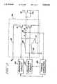
- FIG. 1is a schematic diagram of a conventional gate driver circuit for driving a power MOSFET of a power converter
- FIG. 2is a schematic diagram of a gate driver circuit according to a preferred embodiment of the present invention useful for driving a power MOSFET such as that of FIG. 1;
- FIGS. 3A, 3B, and 3Care graphical illustrations of current and voltage waveforms useful in describing the operation of the driver circuit of FIG. 2;
- FIG. 4is a schematic diagram of a preferred implementation of an ac switch useful in the gate driver circuit of FIG. 2;
- FIGS. 5(A-D)is a timing diagram illustrating appropriate gate drive timing for the driver circuit of FIG. 2 employing the ac switch of FIG. 4.
- a conventional gate driver circuit 12 for driving a power switching device 10 of a power converteris illustrated in FIG. 1.
- the power convertermay be of any type known in the art which employs power semiconductor switching devices which have capacitive gates and generate an output voltage from segments of an input signal, thereby converting ac power to dc, dc power to ac, or dc power to dc, as desired.
- the power switching device 10 shown in FIG. 1may comprise, for example, the single primary-side power switching device of a single-ended power supply. Single-ended converters are described in commonly assigned U.S. Pat. No. 4,845,605 of R. L. Steigerwald, issued on July 4, 1989, which patent is hereby incorporated by reference.
- the conventional driver 12 of FIG. 1comprises two semiconductor switching devices 14 and 16 connected in series in a half-bridge configuration between a positive conductor 18 at the potential of the gate drive voltage supply V s and ground.
- the power switching device 10is illustrated as a MOSFET, but any other type of switching device which has a capacitive gate may be used, such as an insulated gate bipolar transistor (IGBT) or a MOS-controlled thyristor (MCT).
- Switching devices 14 and 16are also illustrated in FIG. 1 as MOSFET's, but any suitable bidirectional switching device may be used, including bipolar junction transistors (BJT's). Therefore, it is by way of example only that device 14 is illustrated as a p-channel type MOSFET and device 16 is illustrated as an n-channel type MOSFET.
- a predriver circuit 22 of a type well-known in the artsuch as a type DS0026 driver manufactured by National Semiconductor Corporation, provides a turn-on signal to the gate of device 14 which, in turn, provides a turn-on signal to the gate of the power MOSFET 10.
- the input capacitance C G of power MOSFET 10charges through device 14 to approximately the gate drive supply voltage level V s . Since the device 14 acts essentially as a resistance while it is conducting, power is dissipated as the input capacitance charges. The amount of energy E dissipated is given by:
- FIG. 2illustrates an improved gate driver circuit 26, according to a preferred embodiment of the present invention, which is useful for driving a power switching device of a power converter, such as power MOSFET 10.
- a series resonant circuitcomprising an inductance 28 and a storage capacitor 30 is coupled to devices 15 and 17 of the half-bridge at the junction therebetween by an ac switch 32.
- Another bidirectional switching device 19is connected in parallel with storage capacitor 30.
- Inductance 28can be implemented, for example, by an inductor having an inductance value in the range of approximately 10 to 20 nanohenries. Such an inductor 28 can be formed from one or two turns of wire having a one centimeter diameter.
- the inductor lead wirescan provide a substantial portion of the desired inductance value Moreover, devices 15 and 17 need not be high current switching devices, in contrast to devices 14 and 16 of the conventional driver circuit, because their function is primarily to hold power MOSFET 10 on or off, as will be described hereinafter.
- resonant transfers of energyare made between the power switching device 10 and the series resonant circuit in a manner to achieve substantially lossless gate driver switching.
- the capacitance of the storage capacitor and the input capacitance of the power MOSFETare preferably equivalent so that these capacitances resonate between substantially the same voltage levels.
- the voltage level across the input capacitance C Gis high, i.e. at approximately the level V s
- power device 10is turned off by closing ac switch 32 so that the gate energy is resonantly discharged through inductor 28 into storage capacitor 30.
- the voltage across storage capacitor 30resonates up to approximately the level V s .
- ac switch 32is opened.
- lower switching device 17is turned on to ensure that power MOSFET 10 remains off, and to ensure that the input capacitance voltage decreases to zero, thereby compensating substantially for any gate losses occurring due to nonideal, i.e. resistive, circuit elements during the resonant transfer of energy.
- ac switch 32In order to turn on power MOSFET 10, ac switch 32 is closed, and the energy stored in storage capacitor 30 is transferred resonantly through inductor 28 to the input capacitance C G of power MOSFET 10. After the energy transfer, ac switch 32 is again opened. Thereafter, upper switching device 15 is turned on to ensure that power MOSFET 10 remains on and to ensure that the input capacitance voltage on power MOSFET 10 again rises to the value V s , thereby compensating substantially for any gate losses occurring during the resonant transfer of energy.
- FIGS. 3A and 3Bgraphically illustrate the gate current and gate (i.e. input capacitance) voltage, respectively, for MOSFET 10 of FIG. 2, while FIG. 3C is a graph of the storage capacitor voltage for the gate driver circuit of FIG. 2.
- the area under curve 36represents the charge stored on input capacitance C G after power MOSFET 10 is turned on
- the substantially equal area under curve 37represents the amount of charge that is removed from the input capacitance after power MOSFET 10 is turned off.
- the storage capacitor voltagereaches approximately a level V s -V 3 , which corresponds to the voltage decrease across the power MOSFET gate as the input capacitance C G discharges before turn-on of device 17, as shown in FIG. 3B.
- the voltage level across storage capacitor 30decreases from the level V S -V 3 to a level V S -V 2 .
- This level V S -V 2corresponds to the voltage increase across the power MOSFET gate as the input capacitance C G charges before device 15 is turned on, as shown in FIG. 3B.
- 3Cis caused by turning on switching device 19 at time t 3 to bring the voltage across the storage capacitor down to zero, thereby compensating for resistive losses in nonideal circuit elements In this way, storage capacitor 30 is fully discharged, thus being ready to accept the resonant charging from the input capacitance C G when power MOSFET 10 is turned off.
- switching device 19is turned off. It is to be noted that in the preferred embodiment of FIG. 2, the gate of switching device 19 is connected to the gate of upper switching device 15 so that both devices are driven by the same predriver circuit 22.
- timing circuitry 40is required to ensure proper gating of the switching devices relative to operation of the ac switch in order to achieve substantially lossless gate switching. That is, timing circuitry 40 is required to provide a time delay between turning on ac switch 32 and turning on the upper and lower switching devices 15 and 17 in the sequences described hereinabove. Furthermore, timing circuitry is needed to coordinate the respective turn-off times of these devices. Suitable timing circuitry may comprise, for example, one-shot timers of a type well-known in the art to provide, for example, a delay on the order of 20 nanoseconds. Alternatively, logic gate delay circuitry may be used to provide the delay.
- FIG. 4A preferred implementation of ac switch 32 is shown in FIG. 4.
- a series combination of a Schottky diode 44 and an n-channel type MOSFET 46is connected in parallel between junctions A and B with a series combination of a Schottky diode 48 and a p-channel type MOSFET 50.
- diodes 44 and 48By employing diodes 44 and 48, precise timing circuitry for opening ac switch 32 is not needed, since these diodes block voltage, thereby preventing any undesirable "ring back" of energy after a resonant energy transfer is complete
- gate driver circuit 52applies a turn-on signal to the gate of device 46 which is positive with respect to the voltage at junction B (thereby holding p-type device 50 off), current flows through diode 44 to power MOSFET 10.
- FIG. 5illustrates appropriate gate drive timing for the driver circuit of FIG. 2 employing the ac switch of FIG. 4.
- the sequence of gating devices 15 and 17 with respect to ac switch 32need not be maintained, since this particular ac switch configuration ensures against any undesirable "ring back" of energy after each resonant transfer of energy.
Landscapes
- Power Conversion In General (AREA)
Abstract
Description
E=1/2C.sub.G V.sub.s.sup.2
E.sub.T =C.sub.G V.sub.S.sup.2
Claims (15)
Priority Applications (1)
| Application Number | Priority Date | Filing Date | Title |
|---|---|---|---|
| US07/447,947US5010261A (en) | 1989-12-08 | 1989-12-08 | Lossless gate driver circuit for a high frequency converter |
Applications Claiming Priority (1)
| Application Number | Priority Date | Filing Date | Title |
|---|---|---|---|
| US07/447,947US5010261A (en) | 1989-12-08 | 1989-12-08 | Lossless gate driver circuit for a high frequency converter |
Publications (1)
| Publication Number | Publication Date |
|---|---|
| US5010261Atrue US5010261A (en) | 1991-04-23 |
Family
ID=23778398
Family Applications (1)
| Application Number | Title | Priority Date | Filing Date |
|---|---|---|---|
| US07/447,947Expired - LifetimeUS5010261A (en) | 1989-12-08 | 1989-12-08 | Lossless gate driver circuit for a high frequency converter |
Country Status (1)
| Country | Link |
|---|---|
| US (1) | US5010261A (en) |
Cited By (57)
| Publication number | Priority date | Publication date | Assignee | Title |
|---|---|---|---|---|
| US5111382A (en)* | 1990-10-23 | 1992-05-05 | Westinghouse Electric Corp. | High power, high frequency resonant inverter using MOS controlled thyristors |
| US5134320A (en)* | 1991-03-07 | 1992-07-28 | Hughes Aircraft Company | High efficiency FET driver with energy recovery |
| US5144154A (en)* | 1990-05-21 | 1992-09-01 | Keithley Instruments, Inc. | Range changing using N and P channel FETS |
| US5204561A (en)* | 1989-07-17 | 1993-04-20 | Sgs-Thomson Microelectronics S.A. | Gate control circuit for mos transistor |
| US5434527A (en)* | 1993-10-25 | 1995-07-18 | Caterpillar Inc. | Gate drive circuit |
| US5475332A (en)* | 1993-01-12 | 1995-12-12 | Mitsubishi Denki Kabushiki Kaisha | Power source circuit |
| US5477184A (en)* | 1992-04-15 | 1995-12-19 | Sanyo Electric Co., Ltd. | Fet switching circuit for switching between a high power transmitting signal and a lower power receiving signal |
| US5497117A (en)* | 1994-03-03 | 1996-03-05 | Kabushiki Kaisha Toshiba | Input sense circuit having selectable thresholds |
| US5532635A (en)* | 1994-09-12 | 1996-07-02 | Harris Corporation | Voltage clamp circuit and method |
| US5546295A (en)* | 1994-02-24 | 1996-08-13 | Rotron Incorporated | Electrical power converter, power supply, and inverter with series-connected switching circuits |
| US5602505A (en)* | 1994-10-28 | 1997-02-11 | Caterpillar Inc. | Gate drive circuit |
| US5673277A (en)* | 1993-09-16 | 1997-09-30 | Quality Semiconductor, Inc. | Scan test circuit using fast transmission gate switch |
| US5697076A (en)* | 1995-05-01 | 1997-12-09 | Illinois Institute Of Technology | Suspended carrier modulation of high-Q transmitters |
| US5804943A (en)* | 1995-05-12 | 1998-09-08 | Texas Instruments Incorporated | Resonant bilateral charging and discharging circuit |
| US5811994A (en)* | 1995-06-30 | 1998-09-22 | Sgs-Thomson Microelectronics, S.R.L. | Electrically controlled bidirectional AC switch, and an integrated circuit and electronic card incorporating the switch |
| US5828261A (en)* | 1996-11-13 | 1998-10-27 | Caterpillar Inc. | Gate drive circuit that controls a power transistor in three states |
| US6084458A (en)* | 1998-01-23 | 2000-07-04 | United Microelectronics Corp. | Bi-directional transistor structure |
| US6107860A (en)* | 1991-12-11 | 2000-08-22 | Vlt Corporation | High efficiency floating gate driver circuit using leakage-inductance transformer |
| US6208195B1 (en) | 1991-03-18 | 2001-03-27 | Integrated Device Technology, Inc. | Fast transmission gate switch |
| US6215350B1 (en)* | 1991-03-18 | 2001-04-10 | Integrated Device Technology, Inc. | Fast transmission gate switch |
| US6441673B1 (en) | 2000-11-06 | 2002-08-27 | General Electric Company | High-frequency resonant gate driver circuit for MOS-gated power switches |
| US6650169B2 (en)* | 2001-10-01 | 2003-11-18 | Koninklijke Philips Electronics N.V. | Gate driver apparatus having an energy recovering circuit |
| US20040080302A1 (en)* | 2002-10-25 | 2004-04-29 | Marvell International Ltd. | Low loss DC/DC converter |
| US20050001659A1 (en)* | 2003-07-02 | 2005-01-06 | Denso Corporation | Gate driving circuit |
| WO2005025065A1 (en)* | 2003-09-08 | 2005-03-17 | Philips Intellectual Property & Standards Gmbh | High frequency control of a semiconductor switch |
| US20050162139A1 (en)* | 2004-01-23 | 2005-07-28 | Mark Hirst | Alternating current switching circuit |
| US20050162870A1 (en)* | 2004-01-23 | 2005-07-28 | Hirst B. M. | Power converter |
| US20050180179A1 (en)* | 2004-02-17 | 2005-08-18 | Hirst B. M. | Snubber ciruit |
| US20060170042A1 (en)* | 2005-01-31 | 2006-08-03 | Zhihua Yang | Resonant gate drive circuits |
| US20060170043A1 (en)* | 2005-01-31 | 2006-08-03 | Yan-Fei Liu | Resonant gate drive circuits |
| US20060186933A1 (en)* | 2005-02-21 | 2006-08-24 | Denso Corporation | Gate driving circuit |
| US20060192437A1 (en)* | 2003-08-01 | 2006-08-31 | Koninklijke Philips Electronics N.V. | High frequency control of a semiconductor switch |
| US20070109025A1 (en)* | 2005-11-04 | 2007-05-17 | Yan-Fei Liu | Resonant gate drive circuit with centre-tapped transformer |
| US20070176585A1 (en)* | 2004-07-13 | 2007-08-02 | Marvell World Trade Ltd. | Closed-loop digital control system for a DC/DC converter |
| US20080180083A1 (en)* | 2006-12-11 | 2008-07-31 | International Rectifier Corporation | Power converter driver with split power supply |
| US7558083B2 (en) | 1997-01-24 | 2009-07-07 | Synqor, Inc. | High efficiency power converter |
| US7564702B2 (en) | 1997-01-24 | 2009-07-21 | Synqor, Inc. | High efficiency power converter |
| US20100019807A1 (en)* | 2008-02-22 | 2010-01-28 | Zhiliang Zhang | Current-source gate driver |
| CN101179227B (en)* | 2002-10-25 | 2010-06-02 | 马维尔国际贸易有限公司 | Low loss dc/dc converter and dc/dc power converting method |
| KR101297460B1 (en)* | 2012-04-24 | 2013-08-16 | 엘에스산전 주식회사 | Apparatus for driving gate |
| US8547143B2 (en) | 2011-01-10 | 2013-10-01 | Yaskawa America, Inc. | Resonant gate drive circuit for a power switching device in a high frequency power converter |
| KR101332991B1 (en)* | 2012-08-24 | 2013-11-25 | 엘에스산전 주식회사 | A gate driver |
| US20140201543A1 (en)* | 2013-01-17 | 2014-07-17 | Dialog Semiconductor Gmbh | Recharging of the Gate Charge of a Transistor |
| EP2569863A4 (en)* | 2010-05-10 | 2014-09-10 | Microsemi Corp | Junction gate driver |
| US9166481B1 (en) | 2013-03-14 | 2015-10-20 | Vlt, Inc. | Digital control of resonant power converters |
| US20160020760A1 (en)* | 2014-07-16 | 2016-01-21 | Hitachi, Ltd. | Switching circuit and semiconductor integrated circuit device |
| EP2874294A4 (en)* | 2012-07-12 | 2016-11-30 | Sony Corp | CONTROL CIRCUIT AND CONTROL METHOD |
| CN106357096A (en)* | 2015-07-14 | 2017-01-25 | 英飞凌科技奥地利有限公司 | System and method for operating switching transistor |
| CN107454993A (en)* | 2017-07-19 | 2017-12-08 | 深圳市汇顶科技股份有限公司 | Power generation circuit, condenser type array sensing device and terminal device |
| JPWO2017110162A1 (en)* | 2015-12-22 | 2018-04-05 | 三菱電機株式会社 | Gate drive circuit and power conversion device including the gate drive circuit |
| US10020752B1 (en) | 2017-09-26 | 2018-07-10 | Vlt, Inc. | Adaptive control of resonant power converters |
| DE102017100972A1 (en) | 2017-01-19 | 2018-07-19 | HELLA GmbH & Co. KGaA | Device for controlling an electronic switching unit |
| US10199950B1 (en) | 2013-07-02 | 2019-02-05 | Vlt, Inc. | Power distribution architecture with series-connected bus converter |
| GB2565274A (en)* | 2017-07-25 | 2019-02-13 | Quepal Ltd | A switch control circuit for a gate drive |
| US20190372467A1 (en)* | 2017-03-21 | 2019-12-05 | Yazaki Corporation | Switching control device |
| US20220311434A1 (en)* | 2021-03-25 | 2022-09-29 | Delta Electronics (Shanghai) Co., Ltd. | Driving device and control method |
| EP4156484A4 (en)* | 2020-06-23 | 2023-11-29 | Huawei Technologies Co., Ltd. | DRIVER CIRCUIT HAVING AN ENERGY RECOVERY FUNCTION AND SWITCHING POWER SUPPLY |
Citations (10)
| Publication number | Priority date | Publication date | Assignee | Title |
|---|---|---|---|---|
| US4224535A (en)* | 1978-08-08 | 1980-09-23 | General Electric Company | Efficient base drive circuit for high current transistors |
| US4492881A (en)* | 1980-09-05 | 1985-01-08 | General Electric Company | Stored charge inverter circuit |
| US4575642A (en)* | 1982-04-07 | 1986-03-11 | International Standard Electric Corporation | Control circuit for an integrated device |
| US4612451A (en)* | 1983-02-25 | 1986-09-16 | Hitachi, Ltd. | Drive circuit for driving a transistor |
| US4626715A (en)* | 1983-02-28 | 1986-12-02 | Pioneer Electronic Corporation | MOS FET amplifier output stage |
| US4783601A (en)* | 1986-06-17 | 1988-11-08 | U.S. Philips Corporation | Integrated logic circuit having a control circuit for generating a time-dependent waveform |
| US4791321A (en)* | 1985-12-27 | 1988-12-13 | Kabushiki Kaisha Toshiba | CMOS output circuit device |
| US4825101A (en)* | 1988-02-11 | 1989-04-25 | Advanced Micro Devices, Inc. | Full-level, fast CMOS output buffer |
| US4845389A (en)* | 1987-03-06 | 1989-07-04 | U.S. Philips Corporation | Very high frequency mixer |
| US4845605A (en)* | 1988-06-27 | 1989-07-04 | General Electric Company | High-frequency DC-DC power converter with zero-voltage switching of single primary-side power device |
- 1989
- 1989-12-08USUS07/447,947patent/US5010261A/ennot_activeExpired - Lifetime
Patent Citations (10)
| Publication number | Priority date | Publication date | Assignee | Title |
|---|---|---|---|---|
| US4224535A (en)* | 1978-08-08 | 1980-09-23 | General Electric Company | Efficient base drive circuit for high current transistors |
| US4492881A (en)* | 1980-09-05 | 1985-01-08 | General Electric Company | Stored charge inverter circuit |
| US4575642A (en)* | 1982-04-07 | 1986-03-11 | International Standard Electric Corporation | Control circuit for an integrated device |
| US4612451A (en)* | 1983-02-25 | 1986-09-16 | Hitachi, Ltd. | Drive circuit for driving a transistor |
| US4626715A (en)* | 1983-02-28 | 1986-12-02 | Pioneer Electronic Corporation | MOS FET amplifier output stage |
| US4791321A (en)* | 1985-12-27 | 1988-12-13 | Kabushiki Kaisha Toshiba | CMOS output circuit device |
| US4783601A (en)* | 1986-06-17 | 1988-11-08 | U.S. Philips Corporation | Integrated logic circuit having a control circuit for generating a time-dependent waveform |
| US4845389A (en)* | 1987-03-06 | 1989-07-04 | U.S. Philips Corporation | Very high frequency mixer |
| US4825101A (en)* | 1988-02-11 | 1989-04-25 | Advanced Micro Devices, Inc. | Full-level, fast CMOS output buffer |
| US4845605A (en)* | 1988-06-27 | 1989-07-04 | General Electric Company | High-frequency DC-DC power converter with zero-voltage switching of single primary-side power device |
Non-Patent Citations (2)
| Title |
|---|
| W. A. Tabisz et al., "Zero-Voltage-Switched Quasi-Resonant Buck and Flyback Converters--Experimental Results at 10 MHz", Power Electronics Specialists Conference Record, pp. 404-413. |
| W. A. Tabisz et al., Zero Voltage Switched Quasi Resonant Buck and Flyback Converters Experimental Results at 10 MHz , Power Electronics Specialists Conference Record, pp. 404 413.* |
Cited By (103)
| Publication number | Priority date | Publication date | Assignee | Title |
|---|---|---|---|---|
| US5204561A (en)* | 1989-07-17 | 1993-04-20 | Sgs-Thomson Microelectronics S.A. | Gate control circuit for mos transistor |
| US5144154A (en)* | 1990-05-21 | 1992-09-01 | Keithley Instruments, Inc. | Range changing using N and P channel FETS |
| US5111382A (en)* | 1990-10-23 | 1992-05-05 | Westinghouse Electric Corp. | High power, high frequency resonant inverter using MOS controlled thyristors |
| US5134320A (en)* | 1991-03-07 | 1992-07-28 | Hughes Aircraft Company | High efficiency FET driver with energy recovery |
| US6556063B2 (en) | 1991-03-18 | 2003-04-29 | Integrated Device Technology, Inc. | Fast transmission gate switch |
| US6208195B1 (en) | 1991-03-18 | 2001-03-27 | Integrated Device Technology, Inc. | Fast transmission gate switch |
| US6215350B1 (en)* | 1991-03-18 | 2001-04-10 | Integrated Device Technology, Inc. | Fast transmission gate switch |
| US6107860A (en)* | 1991-12-11 | 2000-08-22 | Vlt Corporation | High efficiency floating gate driver circuit using leakage-inductance transformer |
| US5477184A (en)* | 1992-04-15 | 1995-12-19 | Sanyo Electric Co., Ltd. | Fet switching circuit for switching between a high power transmitting signal and a lower power receiving signal |
| US5475332A (en)* | 1993-01-12 | 1995-12-12 | Mitsubishi Denki Kabushiki Kaisha | Power source circuit |
| US5673277A (en)* | 1993-09-16 | 1997-09-30 | Quality Semiconductor, Inc. | Scan test circuit using fast transmission gate switch |
| US5434527A (en)* | 1993-10-25 | 1995-07-18 | Caterpillar Inc. | Gate drive circuit |
| US5546295A (en)* | 1994-02-24 | 1996-08-13 | Rotron Incorporated | Electrical power converter, power supply, and inverter with series-connected switching circuits |
| US5497117A (en)* | 1994-03-03 | 1996-03-05 | Kabushiki Kaisha Toshiba | Input sense circuit having selectable thresholds |
| US5532635A (en)* | 1994-09-12 | 1996-07-02 | Harris Corporation | Voltage clamp circuit and method |
| US5602505A (en)* | 1994-10-28 | 1997-02-11 | Caterpillar Inc. | Gate drive circuit |
| US5697076A (en)* | 1995-05-01 | 1997-12-09 | Illinois Institute Of Technology | Suspended carrier modulation of high-Q transmitters |
| US5804943A (en)* | 1995-05-12 | 1998-09-08 | Texas Instruments Incorporated | Resonant bilateral charging and discharging circuit |
| US5811994A (en)* | 1995-06-30 | 1998-09-22 | Sgs-Thomson Microelectronics, S.R.L. | Electrically controlled bidirectional AC switch, and an integrated circuit and electronic card incorporating the switch |
| US5828261A (en)* | 1996-11-13 | 1998-10-27 | Caterpillar Inc. | Gate drive circuit that controls a power transistor in three states |
| US8023290B2 (en) | 1997-01-24 | 2011-09-20 | Synqor, Inc. | High efficiency power converter |
| US8493751B2 (en) | 1997-01-24 | 2013-07-23 | Synqor, Inc. | High efficiency power converter |
| US7558083B2 (en) | 1997-01-24 | 2009-07-07 | Synqor, Inc. | High efficiency power converter |
| US7564702B2 (en) | 1997-01-24 | 2009-07-21 | Synqor, Inc. | High efficiency power converter |
| US9143042B2 (en) | 1997-01-24 | 2015-09-22 | Synqor, Inc. | High efficiency power converter |
| US6084458A (en)* | 1998-01-23 | 2000-07-04 | United Microelectronics Corp. | Bi-directional transistor structure |
| US6441673B1 (en) | 2000-11-06 | 2002-08-27 | General Electric Company | High-frequency resonant gate driver circuit for MOS-gated power switches |
| US6650169B2 (en)* | 2001-10-01 | 2003-11-18 | Koninklijke Philips Electronics N.V. | Gate driver apparatus having an energy recovering circuit |
| US20050237046A1 (en)* | 2002-10-25 | 2005-10-27 | Marvell World Trade Ltd. | Low loss DC/DC converter |
| US7148673B2 (en) | 2002-10-25 | 2006-12-12 | Marvell World Trade Ltd. | Method and apparatus including low loss DC/DC converter |
| US7271573B2 (en) | 2002-10-25 | 2007-09-18 | Marvell World Trade Ltd. | Low loss DC/DC converter including a multi-level controller that applies a monotonic sequence of voltage levels |
| EP1414143A3 (en)* | 2002-10-25 | 2005-01-12 | Marvell World Trade Ltd. | Low loss DC/DC converter |
| CN101179227B (en)* | 2002-10-25 | 2010-06-02 | 马维尔国际贸易有限公司 | Low loss dc/dc converter and dc/dc power converting method |
| CN100352152C (en)* | 2002-10-25 | 2007-11-28 | 马维尔国际贸易有限公司 | Low-loss DC/DC converter and DC-to-DC power conversion method |
| US20040080302A1 (en)* | 2002-10-25 | 2004-04-29 | Marvell International Ltd. | Low loss DC/DC converter |
| US7161342B2 (en) | 2002-10-25 | 2007-01-09 | Marvell World Trade Ltd. | Low loss DC/DC converter |
| CN101179226B (en)* | 2002-10-25 | 2012-06-20 | 马维尔国际贸易有限公司 | Low loss dc/dc converter and dc/dc power converting method |
| US20060273778A1 (en)* | 2002-10-25 | 2006-12-07 | Marvell World Trade Ltd. | Low loss DC/DC converter |
| US20050001659A1 (en)* | 2003-07-02 | 2005-01-06 | Denso Corporation | Gate driving circuit |
| US7091753B2 (en) | 2003-07-02 | 2006-08-15 | Denso Corporation | Gate driving circuit |
| FR2857177A1 (en)* | 2003-07-02 | 2005-01-07 | Denso Corp | GATE ATTACK CIRCUIT |
| US20060192437A1 (en)* | 2003-08-01 | 2006-08-31 | Koninklijke Philips Electronics N.V. | High frequency control of a semiconductor switch |
| US7602229B2 (en) | 2003-09-08 | 2009-10-13 | Koninklijke Philips Electronics N.V. | High frequency control of a semiconductor switch |
| JP2007505544A (en)* | 2003-09-08 | 2007-03-08 | コニンクリユケ フィリップス エレクトロニクス エヌ.ブイ. | High frequency control of semiconductor switches |
| WO2005025065A1 (en)* | 2003-09-08 | 2005-03-17 | Philips Intellectual Property & Standards Gmbh | High frequency control of a semiconductor switch |
| JP4763606B2 (en)* | 2003-09-08 | 2011-08-31 | コーニンクレッカ フィリップス エレクトロニクス エヌ ヴィ | High frequency control of semiconductor switches |
| US20050162139A1 (en)* | 2004-01-23 | 2005-07-28 | Mark Hirst | Alternating current switching circuit |
| US20050162870A1 (en)* | 2004-01-23 | 2005-07-28 | Hirst B. M. | Power converter |
| US8253394B2 (en) | 2004-02-17 | 2012-08-28 | Hewlett-Packard Development Company, L.P. | Snubber circuit |
| US20050180179A1 (en)* | 2004-02-17 | 2005-08-18 | Hirst B. M. | Snubber ciruit |
| US7679347B2 (en) | 2004-07-13 | 2010-03-16 | Marvell World Trade Ltd. | Closed-loop digital control system for a DC/DC converter |
| US8183846B2 (en) | 2004-07-13 | 2012-05-22 | Marvell World Trade Ltd. | Method and apparatus for controlling a DC/DC converter |
| US20070176585A1 (en)* | 2004-07-13 | 2007-08-02 | Marvell World Trade Ltd. | Closed-loop digital control system for a DC/DC converter |
| US20100171478A1 (en)* | 2004-07-13 | 2010-07-08 | Runsheng He | Closed-loop digital control system for a dc/dc converter |
| US20060170042A1 (en)* | 2005-01-31 | 2006-08-03 | Zhihua Yang | Resonant gate drive circuits |
| US7612602B2 (en) | 2005-01-31 | 2009-11-03 | Queen's University At Kingston | Resonant gate drive circuits |
| US20060170043A1 (en)* | 2005-01-31 | 2006-08-03 | Yan-Fei Liu | Resonant gate drive circuits |
| US7598792B2 (en) | 2005-01-31 | 2009-10-06 | Queen's University At Kingston | Resonant gate drive circuits |
| US7365579B2 (en)* | 2005-02-21 | 2008-04-29 | Denso Corporation | Gate driving circuit |
| US20060186933A1 (en)* | 2005-02-21 | 2006-08-24 | Denso Corporation | Gate driving circuit |
| US20070109025A1 (en)* | 2005-11-04 | 2007-05-17 | Yan-Fei Liu | Resonant gate drive circuit with centre-tapped transformer |
| US7453292B2 (en) | 2005-11-04 | 2008-11-18 | Queen's University At Kingston | Resonant gate drive circuit with centre-tapped transformer |
| US8063613B2 (en)* | 2006-12-11 | 2011-11-22 | International Rectifier Corporation | Power converter driver with split power supply |
| US20080180083A1 (en)* | 2006-12-11 | 2008-07-31 | International Rectifier Corporation | Power converter driver with split power supply |
| US20100019807A1 (en)* | 2008-02-22 | 2010-01-28 | Zhiliang Zhang | Current-source gate driver |
| US8085083B2 (en)* | 2008-02-22 | 2011-12-27 | Queen's University At Kingston | Current-source gate driver |
| EP2569863A4 (en)* | 2010-05-10 | 2014-09-10 | Microsemi Corp | Junction gate driver |
| US8547143B2 (en) | 2011-01-10 | 2013-10-01 | Yaskawa America, Inc. | Resonant gate drive circuit for a power switching device in a high frequency power converter |
| KR101297460B1 (en)* | 2012-04-24 | 2013-08-16 | 엘에스산전 주식회사 | Apparatus for driving gate |
| US8760200B2 (en) | 2012-04-24 | 2014-06-24 | Lsis Co., Ltd. | Gate driving apparatus |
| EP2874294A4 (en)* | 2012-07-12 | 2016-11-30 | Sony Corp | CONTROL CIRCUIT AND CONTROL METHOD |
| KR101332991B1 (en)* | 2012-08-24 | 2013-11-25 | 엘에스산전 주식회사 | A gate driver |
| US20140201543A1 (en)* | 2013-01-17 | 2014-07-17 | Dialog Semiconductor Gmbh | Recharging of the Gate Charge of a Transistor |
| US8872576B2 (en)* | 2013-01-17 | 2014-10-28 | Dialog Semiconductor Gmbh | Recharging of the gate charge of a transistor |
| US9166481B1 (en) | 2013-03-14 | 2015-10-20 | Vlt, Inc. | Digital control of resonant power converters |
| US11075583B1 (en) | 2013-07-02 | 2021-07-27 | Vicor Corporation | Power distribution architecture with series-connected bus converter |
| US12395087B1 (en) | 2013-07-02 | 2025-08-19 | Vicor Corporation | Power distribution architecture with series-connected bus converter |
| US10594223B1 (en) | 2013-07-02 | 2020-03-17 | Vlt, Inc. | Power distribution architecture with series-connected bus converter |
| US11705820B2 (en) | 2013-07-02 | 2023-07-18 | Vicor Corporation | Power distribution architecture with series-connected bus converter |
| US10199950B1 (en) | 2013-07-02 | 2019-02-05 | Vlt, Inc. | Power distribution architecture with series-connected bus converter |
| US20160020760A1 (en)* | 2014-07-16 | 2016-01-21 | Hitachi, Ltd. | Switching circuit and semiconductor integrated circuit device |
| US9337823B2 (en)* | 2014-07-16 | 2016-05-10 | Hitachi, Ltd. | Switching circuit and semiconductor integrated circuit device |
| CN106357096B (en)* | 2015-07-14 | 2019-07-19 | 英飞凌科技奥地利有限公司 | The system and method for Operation switch transistor |
| CN106357096A (en)* | 2015-07-14 | 2017-01-25 | 英飞凌科技奥地利有限公司 | System and method for operating switching transistor |
| JPWO2017110162A1 (en)* | 2015-12-22 | 2018-04-05 | 三菱電機株式会社 | Gate drive circuit and power conversion device including the gate drive circuit |
| DE102017100972A1 (en) | 2017-01-19 | 2018-07-19 | HELLA GmbH & Co. KGaA | Device for controlling an electronic switching unit |
| US11070201B2 (en) | 2017-01-19 | 2021-07-20 | HELLA GmbH & Co. KGaA | Apparatus for controlling an electronic switching unit |
| US20190372467A1 (en)* | 2017-03-21 | 2019-12-05 | Yazaki Corporation | Switching control device |
| US10770984B2 (en)* | 2017-03-21 | 2020-09-08 | Yazaki Corporation | Switching control device with reverse bias circuit |
| EP3457570A4 (en)* | 2017-07-19 | 2019-07-10 | Shenzhen Goodix Technology Co., Ltd. | POWER SUPPLY GENERATING CIRCUIT, CAPACITIVE TYPE NETWORK DETECTING APPARATUS, AND TERMINAL DEVICE |
| US10921158B2 (en) | 2017-07-19 | 2021-02-16 | Shenzhen GOODIX Technology Co., Ltd. | Power supply generating circuit, capacitive array sensing apparatus and terminal device |
| CN107454993A (en)* | 2017-07-19 | 2017-12-08 | 深圳市汇顶科技股份有限公司 | Power generation circuit, condenser type array sensing device and terminal device |
| GB2565274A (en)* | 2017-07-25 | 2019-02-13 | Quepal Ltd | A switch control circuit for a gate drive |
| US10637364B1 (en) | 2017-09-26 | 2020-04-28 | Vlt, Inc. | Adaptive control of resonant power converters |
| US11018594B1 (en) | 2017-09-26 | 2021-05-25 | Vicor Corporation | Adaptive control of resonant power converters |
| US10153704B1 (en) | 2017-09-26 | 2018-12-11 | Vlt, Inc. | Adaptive control of resonant power converters |
| US11831246B1 (en) | 2017-09-26 | 2023-11-28 | Vicor Corporation | Adaptive control of resonant power converters |
| US12132409B1 (en) | 2017-09-26 | 2024-10-29 | Vicor Corporation | Adaptive control of resonant power converters |
| US10020752B1 (en) | 2017-09-26 | 2018-07-10 | Vlt, Inc. | Adaptive control of resonant power converters |
| EP4156484A4 (en)* | 2020-06-23 | 2023-11-29 | Huawei Technologies Co., Ltd. | DRIVER CIRCUIT HAVING AN ENERGY RECOVERY FUNCTION AND SWITCHING POWER SUPPLY |
| US12231034B2 (en) | 2020-06-23 | 2025-02-18 | Huawei Technologies Co., Ltd. | Drive circuit with energy recovery function and switch mode power supply |
| US20220311434A1 (en)* | 2021-03-25 | 2022-09-29 | Delta Electronics (Shanghai) Co., Ltd. | Driving device and control method |
| US11671093B2 (en)* | 2021-03-25 | 2023-06-06 | Delta Electronics (Shanghai) Co., Ltd. | Driving device and control method |
Similar Documents
| Publication | Publication Date | Title |
|---|---|---|
| US5010261A (en) | Lossless gate driver circuit for a high frequency converter | |
| US20220085801A1 (en) | Efficient igbt switching | |
| US4967109A (en) | High efficiency gate driver circuit for a high frequency converter | |
| De Vries | A resonant power MOSFET/IGBT gate driver | |
| JP3666843B2 (en) | Gate circuit of insulated gate semiconductor device | |
| US6094087A (en) | Gate drive circuit for isolated gate devices and method of operation thereof | |
| US6441673B1 (en) | High-frequency resonant gate driver circuit for MOS-gated power switches | |
| US6839246B1 (en) | Self-driving circuit for a DC/DC converter | |
| US11652399B2 (en) | Miller clamp protection circuit, driving circuit, driving chip and intelligent IGBT module | |
| Conrad et al. | Avoiding reverse recovery effects in super junction MOSFET based half-bridges | |
| CN113497610A (en) | Gate drive circuit capable of reducing conduction loss of power semiconductor | |
| US7248093B2 (en) | Bipolar bootstrap top switch gate drive for half-bridge semiconductor power topologies | |
| Ma | Driving GaN power transistors | |
| EP3872990A1 (en) | Semiconductor switching assembly and gate driver circuit | |
| US5886563A (en) | Interlocked half-bridge circuit | |
| US5134320A (en) | High efficiency FET driver with energy recovery | |
| US6580255B1 (en) | Adaptive gate drivers for zero voltage switching power conversion circuits | |
| US7023246B2 (en) | Driving circuit for a control terminal of a bipolar transistor in an emitter-switching configuration having a resonant load | |
| US5493247A (en) | Gate circuit for hard driven GTO | |
| US6774682B2 (en) | Circuit configuration for driving a semiconductor switching element and method for same | |
| US6268754B1 (en) | Gate driving circuit for power semiconductor switch | |
| JP2000197343A (en) | Gate control method for semiconductor device | |
| US4001607A (en) | Drive circuit for a gate semiconductor device | |
| JP2004088892A (en) | Gate circuit of insulated gate semiconductor device | |
| US20250260304A1 (en) | Gate Driving Circuit for Wide Bandgap (WBG) Power Devices |
Legal Events
| Date | Code | Title | Description |
|---|---|---|---|
| AS | Assignment | Owner name:GENERAL ELECTRIC COMPANY, A CORP. OF NY., NEW YORK Free format text:ASSIGNMENT OF ASSIGNORS INTEREST.;ASSIGNOR:STEIGERWALD, ROBERT L.;REEL/FRAME:005193/0298 Effective date:19891130 | |
| FEPP | Fee payment procedure | Free format text:PAYOR NUMBER ASSIGNED (ORIGINAL EVENT CODE: ASPN); ENTITY STATUS OF PATENT OWNER: LARGE ENTITY | |
| STCF | Information on status: patent grant | Free format text:PATENTED CASE | |
| AS | Assignment | Owner name:NORTH AMERICAN POWER SUPPLIES, INC., A CORP. OF IN Free format text:ASSIGNMENT OF ASSIGNORS INTEREST.;ASSIGNOR:GENERAL ELECTRIC COMPANY, A NY CORP.;REEL/FRAME:006080/0673 Effective date:19920107 | |
| FPAY | Fee payment | Year of fee payment:4 | |
| AS | Assignment | Owner name:NORWEST BANK OF MINNESOTA, NATIONAL ASSOCIATION, M Free format text:SECURITY AGREEMENT;ASSIGNOR:NORTHERN AMERICAN POWER SUPPLIES, INC.;REEL/FRAME:007894/0422 Effective date:19960325 | |
| AS | Assignment | Owner name:NORWEST BANK MINNESOTA, NATIONAL ASSOCIATION, MINN Free format text:SECURITY AGREEMENT;ASSIGNOR:NORTH AMERICAN POWER SUPPLIES, INC.;REEL/FRAME:008146/0407 Effective date:19960912 | |
| FPAY | Fee payment | Year of fee payment:8 | |
| FPAY | Fee payment | Year of fee payment:12 |