US5008900A - Subscriber unit for wireless digital subscriber communication system - Google Patents
Subscriber unit for wireless digital subscriber communication systemDownload PDFInfo
- Publication number
- US5008900A US5008900AUS07/394,497US39449789AUS5008900AUS 5008900 AUS5008900 AUS 5008900AUS 39449789 AUS39449789 AUS 39449789AUS 5008900 AUS5008900 AUS 5008900A
- Authority
- US
- United States
- Prior art keywords
- digital
- chip
- signal
- symbols
- base station
- Prior art date
- Legal status (The legal status is an assumption and is not a legal conclusion. Google has not performed a legal analysis and makes no representation as to the accuracy of the status listed.)
- Expired - Lifetime
Links
- 238000004891communicationMethods0.000titleclaimsabstractdescription16
- 230000002194synthesizing effectEffects0.000claimsabstractdescription23
- 230000005540biological transmissionEffects0.000claimsabstractdescription13
- 239000000872bufferSubstances0.000claimsdescription39
- 238000012545processingMethods0.000claimsdescription38
- 238000001914filtrationMethods0.000claimsdescription19
- 230000004044responseEffects0.000claimsdescription7
- 238000000034methodMethods0.000abstractdescription29
- 230000008569processEffects0.000abstractdescription17
- 230000015572biosynthetic processEffects0.000abstractdescription8
- 238000003786synthesis reactionMethods0.000abstractdescription8
- 230000006870functionEffects0.000description42
- 108091006146ChannelsProteins0.000description28
- 101001096074Homo sapiens Regenerating islet-derived protein 4Proteins0.000description20
- 102100037889Regenerating islet-derived protein 4Human genes0.000description20
- 240000007320Pinus strobusSpecies0.000description19
- 239000012723sample bufferSubstances0.000description12
- 230000001360synchronised effectEffects0.000description10
- 239000003550markerSubstances0.000description8
- 238000012544monitoring processMethods0.000description8
- 238000012549trainingMethods0.000description8
- 238000009825accumulationMethods0.000description6
- 238000007792additionMethods0.000description6
- 230000000295complement effectEffects0.000description5
- 238000001514detection methodMethods0.000description5
- 230000000694effectsEffects0.000description4
- 238000012986modificationMethods0.000description4
- 230000004048modificationEffects0.000description4
- 238000013139quantizationMethods0.000description4
- 239000000523sampleSubstances0.000description4
- 230000003139buffering effectEffects0.000description3
- 238000010586diagramMethods0.000description3
- 238000011068loading methodMethods0.000description3
- 230000010363phase shiftEffects0.000description3
- 238000004458analytical methodMethods0.000description2
- 238000004364calculation methodMethods0.000description2
- 230000008859changeEffects0.000description2
- 230000006835compressionEffects0.000description2
- 238000007906compressionMethods0.000description2
- 238000000354decomposition reactionMethods0.000description2
- 230000007423decreaseEffects0.000description2
- 230000003111delayed effectEffects0.000description2
- 230000010354integrationEffects0.000description2
- 238000004519manufacturing processMethods0.000description2
- 239000011159matrix materialSubstances0.000description2
- 238000002156mixingMethods0.000description2
- 238000011084recoveryMethods0.000description2
- 238000005070samplingMethods0.000description2
- 230000011664signalingEffects0.000description2
- 238000001228spectrumMethods0.000description2
- 238000012360testing methodMethods0.000description2
- 238000012546transferMethods0.000description2
- 238000013459approachMethods0.000description1
- 239000002131composite materialSubstances0.000description1
- 125000004122cyclic groupChemical group0.000description1
- 238000013461designMethods0.000description1
- 230000009977dual effectEffects0.000description1
- 238000011049fillingMethods0.000description1
- 238000009432framingMethods0.000description1
- 230000010365information processingEffects0.000description1
- 230000000977initiatory effectEffects0.000description1
- 230000000630rising effectEffects0.000description1
- 238000010845search algorithmMethods0.000description1
- 238000007493shaping processMethods0.000description1
- 230000003595spectral effectEffects0.000description1
- 230000007704transitionEffects0.000description1
Images


Classifications
- H—ELECTRICITY
- H03—ELECTRONIC CIRCUITRY
- H03C—MODULATION
- H03C3/00—Angle modulation
- H—ELECTRICITY
- H04—ELECTRIC COMMUNICATION TECHNIQUE
- H04W—WIRELESS COMMUNICATION NETWORKS
- H04W88/00—Devices specially adapted for wireless communication networks, e.g. terminals, base stations or access point devices
- H04W88/02—Terminal devices
- H—ELECTRICITY
- H03—ELECTRONIC CIRCUITRY
- H03B—GENERATION OF OSCILLATIONS, DIRECTLY OR BY FREQUENCY-CHANGING, BY CIRCUITS EMPLOYING ACTIVE ELEMENTS WHICH OPERATE IN A NON-SWITCHING MANNER; GENERATION OF NOISE BY SUCH CIRCUITS
- H03B28/00—Generation of oscillations by methods not covered by groups H03B5/00 - H03B27/00, including modification of the waveform to produce sinusoidal oscillations
- H—ELECTRICITY
- H03—ELECTRONIC CIRCUITRY
- H03D—DEMODULATION OR TRANSFERENCE OF MODULATION FROM ONE CARRIER TO ANOTHER
- H03D3/00—Demodulation of angle-, frequency- or phase- modulated oscillations
- H03D3/007—Demodulation of angle-, frequency- or phase- modulated oscillations by converting the oscillations into two quadrature related signals
- H—ELECTRICITY
- H04—ELECTRIC COMMUNICATION TECHNIQUE
- H04L—TRANSMISSION OF DIGITAL INFORMATION, e.g. TELEGRAPHIC COMMUNICATION
- H04L27/00—Modulated-carrier systems
- H—ELECTRICITY
- H04—ELECTRIC COMMUNICATION TECHNIQUE
- H04L—TRANSMISSION OF DIGITAL INFORMATION, e.g. TELEGRAPHIC COMMUNICATION
- H04L27/00—Modulated-carrier systems
- H04L27/18—Phase-modulated carrier systems, i.e. using phase-shift keying
- H04L27/20—Modulator circuits; Transmitter circuits
- H04L27/2032—Modulator circuits; Transmitter circuits for discrete phase modulation, e.g. in which the phase of the carrier is modulated in a nominally instantaneous manner
- H04L27/2092—Modulator circuits; Transmitter circuits for discrete phase modulation, e.g. in which the phase of the carrier is modulated in a nominally instantaneous manner with digital generation of the modulated carrier (does not include the modulation of a digitally generated carrier)
- H—ELECTRICITY
- H04—ELECTRIC COMMUNICATION TECHNIQUE
- H04W—WIRELESS COMMUNICATION NETWORKS
- H04W56/00—Synchronisation arrangements
- H—ELECTRICITY
- H04—ELECTRIC COMMUNICATION TECHNIQUE
- H04L—TRANSMISSION OF DIGITAL INFORMATION, e.g. TELEGRAPHIC COMMUNICATION
- H04L25/00—Baseband systems
- H04L25/02—Details ; arrangements for supplying electrical power along data transmission lines
- H04L25/03—Shaping networks in transmitter or receiver, e.g. adaptive shaping networks
- H04L25/03006—Arrangements for removing intersymbol interference
- H04L2025/0335—Arrangements for removing intersymbol interference characterised by the type of transmission
- H04L2025/03375—Passband transmission
- H—ELECTRICITY
- H04—ELECTRIC COMMUNICATION TECHNIQUE
- H04L—TRANSMISSION OF DIGITAL INFORMATION, e.g. TELEGRAPHIC COMMUNICATION
- H04L25/00—Baseband systems
- H04L25/02—Details ; arrangements for supplying electrical power along data transmission lines
- H04L25/03—Shaping networks in transmitter or receiver, e.g. adaptive shaping networks
- H04L25/03006—Arrangements for removing intersymbol interference
- H04L2025/03433—Arrangements for removing intersymbol interference characterised by equaliser structure
- H04L2025/03439—Fixed structures
- H04L2025/03445—Time domain
- H04L2025/03471—Tapped delay lines
- H04L2025/03477—Tapped delay lines not time-recursive
Definitions
- the present inventiongenerally pertains to subscriber communications systems and is particularly directed to an improved subscriber unit for wireless communication with a base station in a wireless digital subscriber communication system.
- a typical subscriber unitis described in U.S. patent application Ser. No. 06/893,916 filed Aug. 7, 1986 by David N. Critchlow et al. now issued as U.S. Pat. No. 4,825,448, dated Apr. 25, 1989.
- a base station used with such a subscriber unit in a wireless digital subscriber communication systemis described in U.S. Pat. No. 4,777,633 to Thomas E. Fletcher, Wendeline R. Avis, Gregory T. Saffee and Karle J. Johnson.
- 4,825,448includes means for transcoding a digital voice input signal to provide digital input symbols; means for FIR filtering the digital input symbols; means for deriving an analog intermediate frequency input signal from the filtered input symbols; means for combining the intermediate frequency input signal with an RF carrier for radio transmission to the base station; means for demodulating an output signal received from the base station to provide digital output symbols; and means for synthesizing a digital voice output signal from the digital output symbols.
- the subscriber unitincludes a baseband processor chip and a modem processor chip. Both are TMS32020 digital signal processors.
- the baseband processor chipsperform the transcoding of the digital voice input signal, the synthesis of the digital output symbols, and various baseband control functions; and the modem processor chip performs the FIR filtering of the digital input symbols, and the demodulation of the output signal received from the base station.
- the modem processor chipgenerally acts as the master for the system.
- the present inventionprovides a less expensive subscriber unit.
- the subscriber unit of the present inventionincludes means for transcoding a digital voice input signal to provide digital input symbols; means for FIR filtering the digital input symbols; means for modulating a digital intermediate frequency signal with the filtered input symbols to provide a modulated intermediate frequency input signal; means for processing the modulated input signal for transmission to the base station; means for demodulating an output signal received from the base station to provide digital output symbols; and means for synthesizing a digital voice output signal from the digital output symbols; wherein the subscriber unit includes a FIR chip for performing said FIR filtering of the digital input symbols; a DIF chip for digitally synthesizing said digital intermediate frequency signal and for performing said modulation of said digital intermediate frequency signal; and a single processor chip for performing said transcoding of said digital voice input signal, for performing said demodulation of said output signal received from the base station, and for performing said synthesizing of the digital output symbols.
- the FIR chipperforms the FIR filtering function that was implemented by software in the modem processor of the prior art subscriber unit described above. By moving the time consuming transmit FIR filtering function out of the modem processor and by performing the demodulation function with the same processor that performs the baseband processing function, only one processor chip is required.
- the means for digitally synthesizing the digital intermediate frequency signalis a direct digital synthesizer (DDS) which include means coupled to the processor chip for accumulating phase data provided by the processor chip to indicate a predetermined intermediate frequency; and means for processing the accumulated phase data to generate said digital intermediate frequency signal at the predetermined intermediate frequency.
- DDSdirect digital synthesizer
- the DIF chipprovides a fully modulated digital IF signal that can be digitally synthesized at any one of a plurality of different predetermined IF frequencies; and fine resolution frequency adjustment can be provided in the DIF chip to allow frequency tracking of the output signal received from the base station.
- a direct digital synthesizeris stable and easy to produce. Phase noise specifications can be met without the need for an expensive and complex PLL RF synthesizer.
- the DDS featureprovides frequency agility within the IF band and provides easier frequency modifications for operation in other bands.
- the FIR chipincludes means for generating timing signals for timing the transcoding operation and the operation of synthesizing the digital voice output signal by the processor chip.
- the processor chipperforms the demodulation of the output signal received from the base station independently of the timing signals generated by the FIR chip.
- the processor chipreceives said output signal in accordance with the timing signals generated by the FIR chip, and buffers the received output signal for demodulation, thereby allowing the processor chip to perform said demodulation when not performing said transcoding and synthesizing operations.
- the present inventionalso reduces manufacturing costs by including a combination of a slow memory coupled to the processor chip for storing processing codes used by the processor chip when said codes need not be operated with zero wait states; and a fast memory coupled to the processor chip for temporarily storing processing codes used by the processor chip when said codes are operated with zero wait states.
- Fast RAMswith a zero wait state
- fast EPROMswith the same chip density are very expensive.
- the processor codescan be stored in a slow EPROM (with one or more wait states), and when procedures must be run with zero wait states, the code can be uploaded from the slow memory to the fast memory and run from there.
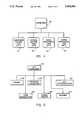
- FIG. 1is a block diagram of a preferred embodiment of the subscriber unit of the present invention.
- FIG. 2is a block diagram of the FIR chip included in the embodiment shown in FIG. 1.
- FIG. 3is a block diagram of the DIF chip included in the embodiment shown in FIG. 1.
- FIG. 4illustrates the processing tasks performed by the processor chip shown in the embodiment of FIG. 1.
- FIG. 5illustrates the processing routines included in modem processing task shown in FIG. 4.
- A/DAnalog to Digital
- AGCAutomatic Gain Control
- ASICApplication Specific Integrated Circuit
- EPROMErasable Read Only Memory
- PCMPulse Code Modulation
- RAMRandom Access Memory
- RCCRadio Control Channel
- a preferred embodiment of the subscriber unit of the present inventionincludes a telephone interface circuit 10, a SLIC and codec circuit 11, a processor chip 12, a fast memory 13, a slow memory 14, an address decoder 15, a FIR chip 16, a DIF chip 17, a DAC 18, an A/D converter 19, a radio 20, a ringer circuit 21, and an oscillator 22.
- the FIR chip 16which is an ASIC chip, is interfaced to the DIF chip 17 by lines 23 and 24, to the processor chip 12 by processor bus 25 and line 26, to the A/D converter 19 by line 27, to the SLIC and codec circuit 11 by line 29, to the radio 20 by line 30, and to the ringer circuit 21 by line 31.
- the telephone interface circuit 10is interfaced with a telephone 32, which converts sound waves into an input voice signal, and converts an output voice signal into sound waves.
- the SLIC and codec circuit 11is coupled to the telephone interface circuit 10 for converting the input voice signal into a baseband digital input signal, which is provided to the processor chip 12.
- the processor chipis also interfaced directly with an UART for alternatively receiving digital input signals directly from and sending digital output signals directly to a digital signal I/O device.
- the processor chip 12includes a model TMS320C25 digital signal processor, which transcodes the baseband digital input signal in accordance with a RELP algorithm to provide TX data digital input symbols on the processor bus 25.
- a digital signal processor to perform a RELP algorithmis described in International Patent Application No. PCT/U.S.85/02168, International Publication No. WO 86/02726, published May 9, 1986.
- the FIR chip 16FIR filters the digital input symbols and provides I,Q data to the DIF chip 17 on lines 24.
- the DIF chip 17interpolates the filtered digital input symbols, and modulates a digital intermediate frequency signal with the interpolated input symbols to provide a modulated digital input signal.
- the DAC 18converts the modulated digital input signal into a modulated analog input signal.
- the radio 20transmits the modulated analog input signal to the base station; and receives and demodulates a modulated analog output signal from the base station.
- the oscillator 22is a free running oscillator, that provides clock signals for the processor chip 12.
- the A/D converter 19converts the demodulated received analog output signal into a digital output signal containing digital output symbols.
- the processor chip 12synthesizes a baseband digital output signal from the digital output symbols. Synthesis of RELP transcoded symbols by a digital signal processor also is described in International Publication No. WO 86/02726. The processor chip 12 further performs echo cancellation as described in U.S. Pat. No. 4,697,261 to David T. K. Wang and Philip J. Wilson.
- the SLIC and codec circuit 11converts the baseband digital output signal into the output voice signal that is provided by the telephone interface circuit to the telephone 32.
- the FIR chip 16consolidates circuit functionality into a VLSI device in order to reduce production cost of the subscriber unit by eliminating many separate medium scale integration parts.
- the FIR chip 16includes a fanout buffer 33, an internal address decoding module 34, an RX sample buffer 35, control and status registers 36, an external address decoding module 37, a watchdog timer module 38, an RX timing module 39, a TX timing module 40, a TX FIR filter 42, a codec timing module 44, and a ringer control module 45.
- the FIR chip 16provides 45 millisecond frame marker generation, 11.25 millisecond slot marker generation, 16 KHz symbol clock generation, timing adjustment circuits, RX sample buffering, TX symbol buffering, 8 KHz codec timing generation, processor interface decoding, ringer timing generation, external address decoding and watchdog timer reset generation.
- the FIR chip 16buffers two 5-bit TX symbols at a 8 KHz rate.
- the FIR chip 16converts and filters the TX symbols into I and Q data symbols, with each such symbol being 10-bits at a rate of 160 KHz.
- the I and Q datais interleaved and output to the DIF chip 17 at a rate of 320 KHz.
- the FIR chip 16also buffers RX data samples at a 64 KHz rate; and four RX data samples are read by the processor chip 12 at a 16 KHz rate. Timing clocks and signals are generated by the FIR chip 16 from an incoming 3.2 MHz master clock signal. The processor chip 12 is synchronized to these data rates by slot and symbol interrupts generated by the FIR chip 16. The codec and processor 8 KHz timing strobe and codec clock are generated by the FIR chip 16 and synchronized to the time of the incoming RX samples. The FIR chip 16 also generates control and timing signals for controlling the shape and timing of the ringing voltage provided by the ringer circuit 21. The watchdog timer module 38 provides a reset signal in the event that the processor chip 12 does not execute instructions properly.
- the fanout buffer 33buffers a 3.2 MHz master clock signal received on line 23a from the DIF chip 17, an advanced 3.2 MHz clock signal received on line 23b from the DIF chip 17, and a reset signal received on line 51 from the watchdog timer 38. Unless otherwise indicated, all timing within the FIR chip 16 is derived from the 3.2 MHz clock signal on line 23a.
- the advanced 3.2 MHz clock signal on line 23bleads the 3.2 MHz clock signal on line 23a by one cycle of a 21.76 MHz reference signal that is present within the DIF chip 17.
- the 3.2 MHz clock signalis derived from the 21.76 MHz reference in the DIF chip 17 and the minimum pulse width is therefore 276 nanoseconds.
- the advanced 3.2 MHz clock signal from line 23bis provided from the buffer 33 via internal line 47 to the TX FIR filter 42, and the codec timing module 44.
- the TX FIR filter 42is implemented in part by a ROM, which is pseudo-static and requires its enable input to be deactivated by the advanced 3.2 MHz clock signal on line 47 between successive accesses.
- the HW reset signal on line 51resets all internal circuits of the FIR chip 16 and provides a hardware reset to the modules of FIG. 1.
- the internal clocksare either buffered versions of the 3.2 MHz master clock signal received on line 23a or divisions of this clock.
- the internal address decoding module 34allows the processor chip 12 to access the internal functions of the FIR chip 16 for the purpose of controlling such functions and determining their status.
- the internal address decoding module 34receives processor addresses and processor strobes on bus 25.
- the internal address decoding module 34provides output signals on internal bus 48.
- the output signals on bus 48 from the internal address decoding module 34include a read enable signal to the RX sample buffer 35, a control write signal and status read signals to the control and status registers 36, a write signal to the TX FIR filter 42, slot and clock write signals to the RX timing module 39, a write signal to the TX timing module 40, and control signals to the TX FIR filter module 42 and the RX sample buffer 35, and an AM Strobe signal, which causes the RX timing module 39 to reset slot timing. Only one of the respective read or write signals on bus 48 from the internal address decoding module 34 is active at any one time.
- the RX sample buffer 35receives four samples for each RX symbol time from the A/D converter 19 via line 27a at a 64 KHz rate; buffers up to two symbols of data, which is eight samples total; and then sends such data samples to the processor chip 12 via the processor bus 25.
- the RX sample buffer 35is implemented in a dual-page RAM.
- the RX sample buffer 35receives a read enable signal on internal bus 48 from the internal address decoding module 34 and a write strobe signal on internal line 49 from the RX timing module 39.
- the control and status registers 36allow the processor chip 12 to control the internal functions of the FIR chip 16, and allow the processor chip 12 to read the status of the TX FIR filter 42 and RX sample buffer 35, and other internal signals.
- the control signalsare provided by the processor chip 12 via the processor bus 25 and the status indications are derived from various internal modules of the FIR chip 16.
- the status indicationsare provided to the processor chip 12 via the processor bus 25.
- the status indicationsare RX Underrun RX Overrun, TX Underrun, TX Overrun, Start-of-Frame, RX Start of slot, TX symbol Clock, RX Symbol Clock and TX FIR filter Overflow.
- control signalswhich are provided by the control registers 36 to the internal circuits via the internal bus 48, include the following: TX Enable, Modulation Level, Ringer Enable, Software Reset, Tristate, and Watchdog Strobe.
- the TX Enable signalindicates the beginning of a TX slot based upon the TX delay established in the TX timing module 40.
- the Modulation Level signalis provided to the RX timing module 39 and determines whether a slot length is 180 or 360 symbols.
- the Software Reset signalallows the processor chip 12 to reset internal functions within the FIR chip 16.
- the Tristate signalallows the processor chip 12 to disable the outputs of the FIR chip 16.
- the Ringer Enable signalallows the processor chip 12 to turn the ringer circuit 21 on and off. This signal provides a two-second and four-second cadence for the ringing signal.
- the Watchdog Strobeallows the processor chip 12 to reset the watchdog timer module in order to keep a hardware reset from occurring.
- the processor chip 12receives a RX clock interrupt (RXCLKINT) signal from the RX timing module 39 via line 26c when data has been written into the first four locations of the dual-page RAM of the RX sample buffer 35.
- the processor chip 12then reads the RX samples from the first four locations of the dual-page RAM via processor bus 25. At this time samples are being written into the next four locations of the dual-page RAM at a 64 KHz rate.
- the 16 KHz eventis a derivative of the 64 KHz event, which keeps the read and write events synchronized. This ensures that read and write operations do not occur at the same time at any one memory location and also ensures adequate response time from the processor chip 12.
- a TX symbol buffer in the TX FIR filter 42receives TX symbols from the processor chip 12 via the processor bus 25 and buffers up to two TX symbols.
- the processor chip 12is interrupted every other TX symbol time to write two more symbols into the TX symbol buffer.
- the TX symbol buffer in the TX FIR filter 42receives a write signal via the internal bus 48 from the internal address decoding module 34.
- TXCLKINTTX clock interrupt
- the processor chip 12After each TX clock interrupt (TXCLKINT) signal at 8 KHz on line 26a, the processor chip 12 writes out two 5-bit TX symbols.
- the datais in a DPSK gray code format.
- the TX symbol bufferoutputs a symbol every 16 KHz for processing by the TX FIR filter 42. This data is double buffered due to an asynchronism between the FIR chip 16 and the processor chip 12. The last data value is repeated until new data is written. Null data can be repeated in this manner.
- the TX symbol bufferis cleared during a reset.
- the FIR chip 16performs FIR filtering on these symbols and outputs I,Q pairs to the DIF chip 17.
- the radio 20loops the data back to the A/D converter 19.
- the samplesare read by the processor chip 12 as in the on-line mode and the coefficients of the processor RX filter implemented in the processor chip 12 are adjusted.
- the only timing critical for trainingis generated by the RX and TX timing modules 39,
- the RX timing module 39generates all reference clocks and strobes for processing the RX symbols. The timing is adjusted by the processor chip 12 so that processing can be synchronized to the RX samples received via line 27a from the base station.
- the RX timing module 39includes an RX clock fractional timing circuit and an RX Slot timing circuit. The purpose of these two circuits is to synchronize the modem receive timing within the processor chip 12 to the RX samples received on line 27a from the base station, and via the A/D converter 19, and also to regulate the TX timing module 40 and the codec timing module 44.
- the RX timing module 39is clocked at a 3.2 MHz rate and receives the following control signal inputs from the processor chip 12 via the processor bus 25: an AM Strobe signal, an RX Slot Clock Write signal, and an RX Bit Tracking signal.
- a 64 KHz write strobeis provided on line 49 to control writing to the RX sample buffer 35.
- a 64 KHz A/DSYNC strobe signalis provided on line 27b to the A/D converter 19 to synchronize the operation thereof.
- a 8 KHZ strobe signalalso is provided to the codec timing module 44 via line 52.
- a 16 KHZ RX clock interrupt (RXCLKINT) signal on line 26c and RX start-of-slot interrupt (RXSOSINT) signal on line 26bare output to the processor chip 12.
- a pre-RX slot timing strobeis provided on line 54 to control the TX timing module 40.
- the fractional timing circuit in the RX timing module 39is set by the processor chip 12 to generate the RX start of slot interrupt signal on line 26b.
- the processor chip 12determines the location of an AM hole (strobe signal) transmitted by the base station during acquistion.
- the slot timing circuit in the RX timing module 39is reset by a reset signal from the processor chip 12. This aligns the frame and slot markers to the AM strobe signal.
- the frame markeris a 62.5 ⁇ sec. pulse occurring every 45 milliseconds.
- the slot markeris a 62.5 ⁇ sec. pulse repeating every 11.25 millisecond, or 22.5 milliseconds when in a QPSK mode.
- the incoming RX symbolsare demodulated by the processor chip 12 and timing is further adjusted if necessary.
- the processor chipforces the fractional timing (bit tracking) circuit to shorten or lengthen the 64 KHz strobe by up to fifty 3.2 MHz cycles.
- the processor chip 12monitors the relationship of the RX symbols to the frame timing and makes adjustments to the 16 KHz RX clock accordingly.
- the RX clockis adjusted the slot and frame markers are changed also because they are a derivative of the RX clock.
- the RX timing module 39controls the codec timing module 44.
- PCMPulse Code Modulated
- the TX timing module 40includes a TX delay circuit and a TX control timing circuit. These circuits generate a TX clock interrupt (TXCLKINT) signal which is provided to the processor chip 12 via line 26a.
- TXCLKINTTX clock interrupt
- the TX timing module 40is synchronized to the RX timing module 39 by the pre-RX slot timing strobe, which is provided to the TX timing module by the RX timing module 39 on line 54 and used to reset the TX delay circuit, which in turn generates the TX slot marker. Timing of the TX clock is based on the internal 3.2 MHz clock.
- the processor chip 12also controls the TX delay and TX timing circuits by providing TX data write control signals over the processor bus 25.
- the TX timing module 40provides a T/R control signal on line 30 to the radio 20. This signal determines whether the radio is transmitting or receiving data.
- the TX timing module 40also controls TX symbol shifting, ROM addressing, accumulation timing, and I,Q product storage for output to the DIF chip 17.
- the TX timing module 40provides control signals on line 56 for keeping the TX FIR filter 42 synchronized to the TX symbol and slot timing. Such synchronization is accomplished in accordance with the TX slot timing marker. After a reset, the TX timing module 40 actively generates control signals onto line 56 once a TX slot begins.
- the TX FIR filter 42 moduleincludes a ROM, which implements a FIR filter by providing I and Q data products in response to the ROM being addressed for lookup by a combination of TX symbols received from the processor chip 12 via the processor bus 25 and SINE and COSINE coefficient counts provided by a counter within the TX FIR filter module 42.
- the TX FIR filter 42accumulates six sequential I and Q data products and stores results for output to the DIF chip 17 via line 24a.
- the master clock of 3.2 MHzmeets this minimum frequency requirement. Wait periods are added to compensate for the faster execution time.
- the TX timing module 40is clocked at a 3.2 MHz clock rate, which defines one state period. Because this clock rate is greater than the required minimum of 1.92 MHz the TX FIR filter 42 generates signals for the first six out of ten state periods.
- Each new TX symbolmust be loaded into a circular buffer in the TX FIR filter 42 at the rate of 16 KHz.
- the new TX symbol and the previous five TX symbolsare stored in the circular buffer.
- the oldest TX symbolis dropped when a new TX symbol is shifted in.
- the TX FIR filter 42 output rateis 320 KHz. From each TX symbol, ten I data values are generated and ten Q data values are generated. Table 1 below shows how I, Q and null information can be derived from each 5-bit value.
- the data in the circular bufferis rotated every 6 out of 10 states.
- One new TX symbol and the five previous TX symbolsreside in the circular buffer for twenty of these ten state periods.
- the coefficient portion of the ROM addressis also increased every six out of ten state periods.
- An accumulator in the TX FIR filter 42adds the results of each I-data product provided from the ROM for each of the six state periods. Therefore the accumulator register is cleared for the first addition, and each successive addition result is clocked into a feed back register of the accumulator so it can be added to the newly looked-up product. Once six additions occur the result is clocked into an output shift register. The same process occurs for the same coefficients and the Q-data products provided from the ROM for each TX symbol.
- the ROM address linesallow sixty COS coefficient and sixty SIN coefficient lookups for four possible I, Q data indexes. This requires seven address lines for coefficients and two address lines for I, Q data.
- the output of the FIR filterrequires 10 bits. Two extra bits are required to maintain accuracy of the fractional portion of the lookup value. This makes the ROM size 512 ⁇ 12.
- the MSB of the I, Q data indexis passed around the ROM to a 1's complement circuit which forces the output of the ROM to be inverted or not inverted.
- the null bitcontrols four of the seven coefficient address lines. Since seven address lines are used for coefficient lookup this provides 128 locations. Only 120 coefficients are needed. This leaves eight unused locations. Zero values are stored in these locations so null information can be easily output from the ROM.
- a 2's complement functionis implemented by using a 1's complement and carrying in a logic 1 in the succeeding adder.
- the output of the adderis wrapped around to the input of the adder for successive additions or output through a MUX to an output shift register.
- the outputis rounded off by using only the ten upper bits.
- the circular buffer outputs of the TX FIR filterare set to zero after a reset. This allows null information to be processed until new TX symbol values are loaded. I data is first processed followed by Q data.
- the TX Clock interrupt signalonly occurs during a TX slot.
- the processordoes not know when a TX slot begins or ends except by responding to this interrupt.
- the signalhas an active low duration of one 3.2 MHz clock cycle to guarantee that the interrupt is not active once it has been serviced.
- the TX Clock interruptoccurs every other symbol time (16 KHz/2).
- the RX Clock interruptoccurs for a full frame.
- the processor chip 12masks out this interrupt by using the RX Slot marker as a mask.
- the RX Clock interrupthas an active low duration of one 3.2 MHz clock cycle.
- the RX Start of Slot interruptoccurs every 11.25 milliseconds, and has an active low duration of one 3.2 MHz clock cycle.
- Each interrupt signalis forced to an inactive high state upon reset.
- the codec timing module 44generates timing strobes and sends the necessary clock signal via lines 29 to the SLIC and codec circuit 11 to cause 8 bits of data to be transferred between the codec and processor at an 8 KHz rate.
- the codec 11receives and transmits 8 bits of data every 8 KHz.
- the codec timing module 44sends a codec clock signal on line 29a and a codec sync signal on line 29b.
- the codec clock signal on line 29ais generated at a rate of 1.6 MHz by dividing the advanced 3.2 Mhz clock by two.
- An 8 KHz pulse of one 3.2 MHz periodis received from the RX timing circuit 39 and is reclocked to occur for one 1.6 MHz period, and thus is guaranteed to occur with respect to the 1.6 MHz clock rising edges. With these two signals, transfer of PCM data between the codec 11 and the processor chip 12 is accomplished. This allows the subscriber PCM data to be synchronized to the base station PCM data.
- the ringer control module 45responds to a ring enable control signal originating in the processor chip 12 and provided from the control and status register 36 on internal bus 48 by generating a 20 Hz square wave signal on line 31a and two 80 KHz phase control signals, PHASEA on line 31b and PHASEB on line 31c and sending these signals to the ringer circuit 21.
- the 20 Hz square wave signal on line 31acontrols the polarity of the ringer voltage provided by the ringer circuit 21 to the telephone interface circuit 10.
- the 80 KHz phase signals on lines 31b and 31ccontrol the pulse width modulated power source in the ringer circuit 21.
- a reset or a SLIC ring command signal on line 29c from the SLIC portion of the SLIC and codec circuit 11turns off or overrides these signals on lines 31a, 31b, and 31c after the ring enable signal originating in the processor chip 12 has turned them on. This ensures that the ringer is off if a reset occurs or the telephone hand set is taken off hook.
- the ringer circuit 21Since the ringer circuit 21 generates a high voltage and dissipates much power, this voltage is not generated except when requested by the processor chip 12.
- the external address decoding module 37generates chip selects onto the processor bus 25 that are used by the processor chip 12 to access the DIF chip 17, the UART hardware, and the slow memory EPROMs 14 in separate distinct address segments.
- the processor chip 12provides eight MSB address lines, data space, and program space signals. These are decoded to generate the appropriate chip selects.
- the watchdog timer module 38generates a 50 millisecond hardware reset pulse on line 51, which resets all FIR chip 16 modules and all subscriber unit modules in FIG. 1.
- the watchdog timer module 38generates a pulse if it is not reset within a 512 millisecond period by the Watchdog strobe signal provided on bus 48 by the control and status registers 36.
- the DIF chip 17is interfaced to the processor chip 12 by the processor bus 25, to the FIR chip 16 by lines 23 and 24, to the DAC 18 by line 71 and to an oscillator in the radio 20 by line 72.
- the oscillator in the radio 20provides a 21.76 MHz master clock signal on line 71 to the DIF chip 17.
- the DIF chip 17includes a clock generator 60, a processor decoding module 61, a FIR chip interface module 62, an interpolator 63, a control register 64, tuning registers 65, a DDS phase accumulator 66, a DDS SIN and COS generation module 67, a modulator 68 and a noise shaper 69.
- COS generator 67constitute a direct digital synthesizer (DDS) for digitally synthesizing a digital intermediate frequency signal.
- DDSdirect digital synthesizer
- the DIF chip 17is an ASIC chip, which is mapped as processor data memory.
- the DIF chip 17operates in one of two operating modes, a modulated carrier generation mode, and a pure carrier mode.
- a modulated carrier generation modebaseband data is input in the I, Q domain and this data is used to modulate the pure carrier generated by the DDS function of the DIF chip 17.
- the Pure Carrier Generation modethe baseband data inputs are ignored and an unmodulated carrier from the DDS is provided to the DAC 18.
- the clock generator 60generates all timing and clocks within the DIF chip 17 and also generates the 3.2 MHz clock signal and the advanced 3.2 MHz clock signal that are provided to the FIR chip 16 on lines 23a and 23b.
- the two primary timing signals used within the DIF chip 17are a 21.76 MHz clock and a 2.56 MHz interpolation gate signal.
- the 3.2 MHz clockis used internally to shift I and Q data on line 24a from the FIR chip 16 into the FIR interface module 62.
- the clock generator 60buffers the 21.76 MHz clock received on line 72 from the oscillator in the radio 20 and provides a buffered 21.76 MHz clock received on line 72 from the oscillator in the radio 20 and provides a buffered 21.76 clock signal on line 71a. Such buffering is done to provide sufficient drive capability for internal functions and to minimize clock skew.
- the buffered 21.76 MHz clockalso provides a clock for the DAC 18 and other external circuitry.
- the effect of this per cycle variationis a minimum period of 276 ns and a maximum period of 368 ns.
- An advanced version of the 3.2 MHz clock signalis also generated as the advanced 3.2 MHz clock signal on line 23b. Both clocks are identical with the exception that the ROM deselect signal on line 23b leads the 3.2 MHz clock signal on line 23a by one 21.76 MHz clock cycle.
- the processor decoding module 61allows the processor to control all internal functions of the DIF chip 17.
- the processor decoding module 61decodes processor addresses and processor strobes received from data space on the processor bus 25 to provide internal write strobes, which are provided on internal bus 76 to the control register 64 and the tuning registers 65 to enable the processor chip 12 to write control and configuration data. Only one output from the processor decoding module 61 is active at any given time.
- the processor addressesdetermine which output is generated. If a function within the DIF chip 17 address space is chosen, a chip select signal on line 24c from the FIR chip 16 becomes active.
- the FIR interface module 62receives the I and Q samples from the FIR chip 16 on line 24a in a serial format and converts them into 10-bit parallel format in which they are provided to the interpolator module on line 77.
- the I, Q gate signal on line 24b from the FIR chip 16is used to distinguish the I data from the Q data.
- the FIR interface module 62also subtracts previous I and Q samples from current samples to form a ⁇ I and ⁇ Q samples which are then shifted right 4 places ( ⁇ 16) to form the correct increment for the interpolator module on line 78. Since the FIR interface module 62 supplies data to the interpolator 63, a sync signal is sent by the FIR interface module 62 to the clock generator 60 to synchronize the 2.56 MHz gate pulse provided on line 74.
- the interpolator 63performs a ⁇ 16 linear interpolation in order to reduce the 160 KHz sampling spurs present in the baseband data received from the FIR chip 16.
- the interpolator 63successively accumulates the ⁇ I and ⁇ Q samples to generate an output at a 2.56 MHz gate.
- the output of the interpolatorshould be equal to the current I and Q samples. This is critical since the next accumulation cycle starts its cycle with the current data. To ensure that the data is correct, during the last accumulation cycle the current I and Q data are input directly to the interpolator output register in place of the output of the adder (which should have the same data).
- the control registers 64are used to control and configure the DIF chip 17 and to select the operating modes. All of the control registers 64 are loaded by the processor chip 12 via the processor bus 25.
- the first control registerregisters a CW MODE signal, an AUTO TUNE H-L signal, and an AUTO TUNE L-H signal.
- the second control registerregisters a SIGN SELECT signal, an OUTPUT CLOCK PHASE SELECT signal, an INTERPOLATOR ENABLE signal, a SERIAL PORT CLOCK SELECT signal, a SERIAL/PARALLEL MODE SELECT signal and a QUADRATURE ENABLE signal.
- the control functions associated with these signalsare described later at the conclusion of the description of the other modules of the DIF chip 17.
- the third control registerenables and specifies the coefficients for the noise shaper 69.
- the tuning registers 65are loaded by the processor chip 12 via the processor bus 25.
- the tuning wordis double buffered by the tuning registers 65 so that the processor chip 12 can write data to these registers freely without affecting the current DDS operation.
- the tuning wordin loaded from buffer tuning registers into output tuning registers whenever a TUNE command is issued.
- the TUNE commandis synchronized to the 21.76 MHz clock to provide a synchronous transistion.
- the DDS phase accumulator 66performs a modulo 2 24 accumulation of the phase increment provided on line 82 by the tuning registers 65.
- the output of the phase accumulator 66represents a digitized phase value which is provided on line 83 to the DDS SIN and COS generator 67.
- the DDS SIN and COS generator 67generates a sinusoidal function.
- a DDSworks on the principle that a digitized waveform may be generated by accumulating phase changes at a higher rate.
- the tuning wordwhich will be different for different subscriber units, represents a phase change to the phase accumulator 66.
- the output of the accumulator 66can range from 0 to 2 24 -1. This interval represents a 360 degree phase change.
- this digitized phase representationcan be input to a waveform generator to produce any arbitrary waveform.
- the DDS SIN and COS generators 67produce SIN and COS functions on lines 84 and 85 respectively.
- the period of the waveform functionis based on the time required to perform a summation to the accumulator upper limit (2 24 -1). This means that if a large phase increment is provided, then this limit will be reached sooner. Conversely, if a small increment is given then a longer time is required.
- the phase accumulator 66performs a simple summation of the input phase increment and can be represented by the following equation: ##EQU1##
- nis the number of iterations
- ⁇ incis simply the data provided on line 82 from the tuning registers 65.
- the value of ⁇ Tis constrained by the accumulator length to be a maximum of 2 24 . Therefore the current phase may be described as:
- the SIN and COS waveformsare generated so a complex mixing may be performed in the modulator.
- Eachis generated by two lookup tables representing a coarse and fine estimate of the waveform. The two values are added to form composite 12-bit signed 2's complement SIN and COS data output signals on lines 84 and 85.
- the lookup tablesare implemented in ROM's that are addressed by the fourteen most significant bits of the signal on line 83 from the DDS phase accumulator 66.
- phase and amplitude resolutionit is desired to have as much phase and amplitude resolution as is practical.
- the DIF chip 17 design14 bits of phase input and 12 bits of amplitude data output are provided in the waveform generation section. If a "brute-force" approach were taken to generate this data then very large tables would be needed to generate all possible phase and amplitude values (e.g. 16 K words ⁇ 12 bits each). To minimize the table size, the DIF chip 17 makes use of quadrant symmetry and trigonometric decomposition of the output data.
- the two most significant bits of the phase dataare used to mirror the single quadrant data around the X and Y axis.
- the amplitude of the wave in the ⁇ to 2 ⁇ intervalis just the negative of the amplitude in the 0 to ⁇ interval.
- the COS functionthe amplitude of the wave in the ⁇ /2 to 3 ⁇ /2 interval is just the negative of the amplitude in the 3 ⁇ /2 to ⁇ /2 interval.
- the two MSBs of the phase accumulatorspecify the quadrant (00>1, 01>2, 10>3, 11>4).
- the MSB of the phase datais used to negate the positive data generated for the first two quadrants.
- an XOR of the two phase data MSBsis used to negate the positive data generated for quadrants 1 and 4.
- ⁇ 1is a subset of ⁇ 1 .
- the modulator 68mixes the interpolated I and Q samples on lines 80 and 81 with the digital intermediate frequency signal represented by the complex SIN and COS function data on lines 84 and 85 to produce a modulated digital intermediate frequency signal on line 87.
- the interpolated I, Q samples and DDS outputare digitally mixed by two 10 ⁇ 12 multipliers.
- the outputs of the mixing processare then summed by a 12 bit adder to form a modulated carrier. It is possible to alter the operation of the modulator 68 by forcing the I input to all zeroes and the Q input to all ones. The effect of this is that one multiplier will output all zeroes and the other will output the signal from the DDS SIN, COS generator 67 only. The sum of these two signals yields an unmodulated digital intermediate frequency signal.
- the modulator 68creates a modulated digital intermediate frequency signal on line 87 according to the following equation:
- the 12-bit output of the DDS SIN and COS generator 67is multiplied by the 10 bit interpolated I and Q samples from the interpolator 63 to generate two 12-bit products. The two products are then added (combined) to generated a 12-bit modulated output on line 87.
- the noise shaper 69provides a filtered modulated or unmodulated digital intermediate frequency signal on line 71b to the DAC 18.
- the noise shaper 69is designed to decrease the amount of noise power in the output spectrum caused by amplitude quantization error.
- the noise filter 69works on the fact that the quantization noise is a normal random process, and the power spectral density of the process is flat across the frequency band.
- the desired output signalis overlayed on top of this quantization noise floor.
- the noise shaping deviceis a simple multitap finite impulse response (FIR) filter. The filter creates a null which decreases the quantization noise power in a certain part of the frequency band. When the desired signal is overlayed on the filtered noise spectrum, the effective SQNR increases.
- the FIR filter transfer functionis given by
- a two adder stagecreates a second tap value of b in the range of +1.75 to -1.75 (in binary weights of 0, 0.25, 0.50, 1.0) that will move the zero of the filter across the output frequency band, so that it may be placed as near as possible to the desired output frequency for maximum SQNR performance.
- the null frequencycan be computed by solving for the roots of the above equation in the z-plane.
- the rootsare a complex conjugate pair that reside on the unit circle.
- the null frequencyis given by the relation: ##EQU4## where ⁇ is the angle of the root in the upper half plane.
- the conjugate rootwill provide a null reflected around the Nyquist frequency.
- the INTERPOLATOR ENABLE signalenables the ⁇ 16 interpolator on the I, Q samples. If the INTERPOLATOR ENABLE signal is not set then the I, Q data is input directly to the multiplier.
- the fast memory 13is accessed by an address decoder 15.
- the fast memory 13is a cache memory implemented in a RAM having zero wait states.
- the slow memory 14is a bulk memory that is implemented in an EPROM, having two wait states.
- the slow memory 14is coupled to the processor chip 12 for storing processing codes used by the processor chip 12 when said codes need not be operated with zero wait states; and the fast memory is coupled to the processor chip 12 for temporarily storing processing codes used by the processor chip 12 when said codes are operated with zero wait states.
- proceduresmust be run with zero wait states, the code can be uploaded from the slow memory 14 to the fast memory 15 and run from there. Such procedures include the interrupt service routines, symbol demodulation, RCC acquisition, BPSK demodulation, and voice and data processing.
- the processor chip 12includes a single model TMS320C25 digital signal processor, which performs four main tasks, a subscriber control task (SCT) 91, channel control task (CCT) 92, a signal processing task (SPT) 93, and a modem processing task (MPT) 94, as shown in FIG. 4. These four tasks are controlled by a supervisor module 95.
- the SCTdeals with the telephone interface and the high-level call processing.
- the CCTcontrols the modem and RELP operation and timing, and performs power-level and TX timing adjustments according to requests from the base station.
- the SPTperforms the RELP, echo cancellation and tone generation functions.
- the supervisorcalls these four tasks sequentially and communicates with them via control words.
- the SCT 91provides the high level control function within the subscriber unit and has three fundamental modes of operation: idle, voice and abort.
- the SCTenters Idle Mode after power up and remains in that state until an actual voice connection is made. While in the Idle Mode, the SCT monitors the subscriber telephone interface for activity and responds to base station requests received over the radio Control channel (RCC).
- RRCradio Control channel
- the primary function of the SCTis to lead the Subscriber Unit through the setup and teardown of voice connections on a radio channel. Before the unit can set up any kind of call, however, it must find the correct base station.
- the SCTdetermines which RCC frequency to use, and sends the frequency information to the CCT.
- a description of the initialization of a communication channel between the subscriber unit and the base stationis contained in U.S. Pat. application Ser. No. 07/070,970 filed July 8, 1987.
- the subscriber unitcan set up a call by exchanging messages over the RCC with the base station, and by monitoring and setting hardware signals on the telephone interface. The following walk through briefly describe the events that take place during call setup.
- Normal call setup for call originationbegins with the subscriber taking the handset off hook to initiate a service request.
- the SCTsends a CALL REQUEST message to the base station.
- the SCTreceives a CALL CONNECT message.
- the SCTsignals the CCT to attempt sync on the voice channel assigned via the CALL CONNECT message.
- the CCTattains sync on the voice channel.
- the subscriberreceives a dial tone from the central office. Call setup is complete. The central office provides the remaining call termination support.
- the SCTreceives a PAGE message from the base station.
- the SCTreplies with a CALL ACCEPT.
- the SCTreceives a CALL CONNECT message.
- the SCTsignals the CCT to attempt sync on the voice channel assigned via the CALL CONNECT message.
- the CCTattains sync on the voice channel.
- the SCTstarts the Ring Generator to apply ring to the local loop.
- the subscribertakes the hand set off hook.
- the ringingis stopped.
- the voice connectionis complete.
- the SCTimplements the call setup and teardown operations as a finite state machine.
- the SCTswitches to the voice mode and performs a very limited set of support functions.
- SCT processor loadingis kept to a minimum at this time to give the RELP speech compression, echo cancellation and modem processing algorithms maximum processor availability.
- the SCTenters the abort mode as a result of an unsuccessful call origination attempt or an unexpected call teardown sequence.
- a reorderis sent to the handset.
- the SCTmonitors the subscriber telephone interface for a disconnect (extended on-hook), at which time the subscriber unit enters the idle Mode.
- Base station requests received over the radio control channel (RCC)are rejected until the disconnect is detected.
- RRCradio control channel
- the CCT 92operates as a link level channel controller in the baseband software.
- the CCThas three fundamental states: RCC operation, refinement, and voice operation.
- the CCTenters the RCC operation state to search for and then support the RCC channel.
- the RCC operationincludes the following functions: AM hole control; monitoring sync and modem task status; radio channel timing adjustment; RX RCC message filtering; TX RCC message formatting; monitoring the PCM buffer I/O; and link information processing.
- the CCTAfter a voice connection is established, the CCT enters the refinement state to fine tune the modem's fractional timing.
- refinementincludes the following functions; interpreting and responding to refinement bursts; creating and formatting TX refinement bursts; forwarding messages to the SCT as appropriate; monitoring the modem status; and monitoring the PCM buffer I/O.
- the CCTbegins voice operation, which includes the following functions; code word signalling support; dropout recovery; monitoring sync and modem status; and monitoring the PCM buffer I/O.
- the CCT 92has three fundamental states of operation; idle, refinement and voice. The following is a walk through of the state transitions involved in CCT operation.
- the CCTAfter a reset the CCT enters the idle state and remains inactive until given channel assignment instructions by the SCT.
- the SCTprovides the CCT with a frequency upon which to search for the radio control channel (RCC).
- the CCTthen instructs the MPT to synchronize the receiver to the given frequency and to search for an AM hole. Failure to detect an AM hole within a predetermined time period causes the CCT to request another frequency upon which to search from the SCT. This continues indefinitely until the AM hole detection is successful.
- the CCTbegins to check received data for the unique word. A small window around the nominal unique word position is scanned since the AM hole detection process may be off by a few symbol times. Once the unique word is located and the CRC error detection word is verified correct, the exact receive symbol timing can be determined. The TDM framing markers are then adjusted to the correct alignment and normal RCC support begins. If the unique word cannot be located, the AM hole detection is considered false and the CCT requests a new frequency assignment from the SCT.
- the CCTfilters received RCC messages.
- the majority of the base station's RCC messagesare null patterns and these are discarded after link information is read from the link byte.
- RCC messages that contain real informationare forwarded to the SCT for processing. If RCC synchronization is lost, the CCT again requests a new frequency from the SCT. The SCT will respond with the correct frequency according to the RCC frequency search algorithm.
- the CCTWhen the SCT initiates a voice call, the CCT is assigned a voice channel and time slot.
- the CCTbrings the subscriber unit active according to this assignment and begins the refinement process.
- the base and subscriber unitstransmit a BPSK signal specifically designed to assist the modem in fractional bit time acquisition.
- the base station CCUrelays the bit timing offset back to the subscriber unit as a two's complement adjustment value.
- the CCTmaintains a time average of these fedback offsets.
- the CCTdetermines that the fractional timing value is within a required tolerance, it adjusts the subscriber unit's transmit timing accordingly.
- the length of the time averageis determined dynamically, depending upon the variance of the fractional time samples. After a timing adjustment, the time average is reset and the procedure is repeated.
- the base stationdetects that the subscriber unit is within an acceptable timing tolerance, it terminates the refinement process and voice operation begins.
- the length of the refinement processis determined dynamically, depending upon the success of the subscriber unit's timing adjustments. Power and integer symbol timing are also monitored and adjusted as necessary during the refinement process. If the subscriber fails to find the base station's refinement bursts after a period of time, or if the refinement process cannot yield acceptable timing, the connection is broken and the CCT returns to RCC operation.
- the CCTenters voice operation at the assigned modulation level.
- the voice operation tasksinclude controlling RELP and MPT operations, establishing voice synchronization and continuously monitoring the voice code words sent from the base station.
- Local loop control changesare reported to the SCT as they occur. Power and fractional timing incremental changes are also determined from the code words.
- Transmitted voice code wordsare formulated by the CCT based upon the local loop control provided by the SCT and the channel link quality reported by the modem.
- the CCTreturns to the RCC when the SCT executes a call teardown sequence.
- the CCTinitiates a fade recovery operation. After ten seconds of failure to reestablish a good voice connection, the CCT informs the SCT of the condition, initiating a call teardown. This returns the CCT to the idle state.
- a voice burstis replaced with channel test data.
- a burstWhen a burst has just been received, it is analyzed for bit errors. The bit error count is passed to the base station via the reverse channel bursts.
- the SPT 93performs all of the digital signal processing (DSP) tasks within the subscriber unit.
- DSPdigital signal processing
- the various DSP functionsare invoked as required, under the control of the supervisor module 95.
- the SPTincludes a RELP module, which is executed from a high speed RAM.
- the RELP moduleperforms RELP Speech compression and expansion with echo cancellation.
- the RELP moduletransforms 180 byte blocks of 64 kbps PCM voice data to and from 42 bytes of compressed voice data using the RELP algorithm.
- the SPTalso includes a signal processing control (SPC) module, which determines if tone generation or RELP should be invoked. If RELP, SPC determines whether to call the synthesis or analysis routines. The synthesis routine returns a parity error count, which is handled by the SPTCTL routine. If tone generation is required, it determines whether to output silence or reorder.
- SPCsignal processing control
- the SPTis controlled via commands from the SCT and the CCT. These commands invoke and control the operation of the various functions within the SPT as they are required by the subscriber unit.
- RELP and echo cancellation softwareare only executed when the subscriber unit is active on a voice call. Call progress tones are generated anytime the subscriber unit's receiver is off hook and RELP is not active. The tones include silence and reorder. Except for the IDLE mode, the interrupt service routine handling the PCM codec operates continuously as a foreground process, filling the circular PCM buffer.
- control and modem functionsare performed in between the analysis and synthesis processing.
- the MPT 94 demodulation procedureis divided into two procedures: DEMODA & DEMODB, thus allowing the RELP synthesis to be executed on the RX data in buffer A right after the DEMODA procedure is completed.
- DEMODAall internal RAM variables should be stored in external RAM, then reloaded to internal RAM before performing DEMODB. This is because RELP uses the internal RAM.
- the MPTWhen the RXCLK interrupt on line 26e is received by the processor chip 12, the MPT causes four received RX data samples to be read and then placed in a circular buffer, for processing by the demodulation procedure. This allows other tasks to be performed while receiving RX samples.
- the MPTreceives the RXCLK interrupt signal on line 26e from the FIR chip 16 every 62.5 ⁇ sec during the receive slot.
- the RXCLK interrupt signalis masked by the processor chip firmware during idle or transmit slots.
- the MPTreceives the TXCLK interrupt signal on line 26f from the FIR chip 16 only during the transmit slot.
- the TXCLK interrupt signaltells the processor chip 12 when to send a new TX symbol to the FIR chip.
- the MPTreads four samples from the RX sample buffer 35 in the FIR chip 16 during each RXCLK interrupt on line 26e.
- the MPTresets the input and output address counters to the buffer at the start of the receive slot.
- the MPTsends TX symbols to the TX symbol buffer 36 in the FIR chip 16.
- the MPTprovides the data to the fractional timing circuit in the RX timing module 39 in the FIR chip 16 that is used to align the RXCLK interrupt signal on line 26e with the base station transmission.
- the MPTalso synchronizes the DDS frequency to the base station transmit frequency.
- the MPTincludes the following modules: a supervisor module 101, a training module 102, a frequency acquisition module 103, a bit synchronization module 104, a voice demodulation module 105, a symbol receive module 106, and a transmit module 107.
- the supervisor module 101is the MPT task supervisor. It reads the MPT control word (CTRLO) from the RAM, and calls other routines according to the control word.
- CTRLOMPT control word
- the training module 102computes a vector of 28 complex FIR filter coefficients. It is activated in the idle mode after power up and about every three hours. A training transmitter implemented by the MPT is activated in a loopback mode to send a certain sequence of symbols. This sequence is looped back to a training receiver implemented by the MPT, in a normal mode, in advanced and delayed timing modes, and in upper and lower adjacent channels.
- the training receiveruses the samples of the input waveform to create a positive definite symmetric matrix A of order 28. Also a 28-word vector V is created from the input samples.
- the coefficients vector Cis given by:
- the training transmitteris activated in the loopback mode to transmit five similar pairs of sequences. Each pair consists of the following two sequences:
- the "i”can be any symbol.
- the "j”is a symbol that differs from “i” by 90 degrees.
- the receiver processing tasksare:
- the AGCis increased by 23 db for the 4th and 5th modes.
- Re ⁇ V(I) ⁇X(32-I); where X are samples of the first(I) sequence.
- Im ⁇ V(I) ⁇X(32-I); where X are samples of the second (Q) sequence.
- the frequency acquisition module 103is run when receiving the control channel, in order to synchronize the subscriber unit RX frequency to the base station transmit frequency. This is done by adjusting the DDS CW output until the energies of the received signal's two sidebands are equal. Afterwards, the DDS TX frequencies are adjusted according to the computed frequency deviation.
- the bit synchronization module 104is run when receiving the RCC and after completing the frequency acquisition. A certain pattern is transmitted in the first 44 symbols in the RCC transmission from the base station, and this is used by this module to compute the RXCLK deviation from the correct sampling time. This deviation is used to adjust the RXCLK timing.
- the voice demodulation module 105is activated to demodulate a voice slot. It is resident in the slow EPROM and its functions are divided between two procedures DEMODA and DEMODB.
- the DEMODA functionsinclude initializing parameters for the symbol receive module 106; calling the symbol receive module to process the received symbols for buffer A; and storing the variables in external RAM before exiting.
- the DEMODB functionsinclude loading the variables from external RAM to internal RAM; calling the symbol receive module to process the received symbols for buffer B; and determining link quality and other information after receiving all the symbols in the slot.
- the symbol receive module 106is uploaded to the RAM when the CCT goes to the voice mode. It is called by DEMODA or DEMODB to perform the following: (1) read I and Q samples from the circular buffer; (2) FIR filtering of the I&Q samples; (3) determine the transmitted symbols and put them in a buffer; (4) execute a phase-lock-loop to synchronize the DDS to the incoming signal; (5) execute the bit tracking algorithm; (6) AGC calculation; and (7) accumulate data for link quality calculation.
- the transmit module 107includes the interrupt service routine for the TXCLK interrupt signal received on line 26e from the FIR chip 16, which occurs once per two symbols during a transmit slot.
- the functions of the transmit module 107include: (1) unpacking the transmit symbol from the RELP buffer; (2) performing an inverse GRAY coding on it; (3) adding it to the previous transmitted phase (because of the DPSK transmission); and (4) sending it to the TX buffer in the FIR chip 16.
- the interface of the MPT to the baseband tasksis accomplished via control and status words and data buffers in the shared memory. Procedures requiring fast execution are uploaded into the cache memory when needed. These include the interrupt service routines, symbol demodulation, RCC acquisition, and BPSK demodulation.
- the MPT supervisorwill not wait for RXSOS to read and decode the control word, but will do that immediately when it is called.
- the slot clockis based on the hardware generated slot timing.
- the routineincrements the clock by one tick. Each clock tick represents 11.25 ms in time.
- the receive and transmit functions of the UARTare not interrupt driven, but are controlled by the background software (this controls processor loading and prevents runaway interrupt conditions).
- the processing codesupports the XON/XOFF protocol by intercepting these characters directly and immediately enabling or disabling UART transmission as appropriate.
- the rate of the receive and transmit operationis designed to be selective by an external DIP switch device.
- the typical data reception rateis at 9600 baud.
- a circular bufferis used to control the UART's transmission.
- the background softwareperiodically checks the queue and initiates transmission if it is not empty. It does this by sending bytes to the UART one byte at a time until the queue is empty.
- the switch hookis sampled with the TMS320C25 internal timer interrupt routine. To simulate DC signalling, a 1.5 ms sample period is used. This interrupt is aligned to frame timing at the beginning of each frame; therefore its frequency is phase locked to the base station to prevent underrun or overflow of the switch hook buffer. For each interrupt, a bit representing the switch hook detect signal (from the SLIC) is entered in the 60-bit Switch Hook Sample buffer (SSB). The SSB is examined by the SCT once every 45 ms during normal operation. This interrupt is enabled by the software at all times.
Landscapes
- Engineering & Computer Science (AREA)
- Computer Networks & Wireless Communication (AREA)
- Signal Processing (AREA)
- Power Engineering (AREA)
- Theoretical Computer Science (AREA)
- Mobile Radio Communication Systems (AREA)
- Transceivers (AREA)
- Synchronisation In Digital Transmission Systems (AREA)
- Digital Transmission Methods That Use Modulated Carrier Waves (AREA)
- Telephone Function (AREA)
Abstract
Description
TABLE 1______________________________________BIT 1 BIT 2 BIT 3 BIT 4 BIT 5I & Q LSB I & Q I MSB Q MSB NULL______________________________________
φ.sub.t =(φ.sub.t-1 +φ.sub.inc)modulo 2.sup.24 {Eq. 2}sin θ=sin (φ.sub.1 +φ.sub.2)=sin φ.sub.1 cos φ.sub.2 +sin φ.sub.2 cos φ.sub.1 {Eq. 4}sin θ≈sin φ.sub.1 +sin φ.sub.2 cos φ.sub.1{Eq. 5}cos θ=sin (θ+π/2) {Eq. 6}f(t)=I·COS (φ(t))+Q·SIN (φ(t)) {Eq. 7}H(z)=1+bz.sup.-1 -z.sup.-2 {Eq. 8}TABLE 2______________________________________b3 b2 b1 f(null) f(alias)______________________________________0 0 0 0.250 0.7500 0 - 0.269 0.7310 0 + 0.230 0.7700 + 0 0.210 0.7900 + + 0.188 0.8120 + - 0.230 0.7700 - 0 0.290 0.7100 - + 0.269 0.7310 - - 0.312 0.688+ 0 0 0.167 0.833+ 0 - 0.188 0.812+ 0 + 0.143 0.857+ + 0 0.115 0.885+ + + 0.080 0.420+ + - 0.143 0.857+ - 0 0.210 0.790+ - + 0.188 0.812+ - - 0.230 0.770- 0 0 0.333 0.667- 0 - 0.357 0.643- 0 + 0.312 0.688- + 0 0.290 0.710- + + 0.269 0.731- + - 0.312 0.688- - 0 0.385 0.615- - + 0.357 0.643- - - 0.420 0.580______________________________________
C=A.sup.-1 V {Eq. 10}A(I,J)=A(I,J)+ΣX(4N-I)·X(4N-J) {Eq. 11}0<=4N-I<64& 0<=4N-J<64 {Eq. 12}A(I,J)=A(I,J)+ΣX(2N-I)·X(2N-J) {Eq. 13}0<=2N-I<64& 0<=2N-J<64 {Eq. 14}A×C-V=0 {Eq. 15}Claims (8)
Priority Applications (50)
| Application Number | Priority Date | Filing Date | Title |
|---|---|---|---|
| US07/394,497US5008900A (en) | 1989-08-14 | 1989-08-14 | Subscriber unit for wireless digital subscriber communication system |
| CA002022128ACA2022128C (en) | 1989-08-14 | 1990-07-27 | Subscriber unit for wireless digital subscriber communication system |
| IL11075790AIL110757A (en) | 1989-08-14 | 1990-07-27 | Subscriber unit for wireless digital subscriber communication system |
| CA002137010ACA2137010C (en) | 1989-08-14 | 1990-07-27 | Subscriber unit for wireless digital subscriber communication system |
| AU59876/90AAU616849B2 (en) | 1989-08-14 | 1990-07-27 | Subscriber unit for wireless digital subscriber communication system |
| IL9520790AIL95207A (en) | 1989-08-14 | 1990-07-27 | Subscriber unit for wireless digital subscriber communication system. |
| NZ234689ANZ234689A (en) | 1989-08-14 | 1990-07-30 | Wireless digital subscriber unit |
| ZA906047AZA906047B (en) | 1989-08-14 | 1990-08-01 | Subscriber unit for wireless digital subscriber communication system |
| GB9016880AGB2235854B (en) | 1989-08-14 | 1990-08-01 | Subscriber unit for wireless digital subscriber communication system |
| DKPA199001850ADK176895B1 (en) | 1989-08-14 | 1990-08-02 | Subscriber unit for a wireless digital subscriber communication system |
| CS903856ACZ285903B6 (en) | 1989-08-14 | 1990-08-06 | Method of making duplex communication and subscriber unit making the same |
| HU904933AHU210891B (en) | 1989-08-14 | 1990-08-08 | Subscriber unit for digital radio-telephone system |
| NO903529ANO307239B1 (en) | 1989-08-14 | 1990-08-10 | Subscriber unit for wireless subscriber communication system |
| ES9002169AES2025489A6 (en) | 1989-08-14 | 1990-08-10 | Subscriber unit for wireless digital subscriber communication system |
| YU155690AYU155690A (en) | 1989-08-14 | 1990-08-13 | SUBSCRIBER UNIT FOR WIRELESS DIGITAL SUBSCRIBER COMMUNICATION SYSTEM |
| NL9001816ANL193013C (en) | 1989-08-14 | 1990-08-13 | Subscriber unit for a wireless digital communication system. |
| MYPI90001352AMY111041A (en) | 1989-08-14 | 1990-08-13 | Subscriber unit for wireless digital subscriber communication system. |
| FR9010302AFR2652464B1 (en) | 1989-08-14 | 1990-08-13 | SUBSCRIBER UNIT FOR WIRELESS DIGITAL COMMUNICATION SYSTEM. |
| RU97122267/09ARU2159007C2 (en) | 1989-08-14 | 1990-08-13 | Method for processing of communication signals at user station of wireless telecommunication network |
| FI903986AFI111308B (en) | 1989-08-14 | 1990-08-13 | Subscription unit for a wireless digital subscription communication system |
| JP2211757AJP2939825B2 (en) | 1989-08-14 | 1990-08-13 | Subscriber unit for wireless digital subscriber communication system |
| SU4830837ARU2138122C1 (en) | 1989-08-14 | 1990-08-13 | Subscriber station in wireless subscriber communication system |
| RU97122268/09ARU2154360C2 (en) | 1989-08-14 | 1990-08-13 | Subscriber's point in system of wireless digital telephone communication |
| SE9002624ASE512590C2 (en) | 1989-08-14 | 1990-08-13 | Subscriber unit for wireless digital subscriber communication system |
| PT94975APT94975B (en) | 1989-08-14 | 1990-08-13 | UNIT OF SUBSCRIBER FOR A DIGITAL RADIO-ELECTRONIC SUBSCRIBER COMMUNICATIONS SYSTEM |
| BR909003984ABR9003984A (en) | 1989-08-14 | 1990-08-13 | SUBSCRIBER UNIT FOR WIRELESS COMMUNICATION WITH A STATION BASED ON A WIRELESS SUBSCRIBER COMMUNICATION SYSTEM |
| CN90106818ACN1016553B (en) | 1989-08-14 | 1990-08-14 | Subscriber unit for wireless digital subscriber communication system |
| KR1019900012493AKR950010319B1 (en) | 1989-08-14 | 1990-08-14 | Subscriber unit of wireless communication system and communication signal processing method at subscriber unit |
| DE4025771ADE4025771C2 (en) | 1989-08-14 | 1990-08-14 | Method for processing communication signals in a subscriber unit of a wireless digital telecommunication system and associated subscriber unit |
| BE9000789ABE1005310A5 (en) | 1989-08-14 | 1990-08-14 | Subscriber unit for digital communication system wireless. |
| IT04822790AIT1248619B (en) | 1989-08-14 | 1990-08-14 | SUBSCRIBER APPARATUS FOR A DIGITAL COMMUNICATION SYSTEM VIA RADIO TO SUBSCRIBERS |
| MX021970AMX165585B (en) | 1989-08-14 | 1990-08-14 | SUBSCRIBER UNIT FOR WIRELESS DIGITAL SUBSCRIBER COMMUNICATION SYSTEM |
| PL90286482APL166789B1 (en) | 1989-08-14 | 1990-08-14 | Subscriber set for cordless, digital subscriber communication system |
| US07/658,065US5146473A (en) | 1989-08-14 | 1991-02-20 | Subscriber unit for wireless digital subscriber communication system |
| SE9202259ASE516955C2 (en) | 1989-08-14 | 1992-07-30 | Subscriber unit for wireless digital subscriber communication system |
| US07/940,662US5325396A (en) | 1989-08-14 | 1992-09-04 | Subscriber unit for wireless digital subscriber communication system |
| MX9206714AMX9206714A (en) | 1989-08-14 | 1992-11-23 | SUBSCRIBER UNIT FOR WIRELESS DIGITAL SUBSCRIBER COMMUNICATION SYSTEMS. |
| GB9313280AGB2266646B (en) | 1989-08-14 | 1993-06-25 | A finite impulse response (FIR) chip for use in a subscriber unit for a wireless digital telephone system |
| GB9322680AGB2270447B (en) | 1989-08-14 | 1993-11-03 | A subscriber unit |
| IL11075794AIL110757A0 (en) | 1989-08-14 | 1994-08-23 | Subscriber unit for wireless digital subscriber communication system |
| US08/445,082US5644602A (en) | 1989-08-14 | 1995-05-22 | Direct digital frequency synthesizer for use in a subscriber unit of a wireless digital communication system |
| US08/587,008US5694430A (en) | 1989-08-14 | 1996-01-11 | Subscriber unit for wireless digital subscriber communication system |
| US08/881,339US5859883A (en) | 1989-08-14 | 1997-06-24 | Subscriber unit for wireless digital subscriber communication system |
| NL9700008ANL194631C (en) | 1989-08-14 | 1997-08-26 | Subscriber unit for processing communication signals in a wireless telecommunication system. |
| NL9700007ANL194632C (en) | 1989-08-14 | 1997-08-26 | Subscriber unit for a wireless digital telephone communication system. |
| US09/228,140US6078629A (en) | 1989-08-14 | 1999-01-11 | Digital synthesizer |
| US09/593,307US6449317B1 (en) | 1989-08-14 | 2000-06-13 | Digital synthesizer |
| US10/223,750US6587516B2 (en) | 1989-08-14 | 2002-08-20 | Subscriber unit producing a modulated digital frequency |
| US10/412,456US6724851B2 (en) | 1989-08-14 | 2003-04-11 | FIR chip for use in a wireless subscriber unit |
| US10/818,239US20040190645A1 (en) | 1989-08-14 | 2004-04-05 | System for processing digitized communication signals provided over plural RF channels |
Applications Claiming Priority (1)
| Application Number | Priority Date | Filing Date | Title |
|---|---|---|---|
| US07/394,497US5008900A (en) | 1989-08-14 | 1989-08-14 | Subscriber unit for wireless digital subscriber communication system |
Related Child Applications (1)
| Application Number | Title | Priority Date | Filing Date |
|---|---|---|---|
| US07/658,065ContinuationUS5146473A (en) | 1989-08-14 | 1991-02-20 | Subscriber unit for wireless digital subscriber communication system |
Publications (1)
| Publication Number | Publication Date |
|---|---|
| US5008900Atrue US5008900A (en) | 1991-04-16 |
Family
ID=23559212
Family Applications (2)
| Application Number | Title | Priority Date | Filing Date |
|---|---|---|---|
| US07/394,497Expired - LifetimeUS5008900A (en) | 1989-08-14 | 1989-08-14 | Subscriber unit for wireless digital subscriber communication system |
| US07/940,662Expired - LifetimeUS5325396A (en) | 1989-08-14 | 1992-09-04 | Subscriber unit for wireless digital subscriber communication system |
Family Applications After (1)
| Application Number | Title | Priority Date | Filing Date |
|---|---|---|---|
| US07/940,662Expired - LifetimeUS5325396A (en) | 1989-08-14 | 1992-09-04 | Subscriber unit for wireless digital subscriber communication system |
Country Status (29)
| Country | Link |
|---|---|
| US (2) | US5008900A (en) |
| JP (1) | JP2939825B2 (en) |
| KR (1) | KR950010319B1 (en) |
| CN (1) | CN1016553B (en) |
| AU (1) | AU616849B2 (en) |
| BE (1) | BE1005310A5 (en) |
| BR (1) | BR9003984A (en) |
| CA (1) | CA2022128C (en) |
| CZ (1) | CZ285903B6 (en) |
| DE (1) | DE4025771C2 (en) |
| DK (1) | DK176895B1 (en) |
| ES (1) | ES2025489A6 (en) |
| FI (1) | FI111308B (en) |
| FR (1) | FR2652464B1 (en) |
| GB (1) | GB2235854B (en) |
| HU (1) | HU210891B (en) |
| IL (2) | IL95207A (en) |
| IT (1) | IT1248619B (en) |
| MX (2) | MX165585B (en) |
| MY (1) | MY111041A (en) |
| NL (1) | NL193013C (en) |
| NO (1) | NO307239B1 (en) |
| NZ (1) | NZ234689A (en) |
| PL (1) | PL166789B1 (en) |
| PT (1) | PT94975B (en) |
| RU (3) | RU2138122C1 (en) |
| SE (2) | SE512590C2 (en) |
| YU (1) | YU155690A (en) |
| ZA (1) | ZA906047B (en) |
Cited By (65)
| Publication number | Priority date | Publication date | Assignee | Title |
|---|---|---|---|---|
| US5146473A (en)* | 1989-08-14 | 1992-09-08 | International Mobile Machines Corporation | Subscriber unit for wireless digital subscriber communication system |
| US5301367A (en)* | 1991-09-04 | 1994-04-05 | Nokia Mobile Phones Ltd. | Direct digital synthesizer for producing a modulated intermediate frequency in a radio apparatus |
| US5311511A (en)* | 1991-10-10 | 1994-05-10 | Nec America, Inc. | SONET DS-N desynchronizer |
| US5325396A (en)* | 1989-08-14 | 1994-06-28 | Interdigital Technology Corporation | Subscriber unit for wireless digital subscriber communication system |
| US5329550A (en)* | 1990-11-15 | 1994-07-12 | Alcatel Radiotelephone | Signal processing circuit for the European digital cellular radio system |
| US5390180A (en)* | 1991-10-10 | 1995-02-14 | Nec America, Inc. | SONET DS-N desynchronizer |
| US5555258A (en)* | 1994-06-17 | 1996-09-10 | P. Stuckey McIntosh | Home personal communication system |
| US5666355A (en)* | 1994-07-21 | 1997-09-09 | Interdigital Technology Corporation | Power consumption control method and apparatus for a communication system subscriber unit |
| FR2760156A1 (en)* | 1997-02-26 | 1998-08-28 | Motorola Inc | METHOD AND APPARATUS FOR RELEASING AN INTERRUPTED CALL IN A CODE-DIVISION MULTIPLE-ACCESS COMMUNICATION SYSTEM |
| WO1999030430A1 (en)* | 1997-12-10 | 1999-06-17 | L-3 Communications Corporation | Fixed wireless loop system having baseband combiner predistortion summing table |
| US5970099A (en)* | 1997-06-06 | 1999-10-19 | Advanced Micro Devices, Inc. | Silent polarity reversal in a communication system |
| US5995849A (en)* | 1997-11-26 | 1999-11-30 | Direct Wireless Communication Corp. | Direct wireless communication system and method of operation |
| US6058104A (en)* | 1994-06-17 | 2000-05-02 | Home Wireless Networks, Inc. | Communications webs for PSTN subscribers |
| US6091780A (en)* | 1996-03-12 | 2000-07-18 | Nokia Mobile Phones, Ltd. | Transmitting and receiving radio signals |
| US6243399B1 (en) | 1994-07-21 | 2001-06-05 | Interdigital Technology Corporation | Ring signal generator |
| US6347121B1 (en)* | 1997-03-11 | 2002-02-12 | Erkka Sointula | Transmitting and receiving radio signals |
| US6404761B1 (en) | 1994-06-17 | 2002-06-11 | Home Wireless Networks, Inc. | Communications webs with personal communications links for PSTN subscribers |
| US6418131B1 (en) | 1994-06-17 | 2002-07-09 | Lake Communications Limited | Spectrum monitoring for PSTN subscribers |
| EP0987859A3 (en)* | 1998-09-09 | 2002-10-30 | T-Mobile Deutschland GmbH | Method for the processing of traffic-related switching data in switching nodes of communications networks |
| EP0709001A4 (en)* | 1994-04-18 | 2003-05-28 | Intel Corp | Modulator having direct digital synthesis for broadband rf transmission |
| US20040147277A1 (en)* | 1994-07-21 | 2004-07-29 | Interdigital Technology Corporation | Subscriber terminal temperature regulation |
| US20050175070A1 (en)* | 2004-01-20 | 2005-08-11 | Grob Matthew S. | Synchronized broadcast/multicast communication |
| US20060240784A1 (en)* | 2005-04-22 | 2006-10-26 | Qualcomm Incorporated | Antenna array calibration for wireless communication systems |
| US20060284725A1 (en)* | 2005-06-16 | 2006-12-21 | Naguib Ayman F | Antenna array calibration for wireless communication systems |
| US20070099670A1 (en)* | 2005-11-02 | 2007-05-03 | Naguib Ayman F | Antenna array calibration for wireless communication systems |
| US20070099573A1 (en)* | 2005-11-02 | 2007-05-03 | Qualcomm Incorporated | Antenna array calibration for multi-input multi-output wireless communication systems |
| US20090010351A1 (en)* | 2000-09-13 | 2009-01-08 | Qualcomm Incorporated | Signaling method in an ofdm multiple access system |
| US20100023346A1 (en)* | 2008-07-25 | 2010-01-28 | Invivodata, Inc. | Endpoint development process |
| US20100029279A1 (en)* | 2003-09-04 | 2010-02-04 | Samsung Electronics Co., Ltd. | Method for compulsorily performing handover in broadband wireless communication system |
| US20100208753A1 (en)* | 2009-02-18 | 2010-08-19 | Matthew Brown | System and Method for Inverse Multiplexing Using Transcoding and Frame Alignment Markers |
| US8045512B2 (en) | 2005-10-27 | 2011-10-25 | Qualcomm Incorporated | Scalable frequency band operation in wireless communication systems |
| US8374329B2 (en) | 2005-09-21 | 2013-02-12 | Siemens Enterprise Communications Gmbh Co. Kg | Device and method for energy-saving operation of a communication terminal |
| US8446892B2 (en) | 2005-03-16 | 2013-05-21 | Qualcomm Incorporated | Channel structures for a quasi-orthogonal multiple-access communication system |
| US8462859B2 (en) | 2005-06-01 | 2013-06-11 | Qualcomm Incorporated | Sphere decoding apparatus |
| US8477684B2 (en) | 2005-10-27 | 2013-07-02 | Qualcomm Incorporated | Acknowledgement of control messages in a wireless communication system |
| US8565194B2 (en) | 2005-10-27 | 2013-10-22 | Qualcomm Incorporated | Puncturing signaling channel for a wireless communication system |
| US8582548B2 (en) | 2005-11-18 | 2013-11-12 | Qualcomm Incorporated | Frequency division multiple access schemes for wireless communication |
| US8582509B2 (en) | 2005-10-27 | 2013-11-12 | Qualcomm Incorporated | Scalable frequency band operation in wireless communication systems |
| US8599945B2 (en) | 2005-06-16 | 2013-12-03 | Qualcomm Incorporated | Robust rank prediction for a MIMO system |
| US8611284B2 (en) | 2005-05-31 | 2013-12-17 | Qualcomm Incorporated | Use of supplemental assignments to decrement resources |
| US8644292B2 (en) | 2005-08-24 | 2014-02-04 | Qualcomm Incorporated | Varied transmission time intervals for wireless communication system |
| US8693405B2 (en) | 2005-10-27 | 2014-04-08 | Qualcomm Incorporated | SDMA resource management |
| US8879511B2 (en) | 2005-10-27 | 2014-11-04 | Qualcomm Incorporated | Assignment acknowledgement for a wireless communication system |
| US8885628B2 (en) | 2005-08-08 | 2014-11-11 | Qualcomm Incorporated | Code division multiplexing in a single-carrier frequency division multiple access system |
| US8917654B2 (en) | 2005-04-19 | 2014-12-23 | Qualcomm Incorporated | Frequency hopping design for single carrier FDMA systems |
| US9088384B2 (en) | 2005-10-27 | 2015-07-21 | Qualcomm Incorporated | Pilot symbol transmission in wireless communication systems |
| US9130810B2 (en) | 2000-09-13 | 2015-09-08 | Qualcomm Incorporated | OFDM communications methods and apparatus |
| US9136974B2 (en) | 2005-08-30 | 2015-09-15 | Qualcomm Incorporated | Precoding and SDMA support |
| US9137822B2 (en) | 2004-07-21 | 2015-09-15 | Qualcomm Incorporated | Efficient signaling over access channel |
| US9143305B2 (en) | 2005-03-17 | 2015-09-22 | Qualcomm Incorporated | Pilot signal transmission for an orthogonal frequency division wireless communication system |
| US9144060B2 (en) | 2005-10-27 | 2015-09-22 | Qualcomm Incorporated | Resource allocation for shared signaling channels |
| US9148256B2 (en) | 2004-07-21 | 2015-09-29 | Qualcomm Incorporated | Performance based rank prediction for MIMO design |
| US9154211B2 (en) | 2005-03-11 | 2015-10-06 | Qualcomm Incorporated | Systems and methods for beamforming feedback in multi antenna communication systems |
| US9172453B2 (en) | 2005-10-27 | 2015-10-27 | Qualcomm Incorporated | Method and apparatus for pre-coding frequency division duplexing system |
| US9179319B2 (en) | 2005-06-16 | 2015-11-03 | Qualcomm Incorporated | Adaptive sectorization in cellular systems |
| US9184870B2 (en) | 2005-04-01 | 2015-11-10 | Qualcomm Incorporated | Systems and methods for control channel signaling |
| US9210651B2 (en) | 2005-10-27 | 2015-12-08 | Qualcomm Incorporated | Method and apparatus for bootstraping information in a communication system |
| US9209956B2 (en) | 2005-08-22 | 2015-12-08 | Qualcomm Incorporated | Segment sensitive scheduling |
| US9225416B2 (en) | 2005-10-27 | 2015-12-29 | Qualcomm Incorporated | Varied signaling channels for a reverse link in a wireless communication system |
| US9225488B2 (en) | 2005-10-27 | 2015-12-29 | Qualcomm Incorporated | Shared signaling channel |
| US9246560B2 (en) | 2005-03-10 | 2016-01-26 | Qualcomm Incorporated | Systems and methods for beamforming and rate control in a multi-input multi-output communication systems |
| US9307544B2 (en) | 2005-04-19 | 2016-04-05 | Qualcomm Incorporated | Channel quality reporting for adaptive sectorization |
| US9461859B2 (en) | 2005-03-17 | 2016-10-04 | Qualcomm Incorporated | Pilot signal transmission for an orthogonal frequency division wireless communication system |
| US9520972B2 (en) | 2005-03-17 | 2016-12-13 | Qualcomm Incorporated | Pilot signal transmission for an orthogonal frequency division wireless communication system |
| US9660776B2 (en) | 2005-08-22 | 2017-05-23 | Qualcomm Incorporated | Method and apparatus for providing antenna diversity in a wireless communication system |
Families Citing this family (22)
| Publication number | Priority date | Publication date | Assignee | Title |
|---|---|---|---|---|
| DE4106928A1 (en)* | 1991-03-05 | 1992-09-10 | Blaupunkt Werke Gmbh | AUTORADIO |
| KR940007469B1 (en)* | 1991-05-23 | 1994-08-18 | 삼성전자 주식회사 | Frequency source circuit of handy-phone |
| US5289464A (en)* | 1992-09-21 | 1994-02-22 | At&T Bell Laboratories | Frequency-multiplexed cellular telephone cell site base station and method of operating the same |
| US5546383A (en)* | 1993-09-30 | 1996-08-13 | Cooley; David M. | Modularly clustered radiotelephone system |
| US5854813A (en)* | 1994-12-29 | 1998-12-29 | Motorola, Inc. | Multiple access up converter/modulator and method |
| US5754597A (en)* | 1994-12-29 | 1998-05-19 | Motorola, Inc. | Method and apparatus for routing a digitized RF signal to a plurality of paths |
| CA2191098C (en)* | 1995-04-03 | 2000-05-02 | Alan Patrick Rottinghaus | Multiple access up converter/modulator and method |
| FI98020C (en)* | 1995-06-06 | 1997-03-25 | Nokia Mobile Phones Ltd | Digital signal modulation method and modulator |
| US5790658A (en)* | 1996-10-28 | 1998-08-04 | Advanced Micro Devices, Inc. | High performance echo canceller for high speed modem |
| US6249155B1 (en) | 1997-01-21 | 2001-06-19 | The Connor Winfield Corporation | Frequency correction circuit for a periodic source such as a crystal oscillator |
| DE19701910A1 (en)* | 1997-01-21 | 1998-07-30 | Siemens Ag | Transmitting and receiving arrangement for high-frequency signals |
| US6678751B1 (en)* | 1999-10-15 | 2004-01-13 | Micro Motion, Inc. | System for setting frame and protocol for transmission in a UART device |
| KR100955952B1 (en)* | 2003-10-13 | 2010-05-19 | 삼성전자주식회사 | Method and apparatus for space-time encoding using lifting low density parity check code in wireless communication system |
| JP4563737B2 (en)* | 2004-07-02 | 2010-10-13 | ルネサスエレクトロニクス株式会社 | Pulse width modulation circuit |
| JP4687047B2 (en)* | 2004-09-21 | 2011-05-25 | 株式会社ケンウッド | Wireless communication control device and wireless communication method |
| KR100617732B1 (en) | 2004-10-26 | 2006-08-28 | 삼성전자주식회사 | Method and system for transmitting / receiving neighboring base station advertisement message in mobile communication system |
| RU2389147C2 (en)* | 2005-05-18 | 2010-05-10 | Интел Корпорейшн | Modulation scheme for data transmission medium |
| JP4903805B2 (en)* | 2005-11-02 | 2012-03-28 | クゥアルコム・インコーポレイテッド | Antenna array calibration for multi-input multi-output wireless communication systems |
| US8831607B2 (en) | 2006-01-05 | 2014-09-09 | Qualcomm Incorporated | Reverse link other sector communication |
| CN101895503B (en)* | 2010-07-26 | 2014-04-30 | 中兴通讯股份有限公司 | Signal processing method and device for LTE base station side |
| US9002973B2 (en)* | 2011-10-21 | 2015-04-07 | Fisher Controls International Llc | Delayed publishing in process control systems |
| CN108615429B (en)* | 2018-06-26 | 2024-03-22 | 宗仁科技(平潭)股份有限公司 | Integrated circuit and device for gunshot and explosion simulator |
Citations (5)
| Publication number | Priority date | Publication date | Assignee | Title |
|---|---|---|---|---|
| US4123774A (en)* | 1977-02-07 | 1978-10-31 | Basf Aktiengesellschaft | Color signal encoding methods and apparatus for video recording and playback |
| US4644561A (en)* | 1985-03-20 | 1987-02-17 | International Mobile Machines Corp. | Modem for RF subscriber telephone system |
| US4754340A (en)* | 1983-11-01 | 1988-06-28 | Matsushita Electric Industrial Co., Ltd. | Method of reproducing a chrominance signal from a previously low-range-converted chrominance signal using comb filtering and sampling |
| US4811420A (en)* | 1987-07-08 | 1989-03-07 | International Mobile Machines Corporation | Initialization of communication channel between a subsciber station and a base station in a subscriber communication system |
| US4825448A (en)* | 1986-08-07 | 1989-04-25 | International Mobile Machines Corporation | Subscriber unit for wireless digital telephone system |
Family Cites Families (24)
| Publication number | Priority date | Publication date | Assignee | Title |
|---|---|---|---|---|
| US4110743A (en)* | 1974-07-11 | 1978-08-29 | Hasler Ag | Wireless paging receiver |
| DE3007907A1 (en)* | 1980-03-01 | 1981-09-17 | Licentia Patent-Verwaltungs-Gmbh, 6000 Frankfurt | DIGITAL RECEIVER |
| NL8402319A (en)* | 1984-07-23 | 1986-02-17 | Philips Nv | DEVICE FOR GENERATING AN ANGLE MODULATED CARRIER SIGNAL OF CONSTANT AMPLITUDE RESPONSE TO DATA SIGNALS. |
| NL8402318A (en)* | 1984-07-23 | 1986-02-17 | Philips Nv | DEVICE FOR GENERATING AN ANGLE MODULATED CARRIER SIGNAL OF CONSTANT AMPLITUDE RESPONSE TO DATA SIGNALS. |
| GB8505527D0 (en)* | 1985-03-04 | 1985-04-03 | Digital Equipment Corp | Digitally implemented modulators |
| US4893316A (en)* | 1985-04-04 | 1990-01-09 | Motorola, Inc. | Digital radio frequency receiver |
| GB2176362B (en)* | 1985-06-06 | 1989-12-06 | Gen Electric Plc | Digital mixing apparatus |
| KR880700532A (en)* | 1985-09-03 | 1988-03-15 | 빈셑트 죠셉로너 | Signal Processing Device and Method |
| US4675882A (en)* | 1985-09-10 | 1987-06-23 | Motorola, Inc. | FM demodulator |
| US4962510A (en)* | 1986-04-15 | 1990-10-09 | Terra Marine Engineering, Inc. | Phase modulated system with phase domain filtering |
| DE3644066C2 (en)* | 1986-08-07 | 2000-03-02 | Interdigital Tech Corp | Subscriber unit for a wireless digital telephone system |
| US4777633A (en)* | 1987-08-14 | 1988-10-11 | International Mobile Machines Corp. | Base station for wireless digital telephone system |
| EP0295470B1 (en)* | 1987-06-16 | 1994-03-23 | Siemens Aktiengesellschaft | Method for a calculator controlled switching device especially for a so called key telephone exchange with the possibility of call transfer |
| US4905177A (en)* | 1988-01-19 | 1990-02-27 | Qualcomm, Inc. | High resolution phase to sine amplitude conversion |
| US4926130A (en)* | 1988-01-19 | 1990-05-15 | Qualcomm, Inc. | Synchronous up-conversion direct digital synthesizer |
| US4873500A (en)* | 1988-04-29 | 1989-10-10 | Motorola, Inc. | Phase accumulation continuous phase modulator |
| US5121412A (en)* | 1989-01-03 | 1992-06-09 | Motorola, Inc. | All-digital quadrature modulator |
| US5127100A (en)* | 1989-04-27 | 1992-06-30 | Motorola, Inc. | Digital radio communication system and two way radio |
| US5008900A (en)* | 1989-08-14 | 1991-04-16 | International Mobile Machines Corporation | Subscriber unit for wireless digital subscriber communication system |
| US5028887A (en)* | 1989-08-31 | 1991-07-02 | Qualcomm, Inc. | Direct digital synthesizer driven phase lock loop frequency synthesizer with hard limiter |
| US4985684A (en)* | 1989-08-31 | 1991-01-15 | Motorola, Inc. | Fully integrated digital FM discriminator |
| US4965533A (en)* | 1989-08-31 | 1990-10-23 | Qualcomm, Inc. | Direct digital synthesizer driven phase lock loop frequency synthesizer |
| US5045817A (en)* | 1990-09-07 | 1991-09-03 | John Fluke Mfg. Co., Inc. | FM deviation control of direct digital synthesizers |
| US5319796A (en)* | 1990-12-14 | 1994-06-07 | Motorola, Inc. | Communication system that avoids co-channel interference |
- 1989
- 1989-08-14USUS07/394,497patent/US5008900A/ennot_activeExpired - Lifetime
- 1990
- 1990-07-27ILIL9520790Apatent/IL95207A/enunknown
- 1990-07-27AUAU59876/90Apatent/AU616849B2/ennot_activeExpired
- 1990-07-27CACA002022128Apatent/CA2022128C/ennot_activeExpired - Lifetime
- 1990-07-30NZNZ234689Apatent/NZ234689A/enunknown
- 1990-08-01ZAZA906047Apatent/ZA906047B/enunknown
- 1990-08-01GBGB9016880Apatent/GB2235854B/ennot_activeExpired - Lifetime
- 1990-08-02DKDKPA199001850Apatent/DK176895B1/ennot_activeIP Right Cessation
- 1990-08-06CZCS903856Apatent/CZ285903B6/ennot_activeIP Right Cessation
- 1990-08-08HUHU904933Apatent/HU210891B/ennot_activeIP Right Cessation
- 1990-08-10NONO903529Apatent/NO307239B1/ennot_activeIP Right Cessation
- 1990-08-10ESES9002169Apatent/ES2025489A6/ennot_activeExpired - Fee Related
- 1990-08-13NLNL9001816Apatent/NL193013C/ennot_activeIP Right Cessation
- 1990-08-13PTPT94975Apatent/PT94975B/ennot_activeIP Right Cessation
- 1990-08-13MYMYPI90001352Apatent/MY111041A/enunknown
- 1990-08-13RUSU4830837Apatent/RU2138122C1/enactive
- 1990-08-13RURU97122268/09Apatent/RU2154360C2/enactive
- 1990-08-13RURU97122267/09Apatent/RU2159007C2/ennot_activeIP Right Cessation
- 1990-08-13FIFI903986Apatent/FI111308B/enactiveIP Right Grant
- 1990-08-13FRFR9010302Apatent/FR2652464B1/ennot_activeExpired - Lifetime
- 1990-08-13BRBR909003984Apatent/BR9003984A/ennot_activeIP Right Cessation
- 1990-08-13YUYU155690Apatent/YU155690A/enunknown
- 1990-08-13JPJP2211757Apatent/JP2939825B2/ennot_activeExpired - Lifetime
- 1990-08-13SESE9002624Apatent/SE512590C2/ennot_activeIP Right Cessation
- 1990-08-14DEDE4025771Apatent/DE4025771C2/ennot_activeExpired - Lifetime
- 1990-08-14KRKR1019900012493Apatent/KR950010319B1/ennot_activeExpired - Lifetime
- 1990-08-14BEBE9000789Apatent/BE1005310A5/ennot_activeIP Right Cessation
- 1990-08-14PLPL90286482Apatent/PL166789B1/enunknown
- 1990-08-14MXMX021970Apatent/MX165585B/enunknown
- 1990-08-14ITIT04822790Apatent/IT1248619B/enactiveIP Right Grant
- 1990-08-14CNCN90106818Apatent/CN1016553B/ennot_activeExpired
- 1992
- 1992-07-30SESE9202259Apatent/SE516955C2/ennot_activeIP Right Cessation
- 1992-09-04USUS07/940,662patent/US5325396A/ennot_activeExpired - Lifetime
- 1992-11-23MXMX9206714Apatent/MX9206714A/enunknown
- 1994
- 1994-08-23ILIL11075794Apatent/IL110757A0/enunknown
Patent Citations (8)
| Publication number | Priority date | Publication date | Assignee | Title |
|---|---|---|---|---|
| US4123774A (en)* | 1977-02-07 | 1978-10-31 | Basf Aktiengesellschaft | Color signal encoding methods and apparatus for video recording and playback |
| US4754340A (en)* | 1983-11-01 | 1988-06-28 | Matsushita Electric Industrial Co., Ltd. | Method of reproducing a chrominance signal from a previously low-range-converted chrominance signal using comb filtering and sampling |
| US4644561A (en)* | 1985-03-20 | 1987-02-17 | International Mobile Machines Corp. | Modem for RF subscriber telephone system |
| US4764940A (en)* | 1985-03-20 | 1988-08-16 | International Mobile Machines Corporation | Modem for RF subscriber telephone system |
| US4825448A (en)* | 1986-08-07 | 1989-04-25 | International Mobile Machines Corporation | Subscriber unit for wireless digital telephone system |
| US4881240A (en)* | 1986-08-07 | 1989-11-14 | International Mobile Machines Corporation | AM equalizer circuit for digital systems |
| US4893317A (en)* | 1986-08-07 | 1990-01-09 | International Mobile Machines Corporation | Digital signals and frequency correction in a digital wireless system |
| US4811420A (en)* | 1987-07-08 | 1989-03-07 | International Mobile Machines Corporation | Initialization of communication channel between a subsciber station and a base station in a subscriber communication system |
Cited By (131)
| Publication number | Priority date | Publication date | Assignee | Title |
|---|---|---|---|---|
| US5859883A (en)* | 1989-08-14 | 1999-01-12 | Interdigital Technology Corporation | Subscriber unit for wireless digital subscriber communication system |
| US20040190645A1 (en)* | 1989-08-14 | 2004-09-30 | Interdigital Technology Corporation | System for processing digitized communication signals provided over plural RF channels |
| US6078629A (en)* | 1989-08-14 | 2000-06-20 | Interdigital Technology Corporation | Digital synthesizer |
| US5694430A (en)* | 1989-08-14 | 1997-12-02 | Interdigital Technology Corporation | Subscriber unit for wireless digital subscriber communication system |
| US5146473A (en)* | 1989-08-14 | 1992-09-08 | International Mobile Machines Corporation | Subscriber unit for wireless digital subscriber communication system |
| US6449317B1 (en) | 1989-08-14 | 2002-09-10 | Interdigital Technology Corporation | Digital synthesizer |
| US6724851B2 (en) | 1989-08-14 | 2004-04-20 | David Norton Critchlow | FIR chip for use in a wireless subscriber unit |
| US5644602A (en)* | 1989-08-14 | 1997-07-01 | Interdigital Technology Corporation | Direct digital frequency synthesizer for use in a subscriber unit of a wireless digital communication system |
| US5325396A (en)* | 1989-08-14 | 1994-06-28 | Interdigital Technology Corporation | Subscriber unit for wireless digital subscriber communication system |
| US6587516B2 (en) | 1989-08-14 | 2003-07-01 | Interdigital Technology Corporation | Subscriber unit producing a modulated digital frequency |
| US5329550A (en)* | 1990-11-15 | 1994-07-12 | Alcatel Radiotelephone | Signal processing circuit for the European digital cellular radio system |
| US5301367A (en)* | 1991-09-04 | 1994-04-05 | Nokia Mobile Phones Ltd. | Direct digital synthesizer for producing a modulated intermediate frequency in a radio apparatus |
| US5390180A (en)* | 1991-10-10 | 1995-02-14 | Nec America, Inc. | SONET DS-N desynchronizer |
| US5311511A (en)* | 1991-10-10 | 1994-05-10 | Nec America, Inc. | SONET DS-N desynchronizer |
| EP0709001A4 (en)* | 1994-04-18 | 2003-05-28 | Intel Corp | Modulator having direct digital synthesis for broadband rf transmission |
| US6404761B1 (en) | 1994-06-17 | 2002-06-11 | Home Wireless Networks, Inc. | Communications webs with personal communications links for PSTN subscribers |
| US5555258A (en)* | 1994-06-17 | 1996-09-10 | P. Stuckey McIntosh | Home personal communication system |
| US6418131B1 (en) | 1994-06-17 | 2002-07-09 | Lake Communications Limited | Spectrum monitoring for PSTN subscribers |
| US6058104A (en)* | 1994-06-17 | 2000-05-02 | Home Wireless Networks, Inc. | Communications webs for PSTN subscribers |
| EP1912338A2 (en) | 1994-07-21 | 2008-04-16 | Interdigital Technology Corporation | Power consumption control method and apparatus for a communication system subscriber unit |
| US6243399B1 (en) | 1994-07-21 | 2001-06-05 | Interdigital Technology Corporation | Ring signal generator |
| US6775531B1 (en) | 1994-07-21 | 2004-08-10 | Interdigital Technology Corporation | Subscriber terminal temperature regulation |
| EP2048791A2 (en) | 1994-07-21 | 2009-04-15 | InterDigital Technology Corporation | Power consumption control for a TDMA radio subscriber unit |
| US5666355A (en)* | 1994-07-21 | 1997-09-09 | Interdigital Technology Corporation | Power consumption control method and apparatus for a communication system subscriber unit |
| US20040147277A1 (en)* | 1994-07-21 | 2004-07-29 | Interdigital Technology Corporation | Subscriber terminal temperature regulation |
| US6091780A (en)* | 1996-03-12 | 2000-07-18 | Nokia Mobile Phones, Ltd. | Transmitting and receiving radio signals |
| WO1998038755A1 (en)* | 1997-02-26 | 1998-09-03 | Motorola Inc. | Releasing an aborted call in a cdma system |
| FR2760156A1 (en)* | 1997-02-26 | 1998-08-28 | Motorola Inc | METHOD AND APPARATUS FOR RELEASING AN INTERRUPTED CALL IN A CODE-DIVISION MULTIPLE-ACCESS COMMUNICATION SYSTEM |
| US6347121B1 (en)* | 1997-03-11 | 2002-02-12 | Erkka Sointula | Transmitting and receiving radio signals |
| US5970099A (en)* | 1997-06-06 | 1999-10-19 | Advanced Micro Devices, Inc. | Silent polarity reversal in a communication system |
| US5995849A (en)* | 1997-11-26 | 1999-11-30 | Direct Wireless Communication Corp. | Direct wireless communication system and method of operation |
| US5963549A (en)* | 1997-12-10 | 1999-10-05 | L-3 Communications Corporation | Fixed wireless loop system having baseband combiner predistortion summing table |
| WO1999030430A1 (en)* | 1997-12-10 | 1999-06-17 | L-3 Communications Corporation | Fixed wireless loop system having baseband combiner predistortion summing table |
| EP0987859A3 (en)* | 1998-09-09 | 2002-10-30 | T-Mobile Deutschland GmbH | Method for the processing of traffic-related switching data in switching nodes of communications networks |
| US20100195487A1 (en)* | 2000-09-13 | 2010-08-05 | Qualcomm Incorporated | Signaling method in an ofdm multiple access system |
| US8295154B2 (en) | 2000-09-13 | 2012-10-23 | Qualcomm Incorporated | Signaling method in an OFDM multiple access system |
| US9130810B2 (en) | 2000-09-13 | 2015-09-08 | Qualcomm Incorporated | OFDM communications methods and apparatus |
| US10313069B2 (en) | 2000-09-13 | 2019-06-04 | Qualcomm Incorporated | Signaling method in an OFDM multiple access system |
| US20090010351A1 (en)* | 2000-09-13 | 2009-01-08 | Qualcomm Incorporated | Signaling method in an ofdm multiple access system |
| US11032035B2 (en) | 2000-09-13 | 2021-06-08 | Qualcomm Incorporated | Signaling method in an OFDM multiple access system |
| US20090262641A1 (en)* | 2000-09-13 | 2009-10-22 | Qualcomm Incorporated | Signaling method in an ofdm multiple access system |
| US20090296837A1 (en)* | 2000-09-13 | 2009-12-03 | Qualcomm Incorporated | Signaling method in an ofdm multiple access system |
| US8098568B2 (en) | 2000-09-13 | 2012-01-17 | Qualcomm Incorporated | Signaling method in an OFDM multiple access system |
| US20110235747A1 (en)* | 2000-09-13 | 2011-09-29 | Qualcomm Incorporated | Signaling method in an ofdm multiple access system |
| US20100195484A1 (en)* | 2000-09-13 | 2010-08-05 | Qualcomm Incorporated | Signaling method in an ofdm multiple access system |
| US8098569B2 (en) | 2000-09-13 | 2012-01-17 | Qualcomm Incorporated | Signaling method in an OFDM multiple access system |
| US20100195486A1 (en)* | 2000-09-13 | 2010-08-05 | Qualcomm Incorporated | Signaling method in an ofdm multiple access system |
| US9426012B2 (en) | 2000-09-13 | 2016-08-23 | Qualcomm Incorporated | Signaling method in an OFDM multiple access system |
| US8223627B2 (en) | 2000-09-13 | 2012-07-17 | Qualcomm Incorporated | Signaling method in an OFDM multiple access system |
| US7916624B2 (en) | 2000-09-13 | 2011-03-29 | Qualcomm Incorporated | Signaling method in an OFDM multiple access system |
| US7924699B2 (en) | 2000-09-13 | 2011-04-12 | Qualcomm Incorporated | Signaling method in an OFDM multiple access system |
| US8218425B2 (en) | 2000-09-13 | 2012-07-10 | Qualcomm Incorporated | Signaling method in an OFDM multiple access system |
| US8199634B2 (en) | 2000-09-13 | 2012-06-12 | Qualcomm Incorporated | Signaling method in an OFDM multiple access system |
| US20110235746A1 (en)* | 2000-09-13 | 2011-09-29 | Qualcomm Incorporated | Signaling method in an ofdm multiple access system |
| US7990844B2 (en) | 2000-09-13 | 2011-08-02 | Qualcomm Incorporated | Signaling method in an OFDM multiple access system |
| US7990843B2 (en) | 2000-09-13 | 2011-08-02 | Qualcomm Incorporated | Signaling method in an OFDM multiple access system |
| US8014271B2 (en) | 2000-09-13 | 2011-09-06 | Qualcomm Incorporated | Signaling method in an OFDM multiple access system |
| US20110235733A1 (en)* | 2000-09-13 | 2011-09-29 | Qualcomm Incorporated | Signaling method in an ofdm multiple access system |
| US20110235745A1 (en)* | 2000-09-13 | 2011-09-29 | Qualcomm Incorporated | Signaling method in an ofdm multiple access system |
| US8112088B2 (en) | 2003-09-04 | 2012-02-07 | Samsung Electronics Co., Ltd | Method for compulsorily performing handover in broadband wireless communication system |
| US20100029279A1 (en)* | 2003-09-04 | 2010-02-04 | Samsung Electronics Co., Ltd. | Method for compulsorily performing handover in broadband wireless communication system |
| US8374611B2 (en) | 2003-09-04 | 2013-02-12 | Samsung Electronics Co., Ltd | Method for compulsorily performing handover in broadband wireless communication system |
| US20050175070A1 (en)* | 2004-01-20 | 2005-08-11 | Grob Matthew S. | Synchronized broadcast/multicast communication |
| US8363697B2 (en) | 2004-01-20 | 2013-01-29 | Qualcomm Incorporated | Synchronized broadcast/multicast communication |
| US20110134823A1 (en)* | 2004-01-20 | 2011-06-09 | Qualcomm Incorporated | Synchronized broadcast/multicast communication |
| US20110134824A1 (en)* | 2004-01-20 | 2011-06-09 | Qualcomm Incorporated | Synchronized broadcast/multicast communication |
| US20110134967A1 (en)* | 2004-01-20 | 2011-06-09 | Qualcomm Incorporated | Synchronized broadcast/multicast communication |
| US8582621B2 (en) | 2004-01-20 | 2013-11-12 | Qualcomm Incorporated | Synchronized broadcast/multicast communication |
| US8619835B2 (en) | 2004-01-20 | 2013-12-31 | Qualcomm Incorporated | Synchronized broadcast/multicast communication |
| US8737538B2 (en) | 2004-01-20 | 2014-05-27 | Qualcomm Incorporated | Synchronized broadcast/multicast communication |
| US10849156B2 (en) | 2004-07-21 | 2020-11-24 | Qualcomm Incorporated | Efficient signaling over access channel |
| US9148256B2 (en) | 2004-07-21 | 2015-09-29 | Qualcomm Incorporated | Performance based rank prediction for MIMO design |
| US10517114B2 (en) | 2004-07-21 | 2019-12-24 | Qualcomm Incorporated | Efficient signaling over access channel |
| US10237892B2 (en) | 2004-07-21 | 2019-03-19 | Qualcomm Incorporated | Efficient signaling over access channel |
| US11039468B2 (en) | 2004-07-21 | 2021-06-15 | Qualcomm Incorporated | Efficient signaling over access channel |
| US9137822B2 (en) | 2004-07-21 | 2015-09-15 | Qualcomm Incorporated | Efficient signaling over access channel |
| US10194463B2 (en) | 2004-07-21 | 2019-01-29 | Qualcomm Incorporated | Efficient signaling over access channel |
| US9246560B2 (en) | 2005-03-10 | 2016-01-26 | Qualcomm Incorporated | Systems and methods for beamforming and rate control in a multi-input multi-output communication systems |
| US9154211B2 (en) | 2005-03-11 | 2015-10-06 | Qualcomm Incorporated | Systems and methods for beamforming feedback in multi antenna communication systems |
| US8547951B2 (en) | 2005-03-16 | 2013-10-01 | Qualcomm Incorporated | Channel structures for a quasi-orthogonal multiple-access communication system |
| US8446892B2 (en) | 2005-03-16 | 2013-05-21 | Qualcomm Incorporated | Channel structures for a quasi-orthogonal multiple-access communication system |
| US9143305B2 (en) | 2005-03-17 | 2015-09-22 | Qualcomm Incorporated | Pilot signal transmission for an orthogonal frequency division wireless communication system |
| US9461859B2 (en) | 2005-03-17 | 2016-10-04 | Qualcomm Incorporated | Pilot signal transmission for an orthogonal frequency division wireless communication system |
| US9520972B2 (en) | 2005-03-17 | 2016-12-13 | Qualcomm Incorporated | Pilot signal transmission for an orthogonal frequency division wireless communication system |
| US9184870B2 (en) | 2005-04-01 | 2015-11-10 | Qualcomm Incorporated | Systems and methods for control channel signaling |
| US9307544B2 (en) | 2005-04-19 | 2016-04-05 | Qualcomm Incorporated | Channel quality reporting for adaptive sectorization |
| US9408220B2 (en) | 2005-04-19 | 2016-08-02 | Qualcomm Incorporated | Channel quality reporting for adaptive sectorization |
| US8917654B2 (en) | 2005-04-19 | 2014-12-23 | Qualcomm Incorporated | Frequency hopping design for single carrier FDMA systems |
| US9036538B2 (en) | 2005-04-19 | 2015-05-19 | Qualcomm Incorporated | Frequency hopping design for single carrier FDMA systems |
| US20060240784A1 (en)* | 2005-04-22 | 2006-10-26 | Qualcomm Incorporated | Antenna array calibration for wireless communication systems |
| US8611284B2 (en) | 2005-05-31 | 2013-12-17 | Qualcomm Incorporated | Use of supplemental assignments to decrement resources |
| US8462859B2 (en) | 2005-06-01 | 2013-06-11 | Qualcomm Incorporated | Sphere decoding apparatus |
| US8498669B2 (en) | 2005-06-16 | 2013-07-30 | Qualcomm Incorporated | Antenna array calibration for wireless communication systems |
| US9179319B2 (en) | 2005-06-16 | 2015-11-03 | Qualcomm Incorporated | Adaptive sectorization in cellular systems |
| US8599945B2 (en) | 2005-06-16 | 2013-12-03 | Qualcomm Incorporated | Robust rank prediction for a MIMO system |
| US20060284725A1 (en)* | 2005-06-16 | 2006-12-21 | Naguib Ayman F | Antenna array calibration for wireless communication systems |
| US9693339B2 (en) | 2005-08-08 | 2017-06-27 | Qualcomm Incorporated | Code division multiplexing in a single-carrier frequency division multiple access system |
| US8885628B2 (en) | 2005-08-08 | 2014-11-11 | Qualcomm Incorporated | Code division multiplexing in a single-carrier frequency division multiple access system |
| US9246659B2 (en) | 2005-08-22 | 2016-01-26 | Qualcomm Incorporated | Segment sensitive scheduling |
| US9860033B2 (en) | 2005-08-22 | 2018-01-02 | Qualcomm Incorporated | Method and apparatus for antenna diversity in multi-input multi-output communication systems |
| US9240877B2 (en) | 2005-08-22 | 2016-01-19 | Qualcomm Incorporated | Segment sensitive scheduling |
| US9209956B2 (en) | 2005-08-22 | 2015-12-08 | Qualcomm Incorporated | Segment sensitive scheduling |
| US9660776B2 (en) | 2005-08-22 | 2017-05-23 | Qualcomm Incorporated | Method and apparatus for providing antenna diversity in a wireless communication system |
| US8644292B2 (en) | 2005-08-24 | 2014-02-04 | Qualcomm Incorporated | Varied transmission time intervals for wireless communication system |
| US8787347B2 (en) | 2005-08-24 | 2014-07-22 | Qualcomm Incorporated | Varied transmission time intervals for wireless communication system |
| US9136974B2 (en) | 2005-08-30 | 2015-09-15 | Qualcomm Incorporated | Precoding and SDMA support |
| US8374329B2 (en) | 2005-09-21 | 2013-02-12 | Siemens Enterprise Communications Gmbh Co. Kg | Device and method for energy-saving operation of a communication terminal |
| US8582509B2 (en) | 2005-10-27 | 2013-11-12 | Qualcomm Incorporated | Scalable frequency band operation in wireless communication systems |
| US10805038B2 (en) | 2005-10-27 | 2020-10-13 | Qualcomm Incorporated | Puncturing signaling channel for a wireless communication system |
| US9172453B2 (en) | 2005-10-27 | 2015-10-27 | Qualcomm Incorporated | Method and apparatus for pre-coding frequency division duplexing system |
| US9225416B2 (en) | 2005-10-27 | 2015-12-29 | Qualcomm Incorporated | Varied signaling channels for a reverse link in a wireless communication system |
| US9225488B2 (en) | 2005-10-27 | 2015-12-29 | Qualcomm Incorporated | Shared signaling channel |
| US9144060B2 (en) | 2005-10-27 | 2015-09-22 | Qualcomm Incorporated | Resource allocation for shared signaling channels |
| US9210651B2 (en) | 2005-10-27 | 2015-12-08 | Qualcomm Incorporated | Method and apparatus for bootstraping information in a communication system |
| US8045512B2 (en) | 2005-10-27 | 2011-10-25 | Qualcomm Incorporated | Scalable frequency band operation in wireless communication systems |
| US9088384B2 (en) | 2005-10-27 | 2015-07-21 | Qualcomm Incorporated | Pilot symbol transmission in wireless communication systems |
| US8879511B2 (en) | 2005-10-27 | 2014-11-04 | Qualcomm Incorporated | Assignment acknowledgement for a wireless communication system |
| US8477684B2 (en) | 2005-10-27 | 2013-07-02 | Qualcomm Incorporated | Acknowledgement of control messages in a wireless communication system |
| US8842619B2 (en) | 2005-10-27 | 2014-09-23 | Qualcomm Incorporated | Scalable frequency band operation in wireless communication systems |
| US8693405B2 (en) | 2005-10-27 | 2014-04-08 | Qualcomm Incorporated | SDMA resource management |
| US8565194B2 (en) | 2005-10-27 | 2013-10-22 | Qualcomm Incorporated | Puncturing signaling channel for a wireless communication system |
| US20070099573A1 (en)* | 2005-11-02 | 2007-05-03 | Qualcomm Incorporated | Antenna array calibration for multi-input multi-output wireless communication systems |
| US20070099670A1 (en)* | 2005-11-02 | 2007-05-03 | Naguib Ayman F | Antenna array calibration for wireless communication systems |
| US9118111B2 (en) | 2005-11-02 | 2015-08-25 | Qualcomm Incorporated | Antenna array calibration for wireless communication systems |
| US8280430B2 (en) | 2005-11-02 | 2012-10-02 | Qualcomm Incorporated | Antenna array calibration for multi-input multi-output wireless communication systems |
| US8582548B2 (en) | 2005-11-18 | 2013-11-12 | Qualcomm Incorporated | Frequency division multiple access schemes for wireless communication |
| US8681764B2 (en) | 2005-11-18 | 2014-03-25 | Qualcomm Incorporated | Frequency division multiple access schemes for wireless communication |
| US20100023346A1 (en)* | 2008-07-25 | 2010-01-28 | Invivodata, Inc. | Endpoint development process |
| US8594125B1 (en)* | 2009-02-18 | 2013-11-26 | Applied Micro Circuits Corporation | Inverse multiplexing using transcoding and frame alignment markers |
| US20100208753A1 (en)* | 2009-02-18 | 2010-08-19 | Matthew Brown | System and Method for Inverse Multiplexing Using Transcoding and Frame Alignment Markers |
| US7835401B2 (en)* | 2009-02-18 | 2010-11-16 | Applied Micro Circuits Corporation | System and method for inverse multiplexing using transcoding and frame alignment markers |
Also Published As
Similar Documents
| Publication | Publication Date | Title |
|---|---|---|
| US5008900A (en) | Subscriber unit for wireless digital subscriber communication system | |
| US5146473A (en) | Subscriber unit for wireless digital subscriber communication system | |
| US6490628B2 (en) | Modem using a digital signal processor and a signal based command set | |
| US20020108001A1 (en) | Multi-modem implementation with host based and digital signal processor based modems | |
| US5168507A (en) | Automatic adaptive equalizer | |
| GB2270447A (en) | A digital intermediate frequency chip in a subscriber unit for a wireless digital communication system | |
| CA2137010C (en) | Subscriber unit for wireless digital subscriber communication system | |
| GB2266646A (en) | A finite impulse response chip for use in a subscriber unit for a wireless digital communication system | |
| IL110757A (en) | Subscriber unit for wireless digital subscriber communication system | |
| US6625208B2 (en) | Modem using batch processing of signal samples | |
| NL194632C (en) | Subscriber unit for a wireless digital telephone communication system. |
Legal Events
| Date | Code | Title | Description |
|---|---|---|---|
| AS | Assignment | Owner name:HUGHES NETWORK SYSTEMS, INC., A CORP. OF DE Free format text:ASSIGNMENT OF ASSIGNORS INTEREST.;ASSIGNORS:CRITCHLOW, DAVID N.;YEHUSHUA, MOSHE;AVIS, GRAHAM M.;AND OTHERS;REEL/FRAME:005114/0324 Effective date:19890811 | |
| AS | Assignment | Owner name:INTERNATIONAL MOBILE MACHINES CORPORATION, 100 NOR Free format text:ASSIGNMENT OF ASSIGNORS INTEREST.;ASSIGNOR:HUGHES NETWORK SYSTEMS, INC.;REEL/FRAME:005166/0488 Effective date:19891018 | |
| AS | Assignment | Owner name:INTERNATIONAL MOBILE MACHINES CORPORATION, 100 NOR Free format text:ASSIGNMENT OF ASSIGNORS INTEREST.;ASSIGNOR:HUGHES NETWORK SYSTEMS, INC.;REEL/FRAME:005568/0149 Effective date:19901105 | |
| STCF | Information on status: patent grant | Free format text:PATENTED CASE | |
| AS | Assignment | Owner name:INTERDIGITAL TECHNOLOGY CORPORATION, DELAWARE Free format text:CHANGE OF NAME;ASSIGNOR:INTERNATIONAL MOBILE MACHINES CORPORATION;REEL/FRAME:006460/0762 Effective date:19930218 | |
| AS | Assignment | Owner name:INTERDIGITAL TECHNOLOGY CORPORATION, DELAWARE Free format text:A RE-RECORD OF AN ASSIGNMENT PREVIOUSLY RECORDED ON MARCH 18, 1993 AT REEL 6460, FRAME 0762 TO CORRECT THE PATENT NUMBERS.;ASSIGNOR:INTERNATIONAL MOBILE MACHINES CORPORATION;REEL/FRAME:006721/0496 Effective date:19930218 | |
| FPAY | Fee payment | Year of fee payment:4 | |
| AS | Assignment | Owner name:INTERDIGITAL TECHNOLOGY CORPORATION, DELAWARE Free format text:CORRECTIVE COVER SHEET TO CORRECT THE CONVEYING PARTY ERRONEOUSLY RECORDED PREVIOUSLY ON REEL 6721 FRAME 496.;ASSIGNOR:INTERDIGITAL COMMUNICATIONS CORPORATION;REEL/FRAME:007238/0092 Effective date:19930312 | |
| FPAY | Fee payment | Year of fee payment:8 | |
| FPAY | Fee payment | Year of fee payment:12 |