US5008636A - Apparatus for low skew system clock distribution and generation of 2X frequency clocks - Google Patents
Apparatus for low skew system clock distribution and generation of 2X frequency clocksDownload PDFInfo
- Publication number
- US5008636A US5008636AUS07/263,714US26371488AUS5008636AUS 5008636 AUS5008636 AUS 5008636AUS 26371488 AUS26371488 AUS 26371488AUS 5008636 AUS5008636 AUS 5008636A
- Authority
- US
- United States
- Prior art keywords
- clock
- clock signal
- signal
- duty cycle
- delay
- Prior art date
- Legal status (The legal status is an assumption and is not a legal conclusion. Google has not performed a legal analysis and makes no representation as to the accuracy of the status listed.)
- Expired - Lifetime
Links
Images
Classifications
- G—PHYSICS
- G06—COMPUTING OR CALCULATING; COUNTING
- G06F—ELECTRIC DIGITAL DATA PROCESSING
- G06F1/00—Details not covered by groups G06F3/00 - G06F13/00 and G06F21/00
- G06F1/04—Generating or distributing clock signals or signals derived directly therefrom
- G06F1/10—Distribution of clock signals, e.g. skew
- G—PHYSICS
- G06—COMPUTING OR CALCULATING; COUNTING
- G06F—ELECTRIC DIGITAL DATA PROCESSING
- G06F1/00—Details not covered by groups G06F3/00 - G06F13/00 and G06F21/00
- G06F1/04—Generating or distributing clock signals or signals derived directly therefrom
- G06F1/06—Clock generators producing several clock signals
- H—ELECTRICITY
- H03—ELECTRONIC CIRCUITRY
- H03L—AUTOMATIC CONTROL, STARTING, SYNCHRONISATION OR STABILISATION OF GENERATORS OF ELECTRONIC OSCILLATIONS OR PULSES
- H03L7/00—Automatic control of frequency or phase; Synchronisation
- H03L7/06—Automatic control of frequency or phase; Synchronisation using a reference signal applied to a frequency- or phase-locked loop
- H03L7/08—Details of the phase-locked loop
- H—ELECTRICITY
- H03—ELECTRONIC CIRCUITRY
- H03L—AUTOMATIC CONTROL, STARTING, SYNCHRONISATION OR STABILISATION OF GENERATORS OF ELECTRONIC OSCILLATIONS OR PULSES
- H03L7/00—Automatic control of frequency or phase; Synchronisation
- H03L7/06—Automatic control of frequency or phase; Synchronisation using a reference signal applied to a frequency- or phase-locked loop
- H03L7/16—Indirect frequency synthesis, i.e. generating a desired one of a number of predetermined frequencies using a frequency- or phase-locked loop
Definitions
- the present inventionrelates to computer system clock generation apparatus and, in particular, clock generation apparatus which provides cycle-to-cycle symmetry skew compensation.
- clock distributionIn general, most computer system clock distribution is provided by a master oscillator signal driving a large fan out tree to create the required number of clocks to drive the entire system.
- the clock distributions for most systemsrequire a very small time delay (skew) between the clock signal transitions at different chips on different circuit boards, as well as the ability to start and stop various groups of clocks.
- Multiple copies of the clock signalsmay be provided by a gate array on each board to "fan out" the copies of the clock.
- the process variations of the gate arraywill typically cause different arrays and therefore each circuit board to have different propagation delays, while maintaining a small variation of delay between similar paths in the same array. As a result, the clock cycle is lengthened to accommodate the expected variations in propagation delay.
- a frequency multiplied clock signal having low skew errors and high cycle-to-cycle symmetryis provided by the present invention which includes a phase-locked loop (PLL) circuit on each system board to align the outputs of the board gate array to a common reference clock signal sent down the system backplane.
- the PLLselectively moves the positions of clock input signal transitions to the gate array with respect to the reference clock signal to align the gate arrays output to that reference to remove accumulated skew errors.
- system of the present inventiongenerates symmetric clock signals at twice the base system frequency (of 18.18 MHz) by providing a second servo loop that senses the cycle times of the generated signal by dividing the generated signal by 2 and uses the difference between the logical high time vs. the logical low time in order to adjust the symmetry of the generated signal.
- FIG. 1is a block diagram of the clock distribution
- FIG. 2is a block diagram of the phase-locked loop
- FIG. 3is a timing diagram showing frequency multiplication errors
- FIG. 4is a schematic phase-locked loop error amplifier.
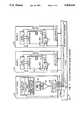
- FIG. 1A system 50 having one embodiment of the present invention is shown in FIG. 1.
- the utility boardcontains a 18.18 MHz TTL oscillator 54 of high stability. This oscillator drives the input of an F3038 gate 56, comprising an open-collector, high-output current buffer, which provides a common source of all (backplane) reference clock signals.
- the output of the F3038is pulled-up and source-terminated 58 with eight independent circuits (16 resistors).
- These eight clock leads 60 that leave the utility boardare load-terminated on each bus connected board with a 10 ⁇ series resistor and two Schottky diodes at the input of each PLL. Each of the eight outputs goes to a bus board slot through time-matched etch runs 62.
- the reference clock for the utility boardgoes out on the backplane and back in again with the appropriate amount of etch delay preferably equal to the clock delay for other boards 70A, 70B.
- the board clock distribution on each board 52, 70A, 70Bincludes PLL circuitry 72 and the distribution gate array (SCR) 74.
- the physical makeup of the PLL circuitis uniformly laid out on each bus board and in the same manner for all board types in the system.
- all clock paths on each circuit boardshould have their printed traces matched in length to within 1/4 inch.
- the clock fanout logicis part of the gate array 74 that is an ICS CMOS gate array referred to as the distribution portion of the gate array. Its outputs directly drive all the clock input pins on the board.
- the clock distribution portion's main input signalsare a 18.18 MHz clock and two delayed 18.18 MHz clocks from PLL 72.
- the delayed clocksare delayed by 5ns ( ⁇ 0.75ns) and 14.75 ns ( ⁇ 0.75ns).
- Other inputsinclude a power-on/reset signal and five control signals from other parts of the array.
- the clock portion 74 of the gate arrayfans out the clock to outputs whose pin-to-pin skew can be well controlled because the entire array is fabricated as a unit. Each of the outputs will drive 4 loads.
- the chipalso creates a 36.36 MHz signal that is in sync with the 18.18 MHz clock, discussed below.
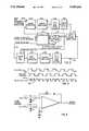
- the PLL circuitincludes a phase detector 102, error amplifier 104, low pass filter 106 (including an op-amp and associated resistors and capacitors), a voltage-controlled crystal oscillator 108 (VCXO), and a delay line 110.
- the phase-locked loop 72compensates for skew differences between distributors 74 on different bus boards 70, effectively reducing board-to-board clock skew, and also reducing the burden on the bus interface (BIF) to compensate for large skew between two clock sources.
- the VCXO 108is a 18.18 MHz VCXO with a high stability and a control voltage range of 0.5 to 4.5 V.
- the PLL circuitkeeps the rising edges of the R and V inputs to the phase detector 102 aligned.
- the VCXO 108creates a square wave with approximately a 60-40% duty cycle.
- the phase detector 102detects an offset between the output of the distributor 74 and the reference clock from the backplane and corrects the offset (aligns the outputs).
- the phase detector (comparator) 102comprises two ECL flip flops (10H131) and an ECL NOR gate (10H102).
- the Reference input to the phase comparatorcomes from the system backplane clock signal 60.
- the reference backplane signalis terminated, level shifted and clamped by input resistors and Schottky diodes to insure proper ECL logic levels and fast rise and fall times.
- the variable (V) input to be comparedis received from the output of the distributor 74 and is essentially a delayed version of the VCXO output. The delay resulting from distributor 74 varies from approximately 5ns to 10ns.
- the distributor 74 output signalis also level shifted and clamped to provide proper logic ECL levels and fast rise and fall time.
- the pulse output of the phase detectoris amplified, is filtered by an UA714TC op amp and associated discrete components.
- the offset voltage amplifier 104 of the (UA714TC)is trimmed so that when the entire phase locked loop is locked the error between the reference input and the locked inputs is less than 100ps.
- the third main blockis the delay line 110.
- the first outputis considered the main output, the other two outputs are referred to this main output.
- the main output signal on lead 11occurs 3.5ns ⁇ 2.0ns after the input changes relative to a fixed threshold. This initially is nulled out by the main loop of the PLL.
- the preferred parametersare: less than 4ns rise, fall time when driving one equivalent HC load; 5ns delay tap ( ⁇ 0.75ns) with respect to main output 111, rising edge to rising edge and falling edge to falling edge; and 14.75ns ( ⁇ 0.75ns, 1/4 cycle+1ns for rise time correction) with respect to main output 111, rising edge to rising edge and falling edge to falling edge.
- the other outputs of the distributor 74track very closely because circuits and paths inside the distributor 74 are very carefully matched.
- the PLLmaintains a lock while the distributor 74 on each bus board changes propagation delay due to changes in temperature and supply voltage. This produces less board-to-board clock skew than other methods that correct for the process variation only at power-up/boot time.
- the multiple frequency 36.36 MHz clock signalis generated by first passing the 18.18 MHz clock through a 14.75 ⁇ 0.75sns delay line 110. Both the normal 18.18 MHz and the delayed (154) 18.18 MHz enter the distributor 74 gate array. The two signals are EXOR'ed together inside the distributor to produce a 36.36 MHz clock signal (156) on lead 114. The normal 18.18 MHz is also passed through an EXOR gate with one of its inputs tied to ground. This will balance the delay and have the resulting 18.18 MHz and 36.36 MHz clock signals in tight sync. The skew of the delay line will only appear in the falling edge 152, FIG. 3. Since most of the system is rising edge triggered, the trailing edge skew is only important to the minimum pulse width issue.
- Duty cycle controlis important because any variation in duty cycle of the 18.18 MHz signal translates into cycle time asymmetry (adjacent cycle-to-cycle differences in period) of the 36.36 MHz clocks generated by the CMOS gate array comprising the distribution 74. Duty cycle control of the 18.18 MHz clock is necessary to insure that the cycle time of the 36.36 MHz clock is consistent (about 27.5ns).
- a symmetry loopalso shown in FIG. 2, includes a divide-by-two circuit 118, a duty cycle detector 120, an error amplifier 122, a low pass filter 124 and duty cycle control circuitry 112. This loop is used to insure a consistent cycle time of the 36.36 MHz clock and is achieved by modifying the duty cycle of the 18.18 MHz clock.
- the (FRUN) 36.36 MHz clockis divided by 2 in an ECL flip-flop 118.
- an error signalis generated by the duty cycle detector 120, which is amplified (122) and filtered (124).
- the rise and fall times of the VCXOare slowed to approximately 20ns by an RC network in the duty cycle control 112.
- the combination of the filtered error signal and the slowed down VCXO outputare combined resulting in shifting of the average DC level of the duty cycle control output signal (in response to the filter 124 output signal), causing the duty cycle of the delay line 110 output to be modified by the amount of the DC offset, as provided by variations in the slowed VCXO signal point which crosses a fixed threshold of the delay line 110.
- a differential buffer or comparatorhaving one input receiving the oscillator signal with slowed edges and the other input receiving the error voltage from filter 124 may be used. This creates a duty cycle which produces minimum cycle time variation in the 36.36 MHz clock.
- a typical gate array clock tree receiving the clock signals produced by the clock distributor 74will delay the clock signal by approximately 5ns in a fast array and 10ns in a slow array depending on manufacturing and other variables. This delay must be added in to the clock path before setup/hold (S/H) calculations can be done. This causes a problem when TTL MSI registers (not shown) are also used on the board and data is transferred between gate arrays and TTL MSI registers. With a common clock (clocking both the gate array and registers) the data is clocked into/out of the register 5-10ns before the same occurs inside of the gate array. To compensate for this effect, a delay line is added (lead 116) to the clocks that will clock the registers.
- the value of the delay lineis determined by a combination of the clock tree delay, the time it takes for the data to enter/exit the gate array and the setup/hold time of the register.
- the distributor 74provides clock outputs that are delayed by the correct amount.
- the arraycontains a fanout tree for the delayed clock signals (not shown) similar to the one used for the main 18.18 MHz clock.
- the range of the delay line selectioncan be calculated from the setup and hold time of the transfer to/from the register.
- the hold timedetermines the minimum delay line value and the setup time determines the maximum delay line value and the ideal value was calculated as 5ns.
- phase locked loop compensationis calculated as Per Floyd M. Gardner, Phaselock Techniques, Second Edition 1979 by John Wiley & Sons, Inc., "Loop Fundamentals," pp. 8-11, incorporated by reference.
- the loop error amplifieris a differential input variation of the one shown on page 11 of that reference. The equations are shown in the Appendix. ##EQU1##
Landscapes
- Engineering & Computer Science (AREA)
- Theoretical Computer Science (AREA)
- Physics & Mathematics (AREA)
- General Engineering & Computer Science (AREA)
- General Physics & Mathematics (AREA)
- Stabilization Of Oscillater, Synchronisation, Frequency Synthesizers (AREA)
- Manipulation Of Pulses (AREA)
- Dram (AREA)
Abstract
Description
Claims (9)
Priority Applications (4)
| Application Number | Priority Date | Filing Date | Title |
|---|---|---|---|
| US07/263,714US5008636A (en) | 1988-10-28 | 1988-10-28 | Apparatus for low skew system clock distribution and generation of 2X frequency clocks |
| EP89310613AEP0366326B1 (en) | 1988-10-28 | 1989-10-16 | Apparatus for low skew system clock distribution and generation of 2x frequency clocks |
| DE68926842TDE68926842T2 (en) | 1988-10-28 | 1989-10-16 | Device for a clock distribution system with low clock shift and generation of double-frequency clock signals |
| JP1281588AJPH02224104A (en) | 1988-10-28 | 1989-10-27 | Synchronization clock generator |
Applications Claiming Priority (1)
| Application Number | Priority Date | Filing Date | Title |
|---|---|---|---|
| US07/263,714US5008636A (en) | 1988-10-28 | 1988-10-28 | Apparatus for low skew system clock distribution and generation of 2X frequency clocks |
Publications (1)
| Publication Number | Publication Date |
|---|---|
| US5008636Atrue US5008636A (en) | 1991-04-16 |
Family
ID=23002950
Family Applications (1)
| Application Number | Title | Priority Date | Filing Date |
|---|---|---|---|
| US07/263,714Expired - LifetimeUS5008636A (en) | 1988-10-28 | 1988-10-28 | Apparatus for low skew system clock distribution and generation of 2X frequency clocks |
Country Status (4)
| Country | Link |
|---|---|
| US (1) | US5008636A (en) |
| EP (1) | EP0366326B1 (en) |
| JP (1) | JPH02224104A (en) |
| DE (1) | DE68926842T2 (en) |
Cited By (45)
| Publication number | Priority date | Publication date | Assignee | Title |
|---|---|---|---|---|
| US5355397A (en)* | 1992-09-24 | 1994-10-11 | Cray Research, Inc. | Clock start up stabilization for computer systems |
| US5442776A (en)* | 1994-06-30 | 1995-08-15 | International Business Machines, Corp. | Electronically tuneable computer clocking system and method of electronically tuning distribution lines of a computer clocking system |
| US5446867A (en)* | 1992-05-29 | 1995-08-29 | Intel Corporation | Microprocessor PLL clock circuit with selectable delayed feedback |
| US5451911A (en)* | 1994-04-07 | 1995-09-19 | Media Vision, Inc. | Timing generator |
| US5525914A (en)* | 1995-01-23 | 1996-06-11 | International Business Machines Corporation | CMOS driver circuit |
| US5539333A (en)* | 1995-01-23 | 1996-07-23 | International Business Machines Corporation | CMOS receiver circuit |
| US5548797A (en)* | 1994-10-03 | 1996-08-20 | International Business Machines Corporation | Digital clock pulse positioning circuit for delaying a signal input by a fist time duration and a second time duration to provide a positioned clock signal |
| US5568078A (en)* | 1994-12-30 | 1996-10-22 | Hyundai Electronics Industries Co., Ltd. | Clock delay compensating and duty controlling apparatus of a phase-locked loop |
| US5581699A (en)* | 1995-05-15 | 1996-12-03 | International Business Machines Corporation | System and method for testing a clock signal |
| GB2308250A (en)* | 1995-12-13 | 1997-06-18 | Altera Corp | Clock frequency multiplier using a delay line loop |
| US5764091A (en)* | 1995-01-25 | 1998-06-09 | Matsushita Electric Industrial Co., Ltd. | Method and system for clock-signal waveform correction |
| US5905769A (en)* | 1996-05-07 | 1999-05-18 | Silicon Image, Inc. | System and method for high-speed skew-insensitive multi-channel data transmission |
| US5963071A (en)* | 1998-01-22 | 1999-10-05 | Nanoamp Solutions, Inc. | Frequency doubler with adjustable duty cycle |
| US5982238A (en)* | 1995-08-08 | 1999-11-09 | Saab Dynamics Aktiebolag | Clock signal distribution and synchronization in a digital system |
| US6441666B1 (en) | 2000-07-20 | 2002-08-27 | Silicon Graphics, Inc. | System and method for generating clock signals |
| US6473440B1 (en)* | 1998-02-17 | 2002-10-29 | Samsung Electronics Co., Ltd. | Clock supplying apparatus for multiline transmission system |
| US6496552B2 (en)* | 1997-10-20 | 2002-12-17 | Fujitsu Limited | Timing circuit |
| US20030115542A1 (en)* | 2001-12-17 | 2003-06-19 | Sakyun Hwang | System and method for recovering and deserializing a high data rate bit stream |
| US20030147482A1 (en)* | 2002-02-06 | 2003-08-07 | Pasqualino Christopher R. | Single ended termination of clock for dual link DVI receiver |
| US20030149987A1 (en)* | 2002-02-06 | 2003-08-07 | Pasqualino Christopher R. | Synchronization of data links in a multiple link receiver |
| US20030152160A1 (en)* | 2002-02-12 | 2003-08-14 | Jeffrey Bauch | Dual link DVI transmitter serviced by single phase locked loop |
| US20040075462A1 (en)* | 2002-10-21 | 2004-04-22 | Rambus Inc. | Method and apparatus for digital duty cycle adjustment |
| US6750689B2 (en)* | 2001-03-29 | 2004-06-15 | Intel Corporation | Method and apparatus for correcting a clock duty cycle in a clock distribution network |
| US20050017457A1 (en)* | 2003-07-22 | 2005-01-27 | Brian Dubinsky | Inflatable balancing game |
| US20060256909A1 (en)* | 2005-05-10 | 2006-11-16 | Ftd Solutions Pte Ltd. | Single-VCO CDR for TMDS data at gigabit rate |
| US20080117172A1 (en)* | 2006-11-22 | 2008-05-22 | Fujitsu Component Limited | KVM switch and method of controlling the same |
| US20090128207A1 (en)* | 2007-11-21 | 2009-05-21 | Kun-Yung Chang | Clock Circuitry for Generating Multiple Clocks with Time-Multiplexed Duty Cycle Adjustment |
| US20100274548A1 (en)* | 2009-04-28 | 2010-10-28 | Du Nguyen | Clock Approximation for Hardware Simulation |
| US8977211B1 (en)* | 2012-02-29 | 2015-03-10 | Marvell International Ltd. | Systems and methods for calibrating harmonic rejection in switching mixers |
| US10425070B2 (en) | 2015-06-22 | 2019-09-24 | Gsi Technology, Inc. | Systems and methods involving lock-loop circuits, clock signal alignment, phase-averaging feedback clock circuitry |
| US10521229B2 (en) | 2016-12-06 | 2019-12-31 | Gsi Technology, Inc. | Computational memory cell and processing array device using memory cells |
| US10659058B1 (en)* | 2015-06-26 | 2020-05-19 | Gsi Technology, Inc. | Systems and methods involving lock loop circuits, distributed duty cycle correction loop circuitry |
| US10770133B1 (en) | 2016-12-06 | 2020-09-08 | Gsi Technology, Inc. | Read and write data processing circuits and methods associated with computational memory cells that provides write inhibits and read bit line pre-charge inhibits |
| US10777262B1 (en) | 2016-12-06 | 2020-09-15 | Gsi Technology, Inc. | Read data processing circuits and methods associated memory cells |
| US10847212B1 (en) | 2016-12-06 | 2020-11-24 | Gsi Technology, Inc. | Read and write data processing circuits and methods associated with computational memory cells using two read multiplexers |
| US10847213B1 (en) | 2016-12-06 | 2020-11-24 | Gsi Technology, Inc. | Write data processing circuits and methods associated with computational memory cells |
| US10854284B1 (en) | 2016-12-06 | 2020-12-01 | Gsi Technology, Inc. | Computational memory cell and processing array device with ratioless write port |
| US10860320B1 (en) | 2016-12-06 | 2020-12-08 | Gsi Technology, Inc. | Orthogonal data transposition system and method during data transfers to/from a processing array |
| US10877731B1 (en) | 2019-06-18 | 2020-12-29 | Gsi Technology, Inc. | Processing array device that performs one cycle full adder operation and bit line read/write logic features |
| US10891076B1 (en) | 2016-12-06 | 2021-01-12 | Gsi Technology, Inc. | Results processing circuits and methods associated with computational memory cells |
| US10930341B1 (en) | 2019-06-18 | 2021-02-23 | Gsi Technology, Inc. | Processing array device that performs one cycle full adder operation and bit line read/write logic features |
| US10943648B1 (en) | 2016-12-06 | 2021-03-09 | Gsi Technology, Inc. | Ultra low VDD memory cell with ratioless write port |
| US10958272B2 (en) | 2019-06-18 | 2021-03-23 | Gsi Technology, Inc. | Computational memory cell and processing array device using complementary exclusive or memory cells |
| US10998040B2 (en) | 2016-12-06 | 2021-05-04 | Gsi Technology, Inc. | Computational memory cell and processing array device using the memory cells for XOR and XNOR computations |
| US11227653B1 (en) | 2016-12-06 | 2022-01-18 | Gsi Technology, Inc. | Storage array circuits and methods for computational memory cells |
Families Citing this family (19)
| Publication number | Priority date | Publication date | Assignee | Title |
|---|---|---|---|---|
| FR2666424B1 (en)* | 1990-08-30 | 1992-11-06 | Bull Sa | METHOD AND DEVICE FOR ADJUSTING CLOCK SIGNALS IN A SYNCHRONOUS SYSTEM. |
| JPH0817489B2 (en)* | 1990-10-01 | 1996-02-21 | 株式会社セガ・エンタープライゼス | A method of synchronizing multiple devices in an electronic game system |
| US5842029A (en)* | 1991-10-17 | 1998-11-24 | Intel Corporation | Method and apparatus for powering down an integrated circuit transparently and its phase locked loop |
| US5935253A (en)* | 1991-10-17 | 1999-08-10 | Intel Corporation | Method and apparatus for powering down an integrated circuit having a core that operates at a speed greater than the bus frequency |
| GB2260631B (en)* | 1991-10-17 | 1995-06-28 | Intel Corp | Microprocessor 2X core design |
| US5473767A (en)* | 1992-11-03 | 1995-12-05 | Intel Corporation | Method and apparatus for asynchronously stopping the clock in a processor |
| EP0596657A3 (en)* | 1992-11-05 | 1994-12-07 | American Telephone & Telegraph | Normalization of apparent propagation delay. |
| DE4239329C1 (en)* | 1992-11-23 | 1993-12-23 | Siemens Nixdorf Inf Syst | Circuit arrangement for a comparison of individual clock signals for the clock supply of individual components of a data processing system and method for controlling or monitoring a ring circuit contained in the circuit arrangement |
| US6130475A (en)* | 1993-12-07 | 2000-10-10 | International Business Machines Corporation | Clock distribution system for synchronous circuit assemblies |
| JP3048495B2 (en)* | 1994-01-07 | 2000-06-05 | 沖電気工業株式会社 | Clock circuit |
| US5428317A (en)* | 1994-09-06 | 1995-06-27 | Motorola, Inc. | Phase locked loop with low power feedback path and method of operation |
| US5675620A (en)* | 1994-10-26 | 1997-10-07 | At&T Global Information Solutions Company | High-frequency phase locked loop circuit |
| SE506739C2 (en) | 1995-09-29 | 1998-02-09 | Ericsson Telefon Ab L M | Operation and maintenance of clock distribution networks with redundancy |
| SE504920C2 (en) | 1995-09-29 | 1997-05-26 | Ericsson Telefon Ab L M | Method and system for redundant clock distribution to telecommunications equipment in which switching of selected clock signal among the incoming clock signals is constantly taking place |
| US5802132A (en) | 1995-12-29 | 1998-09-01 | Intel Corporation | Apparatus for generating bus clock signals with a 1/N characteristic in a 2/N mode clocking scheme |
| US5777498A (en) | 1996-12-02 | 1998-07-07 | Sgs-Thomson Microelectronics, Inc. | Data compensation/resynchronization circuit for phase lock loops |
| US6188286B1 (en)* | 1999-03-30 | 2001-02-13 | Infineon Technologies North America Corp. | Method and system for synchronizing multiple subsystems using one voltage-controlled oscillator |
| US8519763B2 (en)* | 2010-06-11 | 2013-08-27 | Altera Corporation | Integrated circuits with dual-edge clocking |
| EP3602775A2 (en) | 2017-03-20 | 2020-02-05 | Blue Danube Systems, Inc. | Precision high frequency phase adders |
Citations (8)
| Publication number | Priority date | Publication date | Assignee | Title |
|---|---|---|---|---|
| US3493884A (en)* | 1968-06-03 | 1970-02-03 | Us Army | Phase shift system incorporating an integrator |
| US4021740A (en)* | 1976-01-30 | 1977-05-03 | Communications Satellite Corporation (Comsat) | Sinewave clock driver with adjustable delay |
| US4185245A (en)* | 1978-05-15 | 1980-01-22 | International Telephone And Telegraph Corporation | Fault-tolerant clock signal distribution arrangement |
| GB2120878A (en)* | 1982-05-07 | 1983-12-07 | Philips Electronic Associated | Phase-locked-loops |
| EP0103404A2 (en)* | 1982-08-30 | 1984-03-21 | Xerox Corporation | Self-calibrated clock and timing signal generator |
| US4439689A (en)* | 1980-12-29 | 1984-03-27 | Henri Chazenfus | Circuit for the control of the cyclic ratio of a periodic pulse signal and device multiplying by 2n of a pulse signal frequency incorporating said control circuit |
| US4754166A (en)* | 1982-04-21 | 1988-06-28 | Tokyo Shibaura Denki Kabushiki Kaisha | Reset circuit for integrated injection logic |
| EP0302262A2 (en)* | 1987-08-07 | 1989-02-08 | Tektronix, Inc. | High speed partioned reduced instruction set computer |
Family Cites Families (1)
| Publication number | Priority date | Publication date | Assignee | Title |
|---|---|---|---|---|
| US3588713A (en)* | 1968-09-04 | 1971-06-28 | Bendix Corp | Multiplier circuit |
- 1988
- 1988-10-28USUS07/263,714patent/US5008636A/ennot_activeExpired - Lifetime
- 1989
- 1989-10-16DEDE68926842Tpatent/DE68926842T2/ennot_activeExpired - Fee Related
- 1989-10-16EPEP89310613Apatent/EP0366326B1/ennot_activeExpired - Lifetime
- 1989-10-27JPJP1281588Apatent/JPH02224104A/enactivePending
Patent Citations (8)
| Publication number | Priority date | Publication date | Assignee | Title |
|---|---|---|---|---|
| US3493884A (en)* | 1968-06-03 | 1970-02-03 | Us Army | Phase shift system incorporating an integrator |
| US4021740A (en)* | 1976-01-30 | 1977-05-03 | Communications Satellite Corporation (Comsat) | Sinewave clock driver with adjustable delay |
| US4185245A (en)* | 1978-05-15 | 1980-01-22 | International Telephone And Telegraph Corporation | Fault-tolerant clock signal distribution arrangement |
| US4439689A (en)* | 1980-12-29 | 1984-03-27 | Henri Chazenfus | Circuit for the control of the cyclic ratio of a periodic pulse signal and device multiplying by 2n of a pulse signal frequency incorporating said control circuit |
| US4754166A (en)* | 1982-04-21 | 1988-06-28 | Tokyo Shibaura Denki Kabushiki Kaisha | Reset circuit for integrated injection logic |
| GB2120878A (en)* | 1982-05-07 | 1983-12-07 | Philips Electronic Associated | Phase-locked-loops |
| EP0103404A2 (en)* | 1982-08-30 | 1984-03-21 | Xerox Corporation | Self-calibrated clock and timing signal generator |
| EP0302262A2 (en)* | 1987-08-07 | 1989-02-08 | Tektronix, Inc. | High speed partioned reduced instruction set computer |
Non-Patent Citations (2)
| Title |
|---|
| IEEE Design & Test of Computers, vol. 5, No. 5, Oct. 1988, pp. 9 27: Clock System Design , Wagner.* |
| IEEE Design & Test of Computers, vol. 5, No. 5, Oct. 1988, pp. 9-27: "Clock System Design", Wagner. |
Cited By (73)
| Publication number | Priority date | Publication date | Assignee | Title |
|---|---|---|---|---|
| US5446867A (en)* | 1992-05-29 | 1995-08-29 | Intel Corporation | Microprocessor PLL clock circuit with selectable delayed feedback |
| US5355397A (en)* | 1992-09-24 | 1994-10-11 | Cray Research, Inc. | Clock start up stabilization for computer systems |
| US5451911A (en)* | 1994-04-07 | 1995-09-19 | Media Vision, Inc. | Timing generator |
| WO1995028032A1 (en)* | 1994-04-07 | 1995-10-19 | Media Vision, Inc. | Timing generator |
| US5442776A (en)* | 1994-06-30 | 1995-08-15 | International Business Machines, Corp. | Electronically tuneable computer clocking system and method of electronically tuning distribution lines of a computer clocking system |
| US5548797A (en)* | 1994-10-03 | 1996-08-20 | International Business Machines Corporation | Digital clock pulse positioning circuit for delaying a signal input by a fist time duration and a second time duration to provide a positioned clock signal |
| US5568078A (en)* | 1994-12-30 | 1996-10-22 | Hyundai Electronics Industries Co., Ltd. | Clock delay compensating and duty controlling apparatus of a phase-locked loop |
| US5539333A (en)* | 1995-01-23 | 1996-07-23 | International Business Machines Corporation | CMOS receiver circuit |
| US5525914A (en)* | 1995-01-23 | 1996-06-11 | International Business Machines Corporation | CMOS driver circuit |
| US5764091A (en)* | 1995-01-25 | 1998-06-09 | Matsushita Electric Industrial Co., Ltd. | Method and system for clock-signal waveform correction |
| US5581699A (en)* | 1995-05-15 | 1996-12-03 | International Business Machines Corporation | System and method for testing a clock signal |
| US6311295B1 (en) | 1995-05-15 | 2001-10-30 | International Business Machines Corporation | System and method for testing a clock signal |
| US5982238A (en)* | 1995-08-08 | 1999-11-09 | Saab Dynamics Aktiebolag | Clock signal distribution and synchronization in a digital system |
| GB2308250A (en)* | 1995-12-13 | 1997-06-18 | Altera Corp | Clock frequency multiplier using a delay line loop |
| US5905769A (en)* | 1996-05-07 | 1999-05-18 | Silicon Image, Inc. | System and method for high-speed skew-insensitive multi-channel data transmission |
| US6496552B2 (en)* | 1997-10-20 | 2002-12-17 | Fujitsu Limited | Timing circuit |
| US6850581B2 (en) | 1997-10-20 | 2005-02-01 | Fujitsu Limited | Timing circuit |
| US5963071A (en)* | 1998-01-22 | 1999-10-05 | Nanoamp Solutions, Inc. | Frequency doubler with adjustable duty cycle |
| US6473440B1 (en)* | 1998-02-17 | 2002-10-29 | Samsung Electronics Co., Ltd. | Clock supplying apparatus for multiline transmission system |
| US6441666B1 (en) | 2000-07-20 | 2002-08-27 | Silicon Graphics, Inc. | System and method for generating clock signals |
| US20040217792A1 (en)* | 2001-03-29 | 2004-11-04 | Fletcher Thomas D | Smart buffer circuit to match a delay over a range of loads |
| US7009437B2 (en) | 2001-03-29 | 2006-03-07 | Intel Corporation | Smart buffer circuit to match a delay over a range of loads |
| US6750689B2 (en)* | 2001-03-29 | 2004-06-15 | Intel Corporation | Method and apparatus for correcting a clock duty cycle in a clock distribution network |
| US20030115542A1 (en)* | 2001-12-17 | 2003-06-19 | Sakyun Hwang | System and method for recovering and deserializing a high data rate bit stream |
| US7092466B2 (en) | 2001-12-17 | 2006-08-15 | Broadcom Corporation | System and method for recovering and deserializing a high data rate bit stream |
| US20080089456A1 (en)* | 2002-02-06 | 2008-04-17 | Broadcom Corporation | Synchronization of Data Links in a Multiple Link Receiver |
| US7308059B2 (en) | 2002-02-06 | 2007-12-11 | Broadcom Corporation | Synchronization of data links in a multiple link receiver |
| US7450676B2 (en)* | 2002-02-06 | 2008-11-11 | Broadcom Corporation | Synchronization of data links in a multiple link receiver |
| US20030147482A1 (en)* | 2002-02-06 | 2003-08-07 | Pasqualino Christopher R. | Single ended termination of clock for dual link DVI receiver |
| US7099416B2 (en) | 2002-02-06 | 2006-08-29 | Broadcom Corporation | Single ended termination of clock for dual link DVI receiver |
| US20030149987A1 (en)* | 2002-02-06 | 2003-08-07 | Pasqualino Christopher R. | Synchronization of data links in a multiple link receiver |
| US7254183B2 (en) | 2002-02-12 | 2007-08-07 | Broadcom Corporation | Dual link DVI transmitter serviced by single phase locked loop |
| US7120203B2 (en) | 2002-02-12 | 2006-10-10 | Broadcom Corporation | Dual link DVI transmitter serviced by single Phase Locked Loop |
| US20030152160A1 (en)* | 2002-02-12 | 2003-08-14 | Jeffrey Bauch | Dual link DVI transmitter serviced by single phase locked loop |
| US20070002965A1 (en)* | 2002-02-12 | 2007-01-04 | Broadcom Corporation, A California Corporation | Dual link DVI transmitter serviced by single phase locked loop |
| US20040075462A1 (en)* | 2002-10-21 | 2004-04-22 | Rambus Inc. | Method and apparatus for digital duty cycle adjustment |
| US6967514B2 (en)* | 2002-10-21 | 2005-11-22 | Rambus, Inc. | Method and apparatus for digital duty cycle adjustment |
| US20050017457A1 (en)* | 2003-07-22 | 2005-01-27 | Brian Dubinsky | Inflatable balancing game |
| US20060256909A1 (en)* | 2005-05-10 | 2006-11-16 | Ftd Solutions Pte Ltd. | Single-VCO CDR for TMDS data at gigabit rate |
| US7492849B2 (en)* | 2005-05-10 | 2009-02-17 | Ftd Solutions Pte., Ltd. | Single-VCO CDR for TMDS data at gigabit rate |
| US8169407B2 (en)* | 2006-11-22 | 2012-05-01 | Fujitsu Component Limited | KVM switch and method of controlling the same |
| US20080117172A1 (en)* | 2006-11-22 | 2008-05-22 | Fujitsu Component Limited | KVM switch and method of controlling the same |
| US20090128207A1 (en)* | 2007-11-21 | 2009-05-21 | Kun-Yung Chang | Clock Circuitry for Generating Multiple Clocks with Time-Multiplexed Duty Cycle Adjustment |
| US7839194B2 (en) | 2007-11-21 | 2010-11-23 | Rambus Inc. | Clock circuitry for generating multiple clocks with time-multiplexed duty cycle adjustment |
| US20100274548A1 (en)* | 2009-04-28 | 2010-10-28 | Du Nguyen | Clock Approximation for Hardware Simulation |
| US8977211B1 (en)* | 2012-02-29 | 2015-03-10 | Marvell International Ltd. | Systems and methods for calibrating harmonic rejection in switching mixers |
| US9236960B1 (en) | 2012-02-29 | 2016-01-12 | Marvell International Ltd. | Calibration circuit and methods for calibrating harmonics in a mixer |
| US10425070B2 (en) | 2015-06-22 | 2019-09-24 | Gsi Technology, Inc. | Systems and methods involving lock-loop circuits, clock signal alignment, phase-averaging feedback clock circuitry |
| US10659058B1 (en)* | 2015-06-26 | 2020-05-19 | Gsi Technology, Inc. | Systems and methods involving lock loop circuits, distributed duty cycle correction loop circuitry |
| US10521229B2 (en) | 2016-12-06 | 2019-12-31 | Gsi Technology, Inc. | Computational memory cell and processing array device using memory cells |
| US11150903B2 (en) | 2016-12-06 | 2021-10-19 | Gsi Technology, Inc. | Computational memory cell and processing array device using memory cells |
| US10770133B1 (en) | 2016-12-06 | 2020-09-08 | Gsi Technology, Inc. | Read and write data processing circuits and methods associated with computational memory cells that provides write inhibits and read bit line pre-charge inhibits |
| US10777262B1 (en) | 2016-12-06 | 2020-09-15 | Gsi Technology, Inc. | Read data processing circuits and methods associated memory cells |
| US10847212B1 (en) | 2016-12-06 | 2020-11-24 | Gsi Technology, Inc. | Read and write data processing circuits and methods associated with computational memory cells using two read multiplexers |
| US10847213B1 (en) | 2016-12-06 | 2020-11-24 | Gsi Technology, Inc. | Write data processing circuits and methods associated with computational memory cells |
| US10854284B1 (en) | 2016-12-06 | 2020-12-01 | Gsi Technology, Inc. | Computational memory cell and processing array device with ratioless write port |
| US10860318B2 (en) | 2016-12-06 | 2020-12-08 | Gsi Technology, Inc. | Computational memory cell and processing array device using memory cells |
| US10860320B1 (en) | 2016-12-06 | 2020-12-08 | Gsi Technology, Inc. | Orthogonal data transposition system and method during data transfers to/from a processing array |
| US11763881B2 (en) | 2016-12-06 | 2023-09-19 | Gsi Technology, Inc. | Computational memory cell and processing array device using the memory cells for XOR and XNOR computations |
| US10891076B1 (en) | 2016-12-06 | 2021-01-12 | Gsi Technology, Inc. | Results processing circuits and methods associated with computational memory cells |
| US11409528B2 (en) | 2016-12-06 | 2022-08-09 | Gsi Technology, Inc. | Orthogonal data transposition system and method during data transfers to/from a processing array |
| US10943648B1 (en) | 2016-12-06 | 2021-03-09 | Gsi Technology, Inc. | Ultra low VDD memory cell with ratioless write port |
| US11257540B2 (en) | 2016-12-06 | 2022-02-22 | Gsi Technology, Inc. | Write data processing methods associated with computational memory cells |
| US10998040B2 (en) | 2016-12-06 | 2021-05-04 | Gsi Technology, Inc. | Computational memory cell and processing array device using the memory cells for XOR and XNOR computations |
| US11094374B1 (en) | 2016-12-06 | 2021-08-17 | Gsi Technology, Inc. | Write data processing circuits and methods associated with computational memory cells |
| US10725777B2 (en) | 2016-12-06 | 2020-07-28 | Gsi Technology, Inc. | Computational memory cell and processing array device using memory cells |
| US11194519B2 (en) | 2016-12-06 | 2021-12-07 | Gsi Technology, Inc. | Results processing circuits and methods associated with computational memory cells |
| US11227653B1 (en) | 2016-12-06 | 2022-01-18 | Gsi Technology, Inc. | Storage array circuits and methods for computational memory cells |
| US11205476B1 (en) | 2016-12-06 | 2021-12-21 | Gsi Technology, Inc. | Read data processing circuits and methods associated with computational memory cells |
| US11194548B2 (en) | 2019-06-18 | 2021-12-07 | Gsi Technology, Inc. | Processing array device that performs one cycle full adder operation and bit line read/write logic features |
| US10958272B2 (en) | 2019-06-18 | 2021-03-23 | Gsi Technology, Inc. | Computational memory cell and processing array device using complementary exclusive or memory cells |
| US10930341B1 (en) | 2019-06-18 | 2021-02-23 | Gsi Technology, Inc. | Processing array device that performs one cycle full adder operation and bit line read/write logic features |
| US10877731B1 (en) | 2019-06-18 | 2020-12-29 | Gsi Technology, Inc. | Processing array device that performs one cycle full adder operation and bit line read/write logic features |
Also Published As
| Publication number | Publication date |
|---|---|
| EP0366326B1 (en) | 1996-07-17 |
| EP0366326A2 (en) | 1990-05-02 |
| DE68926842T2 (en) | 1996-11-28 |
| DE68926842D1 (en) | 1996-08-22 |
| EP0366326A3 (en) | 1990-12-05 |
| JPH02224104A (en) | 1990-09-06 |
Similar Documents
| Publication | Publication Date | Title |
|---|---|---|
| US5008636A (en) | Apparatus for low skew system clock distribution and generation of 2X frequency clocks | |
| US7423462B2 (en) | Clock capture in clock synchronization circuitry | |
| US7941685B2 (en) | Delay locked loop for an FPGA architecture | |
| US6658043B2 (en) | Method and apparatus for providing multiple spread spectrum clock generator circuits with overlapping output frequencies | |
| US5771264A (en) | Digital delay lock loop for clock signal frequency multiplication | |
| US5355037A (en) | High performance digital phase locked loop | |
| US5406590A (en) | Method of and apparatus for correcting edge placement errors in multiplying phase locked loop circuits | |
| US8269544B2 (en) | Power-supply noise suppression using a frequency-locked loop | |
| US5712583A (en) | Clock phase alignment using frequency comparison | |
| JPH1168559A (en) | Phase-locked loop circuit | |
| USRE38045E1 (en) | Data compensation/resynchronization circuit for phase lock loops | |
| US5666079A (en) | Binary relative delay line | |
| US7088172B1 (en) | Configurable voltage bias circuit for controlling buffer delays | |
| US20040193931A1 (en) | System and method for transferring data from a first clock domain to a second clock domain | |
| US6967536B2 (en) | Phase-locked loop circuit reducing steady state phase error | |
| US7490257B2 (en) | Clock distributor for use in semiconductor logics for generating clock signals when enabled and a method therefor | |
| JP3786540B2 (en) | Timing control circuit device | |
| US7171575B1 (en) | Delay locked loop for and FPGA architecture | |
| JP3896217B2 (en) | Timing control circuit device and clock distribution system | |
| JPS5839325A (en) | Timing pulse generating circuit | |
| JPH06188701A (en) | Ic-implemented clock pulse supply circuit for synchronous logic circuit |
Legal Events
| Date | Code | Title | Description |
|---|---|---|---|
| AS | Assignment | Owner name:APOLLO COMPUTER INC., MASSACHUSETTS Free format text:ASSIGNMENT OF ASSIGNORS INTEREST.;ASSIGNOR:HOGAN, THOMAS;REEL/FRAME:005150/0631 Effective date:19881128 Owner name:APOLLO COMPUTER INC., MASSACHUSETTS Free format text:ASSIGNMENT OF ASSIGNORS INTEREST.;ASSIGNORS:MARKINSON, SCOTT;SCHUSTER, MICHAEL;REEL/FRAME:005150/0627;SIGNING DATES FROM 19890420 TO 19890515 | |
| STCF | Information on status: patent grant | Free format text:PATENTED CASE | |
| AS | Assignment | Owner name:HEWLETT-PACKARD COMPANY A CA CORPORATION, CALIF Free format text:ASSIGNMENT OF ASSIGNORS INTEREST.;ASSIGNOR:APOLLO COMPUTER INCORPORATED;REEL/FRAME:005697/0780 Effective date:19910422 | |
| CC | Certificate of correction | ||
| FEPP | Fee payment procedure | Free format text:PAYOR NUMBER ASSIGNED (ORIGINAL EVENT CODE: ASPN); ENTITY STATUS OF PATENT OWNER: LARGE ENTITY | |
| FPAY | Fee payment | Year of fee payment:4 | |
| FPAY | Fee payment | Year of fee payment:8 | |
| AS | Assignment | Owner name:HEWLETT-PACKARD COMPANY, COLORADO Free format text:MERGER;ASSIGNOR:HEWLETT-PACKARD COMPANY;REEL/FRAME:011523/0469 Effective date:19980520 | |
| FPAY | Fee payment | Year of fee payment:12 | |
| REMI | Maintenance fee reminder mailed |