US5006476A - Transistor manufacturing process using three-step base doping - Google Patents
Transistor manufacturing process using three-step base dopingDownload PDFInfo
- Publication number
- US5006476A US5006476AUS07/440,456US44045689AUS5006476AUS 5006476 AUS5006476 AUS 5006476AUS 44045689 AUS44045689 AUS 44045689AUS 5006476 AUS5006476 AUS 5006476A
- Authority
- US
- United States
- Prior art keywords
- conductivity type
- zone
- layer
- region
- patterned
- Prior art date
- Legal status (The legal status is an assumption and is not a legal conclusion. Google has not performed a legal analysis and makes no representation as to the accuracy of the status listed.)
- Expired - Lifetime
Links
Images


Classifications
- H—ELECTRICITY
- H10—SEMICONDUCTOR DEVICES; ELECTRIC SOLID-STATE DEVICES NOT OTHERWISE PROVIDED FOR
- H10D—INORGANIC ELECTRIC SEMICONDUCTOR DEVICES
- H10D10/00—Bipolar junction transistors [BJT]
- H10D10/01—Manufacture or treatment
- H10D10/051—Manufacture or treatment of vertical BJTs
- H—ELECTRICITY
- H01—ELECTRIC ELEMENTS
- H01L—SEMICONDUCTOR DEVICES NOT COVERED BY CLASS H10
- H01L21/00—Processes or apparatus adapted for the manufacture or treatment of semiconductor or solid state devices or of parts thereof
- H01L21/02—Manufacture or treatment of semiconductor devices or of parts thereof
- H01L21/04—Manufacture or treatment of semiconductor devices or of parts thereof the devices having potential barriers, e.g. a PN junction, depletion layer or carrier concentration layer
- H01L21/18—Manufacture or treatment of semiconductor devices or of parts thereof the devices having potential barriers, e.g. a PN junction, depletion layer or carrier concentration layer the devices having semiconductor bodies comprising elements of Group IV of the Periodic Table or AIIIBV compounds with or without impurities, e.g. doping materials
- H01L21/28—Manufacture of electrodes on semiconductor bodies using processes or apparatus not provided for in groups H01L21/20 - H01L21/268
- H01L21/283—Deposition of conductive or insulating materials for electrodes conducting electric current
- H01L21/285—Deposition of conductive or insulating materials for electrodes conducting electric current from a gas or vapour, e.g. condensation
- H01L21/28506—Deposition of conductive or insulating materials for electrodes conducting electric current from a gas or vapour, e.g. condensation of conductive layers
- H01L21/28512—Deposition of conductive or insulating materials for electrodes conducting electric current from a gas or vapour, e.g. condensation of conductive layers on semiconductor bodies comprising elements of Group IV of the Periodic Table
- H01L21/28525—Deposition of conductive or insulating materials for electrodes conducting electric current from a gas or vapour, e.g. condensation of conductive layers on semiconductor bodies comprising elements of Group IV of the Periodic Table the conductive layers comprising semiconducting material
- H—ELECTRICITY
- H10—SEMICONDUCTOR DEVICES; ELECTRIC SOLID-STATE DEVICES NOT OTHERWISE PROVIDED FOR
- H10D—INORGANIC ELECTRIC SEMICONDUCTOR DEVICES
- H10D30/00—Field-effect transistors [FET]
- H10D30/01—Manufacture or treatment
- H10D30/021—Manufacture or treatment of FETs having insulated gates [IGFET]
- H10D30/0223—Manufacture or treatment of FETs having insulated gates [IGFET] having source and drain regions or source and drain extensions self-aligned to sides of the gate
- H10D30/0227—Manufacture or treatment of FETs having insulated gates [IGFET] having source and drain regions or source and drain extensions self-aligned to sides of the gate having both lightly-doped source and drain extensions and source and drain regions self-aligned to the sides of the gate, e.g. lightly-doped drain [LDD] MOSFET or double-diffused drain [DDD] MOSFET
- H—ELECTRICITY
- H10—SEMICONDUCTOR DEVICES; ELECTRIC SOLID-STATE DEVICES NOT OTHERWISE PROVIDED FOR
- H10D—INORGANIC ELECTRIC SEMICONDUCTOR DEVICES
- H10D62/00—Semiconductor bodies, or regions thereof, of devices having potential barriers
- H10D62/10—Shapes, relative sizes or dispositions of the regions of the semiconductor bodies; Shapes of the semiconductor bodies
- H10D62/17—Semiconductor regions connected to electrodes not carrying current to be rectified, amplified or switched, e.g. channel regions
- H10D62/177—Base regions of bipolar transistors, e.g. BJTs or IGBTs
- H—ELECTRICITY
- H10—SEMICONDUCTOR DEVICES; ELECTRIC SOLID-STATE DEVICES NOT OTHERWISE PROVIDED FOR
- H10D—INORGANIC ELECTRIC SEMICONDUCTOR DEVICES
- H10D84/00—Integrated devices formed in or on semiconductor substrates that comprise only semiconducting layers, e.g. on Si wafers or on GaAs-on-Si wafers
- H10D84/01—Manufacture or treatment
- H10D84/0107—Integrating at least one component covered by H10D12/00 or H10D30/00 with at least one component covered by H10D8/00, H10D10/00 or H10D18/00, e.g. integrating IGFETs with BJTs
- H10D84/0109—Integrating at least one component covered by H10D12/00 or H10D30/00 with at least one component covered by H10D8/00, H10D10/00 or H10D18/00, e.g. integrating IGFETs with BJTs the at least one component covered by H10D12/00 or H10D30/00 being a MOS device
- H—ELECTRICITY
- H10—SEMICONDUCTOR DEVICES; ELECTRIC SOLID-STATE DEVICES NOT OTHERWISE PROVIDED FOR
- H10D—INORGANIC ELECTRIC SEMICONDUCTOR DEVICES
- H10D84/00—Integrated devices formed in or on semiconductor substrates that comprise only semiconducting layers, e.g. on Si wafers or on GaAs-on-Si wafers
- H10D84/01—Manufacture or treatment
- H10D84/02—Manufacture or treatment characterised by using material-based technologies
- H10D84/03—Manufacture or treatment characterised by using material-based technologies using Group IV technology, e.g. silicon technology or silicon-carbide [SiC] technology
- H10D84/038—Manufacture or treatment characterised by using material-based technologies using Group IV technology, e.g. silicon technology or silicon-carbide [SiC] technology using silicon technology, e.g. SiGe
- Y—GENERAL TAGGING OF NEW TECHNOLOGICAL DEVELOPMENTS; GENERAL TAGGING OF CROSS-SECTIONAL TECHNOLOGIES SPANNING OVER SEVERAL SECTIONS OF THE IPC; TECHNICAL SUBJECTS COVERED BY FORMER USPC CROSS-REFERENCE ART COLLECTIONS [XRACs] AND DIGESTS
- Y10—TECHNICAL SUBJECTS COVERED BY FORMER USPC
- Y10S—TECHNICAL SUBJECTS COVERED BY FORMER USPC CROSS-REFERENCE ART COLLECTIONS [XRACs] AND DIGESTS
- Y10S148/00—Metal treatment
- Y10S148/009—Bi-MOS
- Y—GENERAL TAGGING OF NEW TECHNOLOGICAL DEVELOPMENTS; GENERAL TAGGING OF CROSS-SECTIONAL TECHNOLOGIES SPANNING OVER SEVERAL SECTIONS OF THE IPC; TECHNICAL SUBJECTS COVERED BY FORMER USPC CROSS-REFERENCE ART COLLECTIONS [XRACs] AND DIGESTS
- Y10—TECHNICAL SUBJECTS COVERED BY FORMER USPC
- Y10S—TECHNICAL SUBJECTS COVERED BY FORMER USPC CROSS-REFERENCE ART COLLECTIONS [XRACs] AND DIGESTS
- Y10S148/00—Metal treatment
- Y10S148/124—Polycrystalline emitter
Definitions
- This inventionrelates to methods of fabricating transistors.
- a bipolar transistorconsisting of an emitter, a base, and a collector is typically created in a vertical arrangement from a monocrystalline semiconductor body having a pair of generally flat opposing surfaces.
- the emitteris located in the semiconductor material along one of the two surfaces, referred to here (for convenience) as the upper surface.
- the baseis composed of an intrinsic base portion and one or two extrinsic base portions.
- the intrinsic base (portion)lies directly under the emitter.
- Each extrinsic base (portion)consists of a connection zone and a heavily doped contact zone which reaches the upper surface at a location laterally separated from the emitter.
- the connection zoneprovides an electrical path between the intrinsic base and the contact zone.
- the main part of the collectoris situated below the intrinsic base so that the emitter-to-collector current generally flows in the vertical direction.
- the collectoralso includes at least one heavily doped contact zone. A set of overlying electrical contacts to the emitter and to the various contact zones complete the transistor.
- the emitter and the intrinsic baseneed to be quite shallow. Also, the emitter needs to be close to the base contact zone(s), but not so close as to create a significant risk of an electrical short between the contacts.
- These objectivescan be achieved with a manufacturing process in which the emitter is formed in a self-aligned manner by impurity outdiffusion from a doped non-monocrystalline semiconductor layer that later serves as the emitter contact. Electrically insulating spacers along the sides of the non-monocrystalline layer are used in creating the base contact zone(s) in a self-aligned manner. The sidewall spacers also help separate the base contact zone(s) from the non-monocrystalline layer.
- Iwasakidiscloses how an NPN transistor is manufactured according to one version of the foregoing process.
- Iwasakimanufactures a P-channel insulated-gate field-effect transistor (FET) in conjunction with the NPN device.
- the two transistorsare built from a monocrystalline silicon (sometimes simply "monosilicon") body that contains a pair of major N-type regions, referred to here as the first and second regions, spaced apart from each other along the upper surface of the body.
- the NPN transistoris formed from the first region.
- the second regionis used for the P-channel FET.
- Iwasakiprovides an oxide layer along the upper surfaces of the two N-type regions. Boron is ion implanted into the first region through the oxide layer to convert a surface-adjoining portion into a primary P-type zone. Part of the P-type zone later serves as both the intrinsic base portion and the base connection zone. An emitter diffusion window is etched through the oxide down to the P-type zone.
- the first and second patterned layersserve respectively as the emitter contact for the NPN transistor and the gate electrode for the FET.
- Boronis ion implanted into the major regions through selected parts of their upper surfaces to establish a surface-adjoining portion of the first region as a heavily doped P-type base contact zone for the NPN device and to establish a pair of surface-adjoining portions of the second region as heavily doped P-type source/drain (S/D) zones for the FET.
- the spacers and patterned layersact as an implantation shield (or mask) during this step.
- Iwasaki's processis attractive because largely the same steps are used in fabricating both transistors. However, controlling the process variables so as to obtain good transistor characteristics from fabrication run to fabrication run presents a major problem for Iwasaki.
- the resistance of the extrinsic base portion of a bipolar transistorlimits the switching speed and thus needs to be quite low.
- the extrinsic base resistanceis highly dependent on the proximity of the emitter to the base contact zone. The distance between these two regions depends, in turn, on how much they diffuse laterally towards each other. Due to normal processing variations, it is quite difficult for Iwasaki to control the lateral diffusion in such a way as to achieve a low extrinsic base resistance without impairing other transistor properties.
- the gate electrode of an insulated-gate FETneeds to (vertically) overlap its source/drain zones slightly for the FET to perform well. Although not specifically discussed by Iwasaki, the requisite overlap for his P-channel FET is achieved through lateral diffusion of the same dopant used to create the base contact zone for the NPN transistor. This further complicates the control problem.
- the extrinsic base resistance in Iwasaki's NPN transistorwill, of course, be unduly high if the emitter and base contact zone are too far apart. Conversely, the emitter-base junction breakdown voltage will be undesirably low if the base contact zone gets too close to the emitter.
- the capacitance along the lateral periphery of the emitter-base junction(hereafter simply “emitter-base peripheral capacitance”) increases significantly. This reduces the switching speed.
- Non-ideal transistor characteristics, such as tunnelingalso arise when the spacing between the emitter and base contact zone is too little.
- Scovell et alpublished European Patent Application No. 199,061, discloses a slightly different technique for using emitter contact outdiffusion and oxide spacers to fabricate a vertical NPN transistor.
- the starting point in Scovell et alis a monocrystalline silicon substrate that contains a major N-type region located along the upper substrate surface. A thin silicon dioxide layer lies on the upper surface. Boron is implanted into the major region through part of the oxide layer to form a primary P-type zone, after which the oxide over the P-type zone is removed.
- a patterned layer of polycrystalline silicon containing an N-type impurityis created on part of the upper surface of the P-type zone.
- the patterned layeris formed by depositing a blanket polysilicon layer on the upper surface of the structure, doping the blanket layer with the N-type impurity, and performing a dry etch to remove the entire thickness of portions of the blanket layer situated to the sides of the intended location for the emitter. Stopping the dry etch precisely at the upper surface of the substrate is extremely difficult. Some of the underlying monosilicon is invariably etched away. Scovell et al control the etch in such a way that less than 500 angstroms of monosilicon is removed.
- Oxide spacersare provided along the sides of the remaining polysilicon, preferably by thermal oxidation. During the spacer formation, part of the N-type impurity in the polysilicon diffuses into the underlying monosilicon to form the emitter. Using the spacers and the patterned polysilicon as a mask, boron is implanted into the major region to create a pair of heavily doped P-type base contact zones. The remaining polysilicon is the emitter contact.
- the dry etch into the monosilicon during the polysilicon patterning step in Scovell et alelevates the emitter with respect to the extrinsic base portions.
- the resultant decrease in the emitter-base peripheral parasitic capacitanceacts to increase the transistor switching speed.
- the monosilicon etchalso removes a great amount of the boron in the base connection zones. This increases the extrinsic base resistance substantially. Reproducibly controlling the transistor characteristics affected by the extrinsic base dopant profile is largely as much a problem as in Iwasaki.
- the present inventionis a transistor manufacturing process in which the characteristics of a vertical bipolar transistor, whose emitter is shallow and whose base comprises a shallow intrinsic portion and an adjoining extrinsic portion, can be reproduced at highly optimal values from run to run. This is accomplished principally by using a three-step base doping technique to create the base.
- the three-step doping techniquesubstantially improves the ability to control the electrical properties of the extrinsic base portion. A low extrinsic base resistance can thus be achieved from run to run while simultaneously obtaining a fully adequate emitter-base breakdown voltage.
- Emitter contact outdiffusionis preferably employed to form the emitter.
- the extrinsic baseconsists of a connection zone and a contact zone that is created in a self-aligned manner with the assistance of insulating spacers.
- the process of the inventionis compatible with the largely simultaneous manufacture of an insulated-gate FET. The invention thus attains the advantages of the prior art references discussed above without incurring their disadvantages.
- the emitteris of a first conductivity type (e.g., N-type).
- the baseis of a second conductivity type (e.g., P-type) opposite to the first conductivity type.
- the bipolar transistoris fabricated from a monocrystalline semiconductor body that comprises a major region of the first conductivity type located along the upper surface of the body. An initial dopant of the second conductivity type is introduced into the major region to convert a surface-adjoining portion into a primary zone of the second conductivity type. Part of the primary zone later serves as the intrinsic base.
- a preliminary impurity of the first conductivity typemay be ion implanted into the major region to an average depth greater than that of the initial dopant of the second conductivity type. This implantation increases the dopant concentration along the base-collector junction so as to suppress the base "push-out" effect. The width of the intrinsic base is also reduced. The overall result is a further increase in switching speed.
- a patterned conductive layer usually consisting of non-monocrystalline semiconductive material that contains a main impurity of the first conductivity typeis created above the primary zone so as to contact part of its upper surface.
- the patterned layeris preferably created by providing the upper surface of the structure with a blanket non-monocrystalline semiconductor layer doped with the main impurity and then removing the entire thickness of portions of the blanket layer situated to the sides of the intended location for the emitter. At least 500 angstroms of the underlying monocrystalline material of the major region is etched away during the removal step. Because this elevates the emitter relative to the extrinsic base, the emitter-base peripheral capacitance is reduced.
- part of the main impuritydiffuses from the patterned layer into the primary zone to convert a surface-adjoining portion of it into the emitter.
- the patterned layerserves as the emitter contact.
- the intrinsic baseconsists of that part of the primary zone directly below the emitter.
- An intermediate dopant of the second conductivity typeis introduced, normally by ion implantation, into the major region through part of its upper surface to establish a surface-adjoining portion as an intermediate zone of the second conductivity type.
- the patterned layer and any insulating material along its sidesfunction as a doping shield.
- the base connection zoneconsists of that part of the intermediate and primary zones extending between the intrinsic base portion and the (later formed) base contact zone.
- the intermediate doping stepenables the extrinsic base resistance to be controlled as a function of the concentration profile of the intermediate dopant. This effectively reduces the degree to which the extrinsic base resistance depends on the proximity of the emitter to the base contact zone. Furthermore, the intermediate dopant "replaces" like-conductivity dopant removed during the preceding etch into the major region. It thus becomes much easier to maintain the extrinsic base resistance at a low value from run to run without risking degradation of emitter-base junction characteristics.
- insulating spacersare formed along the sides of the patterned layer.
- the spacershave a greater mean lateral width than that of any insulating material located along the sides of the patterned layer during the intermediate doping step.
- a further dopant of the second conductivity typeis introduced, usually by ion implantation, into the major region through part of its upper surface to establish a surface-adjoining portion as the base contact zone.
- the patterned layer and spacersact as a doping shield.
- the FETWhen the FET is included, its source/drain zones are created in a second major region spaced laterally apart from the first-mentioned major region.
- An insulating layeris provided along the upper surface of the second major region at an early point in the manufacturing process.
- a second patterned non-monocrystalline semiconductor layeris created on part of the upper surface of the insulating layer.
- the intermediate dopant of the second conductivity typeis introduced into the second region to form a pair of auxiliary S/D zones of the second conductivity type.
- the further dopant of the second conductivity typeis introduced into the second region to create a pair of main S/D zones of the second conductivity type respectively continuous with the auxiliary S/D zones.
- LDDlightly doped drain
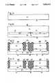
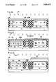
- FIGS. 1a, 1b, 1c, 1d, 1e, 1f, 1g, 1h, 1i, 1j, 1k, 1l, 1m, and 1nare cross-sectional side structural views representing steps in a process for manufacturing a bipolar transistor and an insulated-gate FET according to the invention.
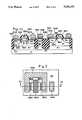
- FIG. 2is a top view of part of the structure in FIG. 1n. For convenience, the areas representing electrically conductive material in FIG. 2 are shaded the same as in FIG. 1n even though FIG. 2 is not a cross-sectional view.
- FIG. 1nis taken through plane 1n--1n in FIG. 2.
- FIGS. 1a-1nillustrate how a vertical NPN transistor and a P-channel insulated-gate FET of the LDD type are fabricated according to the teachings of the invention.
- Phosphorus, arsenic, and antimonyare used selectively as the N-type semiconductor impurities for creating the various regions of N-type conductivity.
- Boronis the complementary P-type dopant.
- each of these elementsis preferably implanted in its singly ionized form.
- the various anneals described beloware used to repair implant lattice damage, activate the implanted species, and drive the species outward (by amounts depending on the species type and the anneal conditions). Certain of the implantations may be replaced by diffusions.
- N-channel insulated-gate FETis typically fabricated with the P-channel FET and the NPN transistor in the overall device structure to achieve a bipolar/complementary-FET arrangement.
- the additional steps needed for manufacturing the N-channel deviceare not given below since they are not material to the invention.
- Substrate 10is converted into the monocrystalline silicon body shown in FIG. 1b by selectively implanting antimony into the upper substrate material at the general locations for heavily doped N-type buried regions 12 and 14, thermally driving the antimony, selectively implanting boron into the upper substrate material at the general location for a heavily doped P-type buried web 16, removing about 1,400 angstroms of silicon along the upper substrate surface, and then growing an arsenic-doped (100) epitaxial layer 18 to a thickness of 12,000 angstroms. These operations are accomplished with the assistance of various thermal oxidation, masking, and etching steps of a conventional nature.
- the antimony implant doseis 2.4 ⁇ 10 15 ions/cm 2 .
- the boron implant doseis 3 ⁇ 10 13 ions/cm 2 .
- P+ buried web 16laterally surrounds each of N+ buried regions 12 and 14.
- N- epitaxial layer 18has a resistivity of about 0.4 ohm-cm.
- a recessed web-like isolation region 20 of silicon dioxideis formed along the upper silicon surface as depicted in FIG. 1c.
- Oxide-isolation region 20penetrates all the way through epitaxial layer 18 and slightly into substrate 16.
- Region 20is formed according to the well-known "LOCOS" technique.
- N+ buried regions 12 and 14expand somewhat during the formation of oxide 20.
- P+ buried web 16grows considerably.
- expitaxial layer 18The remaining portions of expitaxial layer 18 are represented as items 18A, 18B, and 18C. Portions 12, 18A, and 18B form a major N-type region R1 for the NPN transistor. Portions 14 and 18C form a major N-type region R2 for the P-channel FET. Oxide region 20 in combination with web 16 laterally separates regions R1 and R2.
- a planarization operationis performed to reduce the amount of upper surface roughness present at the end of the LOCOS operation.
- the preferred way for doing thisentails thermally growing about 750 angstroms of silicon dioxide along the upper silicon surfaces and then depositing 3,000-5,000 angstroms of boro-phosphosilicate glass (BPSG) on the top of the resultant structure.
- BPSGboro-phosphosilicate glass
- the BPSGis provided with a largely planar upper surface by heating the structure at 1,000° C. for 30 minutes in dry oxygen.
- a combination of dry (plasma) and wet (chemical) etchingis employed to remove a largely uniform thickness of the BPSG and silicon dioxide down to the upper silicon surface.
- FIG. 1dshows the result.
- Layers 22A, 22B, and 22C of silicon dioxideare thermally grown along the upper surfaces of epitaxial portions 18A-18C to a thickness of 300 angstroms. See FIG. 1e.
- a photoresist mask 24 having an opening above portion 18Bis then formed on the top of the structure.
- Phosphorusis implanted through oxide layer 22B into portion 18B of region R1 to form a heavily doped N-type collector contact zone 26.
- the implantationis performed at an energy of 80 kiloelectron volts (KEV) and a dosage of 2 ⁇ 10 15 ions/cm 2 .
- arsenicmay be implanted through oxide 22B into portion 18B at 120 KEV and 3 ⁇ 10 15 ions/cm 2 .
- the arsenicremains near the upper monosilicon surface during subsequent processing steps to prevent blanket P-type implants from counterdoping N+ zone 26.
- the structureis annealed at 1,000° C. for 90 minutes in nitrogen. N+ contact zone 26 moves downward during the anneal. An etch is then performed to remove oxide layers 22A-22C.
- Layers 28A, 28B, and 28C of high-quality silicon dioxideare thermally grown to a thickness of 200 angstroms along the upper surfaces of N- portions 18A-18C. See FIG. 1f.
- Oxide layers 28A -28Care preferably created by subjecting the structure to dry oxygen and tri-chloroethane for 20 minutes at 950° C. and then annealing at the same temperature for 10 minutes in nitrogen to relieve oxide stress. Part of layer 28C later serves as the gate dielectric for the FET. By this time, N+ collector contact 26 has expanded substantially down to buried region 12.
- a blanket layer 30 of amorphous silicon having a thickness of 250 angstromsis deposited on oxide region 20 and on oxide layers 28A-28C. Layer 30 protects oxide 28C from being damaged during subsequent photoresist mask fabrication.
- arsenicis implanted at a low dosage into region 18C to adjust the FET threshold voltage.
- the doseis typically 1 ⁇ 10 12 ions/cm 2 .
- a photoresist mask 32 having an opening above epitaxial portion 18Ais formed on amorphous silicon layer 30 as indicated in FIG. 1f.
- An initial boron implantationis performed through layers 30 and 28A into portion 18A of region R1 to form a primary P-type zone 34 along the upper surface of portion 18A.
- the implant conditionsare 20 KEV and 3-4 ⁇ 10 13 ions/cm 2 .
- the boronreaches a peak concentration about 300 angstroms below the upper silicon surface of region R1.
- N-type region 36generally indicates the location of the phosphorus implanted into portion 18A. The order in which P zone 34 and N region 36 are formed is not material.
- amorphous siliconis deposited on the upper surface of the structure to create a blanket amorphous silicon layer 38.
- the remainder of layer 30forms part of layer 38.
- a photoresist mask 40having an opening above N+ portion 18A and usually above N+ zone 26 is preferably formed on layer 38.
- Arsenicis implanted into the exposed portion of layer 38 at 1 ⁇ 10 16 ions/cm 2 and 80 KEV.
- the dashed line in FIG. 1gindicates the separation between the heavily doped N-type amorphous silicon and the undoped amorphous silicon.
- a photoresist mask 42is formed on amorphous silicon layer 38 as shown in FIG. 1h.
- Mask 42has blocking areas generally above the intended locations for the emitter of the NPN transistor and the gate electrode of the FET.
- a dry etchis performed to remove the entire thickness of the exposed portions of layer 38. The remaining portions consist of patterned amorphous silicon layers 38A and 38C. The dry etch is continued into P zone 34 to remove 500-1,500 angstroms of monosilicon generally situated to the sides of the intended emitter location.
- Mask 42is subsequently removed.
- a thermal oxidationis performed to create layers 44A, 44B, and 44C of silicon dioxide from the exposed silicon along the upper surface of the structure, including the monosilicon below the exposed portions of oxide layers 28B and 28C. See FIG. 1i.
- the thermal oxidationis accomplished by subjecting the structure to dry oxygen for 10 minutes at 920° C. and then annealing at the same temperature for 20 minutes in nitrogen.
- the change in oxide thickness along the monosilicon at the top of the structureis about 125 angstroms.
- the oxide thickness along the amorphous siliconvaries from 250 angstroms to 400 angstroms.
- An intermediate boron implantationis performed into the material along the upper surface of the structure as shown in FIG. 1j in a direction substantially perpendicular to the lower surface of substrate 10.
- the implant conditionsare 2.5 ⁇ 10 13 ions/cm 2 and 20 KEV.
- the boronpasses through the horizontal portions of oxide layers 44A and 44C into the underlying silicon to form (1) a pair of laterally separated intermediate P-type zones 48A along the upper surface of P zone 34 in region R1 and (2) a pair of laterally separated auxiliary P-type S/D zones 48C along the upper surface of portion 18C in region R2. See FIG. 1j.
- Patterned layers 38A and 38C and the vertical portions of oxide layers 44A and 44Cact as an implantation shield to prevent the boron from entering the portions of regions R1 and R2 that they cover.
- the intermediate boron implantdoes not have any significant effect on the doping of patterned layer 38A.
- patterned layer 38Cbecomes P doped.
- N+ contact zone 26may be protected by a photoresist mask 50 which is removed after the implantation. If mask 50 is not used, the implant does not significantly affect the doping of zone 26.
- Electrically insulating spacers 52A and 52Care provided along the sides of patterned layers 38A and 38C as shown in FIG. 1k.
- 3,000-5,000 angstroms of silicon dioxideis deposited on the top of the structure after which a highly anisotropic dry etch is performed to remove all of the deposited and thermally grown oxide except for sidewall spacers 52A and 52C. Oxide layers 44A-44C are thereby substantially removed except for the portions incorporated into spacers 52A and 52C.
- a thermal oxidationis performed to densify spacers 52A and 52C and to create silicon dioxide layers 54A, 54B, and 54C from the exposed silicon along the upper structural surface. See FIG. 1l.
- the oxidationis done in nitrogen with 10% oxygen for 30 minutes at 875° C.
- the resulting oxide thickness along the monosiliconis about 100 angstroms.
- the oxide thickness along the non-monocrystalline siliconis about 200 angstroms.
- a layer 56 of silicon dioxideis then deposited on the top of the structure to a thickness of 300-500 angstroms. Spacers 52A and 52C include the adjoining portions of oxide layer 56.
- a further boron implantationis performed into the material along the upper surface of the structure in a direction substantially perpendicular to the lower substrate surface.
- the implant conditionsare 5-10 ⁇ 10 14 ions/cm 2 and 25 KEV.
- the boronpasses through oxide layers 56, 54A, and 54C into the underlying silicon to form (1) a pair of laterally separated heavily doped P-type base contact zones 58A along the upper surfaces of P zones 48A in region R1 and (2) a pair of laterally separated heavily doped main P-type S/D zones 58C along the upper surfaces of P zones 48C in region R2.
- Patterned layers 38A and 38C and spacers 52A and 52Cact as an implantation shield to protect the silicon that lies below them.
- the further boron implantationdoes not significantly affect the doping of layer 38A.
- Layer 38Cbecomes heavily P doped.
- Contact zone 26may be protected by a photoresist mask 60 which is removed after the implantation. If mask 60 is not present, the doping of zone 26 is still not significantly affected provided that the above-mentioned arsenic implant into region 18B was performed.
- a rapid thermal annealis performed on the structure for 1-20 seconds at 1,000° C. or more in an inert environment.
- the RTAis preferably done for 10 seconds at 1,050° C. in nitrogen.
- the RTAbreaks up any thin native silicon dioxide layer (typically no more than 20 angstroms thick) present along the interface between emitter 46 and overlying patterned layer 38A.
- the structuremay also be annealed at 800°-900° C. for 30 minutes in nitrogen. During the anneal(s), P zones 48A and 48C and P+ zones 58A and 58C expand to the positions generally shown in FIG. 1m.
- a wet etchis performed to remove oxide layers 56 and 54A-54C. Spacers 52A and 52C are otherwise left substantially intact. Due to the various high-temperature operations that the structure has undergone, the silicon in layers 38A and 38C is now substantially polycrystalline.
- Patterned layer 38is the emitter contact for the NPN transistor.
- the intrinsic base portionwhich substantially consists of that part of P zone 34 directly under emitter 46, has a width (in the vertical direction) of approximately 1,500 angstroms.
- each P zone 48Ais 500-1,500 angstroms greater than that of P zone 34 because of the etching into the monosilicon during the patterning of layer 38.
- each base connection zoneis deeper than the intrinsic base.
- each base connection zonehas a greater dopant concentration than the intrinsic base.
- the resistance per unit length (in the direction perpendicular to the plane of FIG. 1m) of the composite extrinsic base formed by the two connection zones in combination with contact zones 58Afalls into a range of 30-100 ohms/micron from run to run.
- the peripheral emitter-base capacitance per unit lengthis 0.25 femtofarad/micron or less.
- the emitter-base breakdown voltagetypically equals 6 volts and, in any case, does not fall below 5 volts.
- the collector for the NPN deviceconsists of N+ regions 12 and 26 and the remaining N-type portions of regions 18A and 36. Buried region 12 serves both as the main (or active) part of the collector and as a connection zone to collector contact zone 26.
- Layer 38Cis the gate electrode for the P-channel FET.
- the remainder of oxide layer 28Cis the gate dielectric.
- Each pair of continuous S/D portions 48C and 58Cforms a composite source/drain zone in an LDD configuration.
- Gate electrode 38Coverlaps the LDD portion of each of the composite S/D zones by an amount that falls into a run-to-run range of 500-1,000 angstroms. This is adequate to achieve very good FET operation.
- the structureis subsequently provided with a first metallization layer for an electrical interconnection system.
- Platinumis blanket deposited on the upper surface of the structure to the thickness of 250-350 angstroms.
- the platinum on the silicon areasis reacted with the underlying silicon according to the conventional "salicide" technique to form PtSi layers 62A, 62B, and 62C as indicated in FIG. 1n.
- the unreacted platinumlocated on the oxide areas) is removed.
- Titanium-tungstenis deposited on the upper surface to a thickness of 1,000 angstroms. This is followed by 3,000 angstroms of aluminum with 1% copper and then another 1,000 angstroms of titanium-tungsten. Using a photoresist mask (not shown), the exposed portions of the upper Ti-W layer are removed. After removing the photoresist, the exposed portions of the aluminum are etched away using the remainder of the upper Ti-W layer as a shield. The remaining portions of the aluminum are denoted as items 64A, 64B, and 64C in FIG. 1n.
- FIG. 2it shows a top view of the first-level metallization pattern for the NPN transistor.
- Al layer 64A for base contact zones 58Ais shaped like an upside down "U” to contact both of zones 58A.
- the dashed line in FIG. 2represents the inside walls of oxide-isolation region 20.
- oxide layers 44A-44Ccould be eliminated.
- only patterned layers 38A and 38Cwould act as an implantation shield over epitaxial portions 18A and 18C during the implantation of P zones 48A and 48C.
- the major part of the width of sidewall spacers 52A and 52Ccould be created by thermal oxidation rather than oxide deposition.
- Polysiliconmay be used to create non-monocrystalline layers 30 and 38. By eliminating mask 40, patterned layer 38C for the gate electrode could be doped N-type. The FET threshold voltage would then be adjusted by implanting a P-type impurity into N- layer 18C. Semiconductor materials of opposite conductivity to those described above may be employed to achieve the same results. Various modifications and applications may thus be made by those skilled in the art without departing from the true scope and spirit of the invention as defined in the appended claims.
Landscapes
- Engineering & Computer Science (AREA)
- Physics & Mathematics (AREA)
- Condensed Matter Physics & Semiconductors (AREA)
- General Physics & Mathematics (AREA)
- Manufacturing & Machinery (AREA)
- Computer Hardware Design (AREA)
- Microelectronics & Electronic Packaging (AREA)
- Power Engineering (AREA)
- Bipolar Transistors (AREA)
Abstract
Description
Claims (20)
Priority Applications (1)
| Application Number | Priority Date | Filing Date | Title |
|---|---|---|---|
| US07/440,456US5006476A (en) | 1988-09-07 | 1989-11-20 | Transistor manufacturing process using three-step base doping |
Applications Claiming Priority (2)
| Application Number | Priority Date | Filing Date | Title |
|---|---|---|---|
| US24152688A | 1988-09-07 | 1988-09-07 | |
| US07/440,456US5006476A (en) | 1988-09-07 | 1989-11-20 | Transistor manufacturing process using three-step base doping |
Related Parent Applications (1)
| Application Number | Title | Priority Date | Filing Date |
|---|---|---|---|
| US24152688AContinuation | 1988-09-07 | 1988-09-07 |
Publications (1)
| Publication Number | Publication Date |
|---|---|
| US5006476Atrue US5006476A (en) | 1991-04-09 |
Family
ID=26934362
Family Applications (1)
| Application Number | Title | Priority Date | Filing Date |
|---|---|---|---|
| US07/440,456Expired - LifetimeUS5006476A (en) | 1988-09-07 | 1989-11-20 | Transistor manufacturing process using three-step base doping |
Country Status (1)
| Country | Link |
|---|---|
| US (1) | US5006476A (en) |
Cited By (42)
| Publication number | Priority date | Publication date | Assignee | Title |
|---|---|---|---|---|
| US5124271A (en)* | 1990-06-20 | 1992-06-23 | Texas Instruments Incorporated | Process for fabricating a BiCMOS integrated circuit |
| US5225377A (en)* | 1991-05-03 | 1993-07-06 | Honeywell Inc. | Method for micromachining semiconductor material |
| US5250448A (en)* | 1990-01-31 | 1993-10-05 | Kabushiki Kaisha Toshiba | Method of fabricating a miniaturized heterojunction bipolar transistor |
| US5268312A (en)* | 1992-10-22 | 1993-12-07 | Motorola, Inc. | Method of forming isolated wells in the fabrication of BiCMOS devices |
| FR2700418A1 (en)* | 1993-01-12 | 1994-07-13 | France Telecom | Electronic component capable of negative dynamic resistance and corresponding manufacturing process. |
| US5371023A (en)* | 1991-06-11 | 1994-12-06 | Hitachi, Ltd. | Gate circuit, semiconductor integrated circuit device and method of fabrication thereof, semiconductor memory and microprocessor |
| US5405789A (en)* | 1992-10-23 | 1995-04-11 | U.S. Philips Corporation | Method of manufacturing a semiconductor device whereby a laterally bounded semiconductor zone is formed in a semiconductor body in a self-aligning manner |
| US5444004A (en)* | 1994-04-13 | 1995-08-22 | Winbond Electronics Corporation | CMOS process compatible self-alignment lateral bipolar junction transistor |
| US5443994A (en)* | 1990-04-02 | 1995-08-22 | National Semiconductor Corporation | Method of fabricating a semiconductor device having a borosilicate glass spacer |
| US5449627A (en)* | 1994-12-14 | 1995-09-12 | United Microelectronics Corporation | Lateral bipolar transistor and FET compatible process for making it |
| WO1996008039A1 (en)* | 1994-09-02 | 1996-03-14 | National Semiconductor Corporation | Structure and fabrication of bipolar transistors with improved output current-voltage characteristics |
| US5500378A (en)* | 1992-12-14 | 1996-03-19 | Sony Corporation | Process for forming a bipolar type semiconductor device |
| US5501991A (en)* | 1994-07-13 | 1996-03-26 | Winbond Electronics Corporation | Process for making a bipolar junction transistor with a self-aligned base contact |
| EP0709894A1 (en)* | 1994-10-28 | 1996-05-01 | Consorzio per la Ricerca sulla Microelettronica nel Mezzogiorno - CoRiMMe | High-frequency bipolar transistor structure, and related manufacturing process |
| US5516718A (en)* | 1992-12-07 | 1996-05-14 | At&T Global Information Solutions Company | Method of making BI-CMOS integrated circuit having a polysilicon emitter |
| US5525532A (en)* | 1994-06-08 | 1996-06-11 | Hyundai Electronics Industries Co., Ltd. | Method for fabricating a semiconductor device |
| US5541134A (en)* | 1993-08-13 | 1996-07-30 | Texas Instruments Incorporated | Bicmos process that supports merged devices |
| US5557131A (en)* | 1992-10-19 | 1996-09-17 | At&T Global Information Solutions Company | Elevated emitter for double poly BICMOS devices |
| US5581115A (en)* | 1994-10-07 | 1996-12-03 | National Semiconductor Corporation | Bipolar transistors using isolated selective doping to improve performance characteristics |
| US5629547A (en)* | 1991-04-23 | 1997-05-13 | Intel Corporation | BICMOS process for counter doped collector |
| US5643809A (en)* | 1995-03-08 | 1997-07-01 | Integrated Device Technology, Inc. | Method for making high speed poly-emitter bipolar transistor |
| US5643810A (en)* | 1995-10-06 | 1997-07-01 | Samsung Electronics Co., Ltd. | Methods of forming BiCMOS semiconductor devices |
| US5654213A (en)* | 1995-10-03 | 1997-08-05 | Integrated Device Technology, Inc. | Method for fabricating a CMOS device |
| US5804476A (en)* | 1995-11-30 | 1998-09-08 | Samsung Electronics Co., Ltd. | Method of forming BiCMOS devices having mosfet and bipolar sections therein |
| US5869380A (en)* | 1998-07-06 | 1999-02-09 | Industrial Technology Research Institute | Method for forming a bipolar junction transistor |
| US6011283A (en)* | 1992-10-19 | 2000-01-04 | Hyundai Electronics America | Pillar emitter for BiCMOS devices |
| US6043130A (en)* | 1999-05-17 | 2000-03-28 | National Semiconductor Corporation | Process for forming bipolar transistor compatible with CMOS utilizing tilted ion implanted base |
| US6051850A (en)* | 1995-12-30 | 2000-04-18 | Fairchild Korea Semiconductor Ltd. | Insulated gate bipolar junction transistors having built-in freewheeling diodes therein |
| US6124180A (en)* | 1991-04-23 | 2000-09-26 | Intel Corporation | BiCMOS process for counter doped collector |
| US6165826A (en)* | 1994-12-23 | 2000-12-26 | Intel Corporation | Transistor with low resistance tip and method of fabrication in a CMOS process |
| US6249030B1 (en) | 1992-12-07 | 2001-06-19 | Hyundai Electronics Industries Co., Ltd. | BI-CMOS integrated circuit |
| US6262472B1 (en) | 1999-05-17 | 2001-07-17 | National Semiconductor Corporation | Bipolar transistor compatible with CMOS utilizing tilted ion implanted base |
| US6444547B2 (en)* | 1997-12-25 | 2002-09-03 | Rohm Co., Ltd. | Method for manufacturing semiconductor device |
| US20030042574A1 (en)* | 2001-09-06 | 2003-03-06 | Stmicroelectronics S.A. | Contact structure on a deep region formed in a semiconductor substrate |
| US20030092222A1 (en)* | 2001-11-09 | 2003-05-15 | Bartlett Donald M. | Circuit isolation utilizing MeV implantation |
| US6720223B2 (en)* | 2002-04-30 | 2004-04-13 | Hewlett-Packard Development Company, L.P. | Power |
| US6724050B2 (en)* | 2002-01-18 | 2004-04-20 | Texas Instruments Incorporated | ESD improvement by a vertical bipolar transistor with low breakdown voltage and high beta |
| US20050020003A1 (en)* | 2001-05-04 | 2005-01-27 | Ted Johansson | Semiconductor process and integrated circuit |
| US20070069309A1 (en)* | 2005-09-26 | 2007-03-29 | Richard Lindsay | Buried well for semiconductor devices |
| US20070275535A1 (en)* | 2004-11-10 | 2007-11-29 | Khater Marwan H | Bipolar transistor with self-aligned retrograde extrinsic base implant profile and self-aligned silicide |
| US9425115B2 (en)* | 2012-04-30 | 2016-08-23 | Freescale Semiconductor, Inc. | Glass frit wafer bond protective structure |
| US20170221987A1 (en)* | 2016-01-29 | 2017-08-03 | Infineon Technologies Ag | Semiconductor Device and a Method for Forming a Semiconductor Device |
Citations (6)
| Publication number | Priority date | Publication date | Assignee | Title |
|---|---|---|---|---|
| JPS59114861A (en)* | 1982-12-21 | 1984-07-03 | Nec Corp | semiconductor equipment |
| JPS6050920A (en)* | 1983-08-30 | 1985-03-22 | Toshiba Corp | Manufacture of semiconductor device |
| JPS60103669A (en)* | 1983-11-10 | 1985-06-07 | Mitsubishi Electric Corp | Semiconductor device and manufacture thereof |
| US4539744A (en)* | 1984-02-03 | 1985-09-10 | Fairchild Camera & Instrument Corporation | Semiconductor planarization process and structures made thereby |
| US4587718A (en)* | 1984-11-30 | 1986-05-13 | Texas Instruments Incorporated | Process for forming TiSi2 layers of differing thicknesses in a single integrated circuit |
| GB2168845A (en)* | 1984-12-20 | 1986-06-25 | Mitsubishi Electric Corp | Electrode arrangement for semiconductor devices |
- 1989
- 1989-11-20USUS07/440,456patent/US5006476A/ennot_activeExpired - Lifetime
Patent Citations (6)
| Publication number | Priority date | Publication date | Assignee | Title |
|---|---|---|---|---|
| JPS59114861A (en)* | 1982-12-21 | 1984-07-03 | Nec Corp | semiconductor equipment |
| JPS6050920A (en)* | 1983-08-30 | 1985-03-22 | Toshiba Corp | Manufacture of semiconductor device |
| JPS60103669A (en)* | 1983-11-10 | 1985-06-07 | Mitsubishi Electric Corp | Semiconductor device and manufacture thereof |
| US4539744A (en)* | 1984-02-03 | 1985-09-10 | Fairchild Camera & Instrument Corporation | Semiconductor planarization process and structures made thereby |
| US4587718A (en)* | 1984-11-30 | 1986-05-13 | Texas Instruments Incorporated | Process for forming TiSi2 layers of differing thicknesses in a single integrated circuit |
| GB2168845A (en)* | 1984-12-20 | 1986-06-25 | Mitsubishi Electric Corp | Electrode arrangement for semiconductor devices |
Non-Patent Citations (10)
| Title |
|---|
| Alverez et al., "2 Micron Merged Bipolar-CMOS Technology", IEDM Tech. Dig., Dec. 9-12, 1984, pp. 761-764. |
| Alverez et al., 2 Micron Merged Bipolar CMOS Technology , IEDM Tech. Dig., Dec. 9 12, 1984, pp. 761 764.* |
| Chen et al., "An Advanced Bipolar Transistor with Self-Aligned Ion-Implanted Base and W/Poly Emitter", IEEE Trans. Elec. Devs., vol. 35, No. 8, 8/88, pp. 1322-1327. |
| Chen et al., An Advanced Bipolar Transistor with Self Aligned Ion Implanted Base and W/Poly Emitter , IEEE Trans. Elec. Devs., vol. 35, No. 8, 8/88, pp. 1322 1327.* |
| Cole, "Is BiCMOS The Next Technology Driver?", Electronics, Feb. 4, 1988, pp. 55-57. |
| Cole, Is BiCMOS The Next Technology Driver , Electronics, Feb. 4, 1988, pp. 55 57.* |
| Cuthbertson et al., "Self-Aligned Transistor with Polysilicon Emitters for Bipolar VLSI", IEEE Trans. Elec. Devs., Feb. 1985, pp. 242-247. |
| Cuthbertson et al., Self Aligned Transistor with Polysilicon Emitters for Bipolar VLSI , IEEE Trans. Elec. Devs., Feb. 1985, pp. 242 247.* |
| Konaka et al., "A 20 ps/G. Si Bipolar IC Using Advanced SST with Collector Ion Implantation," Extended Abs., 19th Conf. Solid State Devs. & Mats., 1987, pp. 331-334. |
| Konaka et al., A 20 ps/G. Si Bipolar IC Using Advanced SST with Collector Ion Implantation, Extended Abs., 19th Conf. Solid State Devs. & Mats., 1987, pp. 331 334.* |
Cited By (61)
| Publication number | Priority date | Publication date | Assignee | Title |
|---|---|---|---|---|
| US5250448A (en)* | 1990-01-31 | 1993-10-05 | Kabushiki Kaisha Toshiba | Method of fabricating a miniaturized heterojunction bipolar transistor |
| US5443994A (en)* | 1990-04-02 | 1995-08-22 | National Semiconductor Corporation | Method of fabricating a semiconductor device having a borosilicate glass spacer |
| US5124271A (en)* | 1990-06-20 | 1992-06-23 | Texas Instruments Incorporated | Process for fabricating a BiCMOS integrated circuit |
| US5374845A (en)* | 1990-06-20 | 1994-12-20 | Texas Instruments Incorporated | Process for reduced emitter-base capacitance in bipolar transistor |
| US6124180A (en)* | 1991-04-23 | 2000-09-26 | Intel Corporation | BiCMOS process for counter doped collector |
| US5629547A (en)* | 1991-04-23 | 1997-05-13 | Intel Corporation | BICMOS process for counter doped collector |
| US5225377A (en)* | 1991-05-03 | 1993-07-06 | Honeywell Inc. | Method for micromachining semiconductor material |
| US5371023A (en)* | 1991-06-11 | 1994-12-06 | Hitachi, Ltd. | Gate circuit, semiconductor integrated circuit device and method of fabrication thereof, semiconductor memory and microprocessor |
| US6011283A (en)* | 1992-10-19 | 2000-01-04 | Hyundai Electronics America | Pillar emitter for BiCMOS devices |
| US5557131A (en)* | 1992-10-19 | 1996-09-17 | At&T Global Information Solutions Company | Elevated emitter for double poly BICMOS devices |
| US5268312A (en)* | 1992-10-22 | 1993-12-07 | Motorola, Inc. | Method of forming isolated wells in the fabrication of BiCMOS devices |
| US5405789A (en)* | 1992-10-23 | 1995-04-11 | U.S. Philips Corporation | Method of manufacturing a semiconductor device whereby a laterally bounded semiconductor zone is formed in a semiconductor body in a self-aligning manner |
| US6249030B1 (en) | 1992-12-07 | 2001-06-19 | Hyundai Electronics Industries Co., Ltd. | BI-CMOS integrated circuit |
| US20030203559A1 (en)* | 1992-12-07 | 2003-10-30 | Lee Steven S. | BI-CMOS integrated circuit |
| US6593178B1 (en) | 1992-12-07 | 2003-07-15 | Hyundai Electronics America | BI-CMOS integrated circuit |
| US5516718A (en)* | 1992-12-07 | 1996-05-14 | At&T Global Information Solutions Company | Method of making BI-CMOS integrated circuit having a polysilicon emitter |
| US6943413B2 (en) | 1992-12-07 | 2005-09-13 | Hynix Semiconductor Inc. | BI-CMOS integrated circuit |
| US5500378A (en)* | 1992-12-14 | 1996-03-19 | Sony Corporation | Process for forming a bipolar type semiconductor device |
| US5465001A (en)* | 1993-01-12 | 1995-11-07 | France Telecom | Electronic component capable of negative dynamic resistance |
| EP0607075A1 (en)* | 1993-01-12 | 1994-07-20 | France Telecom | Electronic component which can have a negative dynamic resistance and process for making the same |
| FR2700418A1 (en)* | 1993-01-12 | 1994-07-13 | France Telecom | Electronic component capable of negative dynamic resistance and corresponding manufacturing process. |
| US5541134A (en)* | 1993-08-13 | 1996-07-30 | Texas Instruments Incorporated | Bicmos process that supports merged devices |
| US5444004A (en)* | 1994-04-13 | 1995-08-22 | Winbond Electronics Corporation | CMOS process compatible self-alignment lateral bipolar junction transistor |
| US5525532A (en)* | 1994-06-08 | 1996-06-11 | Hyundai Electronics Industries Co., Ltd. | Method for fabricating a semiconductor device |
| US5726476A (en)* | 1994-06-08 | 1998-03-10 | Hyundai Electronics Industries Co., Ltd. | Semiconductor device having a particular CMOS structure |
| US5501991A (en)* | 1994-07-13 | 1996-03-26 | Winbond Electronics Corporation | Process for making a bipolar junction transistor with a self-aligned base contact |
| US5525833A (en)* | 1994-07-13 | 1996-06-11 | Winbond Electronics Corporation | Process for making a bipolar junction transistor with a self-aligned base contact |
| US5589409A (en)* | 1994-09-02 | 1996-12-31 | National Semiconductor Corporation | Fabrication of bipolar transistors with improved output current-voltage characteristics |
| WO1996008039A1 (en)* | 1994-09-02 | 1996-03-14 | National Semiconductor Corporation | Structure and fabrication of bipolar transistors with improved output current-voltage characteristics |
| US5548158A (en)* | 1994-09-02 | 1996-08-20 | National Semiconductor Corporation | Structure of bipolar transistors with improved output current-voltage characteristics |
| US5581115A (en)* | 1994-10-07 | 1996-12-03 | National Semiconductor Corporation | Bipolar transistors using isolated selective doping to improve performance characteristics |
| US5698459A (en)* | 1994-10-07 | 1997-12-16 | National Semiconductor Corporation | Fabrication of bipolar transistors using selective doping to improve performance characteristics |
| US5804486A (en)* | 1994-10-28 | 1998-09-08 | Consorzio Per La Ricerca Sulla Microelectronica Nel Mezzogiorno | Process for manufacturing a high-frequency bipolar transistor structure |
| EP0709894A1 (en)* | 1994-10-28 | 1996-05-01 | Consorzio per la Ricerca sulla Microelettronica nel Mezzogiorno - CoRiMMe | High-frequency bipolar transistor structure, and related manufacturing process |
| US5449627A (en)* | 1994-12-14 | 1995-09-12 | United Microelectronics Corporation | Lateral bipolar transistor and FET compatible process for making it |
| US6165826A (en)* | 1994-12-23 | 2000-12-26 | Intel Corporation | Transistor with low resistance tip and method of fabrication in a CMOS process |
| US5643809A (en)* | 1995-03-08 | 1997-07-01 | Integrated Device Technology, Inc. | Method for making high speed poly-emitter bipolar transistor |
| US5654213A (en)* | 1995-10-03 | 1997-08-05 | Integrated Device Technology, Inc. | Method for fabricating a CMOS device |
| US5643810A (en)* | 1995-10-06 | 1997-07-01 | Samsung Electronics Co., Ltd. | Methods of forming BiCMOS semiconductor devices |
| US5804476A (en)* | 1995-11-30 | 1998-09-08 | Samsung Electronics Co., Ltd. | Method of forming BiCMOS devices having mosfet and bipolar sections therein |
| US6051850A (en)* | 1995-12-30 | 2000-04-18 | Fairchild Korea Semiconductor Ltd. | Insulated gate bipolar junction transistors having built-in freewheeling diodes therein |
| US6444547B2 (en)* | 1997-12-25 | 2002-09-03 | Rohm Co., Ltd. | Method for manufacturing semiconductor device |
| US5869380A (en)* | 1998-07-06 | 1999-02-09 | Industrial Technology Research Institute | Method for forming a bipolar junction transistor |
| US6528375B2 (en) | 1999-05-17 | 2003-03-04 | National Semiconductor Corporation | Bipolar transistor compatible with CMOS utilizing tilted ion implanted base |
| US6262472B1 (en) | 1999-05-17 | 2001-07-17 | National Semiconductor Corporation | Bipolar transistor compatible with CMOS utilizing tilted ion implanted base |
| US6043130A (en)* | 1999-05-17 | 2000-03-28 | National Semiconductor Corporation | Process for forming bipolar transistor compatible with CMOS utilizing tilted ion implanted base |
| US20100055860A1 (en)* | 2001-05-04 | 2010-03-04 | Infineon Technologies Ag | Semiconductor Process and Integrated Circuit |
| US20050020003A1 (en)* | 2001-05-04 | 2005-01-27 | Ted Johansson | Semiconductor process and integrated circuit |
| US20030042574A1 (en)* | 2001-09-06 | 2003-03-06 | Stmicroelectronics S.A. | Contact structure on a deep region formed in a semiconductor substrate |
| US6847094B2 (en)* | 2001-09-06 | 2005-01-25 | Stmicroelectronics S.A. | Contact structure on a deep region formed in a semiconductor substrate |
| US20030092222A1 (en)* | 2001-11-09 | 2003-05-15 | Bartlett Donald M. | Circuit isolation utilizing MeV implantation |
| US6885078B2 (en)* | 2001-11-09 | 2005-04-26 | Lsi Logic Corporation | Circuit isolation utilizing MeV implantation |
| US6724050B2 (en)* | 2002-01-18 | 2004-04-20 | Texas Instruments Incorporated | ESD improvement by a vertical bipolar transistor with low breakdown voltage and high beta |
| US6720223B2 (en)* | 2002-04-30 | 2004-04-13 | Hewlett-Packard Development Company, L.P. | Power |
| US20070275535A1 (en)* | 2004-11-10 | 2007-11-29 | Khater Marwan H | Bipolar transistor with self-aligned retrograde extrinsic base implant profile and self-aligned silicide |
| EP1815517A4 (en)* | 2004-11-10 | 2009-08-05 | Ibm | BIPOLAR TRANSISTOR WITH SELF ALIGNMENT SILICURE AND EXTRINSIC BASE |
| US7732292B2 (en) | 2004-11-10 | 2010-06-08 | International Business Machines Corporation | Bipolar transistor with self-aligned retrograde extrinsic base implant profile and self-aligned silicide |
| US20070069309A1 (en)* | 2005-09-26 | 2007-03-29 | Richard Lindsay | Buried well for semiconductor devices |
| US9425115B2 (en)* | 2012-04-30 | 2016-08-23 | Freescale Semiconductor, Inc. | Glass frit wafer bond protective structure |
| US20170221987A1 (en)* | 2016-01-29 | 2017-08-03 | Infineon Technologies Ag | Semiconductor Device and a Method for Forming a Semiconductor Device |
| US10043866B2 (en)* | 2016-01-29 | 2018-08-07 | Infineon Technologies Ag | Semiconductor device and a method for forming a semiconductor device |
Similar Documents
| Publication | Publication Date | Title |
|---|---|---|
| US5006476A (en) | Transistor manufacturing process using three-step base doping | |
| US5424572A (en) | Spacer formation in a semiconductor structure | |
| EP0088922B1 (en) | A method of forming electrodes and wiring strips on a semiconductor device | |
| US5171702A (en) | Method for forming a thick base oxide in a BiCMOS process | |
| US4734382A (en) | BiCMOS process having narrow bipolar emitter and implanted aluminum isolation | |
| US4693782A (en) | Fabrication method of semiconductor device | |
| US4066473A (en) | Method of fabricating high-gain transistors | |
| US4816423A (en) | Bicmos process for forming shallow npn emitters and mosfet source/drains | |
| JPH04226066A (en) | BICMOS device and its manufacturing method | |
| US5554554A (en) | Process for fabricating two loads having different resistance levels in a common layer of polysilicon | |
| US6215160B1 (en) | Semiconductor device having bipolar transistor and field effect transistor and method of manufacturing the same | |
| US4929570A (en) | Selective epitaxy BiCMOS process | |
| KR950006478B1 (en) | Manufacturing method of self-aligned bipolar transistor | |
| US5194926A (en) | Semiconductor device having an inverse-T bipolar transistor | |
| US4871684A (en) | Self-aligned polysilicon emitter and contact structure for high performance bipolar transistors | |
| US20030080394A1 (en) | Control of dopant diffusion from polysilicon emitters in bipolar integrated circuits | |
| JPH04226064A (en) | Interconnect for semiconductor device and method for manufacturing same | |
| US5079177A (en) | Process for fabricating high performance bicmos circuits | |
| EP0233202B1 (en) | Fabricating a semiconductor device with buried oxide | |
| KR970011641B1 (en) | Semiconductor device and manufacturing method | |
| US5443994A (en) | Method of fabricating a semiconductor device having a borosilicate glass spacer | |
| KR0128339B1 (en) | Bipolar Transistor Manufacturing Method Using CMOS Technology | |
| US5348896A (en) | Method for fabricating a BiCMOS device | |
| US6043544A (en) | Semiconductor gate conductor with a substantially uniform doping profile having minimal susceptibility to dopant penetration into the underlying gate dielectric | |
| US5643810A (en) | Methods of forming BiCMOS semiconductor devices |
Legal Events
| Date | Code | Title | Description |
|---|---|---|---|
| STCF | Information on status: patent grant | Free format text:PATENTED CASE | |
| FEPP | Fee payment procedure | Free format text:PAYOR NUMBER ASSIGNED (ORIGINAL EVENT CODE: ASPN); ENTITY STATUS OF PATENT OWNER: LARGE ENTITY | |
| FPAY | Fee payment | Year of fee payment:4 | |
| FPAY | Fee payment | Year of fee payment:8 | |
| FPAY | Fee payment | Year of fee payment:12 | |
| AS | Assignment | Owner name:NXP B.V., NETHERLANDS Free format text:ASSIGNMENT OF ASSIGNORS INTEREST;ASSIGNOR:PHILIPS ELECTRONICS NORTH AMERICA CORP.;REEL/FRAME:018654/0514 Effective date:20061206 Owner name:PHILIPS ELECTRONICS NORTH AMERICAN CORPORATION, NE Free format text:CHANGE OF NAME;ASSIGNOR:NORTH AMERICAN PHILIPS CORPORATION;REEL/FRAME:018654/0565 Effective date:19930524 | |
| AS | Assignment | Owner name:MORGAN STANLEY SENIOR FUNDING, INC., ENGLAND Free format text:SECURITY AGREEMENT;ASSIGNOR:NXP B.V.;REEL/FRAME:018806/0201 Effective date:20061201 | |
| AS | Assignment | Owner name:NXP B.V., NETHERLANDS Free format text:RELEASE BY SECURED PARTY;ASSIGNOR:MORGAN STANLEY SENIOR FUNDING, INC;REEL/FRAME:050315/0443 Effective date:20190903 |