US5001528A - Radiation hardened CMOS on SOI or SOS devices - Google Patents
Radiation hardened CMOS on SOI or SOS devicesDownload PDFInfo
- Publication number
- US5001528A US5001528AUS07/304,759US30475989AUS5001528AUS 5001528 AUS5001528 AUS 5001528AUS 30475989 AUS30475989 AUS 30475989AUS 5001528 AUS5001528 AUS 5001528A
- Authority
- US
- United States
- Prior art keywords
- region
- transistor
- end plugs
- source
- drain
- Prior art date
- Legal status (The legal status is an assumption and is not a legal conclusion. Google has not performed a legal analysis and makes no representation as to the accuracy of the status listed.)
- Expired - Fee Related
Links
- 230000005855radiationEffects0.000titleclaimsabstractdescription13
- 238000002955isolationMethods0.000claimsabstractdescription18
- VYPSYNLAJGMNEJ-UHFFFAOYSA-NSilicium dioxideChemical compoundO=[Si]=OVYPSYNLAJGMNEJ-UHFFFAOYSA-N0.000claimsabstractdescription16
- 235000012239silicon dioxideNutrition0.000claimsabstractdescription8
- 239000000377silicon dioxideSubstances0.000claimsabstractdescription8
- 239000012535impuritySubstances0.000claimsabstractdescription7
- 229910052710siliconInorganic materials0.000claimsdescription10
- 239000010703siliconSubstances0.000claimsdescription10
- 239000012212insulatorSubstances0.000claimsdescription2
- 229910052594sapphireInorganic materials0.000claimsdescription2
- 239000010980sapphireSubstances0.000claimsdescription2
- 230000003071parasitic effectEffects0.000abstractdescription3
- 108091006146ChannelsProteins0.000description21
- 238000013459approachMethods0.000description16
- XUIMIQQOPSSXEZ-UHFFFAOYSA-NSiliconChemical compound[Si]XUIMIQQOPSSXEZ-UHFFFAOYSA-N0.000description9
- 229910052751metalInorganic materials0.000description8
- 239000002184metalSubstances0.000description8
- 230000015556catabolic processEffects0.000description7
- 238000000034methodMethods0.000description7
- 235000012431wafersNutrition0.000description6
- 229910021420polycrystalline siliconInorganic materials0.000description5
- 229920005591polysiliconPolymers0.000description5
- 238000013461designMethods0.000description4
- 238000005516engineering processMethods0.000description4
- XAGFODPZIPBFFR-UHFFFAOYSA-NaluminiumChemical compound[Al]XAGFODPZIPBFFR-UHFFFAOYSA-N0.000description3
- 230000000694effectsEffects0.000description3
- 238000001465metallisationMethods0.000description3
- 238000012986modificationMethods0.000description3
- 230000004048modificationEffects0.000description3
- 239000000758substrateSubstances0.000description3
- 229910052782aluminiumInorganic materials0.000description2
- 230000005540biological transmissionEffects0.000description2
- 238000011161developmentMethods0.000description2
- 238000002513implantationMethods0.000description2
- 238000005510radiation hardeningMethods0.000description2
- 239000004065semiconductorSubstances0.000description2
- 238000012876topographyMethods0.000description2
- ZOXJGFHDIHLPTG-UHFFFAOYSA-NBoronChemical compound[B]ZOXJGFHDIHLPTG-UHFFFAOYSA-N0.000description1
- 108010075750P-Type Calcium ChannelsProteins0.000description1
- 230000002547anomalous effectEffects0.000description1
- QVGXLLKOCUKJST-UHFFFAOYSA-Natomic oxygenChemical compound[O]QVGXLLKOCUKJST-UHFFFAOYSA-N0.000description1
- 230000015572biosynthetic processEffects0.000description1
- 229910052796boronInorganic materials0.000description1
- 230000000295complement effectEffects0.000description1
- 230000001419dependent effectEffects0.000description1
- RGLYKWWBQGJZGM-ISLYRVAYSA-NdiethylstilbestrolChemical compoundC=1C=C(O)C=CC=1C(/CC)=C(\CC)C1=CC=C(O)C=C1RGLYKWWBQGJZGM-ISLYRVAYSA-N0.000description1
- 238000005429filling processMethods0.000description1
- 239000007943implantSubstances0.000description1
- 238000004519manufacturing processMethods0.000description1
- 230000000873masking effectEffects0.000description1
- 229910044991metal oxideInorganic materials0.000description1
- 150000004706metal oxidesChemical class0.000description1
- 150000002739metalsChemical class0.000description1
- 229910052760oxygenInorganic materials0.000description1
- 239000001301oxygenSubstances0.000description1
- 238000012856packingMethods0.000description1
- 238000012545processingMethods0.000description1
- 238000000926separation methodMethods0.000description1
Images
Classifications
- H—ELECTRICITY
- H10—SEMICONDUCTOR DEVICES; ELECTRIC SOLID-STATE DEVICES NOT OTHERWISE PROVIDED FOR
- H10D—INORGANIC ELECTRIC SEMICONDUCTOR DEVICES
- H10D86/00—Integrated devices formed in or on insulating or conducting substrates, e.g. formed in silicon-on-insulator [SOI] substrates or on stainless steel or glass substrates
- H10D86/201—Integrated devices formed in or on insulating or conducting substrates, e.g. formed in silicon-on-insulator [SOI] substrates or on stainless steel or glass substrates the substrates comprising an insulating layer on a semiconductor body, e.g. SOI
- H—ELECTRICITY
- H10—SEMICONDUCTOR DEVICES; ELECTRIC SOLID-STATE DEVICES NOT OTHERWISE PROVIDED FOR
- H10D—INORGANIC ELECTRIC SEMICONDUCTOR DEVICES
- H10D30/00—Field-effect transistors [FET]
- H10D30/60—Insulated-gate field-effect transistors [IGFET]
- H10D30/67—Thin-film transistors [TFT]
- H10D30/6704—Thin-film transistors [TFT] having supplementary regions or layers in the thin films or in the insulated bulk substrates for controlling properties of the device
- H10D30/6708—Thin-film transistors [TFT] having supplementary regions or layers in the thin films or in the insulated bulk substrates for controlling properties of the device for preventing the kink effect or the snapback effect, e.g. discharging the minority carriers of the channel region for preventing bipolar effect
- H—ELECTRICITY
- H10—SEMICONDUCTOR DEVICES; ELECTRIC SOLID-STATE DEVICES NOT OTHERWISE PROVIDED FOR
- H10D—INORGANIC ELECTRIC SEMICONDUCTOR DEVICES
- H10D84/00—Integrated devices formed in or on semiconductor substrates that comprise only semiconducting layers, e.g. on Si wafers or on GaAs-on-Si wafers
- H10D84/80—Integrated devices formed in or on semiconductor substrates that comprise only semiconducting layers, e.g. on Si wafers or on GaAs-on-Si wafers characterised by the integration of at least one component covered by groups H10D12/00 or H10D30/00, e.g. integration of IGFETs
- H10D84/82—Integrated devices formed in or on semiconductor substrates that comprise only semiconducting layers, e.g. on Si wafers or on GaAs-on-Si wafers characterised by the integration of at least one component covered by groups H10D12/00 or H10D30/00, e.g. integration of IGFETs of only field-effect components
- H10D84/83—Integrated devices formed in or on semiconductor substrates that comprise only semiconducting layers, e.g. on Si wafers or on GaAs-on-Si wafers characterised by the integration of at least one component covered by groups H10D12/00 or H10D30/00, e.g. integration of IGFETs of only field-effect components of only insulated-gate FETs [IGFET]
- H10D84/85—Complementary IGFETs, e.g. CMOS
- H10D84/856—Complementary IGFETs, e.g. CMOS the complementary IGFETs having different architectures than each other, e.g. high-voltage and low-voltage CMOS
- Y—GENERAL TAGGING OF NEW TECHNOLOGICAL DEVELOPMENTS; GENERAL TAGGING OF CROSS-SECTIONAL TECHNOLOGIES SPANNING OVER SEVERAL SECTIONS OF THE IPC; TECHNICAL SUBJECTS COVERED BY FORMER USPC CROSS-REFERENCE ART COLLECTIONS [XRACs] AND DIGESTS
- Y10—TECHNICAL SUBJECTS COVERED BY FORMER USPC
- Y10S—TECHNICAL SUBJECTS COVERED BY FORMER USPC CROSS-REFERENCE ART COLLECTIONS [XRACs] AND DIGESTS
- Y10S257/00—Active solid-state devices, e.g. transistors, solid-state diodes
- Y10S257/906—Dram with capacitor electrodes used for accessing, e.g. bit line is capacitor plate
Definitions
- the present inventionis directed to semiconductor devices and particularly to CMOS SOI or SOS devices having radiation hardened characteristics.
- Silicon-on-Insulator (SOI) technologyhas received considerably attention recently for development of high-density, radiation-hardened integrated circuits.
- the technologyoffers good potential for achieving a combination of radiation hardness and circuit density levels not attainable by bulk complementary metal oxide semiconductor (CMOS) or dielectrically isolated bipolar implementations.
- CMOScomplementary metal oxide semiconductor
- Interest in the technologyhas also been amplified by the recent availability of improved-quality oxygen-implanted SOI wafers.
- the SIMOX (Separation by IMplanted OXygen) approachis being considered as a production-capable process for providing high-quality SOI wafers.
- S. S. TsaoD. M. Fleetwood, H. T. Weaver, L.
- CMOS/SOI radiation hardeningIn CMOS/SOI radiation hardening, recent emphasis has mostly been on sidewall isolation, and two isolation approaches have been reported,
- the isolated mesa approach(with sloped sidewall) is an extension of device isolation techniques employed in CMOS/SOS where a MOS device is formed on a silicon layer on top of a sapphire substrate. Hardening of the sidewall in this case is implemented by using an appropriate hardened gate dielectric on the sidewall.
- the sidewall transistorhas different characteristics than the top channel transistor.
- the sidewall channelalso connects the top channel to the back channel, which is not desirable due to potential corner effects: at the corners, the channel sees both the sidewall gate dielectric and the buried oxide.
- Planarized polysilicon-filled trench isolationis another technique that has been applied for sidewall hardening.
- the sidewall hardness problemexists for oxide-isolated NMOS transistors because the channel along the sidewall can invert due to charge buildup in the isolation oxide.
- the charge buildup problemcan be reduced.
- this approachrequires both the growth of a hardened gate oxide on the sidewall and a fairly difficult trench-definition-and-filling process, and these two requirements are not necessarily compatible.
- An important advantage of CMOS/SOI (or SOS)is its relative simplicity in device structure as compared to bulk CMOS. The addition of a difficult trench isolation process would detract from this advantage.
- An object of the present inventionis to provide a radiation hardened N or P type CMOS SOI or SOS transistor in which end plugs are formed at each end of a floating transistor body and are electrically connected through metallized contacts to a source region so that the body no longer floats.
- the bodyis electrically tied to the source region, thus preventing the formation of a bipolar transistor operation at the channel region which could be turned on by a ⁇ radiation pulse.
- the end plugsseparate the MOS sidewall from an isolation oxide, thereby solving a problem of radiation-induced turn-on of the sidewall transistor in a total dose environment.
- a radiation hardened CMOS transistorcomprises a source region, a drain region and a channel region formed on an SOI or SOS wafer.
- the conductivity of the source, drain and channel regionsmay be selected to form either an NMOS or PMOS type transistor.
- End plugs having a conductivity opposite that of the source region and drain regionare connected to the channel region.
- the entire transistoris surrounded with a silicon dioxide isolation region.
- the end plugsextend along opposite ends of the source region but not along the drain region, so as not to create a potential low breakdown voltage and excess leakage current condition between the drain and source.
- the end plugsextend along opposite ends of the source region and the drain region, and the drain region includes portions adjacent the end plugs having an impurity concentration which is significantly lower than the impurity concentration of the remainder of the drain region.
- Contract holes for establishing electrical contact with the transistorare positioned over areas in which the source region interfaces with each of the end plugs, and also over the area of the drain region.
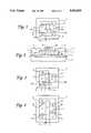
- FIG. 1is a top plan view of an N MOS transistor fabricated to the stage of contact hole placement and before metal deposition.
- FIG. 2is a cross sectional view of FIG. 1 taken along the lines A--A thereof.
- FIG. 3is a top plan view of an NMOS transistor similar to that shown in FIG. 1 further illustrating a second modification of the layout for improving the drain-source breakdown voltage.
- FIG. 4is a top plan view of an N MOS transistor similar to that shown in FIG. 1 further illustrating a second modification of the layout for improving the drain-source breakdown voltage.
- the present inventionis a modification of the oxide-isolated NMOS (or PMOS) transistor formed on an SOI or SOS substrate, often referred to as the floating body transistor.
- the transistor of the present inventioncomprises a silicon island 1 formed on top of a buried oxide 4 on top of a silicon substrate 6.
- Source 2a and drain 2b regions of n+ conductivityare formed in the island, along with a channel region 3 of p conductivity which forms a transistor body.
- a gate oxide 4ais formed on top of the channel region 3, and a polysilicon gate 5 (or metal gate) is formed on top of the gate oxide 4a.
- Silicon end plugs 6 of p+ conductivityare implanted at opposite ends of the silicon island 1, as shown in FIG. 1.
- a silicon dioxide isolation region 7surrounds and covers the end plugs 6 and the silicon island 1.
- Each end plug 6is connected to the channel region 3, and may also be connected to the source region 2a through contact holes 9, as shown in FIG. 1.
- An additional contact hole 9is provided through the silicon dioxide isolation region 7 to drain region 2b.
- the contact holes 9overlap the boundary between the source region 2a and the end plugs 6.
- Metal lines(not shown) may be laid over the contact holes 9 to provide electrical connection to source region 2a and drain region 2b, and to polysilicon gate 5 outside the area of the transistor.
- the metal linesmay be made of aluminum, aluminum/silicon, or other metals.
- the end plugs 6are electrically connected to the source region 2a, since the source region and end plugs have common contact holes 9 and metal lines. Since the end plugs 6 are connected to the channel region 3, the source region 2a is also electrically connected to the
- the SOI wafer structurelends itself very well to a simple oxide isolation process with planar wafer topography for CMOS/SOI.
- the present inventionuses this approach with a modified transistor layout design for solving sidewall and floating body radiation hardening problems.
- the width of the silicon island 1 along the channel region widthis increased beyond the active transistor area in order to incorporate the two end plugs 6 which are doped for p+ for NMOS transistors (and n+ for PMOS transistors).
- the NMOS sidewall channel regionno longer intersects the field oxide (silicon dioxide isolation region 7) and only highly doped p+ silicon regions of the end plugs are adjacent to the field oxide.
- the total dose radiationgenerates positive charge in the silicon dioxide isolation region 7. If the oxide were adjacent to the channel region sidewall, the induced positive charge buildup would invert the sidewall and cause sidewall leakage.
- the structure according to the inventionprevents this problem.
- Floating body MOS transistorsexhibit an anomalous subthreshold slope behavior and the kink effect in the I-V characteristics.
- the kink effectcan be minimized by using very thin, fully-depleted SOI films.
- parasitic bipolar transistorassociated with the drain-body-source junctions of the MOS transistor. In an intense ⁇ environment, photocurrents in the drain-body and source-body biodes could cause the parasitic bipolar transistor to turn on and result in an upset in a memory circuit.
- the end plugs 6are connected to the channel region 3.
- the sourceis electrically connected, i.e., tied to the body, by the source metallization if the source region 2a and the end plugs 6 have common contact holes, such as illustrated by the contact holes 9 in FIG. 1.
- Thiseliminates the problem of a floating body which is inherent in the isolated mesa approach and in trench-isolation designs.
- the sourcecan be tied to the body in every transistor so that the problem of voltage-dependent variation of threshold voltage of a load transistor in analog MOS is greatly reduced, amplified linearity can be significantly improved.
- the bodyIn transmission gates, the body cannot be tied to the source, but is connected to a voltage rail.
- the end plugs 6 and the source region 2acannot share the same contact holes, and a separate contact is required for the end plug to permit tying the body to V SS (or V DD ). This will consume extra area, however, transmission gates do not occur very often in random logic LSI, and the added area penalty should not be appreciable.
- An important advantage of the hardening approach of the present inventionis its simplicity and ease of fabrication. No special or complicated processing is needed.
- the source metallizationautomatically ties the source to the body, and both n+ and p+ processes are available in CMOS. Therefore, the end plugs can be incorporated without any increase in the number of masking steps.
- the end plugscan be incorporated without any increase in the number of masking steps.
- a satisfactory impurity rangeis now 10.sup. ⁇ -10 18 per cc.
- FIG. 3shows a modified structure with shortened p+ end plugs 6 which do not contact with the drain region 2b.
- the end plugs 6terminate inside the channel region 3, less than 1 mm from the edge of the drain region 2b.
- the drain n+-p+ diodeis eliminated and the low breakdown voltage problem is removed.
- This structurewill still be hard to total dose because a p-type channel does not exist next to the silicon dioxide isolation region 7.
- the embodiment of FIG. 3has been implemented and has achieved low leakage currents, greatly improved breakdown voltage, and good radiation tolerance.
- FIG. 4Another approach shown in FIG. 4 is to shorten the drain n+ implant mask by about 1 ⁇ m from the sidewall ends. The resulting transistor will then have an n region 14 between the n+ drain region 2b and the p+ end plugs 6, as illustrated in FIG. 4. This approach replaces the drain n+-p+ diode with a n+-n-p+ diode, having a very narrow n region. As a result, the breakdown voltage problem should be significantly improved.
- the sidewall hardening approach of the present inventionis consistent with achieving a high packing density and is comparable to the isolated mesa approach (with sloped sidewall).
- layout design rulesrequire that the polysilicon gate extend beyond the area of the active transistor island.
- the end plug widthis only slightly larger than the poly gate extension.
- the poly gatemust extend further if aluminum metal is to be tied to the poly gate.
- layout rulesrequire that the contact hole to the poly and the metal line be placed at at safe distance from the edge of the active region.
- the edge of the metal linecan coincide with the edge of the transistor channel, and the contact hole to the poly can be placed right on top of the end plug.
- the present designis better than the isolated mesa approach.
Landscapes
- Thin Film Transistor (AREA)
Abstract
Description
The United States Government has rights in this invention pursuant to Contract No. F19628-86-C-0074 between the U.S. Government and Northrop Corporation.
The present invention is directed to semiconductor devices and particularly to CMOS SOI or SOS devices having radiation hardened characteristics.
Silicon-on-Insulator (SOI) technology has received considerably attention recently for development of high-density, radiation-hardened integrated circuits. The technology offers good potential for achieving a combination of radiation hardness and circuit density levels not attainable by bulk complementary metal oxide semiconductor (CMOS) or dielectrically isolated bipolar implementations. Interest in the technology has also been amplified by the recent availability of improved-quality oxygen-implanted SOI wafers. In particular, the SIMOX (Separation by IMplanted OXygen) approach is being considered as a production-capable process for providing high-quality SOI wafers. The following reference generally describes this technology. S. S. Tsao, D. M. Fleetwood, H. T. Weaver, L. Pfeiffer, and G. K. Cellar, "Radiation-Tolerant Sidewall-Hardened SOI/MOS Transistors," IEEE Trans. Nucl. Sci., Vol. NS-34, p. 1692, Dec. 87. This invention describes a fairly simple approach to development of radiation-hardened CMOS/SOI devices.
In CMOS/SOI radiation hardening, recent emphasis has mostly been on sidewall isolation, and two isolation approaches have been reported, The isolated mesa approach (with sloped sidewall) is an extension of device isolation techniques employed in CMOS/SOS where a MOS device is formed on a silicon layer on top of a sapphire substrate. Hardening of the sidewall in this case is implemented by using an appropriate hardened gate dielectric on the sidewall. There are some drawbacks with this approach: the sidewall transistor has different characteristics than the top channel transistor. The sidewall channel also connects the top channel to the back channel, which is not desirable due to potential corner effects: at the corners, the channel sees both the sidewall gate dielectric and the buried oxide. Even if the sidewall gate dielectric is hardened, buried oxide could cause radiation-inducted leakage at the two corners. Finally, the wafer topography is non-planar in this approach, and unless an effective planarization process is employed, it would have a low yield in metal definition.
Planarized polysilicon-filled trench isolation is another technique that has been applied for sidewall hardening. The sidewall hardness problem exists for oxide-isolated NMOS transistors because the channel along the sidewall can invert due to charge buildup in the isolation oxide. By using a polysilicon-filled trench in place of oxide isolation, the charge buildup problem can be reduced. However, this approach requires both the growth of a hardened gate oxide on the sidewall and a fairly difficult trench-definition-and-filling process, and these two requirements are not necessarily compatible. An important advantage of CMOS/SOI (or SOS) is its relative simplicity in device structure as compared to bulk CMOS. The addition of a difficult trench isolation process would detract from this advantage.
An object of the present invention is to provide a radiation hardened N or P type CMOS SOI or SOS transistor in which end plugs are formed at each end of a floating transistor body and are electrically connected through metallized contacts to a source region so that the body no longer floats. The body is electrically tied to the source region, thus preventing the formation of a bipolar transistor operation at the channel region which could be turned on by a γ radiation pulse. Further, the end plugs separate the MOS sidewall from an isolation oxide, thereby solving a problem of radiation-induced turn-on of the sidewall transistor in a total dose environment.
A radiation hardened CMOS transistor according to the present invention comprises a source region, a drain region and a channel region formed on an SOI or SOS wafer. The conductivity of the source, drain and channel regions may be selected to form either an NMOS or PMOS type transistor. End plugs having a conductivity opposite that of the source region and drain region are connected to the channel region. The entire transistor is surrounded with a silicon dioxide isolation region. In one embodiment of the invention, the end plugs extend along opposite ends of the source region but not along the drain region, so as not to create a potential low breakdown voltage and excess leakage current condition between the drain and source.
In an alternate embodiment, the end plugs extend along opposite ends of the source region and the drain region, and the drain region includes portions adjacent the end plugs having an impurity concentration which is significantly lower than the impurity concentration of the remainder of the drain region.
Contract holes for establishing electrical contact with the transistor are positioned over areas in which the source region interfaces with each of the end plugs, and also over the area of the drain region.
Other features and advantages of the invention will be apparent from the following description and claims and are illustrated in the accompanying drawings.
FIG. 1 is a top plan view of an N MOS transistor fabricated to the stage of contact hole placement and before metal deposition.
FIG. 2 is a cross sectional view of FIG. 1 taken along the lines A--A thereof.
FIG. 3 is a top plan view of an NMOS transistor similar to that shown in FIG. 1 further illustrating a second modification of the layout for improving the drain-source breakdown voltage.
FIG. 4 is a top plan view of an N MOS transistor similar to that shown in FIG. 1 further illustrating a second modification of the layout for improving the drain-source breakdown voltage.
The present invention is a modification of the oxide-isolated NMOS (or PMOS) transistor formed on an SOI or SOS substrate, often referred to as the floating body transistor.
As shown in FIGS. 1 and 2, the transistor of the present invention comprises asilicon island 1 formed on top of a buried oxide 4 on top of asilicon substrate 6.Source 2a and drain 2b regions of n+ conductivity are formed in the island, along with achannel region 3 of p conductivity which forms a transistor body. Agate oxide 4a is formed on top of thechannel region 3, and a polysilicon gate 5 (or metal gate) is formed on top of thegate oxide 4a.
Silicon end plugs 6 of p+ conductivity are implanted at opposite ends of thesilicon island 1, as shown in FIG. 1. A silicondioxide isolation region 7 surrounds and covers the end plugs 6 and thesilicon island 1. Eachend plug 6 is connected to thechannel region 3, and may also be connected to thesource region 2a throughcontact holes 9, as shown in FIG. 1. Anadditional contact hole 9 is provided through the silicondioxide isolation region 7 to drainregion 2b. The contact holes 9 overlap the boundary between thesource region 2a and the end plugs 6. Metal lines (not shown) may be laid over the contact holes 9 to provide electrical connection to sourceregion 2a and drainregion 2b, and topolysilicon gate 5 outside the area of the transistor. The metal lines may be made of aluminum, aluminum/silicon, or other metals. The end plugs 6 are electrically connected to thesource region 2a, since the source region and end plugs havecommon contact holes 9 and metal lines. Since the end plugs 6 are connected to thechannel region 3, thesource region 2a is also electrically connected to thechannel region 3.
The SOI wafer structure lends itself very well to a simple oxide isolation process with planar wafer topography for CMOS/SOI. The present invention uses this approach with a modified transistor layout design for solving sidewall and floating body radiation hardening problems. The width of thesilicon island 1 along the channel region width is increased beyond the active transistor area in order to incorporate the twoend plugs 6 which are doped for p+ for NMOS transistors (and n+ for PMOS transistors). As a result, the NMOS sidewall channel region no longer intersects the field oxide (silicon dioxide isolation region 7) and only highly doped p+ silicon regions of the end plugs are adjacent to the field oxide. Thus the problem of sidewall transistor radiation-induced turn-on is eliminated. The total dose radiation generates positive charge in the silicondioxide isolation region 7. If the oxide were adjacent to the channel region sidewall, the induced positive charge buildup would invert the sidewall and cause sidewall leakage. The structure according to the invention prevents this problem.
Floating body MOS transistors exhibit an anomalous subthreshold slope behavior and the kink effect in the I-V characteristics. The kink effect can be minimized by using very thin, fully-depleted SOI films. There is also a parasitic bipolar transistor associated with the drain-body-source junctions of the MOS transistor. In an intense γ environment, photocurrents in the drain-body and source-body biodes could cause the parasitic bipolar transistor to turn on and result in an upset in a memory circuit. These difficulties are eliminated in the present invention by electrically connecting the transistor body to thesource region 2a, as herein described.
In the structure of FIG. 1 the end plugs 6 are connected to thechannel region 3. Hence, the source is electrically connected, i.e., tied to the body, by the source metallization if thesource region 2a and the end plugs 6 have common contact holes, such as illustrated by the contact holes 9 in FIG. 1. This eliminates the problem of a floating body which is inherent in the isolated mesa approach and in trench-isolation designs. In addition, since the source can be tied to the body in every transistor so that the problem of voltage-dependent variation of threshold voltage of a load transistor in analog MOS is greatly reduced, amplified linearity can be significantly improved.
In transmission gates, the body cannot be tied to the source, but is connected to a voltage rail. For this application, the end plugs 6 and thesource region 2a cannot share the same contact holes, and a separate contact is required for the end plug to permit tying the body to VSS (or VDD). This will consume extra area, however, transmission gates do not occur very often in random logic LSI, and the added area penalty should not be appreciable.
An important advantage of the hardening approach of the present invention is its simplicity and ease of fabrication. No special or complicated processing is needed. As mentioned previously, the source metallization automatically ties the source to the body, and both n+ and p+ processes are available in CMOS. Therefore, the end plugs can be incorporated without any increase in the number of masking steps. However, in order to independently control the impurity concentration in the NMOS end plugs, there is added an extra mask and a separate boron implantation step for that implantation. A satisfactory impurity range is now 10.sup.∫ -1018 per cc.
An apparent drawback of the structure of FIGS. 1 and 2 lies in the rather heavily-doped n+-n+ drain-to-body diodes that exist at the ends of the transistor. This results in a low drain-to-source breakdown voltage and excess drain-to-source leakage current. FIG. 3 shows a modified structure with shortened p+ end plugs 6 which do not contact with thedrain region 2b. The end plugs 6 terminate inside thechannel region 3, less than 1 mm from the edge of thedrain region 2b. Thus, the drain n+-p+ diode is eliminated and the low breakdown voltage problem is removed. This structure will still be hard to total dose because a p-type channel does not exist next to the silicondioxide isolation region 7. The embodiment of FIG. 3 has been implemented and has achieved low leakage currents, greatly improved breakdown voltage, and good radiation tolerance.
Another approach shown in FIG. 4 is to shorten the drain n+ implant mask by about 1 μm from the sidewall ends. The resulting transistor will then have ann region 14 between then+ drain region 2b and the p+ end plugs 6, as illustrated in FIG. 4. This approach replaces the drain n+-p+ diode with a n+-n-p+ diode, having a very narrow n region. As a result, the breakdown voltage problem should be significantly improved.
The sidewall hardening approach of the present invention is consistent with achieving a high packing density and is comparable to the isolated mesa approach (with sloped sidewall). For the latter approach, layout design rules require that the polysilicon gate extend beyond the area of the active transistor island. The end plug width is only slightly larger than the poly gate extension. At the input side of the isolated mesa transistor, the poly gate must extend further if aluminum metal is to be tied to the poly gate. Again, layout rules require that the contact hole to the poly and the metal line be placed at at safe distance from the edge of the active region. In my invention, the edge of the metal line can coincide with the edge of the transistor channel, and the contact hole to the poly can be placed right on top of the end plug. For this case, the present design is better than the isolated mesa approach.
Finally, most of the chip area in random logic LSI/VLSI is taken by interconnects, and active devices consume a smaller fraction of the total chip area. Therefore, the total impact of adding the end plugs to chip size should be minimal.
Thus, while preferred features of the invention are embodied in the structure illustrated herein, it is understood that changes and variations may be made by those skilled in the art without departing from the spirit and scope of the invention.
Claims (6)
1. A radiation hardened MOS SOI or SOS transistor comprising:
a silicon-on-insulator or a silicon-on-sapphire wafer;
a source region formed on said wafer;
a drain region formed on said wafer;
a channel region formed on said wafer between and contiguous with said source region and said drain region;
said source region and said drain region being of one conductivity type and said channel being of an opposite conductivity type;
end plugs connected to said channel region and extending along opposite ends of said source region but not along said drain region, said end plugs being of the same conductivity type as said channel region but of a higher impurity concentration, and said end plugs having a conductivity which is opposite to that of said source region; and
means for establishing electrical contact with said drain region, said channel region, and with said source region and each of said end plugs.
2. The transistor of claim 1, further including a silicon dioxide isolation region surrounding said transistor.
3. The transistor of claim 1, wherein said source region, drain region, and channel region are of a conductivity type forming an NMOS transistor.
4. The transistor of claim 1, wherein said source region, drain region, and channel region are of a conductivity type forming a PMOS transistor.
5. The transistor of claim 1, further including a layer of buried oxide between said wafer and said source region, drain region and channel region.
6. The transistor of claim 1, wherein said end plugs are made of silicon.
Priority Applications (1)
| Application Number | Priority Date | Filing Date | Title |
|---|---|---|---|
| US07/304,759US5001528A (en) | 1989-01-31 | 1989-01-31 | Radiation hardened CMOS on SOI or SOS devices |
Applications Claiming Priority (1)
| Application Number | Priority Date | Filing Date | Title |
|---|---|---|---|
| US07/304,759US5001528A (en) | 1989-01-31 | 1989-01-31 | Radiation hardened CMOS on SOI or SOS devices |
Publications (1)
| Publication Number | Publication Date |
|---|---|
| US5001528Atrue US5001528A (en) | 1991-03-19 |
Family
ID=23177886
Family Applications (1)
| Application Number | Title | Priority Date | Filing Date |
|---|---|---|---|
| US07/304,759Expired - Fee RelatedUS5001528A (en) | 1989-01-31 | 1989-01-31 | Radiation hardened CMOS on SOI or SOS devices |
Country Status (1)
| Country | Link |
|---|---|
| US (1) | US5001528A (en) |
Cited By (67)
| Publication number | Priority date | Publication date | Assignee | Title |
|---|---|---|---|---|
| US5095348A (en)* | 1989-10-02 | 1992-03-10 | Texas Instruments Incorporated | Semiconductor on insulator transistor |
| US5128733A (en)* | 1991-05-17 | 1992-07-07 | United Technologies Corporation | Silicon mesa transistor structure |
| US5198379A (en)* | 1990-04-27 | 1993-03-30 | Sharp Kabushiki Kaisha | Method of making a MOS thin film transistor with self-aligned asymmetrical structure |
| US5293052A (en)* | 1992-03-23 | 1994-03-08 | Harris Corporation | SOT CMOS device having differentially doped body extension for providing improved backside leakage channel stop |
| US5317181A (en)* | 1992-09-10 | 1994-05-31 | United Technologies Corporation | Alternative body contact for fully-depleted silicon-on-insulator transistors |
| USH1435H (en)* | 1991-10-21 | 1995-05-02 | Cherne Richard D | SOI CMOS device having body extension for providing sidewall channel stop and bodytie |
| US5448513A (en)* | 1993-12-02 | 1995-09-05 | Regents Of The University Of California | Capacitorless DRAM device on silicon-on-insulator substrate |
| US5635744A (en)* | 1994-09-08 | 1997-06-03 | Mitsubushi Denki Kabushiki Kaisha | Semiconductor memory and semiconductor device having SOI structure |
| GB2318210A (en)* | 1996-10-11 | 1998-04-15 | Lg Electronics Inc | Source electrode for thin film transistor |
| US5895956A (en)* | 1994-12-08 | 1999-04-20 | Kabushiki Kaisha Toshiba | Semiconductor memory device |
| US5920093A (en)* | 1997-04-07 | 1999-07-06 | Motorola, Inc. | SOI FET having gate sub-regions conforming to t-shape |
| US5942781A (en)* | 1998-06-08 | 1999-08-24 | Sun Microsystems, Inc. | Tunable threshold SOI device using back gate well |
| US5990538A (en)* | 1996-02-01 | 1999-11-23 | Micron Technology, Inc. | High resistivity integrated circuit resistor |
| US6084255A (en)* | 1998-01-29 | 2000-07-04 | Mitsubishi Denki Kabushiki Kaisha | Gate array semiconductor device |
| US6353245B1 (en) | 1998-04-09 | 2002-03-05 | Texas Instruments Incorporated | Body-tied-to-source partially depleted SOI MOSFET |
| US6573533B1 (en)* | 1999-07-16 | 2003-06-03 | Seiko Epson Corporation | Semiconductor device, semiconductor gate array, electro-optical device, and electronic equipment |
| US20040056334A1 (en)* | 2002-09-25 | 2004-03-25 | Maxwell Electronic Components Group, Inc. | Method and apparatus for shielding an integrated circuit from radiation |
| US20060104095A1 (en)* | 2004-11-15 | 2006-05-18 | Summer Steven E | Method for implementing radiation hardened, power efficient, non isolated low output voltage DC/DC converters with non-radiation hardened components |
| US20080076371A1 (en)* | 2005-07-11 | 2008-03-27 | Alexander Dribinsky | Circuit and method for controlling charge injection in radio frequency switches |
| US20080230836A1 (en)* | 2005-03-23 | 2008-09-25 | Seiko Epson Corporation | Semiconductor device and boost circuit |
| CN100423274C (en)* | 2006-01-27 | 2008-10-01 | 无锡中微晶园电子有限公司 | A Radiation Hardened BTS SOI CMOS Device Structure |
| US20080251895A1 (en)* | 2003-07-16 | 2008-10-16 | Janet Patterson | Apparatus for shielding integrated circuit devices |
| US20090283832A1 (en)* | 2008-05-16 | 2009-11-19 | Kabushiki Kaisha Toshiba | Semiconductor device |
| US7658196B2 (en) | 2005-02-24 | 2010-02-09 | Ethicon Endo-Surgery, Inc. | System and method for determining implanted device orientation |
| US7775215B2 (en) | 2005-02-24 | 2010-08-17 | Ethicon Endo-Surgery, Inc. | System and method for determining implanted device positioning and obtaining pressure data |
| US7775966B2 (en) | 2005-02-24 | 2010-08-17 | Ethicon Endo-Surgery, Inc. | Non-invasive pressure measurement in a fluid adjustable restrictive device |
| US7844342B2 (en) | 2008-02-07 | 2010-11-30 | Ethicon Endo-Surgery, Inc. | Powering implantable restriction systems using light |
| US20110001542A1 (en)* | 2008-02-28 | 2011-01-06 | Tero Tapio Ranta | Devices and methods for improving voltage handling and/or bi-directionality of stacks of elements when connected between terminals |
| US7927270B2 (en) | 2005-02-24 | 2011-04-19 | Ethicon Endo-Surgery, Inc. | External mechanical pressure sensor for gastric band pressure measurements |
| US8016745B2 (en) | 2005-02-24 | 2011-09-13 | Ethicon Endo-Surgery, Inc. | Monitoring of a food intake restriction device |
| US8016744B2 (en) | 2005-02-24 | 2011-09-13 | Ethicon Endo-Surgery, Inc. | External pressure-based gastric band adjustment system and method |
| US8034065B2 (en) | 2008-02-26 | 2011-10-11 | Ethicon Endo-Surgery, Inc. | Controlling pressure in adjustable restriction devices |
| US8057492B2 (en) | 2008-02-12 | 2011-11-15 | Ethicon Endo-Surgery, Inc. | Automatically adjusting band system with MEMS pump |
| US8066629B2 (en) | 2005-02-24 | 2011-11-29 | Ethicon Endo-Surgery, Inc. | Apparatus for adjustment and sensing of gastric band pressure |
| US8100870B2 (en) | 2007-12-14 | 2012-01-24 | Ethicon Endo-Surgery, Inc. | Adjustable height gastric restriction devices and methods |
| US8114345B2 (en) | 2008-02-08 | 2012-02-14 | Ethicon Endo-Surgery, Inc. | System and method of sterilizing an implantable medical device |
| US8142452B2 (en) | 2007-12-27 | 2012-03-27 | Ethicon Endo-Surgery, Inc. | Controlling pressure in adjustable restriction devices |
| US8152710B2 (en) | 2006-04-06 | 2012-04-10 | Ethicon Endo-Surgery, Inc. | Physiological parameter analysis for an implantable restriction device and a data logger |
| US8187162B2 (en) | 2008-03-06 | 2012-05-29 | Ethicon Endo-Surgery, Inc. | Reorientation port |
| US8187163B2 (en) | 2007-12-10 | 2012-05-29 | Ethicon Endo-Surgery, Inc. | Methods for implanting a gastric restriction device |
| US8192350B2 (en) | 2008-01-28 | 2012-06-05 | Ethicon Endo-Surgery, Inc. | Methods and devices for measuring impedance in a gastric restriction system |
| US8221439B2 (en) | 2008-02-07 | 2012-07-17 | Ethicon Endo-Surgery, Inc. | Powering implantable restriction systems using kinetic motion |
| US8233995B2 (en) | 2008-03-06 | 2012-07-31 | Ethicon Endo-Surgery, Inc. | System and method of aligning an implantable antenna |
| US8337389B2 (en) | 2008-01-28 | 2012-12-25 | Ethicon Endo-Surgery, Inc. | Methods and devices for diagnosing performance of a gastric restriction system |
| US8377079B2 (en) | 2007-12-27 | 2013-02-19 | Ethicon Endo-Surgery, Inc. | Constant force mechanisms for regulating restriction devices |
| US8405147B2 (en) | 2005-07-11 | 2013-03-26 | Peregrine Semiconductor Corporation | Method and apparatus for use in improving linearity of MOSFETs using an accumulated charge sink |
| US8518807B1 (en) | 2012-06-22 | 2013-08-27 | International Business Machines Corporation | Radiation hardened SOI structure and method of making same |
| US8583111B2 (en) | 2001-10-10 | 2013-11-12 | Peregrine Semiconductor Corporation | Switch circuit and method of switching radio frequency signals |
| US8591532B2 (en) | 2008-02-12 | 2013-11-26 | Ethicon Endo-Sugery, Inc. | Automatically adjusting band system |
| US8591395B2 (en) | 2008-01-28 | 2013-11-26 | Ethicon Endo-Surgery, Inc. | Gastric restriction device data handling devices and methods |
| US8649754B2 (en) | 2004-06-23 | 2014-02-11 | Peregrine Semiconductor Corporation | Integrated RF front end with stacked transistor switch |
| US8723260B1 (en) | 2009-03-12 | 2014-05-13 | Rf Micro Devices, Inc. | Semiconductor radio frequency switch with body contact |
| US8870742B2 (en) | 2006-04-06 | 2014-10-28 | Ethicon Endo-Surgery, Inc. | GUI for an implantable restriction device and a data logger |
| US9087899B2 (en) | 2005-07-11 | 2015-07-21 | Peregrine Semiconductor Corporation | Method and apparatus for use in improving linearity of MOSFETs using an accumulated charge sink-harmonic wrinkle reduction |
| US9406695B2 (en) | 2013-11-20 | 2016-08-02 | Peregrine Semiconductor Corporation | Circuit and method for improving ESD tolerance and switching speed |
| US9419565B2 (en) | 2013-03-14 | 2016-08-16 | Peregrine Semiconductor Corporation | Hot carrier injection compensation |
| US9590674B2 (en) | 2012-12-14 | 2017-03-07 | Peregrine Semiconductor Corporation | Semiconductor devices with switchable ground-body connection |
| US9831857B2 (en) | 2015-03-11 | 2017-11-28 | Peregrine Semiconductor Corporation | Power splitter with programmable output phase shift |
| US9948281B2 (en) | 2016-09-02 | 2018-04-17 | Peregrine Semiconductor Corporation | Positive logic digitally tunable capacitor |
| CN108388721A (en)* | 2018-02-08 | 2018-08-10 | 中国科学院上海微系统与信息技术研究所 | The more bias point current model modeling methods of SOI NMOS integral dose radiations |
| US10236872B1 (en) | 2018-03-28 | 2019-03-19 | Psemi Corporation | AC coupling modules for bias ladders |
| US10505530B2 (en) | 2018-03-28 | 2019-12-10 | Psemi Corporation | Positive logic switch with selectable DC blocking circuit |
| CN111739838A (en)* | 2020-06-23 | 2020-10-02 | 中国科学院上海微系统与信息技术研究所 | A kind of preparation method of radiation-resistant SOI material |
| US10886911B2 (en) | 2018-03-28 | 2021-01-05 | Psemi Corporation | Stacked FET switch bias ladders |
| US11011633B2 (en) | 2005-07-11 | 2021-05-18 | Psemi Corporation | Method and apparatus for use in improving linearity of MOSFETs using an accumulated charge sink-harmonic wrinkle reduction |
| US11201245B2 (en) | 2005-07-11 | 2021-12-14 | Psemi Corporation | Method and apparatus improving gate oxide reliability by controlling accumulated charge |
| US11476849B2 (en) | 2020-01-06 | 2022-10-18 | Psemi Corporation | High power positive logic switch |
Citations (5)
| Publication number | Priority date | Publication date | Assignee | Title |
|---|---|---|---|---|
| US4053916A (en)* | 1975-09-04 | 1977-10-11 | Westinghouse Electric Corporation | Silicon on sapphire MOS transistor |
| US4484209A (en)* | 1980-12-12 | 1984-11-20 | Tokyo Shibaura Denki Kabushiki Kaisha | SOS Mosfet with thinned channel contact region |
| US4489339A (en)* | 1980-07-25 | 1984-12-18 | Tokyo Shibaura Denki Kabushiki Kaisha | SOS MOSFET With self-aligned channel contact |
| US4809056A (en)* | 1985-10-31 | 1989-02-28 | Fujitsu Limited | Semiconductor device having a silicon on insulator structure |
| US4906587A (en)* | 1988-07-29 | 1990-03-06 | Texas Instruments Incorporated | Making a silicon-on-insulator transistor with selectable body node to source node connection |
- 1989
- 1989-01-31USUS07/304,759patent/US5001528A/ennot_activeExpired - Fee Related
Patent Citations (6)
| Publication number | Priority date | Publication date | Assignee | Title |
|---|---|---|---|---|
| US4053916A (en)* | 1975-09-04 | 1977-10-11 | Westinghouse Electric Corporation | Silicon on sapphire MOS transistor |
| US4053916B1 (en)* | 1975-09-04 | 1983-03-08 | ||
| US4489339A (en)* | 1980-07-25 | 1984-12-18 | Tokyo Shibaura Denki Kabushiki Kaisha | SOS MOSFET With self-aligned channel contact |
| US4484209A (en)* | 1980-12-12 | 1984-11-20 | Tokyo Shibaura Denki Kabushiki Kaisha | SOS Mosfet with thinned channel contact region |
| US4809056A (en)* | 1985-10-31 | 1989-02-28 | Fujitsu Limited | Semiconductor device having a silicon on insulator structure |
| US4906587A (en)* | 1988-07-29 | 1990-03-06 | Texas Instruments Incorporated | Making a silicon-on-insulator transistor with selectable body node to source node connection |
Cited By (107)
| Publication number | Priority date | Publication date | Assignee | Title |
|---|---|---|---|---|
| US5095348A (en)* | 1989-10-02 | 1992-03-10 | Texas Instruments Incorporated | Semiconductor on insulator transistor |
| US5198379A (en)* | 1990-04-27 | 1993-03-30 | Sharp Kabushiki Kaisha | Method of making a MOS thin film transistor with self-aligned asymmetrical structure |
| US5128733A (en)* | 1991-05-17 | 1992-07-07 | United Technologies Corporation | Silicon mesa transistor structure |
| USH1435H (en)* | 1991-10-21 | 1995-05-02 | Cherne Richard D | SOI CMOS device having body extension for providing sidewall channel stop and bodytie |
| US5293052A (en)* | 1992-03-23 | 1994-03-08 | Harris Corporation | SOT CMOS device having differentially doped body extension for providing improved backside leakage channel stop |
| US5317181A (en)* | 1992-09-10 | 1994-05-31 | United Technologies Corporation | Alternative body contact for fully-depleted silicon-on-insulator transistors |
| US5448513A (en)* | 1993-12-02 | 1995-09-05 | Regents Of The University Of California | Capacitorless DRAM device on silicon-on-insulator substrate |
| US5635744A (en)* | 1994-09-08 | 1997-06-03 | Mitsubushi Denki Kabushiki Kaisha | Semiconductor memory and semiconductor device having SOI structure |
| US5773865A (en)* | 1994-09-08 | 1998-06-30 | Mitsubishi Denki Kabushiki Kaisha | Semiconductor memory and semiconductor device having SOI structure |
| US6545323B2 (en) | 1994-12-08 | 2003-04-08 | Kabushiki Kaisha Toshiba | Semiconductor memory device including a pair of MOS transistors forming a detection circuit |
| US6130461A (en)* | 1994-12-08 | 2000-10-10 | Kabushiki Kaisha Toshiba | Semiconductor memory device |
| US5895956A (en)* | 1994-12-08 | 1999-04-20 | Kabushiki Kaisha Toshiba | Semiconductor memory device |
| US6342408B1 (en) | 1994-12-08 | 2002-01-29 | Kabushiki Kaisha Toshiba | Method of manufacturing semiconductor memory device |
| US6300668B2 (en) | 1996-02-01 | 2001-10-09 | Micron Technology, Inc. | High resistance integrated circuit resistor |
| US5990538A (en)* | 1996-02-01 | 1999-11-23 | Micron Technology, Inc. | High resistivity integrated circuit resistor |
| GB2318210B (en)* | 1996-10-11 | 1999-02-10 | Lg Electronics Inc | Liquid crystal display device and method for fabricating the same |
| GB2318210A (en)* | 1996-10-11 | 1998-04-15 | Lg Electronics Inc | Source electrode for thin film transistor |
| US5920093A (en)* | 1997-04-07 | 1999-07-06 | Motorola, Inc. | SOI FET having gate sub-regions conforming to t-shape |
| US6084255A (en)* | 1998-01-29 | 2000-07-04 | Mitsubishi Denki Kabushiki Kaisha | Gate array semiconductor device |
| US6353245B1 (en) | 1998-04-09 | 2002-03-05 | Texas Instruments Incorporated | Body-tied-to-source partially depleted SOI MOSFET |
| US5942781A (en)* | 1998-06-08 | 1999-08-24 | Sun Microsystems, Inc. | Tunable threshold SOI device using back gate well |
| US20030116801A1 (en)* | 1999-07-16 | 2003-06-26 | Seiko Epson Corporation | Semiconductor device, semiconductor gate array, electro-optical device, and electronic equipment |
| US6940138B2 (en)* | 1999-07-16 | 2005-09-06 | Seiko Epson Corporation | Semiconductor device, semiconductor gate array, electro-optical device, and electronic equipment |
| US6573533B1 (en)* | 1999-07-16 | 2003-06-03 | Seiko Epson Corporation | Semiconductor device, semiconductor gate array, electro-optical device, and electronic equipment |
| US8583111B2 (en) | 2001-10-10 | 2013-11-12 | Peregrine Semiconductor Corporation | Switch circuit and method of switching radio frequency signals |
| US10812068B2 (en) | 2001-10-10 | 2020-10-20 | Psemi Corporation | Switch circuit and method of switching radio frequency signals |
| US10797694B2 (en) | 2001-10-10 | 2020-10-06 | Psemi Corporation | Switch circuit and method of switching radio frequency signals |
| US9225378B2 (en) | 2001-10-10 | 2015-12-29 | Peregrine Semiconductor Corpopration | Switch circuit and method of switching radio frequency signals |
| US20040056334A1 (en)* | 2002-09-25 | 2004-03-25 | Maxwell Electronic Components Group, Inc. | Method and apparatus for shielding an integrated circuit from radiation |
| US7382043B2 (en) | 2002-09-25 | 2008-06-03 | Maxwell Technologies, Inc. | Method and apparatus for shielding an integrated circuit from radiation |
| US7696610B2 (en) | 2003-07-16 | 2010-04-13 | Maxwell Technologies, Inc. | Apparatus for shielding integrated circuit devices |
| US8018739B2 (en) | 2003-07-16 | 2011-09-13 | Maxwell Technologies, LLC | Apparatus for shielding integrated circuit devices |
| US20080251895A1 (en)* | 2003-07-16 | 2008-10-16 | Janet Patterson | Apparatus for shielding integrated circuit devices |
| US20100155912A1 (en)* | 2003-07-16 | 2010-06-24 | Maxwell Technologies, Inc. | Apparatus for shielding integrated circuit devices |
| US8649754B2 (en) | 2004-06-23 | 2014-02-11 | Peregrine Semiconductor Corporation | Integrated RF front end with stacked transistor switch |
| US9369087B2 (en) | 2004-06-23 | 2016-06-14 | Peregrine Semiconductor Corporation | Integrated RF front end with stacked transistor switch |
| US7635970B2 (en) | 2004-11-15 | 2009-12-22 | Summer Steven E | Method for implementing radiation hardened, power efficient, non isolated low output voltage DC/DC converters with non-radiation hardened components |
| US20060104095A1 (en)* | 2004-11-15 | 2006-05-18 | Summer Steven E | Method for implementing radiation hardened, power efficient, non isolated low output voltage DC/DC converters with non-radiation hardened components |
| US7658196B2 (en) | 2005-02-24 | 2010-02-09 | Ethicon Endo-Surgery, Inc. | System and method for determining implanted device orientation |
| US7775215B2 (en) | 2005-02-24 | 2010-08-17 | Ethicon Endo-Surgery, Inc. | System and method for determining implanted device positioning and obtaining pressure data |
| US7775966B2 (en) | 2005-02-24 | 2010-08-17 | Ethicon Endo-Surgery, Inc. | Non-invasive pressure measurement in a fluid adjustable restrictive device |
| US8066629B2 (en) | 2005-02-24 | 2011-11-29 | Ethicon Endo-Surgery, Inc. | Apparatus for adjustment and sensing of gastric band pressure |
| US7927270B2 (en) | 2005-02-24 | 2011-04-19 | Ethicon Endo-Surgery, Inc. | External mechanical pressure sensor for gastric band pressure measurements |
| US8016745B2 (en) | 2005-02-24 | 2011-09-13 | Ethicon Endo-Surgery, Inc. | Monitoring of a food intake restriction device |
| US8016744B2 (en) | 2005-02-24 | 2011-09-13 | Ethicon Endo-Surgery, Inc. | External pressure-based gastric band adjustment system and method |
| US20080230836A1 (en)* | 2005-03-23 | 2008-09-25 | Seiko Epson Corporation | Semiconductor device and boost circuit |
| US9397656B2 (en) | 2005-07-11 | 2016-07-19 | Peregrine Semiconductor Corporation | Circuit and method for controlling charge injection in radio frequency switches |
| US11901459B2 (en) | 2005-07-11 | 2024-02-13 | Psemi Corporation | Method and apparatus improving gate oxide reliability by controlling accumulated charge |
| US12074217B2 (en) | 2005-07-11 | 2024-08-27 | Psemi Corporation | Method and apparatus for use in improving linearity of MOSFETs using an accumulated charge sink-harmonic wrinkle reduction |
| US9130564B2 (en) | 2005-07-11 | 2015-09-08 | Peregrine Semiconductor Corporation | Method and apparatus for use in improving linearity of MOSFETs using an accumulated charge sink |
| US10797691B1 (en) | 2005-07-11 | 2020-10-06 | Psemi Corporation | Method and apparatus for use in improving linearity of MOSFETs using an accumulated charge sink |
| US9087899B2 (en) | 2005-07-11 | 2015-07-21 | Peregrine Semiconductor Corporation | Method and apparatus for use in improving linearity of MOSFETs using an accumulated charge sink-harmonic wrinkle reduction |
| USRE48944E1 (en) | 2005-07-11 | 2022-02-22 | Psemi Corporation | Method and apparatus for use in improving linearity of MOSFETS using an accumulated charge sink |
| US8405147B2 (en) | 2005-07-11 | 2013-03-26 | Peregrine Semiconductor Corporation | Method and apparatus for use in improving linearity of MOSFETs using an accumulated charge sink |
| US10804892B2 (en) | 2005-07-11 | 2020-10-13 | Psemi Corporation | Circuit and method for controlling charge injection in radio frequency switches |
| US20080076371A1 (en)* | 2005-07-11 | 2008-03-27 | Alexander Dribinsky | Circuit and method for controlling charge injection in radio frequency switches |
| US11011633B2 (en) | 2005-07-11 | 2021-05-18 | Psemi Corporation | Method and apparatus for use in improving linearity of MOSFETs using an accumulated charge sink-harmonic wrinkle reduction |
| USRE48965E1 (en) | 2005-07-11 | 2022-03-08 | Psemi Corporation | Method and apparatus improving gate oxide reliability by controlling accumulated charge |
| US11201245B2 (en) | 2005-07-11 | 2021-12-14 | Psemi Corporation | Method and apparatus improving gate oxide reliability by controlling accumulated charge |
| CN100423274C (en)* | 2006-01-27 | 2008-10-01 | 无锡中微晶园电子有限公司 | A Radiation Hardened BTS SOI CMOS Device Structure |
| US8870742B2 (en) | 2006-04-06 | 2014-10-28 | Ethicon Endo-Surgery, Inc. | GUI for an implantable restriction device and a data logger |
| US8152710B2 (en) | 2006-04-06 | 2012-04-10 | Ethicon Endo-Surgery, Inc. | Physiological parameter analysis for an implantable restriction device and a data logger |
| US8187163B2 (en) | 2007-12-10 | 2012-05-29 | Ethicon Endo-Surgery, Inc. | Methods for implanting a gastric restriction device |
| US8100870B2 (en) | 2007-12-14 | 2012-01-24 | Ethicon Endo-Surgery, Inc. | Adjustable height gastric restriction devices and methods |
| US8142452B2 (en) | 2007-12-27 | 2012-03-27 | Ethicon Endo-Surgery, Inc. | Controlling pressure in adjustable restriction devices |
| US8377079B2 (en) | 2007-12-27 | 2013-02-19 | Ethicon Endo-Surgery, Inc. | Constant force mechanisms for regulating restriction devices |
| US8591395B2 (en) | 2008-01-28 | 2013-11-26 | Ethicon Endo-Surgery, Inc. | Gastric restriction device data handling devices and methods |
| US8192350B2 (en) | 2008-01-28 | 2012-06-05 | Ethicon Endo-Surgery, Inc. | Methods and devices for measuring impedance in a gastric restriction system |
| US8337389B2 (en) | 2008-01-28 | 2012-12-25 | Ethicon Endo-Surgery, Inc. | Methods and devices for diagnosing performance of a gastric restriction system |
| US8221439B2 (en) | 2008-02-07 | 2012-07-17 | Ethicon Endo-Surgery, Inc. | Powering implantable restriction systems using kinetic motion |
| US7844342B2 (en) | 2008-02-07 | 2010-11-30 | Ethicon Endo-Surgery, Inc. | Powering implantable restriction systems using light |
| US8114345B2 (en) | 2008-02-08 | 2012-02-14 | Ethicon Endo-Surgery, Inc. | System and method of sterilizing an implantable medical device |
| US8057492B2 (en) | 2008-02-12 | 2011-11-15 | Ethicon Endo-Surgery, Inc. | Automatically adjusting band system with MEMS pump |
| US8591532B2 (en) | 2008-02-12 | 2013-11-26 | Ethicon Endo-Sugery, Inc. | Automatically adjusting band system |
| US8034065B2 (en) | 2008-02-26 | 2011-10-11 | Ethicon Endo-Surgery, Inc. | Controlling pressure in adjustable restriction devices |
| US9293262B2 (en) | 2008-02-28 | 2016-03-22 | Peregrine Semiconductor Corporation | Digitally tuned capacitors with tapered and reconfigurable quality factors |
| US20110002080A1 (en)* | 2008-02-28 | 2011-01-06 | Peregrine Semiconductor Corporation | Method and apparatus for use in digitally tuning a capacitor in an integrated circuit device |
| US9197194B2 (en) | 2008-02-28 | 2015-11-24 | Peregrine Semiconductor Corporation | Methods and apparatuses for use in tuning reactance in a circuit device |
| US20110001542A1 (en)* | 2008-02-28 | 2011-01-06 | Tero Tapio Ranta | Devices and methods for improving voltage handling and/or bi-directionality of stacks of elements when connected between terminals |
| US8669804B2 (en) | 2008-02-28 | 2014-03-11 | Peregrine Semiconductor Corporation | Devices and methods for improving voltage handling and/or bi-directionality of stacks of elements when connected between terminals |
| US9024700B2 (en) | 2008-02-28 | 2015-05-05 | Peregrine Semiconductor Corporation | Method and apparatus for use in digitally tuning a capacitor in an integrated circuit device |
| US9106227B2 (en) | 2008-02-28 | 2015-08-11 | Peregrine Semiconductor Corporation | Devices and methods for improving voltage handling and/or bi-directionality of stacks of elements when connected between terminals |
| US8187162B2 (en) | 2008-03-06 | 2012-05-29 | Ethicon Endo-Surgery, Inc. | Reorientation port |
| US8233995B2 (en) | 2008-03-06 | 2012-07-31 | Ethicon Endo-Surgery, Inc. | System and method of aligning an implantable antenna |
| US8072030B2 (en)* | 2008-05-16 | 2011-12-06 | Kabushiki Kaisha Toshiba | Semiconductor device |
| US20090283832A1 (en)* | 2008-05-16 | 2009-11-19 | Kabushiki Kaisha Toshiba | Semiconductor device |
| US8723260B1 (en) | 2009-03-12 | 2014-05-13 | Rf Micro Devices, Inc. | Semiconductor radio frequency switch with body contact |
| US8518807B1 (en) | 2012-06-22 | 2013-08-27 | International Business Machines Corporation | Radiation hardened SOI structure and method of making same |
| US9041167B2 (en) | 2012-06-22 | 2015-05-26 | International Business Machines Corporation | Radiation hardened SOI structure and method of making same |
| US9590674B2 (en) | 2012-12-14 | 2017-03-07 | Peregrine Semiconductor Corporation | Semiconductor devices with switchable ground-body connection |
| US9419565B2 (en) | 2013-03-14 | 2016-08-16 | Peregrine Semiconductor Corporation | Hot carrier injection compensation |
| US9406695B2 (en) | 2013-11-20 | 2016-08-02 | Peregrine Semiconductor Corporation | Circuit and method for improving ESD tolerance and switching speed |
| US9831857B2 (en) | 2015-03-11 | 2017-11-28 | Peregrine Semiconductor Corporation | Power splitter with programmable output phase shift |
| US9948281B2 (en) | 2016-09-02 | 2018-04-17 | Peregrine Semiconductor Corporation | Positive logic digitally tunable capacitor |
| CN108388721B (en)* | 2018-02-08 | 2021-09-14 | 中国科学院上海微系统与信息技术研究所 | SOI NMOS total dose radiation multi-bias point current model modeling method |
| CN108388721A (en)* | 2018-02-08 | 2018-08-10 | 中国科学院上海微系统与信息技术研究所 | The more bias point current model modeling methods of SOI NMOS integral dose radiations |
| US10505530B2 (en) | 2018-03-28 | 2019-12-10 | Psemi Corporation | Positive logic switch with selectable DC blocking circuit |
| US10862473B2 (en) | 2018-03-28 | 2020-12-08 | Psemi Corporation | Positive logic switch with selectable DC blocking circuit |
| US10236872B1 (en) | 2018-03-28 | 2019-03-19 | Psemi Corporation | AC coupling modules for bias ladders |
| US11418183B2 (en) | 2018-03-28 | 2022-08-16 | Psemi Corporation | AC coupling modules for bias ladders |
| US11870431B2 (en) | 2018-03-28 | 2024-01-09 | Psemi Corporation | AC coupling modules for bias ladders |
| US11018662B2 (en) | 2018-03-28 | 2021-05-25 | Psemi Corporation | AC coupling modules for bias ladders |
| US10886911B2 (en) | 2018-03-28 | 2021-01-05 | Psemi Corporation | Stacked FET switch bias ladders |
| US11476849B2 (en) | 2020-01-06 | 2022-10-18 | Psemi Corporation | High power positive logic switch |
| US12081211B2 (en) | 2020-01-06 | 2024-09-03 | Psemi Corporation | High power positive logic switch |
| CN111739838A (en)* | 2020-06-23 | 2020-10-02 | 中国科学院上海微系统与信息技术研究所 | A kind of preparation method of radiation-resistant SOI material |
| CN111739838B (en)* | 2020-06-23 | 2023-10-31 | 中国科学院上海微系统与信息技术研究所 | Preparation method of radiation-resistant SOI material |
Similar Documents
| Publication | Publication Date | Title |
|---|---|---|
| US5001528A (en) | Radiation hardened CMOS on SOI or SOS devices | |
| US4571609A (en) | Stacked MOS device with means to prevent substrate floating | |
| US5652454A (en) | Semiconductor device on an SOI substrate | |
| US9356045B2 (en) | Semiconductor structure having column III-V isolation regions | |
| US5923067A (en) | 3-D CMOS-on-SOI ESD structure and method | |
| KR100394543B1 (en) | Method of forming soi transistor with body contact | |
| US6215155B1 (en) | Silicon-on-insulator configuration which is compatible with bulk CMOS architecture | |
| US6172401B1 (en) | Transistor device configurations for high voltage applications and improved device performance | |
| US5508549A (en) | Semiconductor integrated circuit device and a method for manufacturing the same | |
| US4835115A (en) | Method for forming oxide-capped trench isolation | |
| US5146298A (en) | Device which functions as a lateral double-diffused insulated gate field effect transistor or as a bipolar transistor | |
| US7303950B2 (en) | Semiconductor device, method of manufacturing same and method of designing same | |
| US20020115244A1 (en) | SOI MOSFET having body contact for preventing floating body effect and method of fabricating the same | |
| US7429774B2 (en) | Electrostatic discharge (ESD) protection MOS device and ESD circuitry thereof | |
| US4536947A (en) | CMOS process for fabricating integrated circuits, particularly dynamic memory cells with storage capacitors | |
| WO1993008603A1 (en) | Soi cmos device having body extension for providing sidewall channel stop and body tie | |
| US6429099B1 (en) | Implementing contacts for bodies of semiconductor-on-insulator transistors | |
| JPH05129429A (en) | Semiconductor device and manufacture thereof | |
| US5311050A (en) | Semiconductor vertical MOSFET inverter circuit | |
| US6323110B2 (en) | Structure and fabrication process of silicon on insulator wafer | |
| KR20010070479A (en) | Buried metal body contact structure and method for fabricating soi mosfet devices | |
| US5293052A (en) | SOT CMOS device having differentially doped body extension for providing improved backside leakage channel stop | |
| US6605843B1 (en) | Fully depleted SOI device with tungsten damascene contacts and method of forming same | |
| US6452234B1 (en) | How to improve the ESD on SOI devices | |
| US6118155A (en) | Integrated ESD structures for use in ESD circuitry |
Legal Events
| Date | Code | Title | Description |
|---|---|---|---|
| AS | Assignment | Owner name:NORTHROP CORPORATION, LOS ANGELES, CA, A DE CORP. Free format text:ASSIGNMENT OF ASSIGNORS INTEREST.;ASSIGNOR:BAHRAMAN, ALI;REEL/FRAME:005037/0395 Effective date:19890126 | |
| AS | Assignment | Owner name:UNITED STATES OF AMERICA, THE, AS REPRESENTED BY T Free format text:ASSIGNMENT OF ASSIGNORS INTEREST.;ASSIGNOR:NORTHROP CORPORATION;REEL/FRAME:005336/0464 Effective date:19900607 | |
| FPAY | Fee payment | Year of fee payment:4 | |
| REMI | Maintenance fee reminder mailed | ||
| LAPS | Lapse for failure to pay maintenance fees | ||
| FP | Lapsed due to failure to pay maintenance fee | Effective date:19990319 | |
| STCH | Information on status: patent discontinuation | Free format text:PATENT EXPIRED DUE TO NONPAYMENT OF MAINTENANCE FEES UNDER 37 CFR 1.362 |