US5000113A - Thermal CVD/PECVD reactor and use for thermal chemical vapor deposition of silicon dioxide and in-situ multi-step planarized process - Google Patents
Thermal CVD/PECVD reactor and use for thermal chemical vapor deposition of silicon dioxide and in-situ multi-step planarized processDownload PDFInfo
- Publication number
- US5000113A US5000113AUS06/944,492US94449286AUS5000113AUS 5000113 AUS5000113 AUS 5000113AUS 94449286 AUS94449286 AUS 94449286AUS 5000113 AUS5000113 AUS 5000113A
- Authority
- US
- United States
- Prior art keywords
- wafer
- gas
- chamber
- manifold
- deposition
- Prior art date
- Legal status (The legal status is an assumption and is not a legal conclusion. Google has not performed a legal analysis and makes no representation as to the accuracy of the status listed.)
- Expired - Lifetime
Links
Images


Classifications
- H—ELECTRICITY
- H01—ELECTRIC ELEMENTS
- H01L—SEMICONDUCTOR DEVICES NOT COVERED BY CLASS H10
- H01L21/00—Processes or apparatus adapted for the manufacture or treatment of semiconductor or solid state devices or of parts thereof
- H01L21/02—Manufacture or treatment of semiconductor devices or of parts thereof
- H01L21/02104—Forming layers
- H01L21/02107—Forming insulating materials on a substrate
- H01L21/02225—Forming insulating materials on a substrate characterised by the process for the formation of the insulating layer
- H01L21/0226—Forming insulating materials on a substrate characterised by the process for the formation of the insulating layer formation by a deposition process
- H01L21/02263—Forming insulating materials on a substrate characterised by the process for the formation of the insulating layer formation by a deposition process deposition from the gas or vapour phase
- H01L21/02271—Forming insulating materials on a substrate characterised by the process for the formation of the insulating layer formation by a deposition process deposition from the gas or vapour phase deposition by decomposition or reaction of gaseous or vapour phase compounds, i.e. chemical vapour deposition
- H01L21/02274—Forming insulating materials on a substrate characterised by the process for the formation of the insulating layer formation by a deposition process deposition from the gas or vapour phase deposition by decomposition or reaction of gaseous or vapour phase compounds, i.e. chemical vapour deposition in the presence of a plasma [PECVD]
- C—CHEMISTRY; METALLURGY
- C23—COATING METALLIC MATERIAL; COATING MATERIAL WITH METALLIC MATERIAL; CHEMICAL SURFACE TREATMENT; DIFFUSION TREATMENT OF METALLIC MATERIAL; COATING BY VACUUM EVAPORATION, BY SPUTTERING, BY ION IMPLANTATION OR BY CHEMICAL VAPOUR DEPOSITION, IN GENERAL; INHIBITING CORROSION OF METALLIC MATERIAL OR INCRUSTATION IN GENERAL
- C23C—COATING METALLIC MATERIAL; COATING MATERIAL WITH METALLIC MATERIAL; SURFACE TREATMENT OF METALLIC MATERIAL BY DIFFUSION INTO THE SURFACE, BY CHEMICAL CONVERSION OR SUBSTITUTION; COATING BY VACUUM EVAPORATION, BY SPUTTERING, BY ION IMPLANTATION OR BY CHEMICAL VAPOUR DEPOSITION, IN GENERAL
- C23C16/00—Chemical coating by decomposition of gaseous compounds, without leaving reaction products of surface material in the coating, i.e. chemical vapour deposition [CVD] processes
- C23C16/22—Chemical coating by decomposition of gaseous compounds, without leaving reaction products of surface material in the coating, i.e. chemical vapour deposition [CVD] processes characterised by the deposition of inorganic material, other than metallic material
- C23C16/30—Deposition of compounds, mixtures or solid solutions, e.g. borides, carbides, nitrides
- C23C16/40—Oxides
- C23C16/401—Oxides containing silicon
- C23C16/402—Silicon dioxide
- C—CHEMISTRY; METALLURGY
- C23—COATING METALLIC MATERIAL; COATING MATERIAL WITH METALLIC MATERIAL; CHEMICAL SURFACE TREATMENT; DIFFUSION TREATMENT OF METALLIC MATERIAL; COATING BY VACUUM EVAPORATION, BY SPUTTERING, BY ION IMPLANTATION OR BY CHEMICAL VAPOUR DEPOSITION, IN GENERAL; INHIBITING CORROSION OF METALLIC MATERIAL OR INCRUSTATION IN GENERAL
- C23C—COATING METALLIC MATERIAL; COATING MATERIAL WITH METALLIC MATERIAL; SURFACE TREATMENT OF METALLIC MATERIAL BY DIFFUSION INTO THE SURFACE, BY CHEMICAL CONVERSION OR SUBSTITUTION; COATING BY VACUUM EVAPORATION, BY SPUTTERING, BY ION IMPLANTATION OR BY CHEMICAL VAPOUR DEPOSITION, IN GENERAL
- C23C16/00—Chemical coating by decomposition of gaseous compounds, without leaving reaction products of surface material in the coating, i.e. chemical vapour deposition [CVD] processes
- C23C16/44—Chemical coating by decomposition of gaseous compounds, without leaving reaction products of surface material in the coating, i.e. chemical vapour deposition [CVD] processes characterised by the method of coating
- C23C16/455—Chemical coating by decomposition of gaseous compounds, without leaving reaction products of surface material in the coating, i.e. chemical vapour deposition [CVD] processes characterised by the method of coating characterised by the method used for introducing gases into reaction chamber or for modifying gas flows in reaction chamber
- C23C16/45519—Inert gas curtains
- C23C16/45521—Inert gas curtains the gas, other than thermal contact gas, being introduced the rear of the substrate to flow around its periphery
- C—CHEMISTRY; METALLURGY
- C23—COATING METALLIC MATERIAL; COATING MATERIAL WITH METALLIC MATERIAL; CHEMICAL SURFACE TREATMENT; DIFFUSION TREATMENT OF METALLIC MATERIAL; COATING BY VACUUM EVAPORATION, BY SPUTTERING, BY ION IMPLANTATION OR BY CHEMICAL VAPOUR DEPOSITION, IN GENERAL; INHIBITING CORROSION OF METALLIC MATERIAL OR INCRUSTATION IN GENERAL
- C23C—COATING METALLIC MATERIAL; COATING MATERIAL WITH METALLIC MATERIAL; SURFACE TREATMENT OF METALLIC MATERIAL BY DIFFUSION INTO THE SURFACE, BY CHEMICAL CONVERSION OR SUBSTITUTION; COATING BY VACUUM EVAPORATION, BY SPUTTERING, BY ION IMPLANTATION OR BY CHEMICAL VAPOUR DEPOSITION, IN GENERAL
- C23C16/00—Chemical coating by decomposition of gaseous compounds, without leaving reaction products of surface material in the coating, i.e. chemical vapour deposition [CVD] processes
- C23C16/44—Chemical coating by decomposition of gaseous compounds, without leaving reaction products of surface material in the coating, i.e. chemical vapour deposition [CVD] processes characterised by the method of coating
- C23C16/455—Chemical coating by decomposition of gaseous compounds, without leaving reaction products of surface material in the coating, i.e. chemical vapour deposition [CVD] processes characterised by the method of coating characterised by the method used for introducing gases into reaction chamber or for modifying gas flows in reaction chamber
- C23C16/45563—Gas nozzles
- C23C16/45565—Shower nozzles
- C—CHEMISTRY; METALLURGY
- C23—COATING METALLIC MATERIAL; COATING MATERIAL WITH METALLIC MATERIAL; CHEMICAL SURFACE TREATMENT; DIFFUSION TREATMENT OF METALLIC MATERIAL; COATING BY VACUUM EVAPORATION, BY SPUTTERING, BY ION IMPLANTATION OR BY CHEMICAL VAPOUR DEPOSITION, IN GENERAL; INHIBITING CORROSION OF METALLIC MATERIAL OR INCRUSTATION IN GENERAL
- C23C—COATING METALLIC MATERIAL; COATING MATERIAL WITH METALLIC MATERIAL; SURFACE TREATMENT OF METALLIC MATERIAL BY DIFFUSION INTO THE SURFACE, BY CHEMICAL CONVERSION OR SUBSTITUTION; COATING BY VACUUM EVAPORATION, BY SPUTTERING, BY ION IMPLANTATION OR BY CHEMICAL VAPOUR DEPOSITION, IN GENERAL
- C23C16/00—Chemical coating by decomposition of gaseous compounds, without leaving reaction products of surface material in the coating, i.e. chemical vapour deposition [CVD] processes
- C23C16/44—Chemical coating by decomposition of gaseous compounds, without leaving reaction products of surface material in the coating, i.e. chemical vapour deposition [CVD] processes characterised by the method of coating
- C23C16/50—Chemical coating by decomposition of gaseous compounds, without leaving reaction products of surface material in the coating, i.e. chemical vapour deposition [CVD] processes characterised by the method of coating using electric discharges
- C23C16/505—Chemical coating by decomposition of gaseous compounds, without leaving reaction products of surface material in the coating, i.e. chemical vapour deposition [CVD] processes characterised by the method of coating using electric discharges using radio frequency discharges
- C23C16/509—Chemical coating by decomposition of gaseous compounds, without leaving reaction products of surface material in the coating, i.e. chemical vapour deposition [CVD] processes characterised by the method of coating using electric discharges using radio frequency discharges using internal electrodes
- C23C16/5096—Flat-bed apparatus
- C—CHEMISTRY; METALLURGY
- C23—COATING METALLIC MATERIAL; COATING MATERIAL WITH METALLIC MATERIAL; CHEMICAL SURFACE TREATMENT; DIFFUSION TREATMENT OF METALLIC MATERIAL; COATING BY VACUUM EVAPORATION, BY SPUTTERING, BY ION IMPLANTATION OR BY CHEMICAL VAPOUR DEPOSITION, IN GENERAL; INHIBITING CORROSION OF METALLIC MATERIAL OR INCRUSTATION IN GENERAL
- C23C—COATING METALLIC MATERIAL; COATING MATERIAL WITH METALLIC MATERIAL; SURFACE TREATMENT OF METALLIC MATERIAL BY DIFFUSION INTO THE SURFACE, BY CHEMICAL CONVERSION OR SUBSTITUTION; COATING BY VACUUM EVAPORATION, BY SPUTTERING, BY ION IMPLANTATION OR BY CHEMICAL VAPOUR DEPOSITION, IN GENERAL
- C23C16/00—Chemical coating by decomposition of gaseous compounds, without leaving reaction products of surface material in the coating, i.e. chemical vapour deposition [CVD] processes
- C23C16/44—Chemical coating by decomposition of gaseous compounds, without leaving reaction products of surface material in the coating, i.e. chemical vapour deposition [CVD] processes characterised by the method of coating
- C23C16/54—Apparatus specially adapted for continuous coating
- H—ELECTRICITY
- H01—ELECTRIC ELEMENTS
- H01J—ELECTRIC DISCHARGE TUBES OR DISCHARGE LAMPS
- H01J37/00—Discharge tubes with provision for introducing objects or material to be exposed to the discharge, e.g. for the purpose of examination or processing thereof
- H01J37/32—Gas-filled discharge tubes
- H01J37/32009—Arrangements for generation of plasma specially adapted for examination or treatment of objects, e.g. plasma sources
- H01J37/32082—Radio frequency generated discharge
- H—ELECTRICITY
- H01—ELECTRIC ELEMENTS
- H01J—ELECTRIC DISCHARGE TUBES OR DISCHARGE LAMPS
- H01J37/00—Discharge tubes with provision for introducing objects or material to be exposed to the discharge, e.g. for the purpose of examination or processing thereof
- H01J37/32—Gas-filled discharge tubes
- H01J37/32431—Constructional details of the reactor
- H01J37/3244—Gas supply means
- H—ELECTRICITY
- H01—ELECTRIC ELEMENTS
- H01L—SEMICONDUCTOR DEVICES NOT COVERED BY CLASS H10
- H01L21/00—Processes or apparatus adapted for the manufacture or treatment of semiconductor or solid state devices or of parts thereof
- H01L21/02—Manufacture or treatment of semiconductor devices or of parts thereof
- H01L21/02104—Forming layers
- H01L21/02107—Forming insulating materials on a substrate
- H01L21/02109—Forming insulating materials on a substrate characterised by the type of layer, e.g. type of material, porous/non-porous, pre-cursors, mixtures or laminates
- H01L21/02112—Forming insulating materials on a substrate characterised by the type of layer, e.g. type of material, porous/non-porous, pre-cursors, mixtures or laminates characterised by the material of the layer
- H01L21/02123—Forming insulating materials on a substrate characterised by the type of layer, e.g. type of material, porous/non-porous, pre-cursors, mixtures or laminates characterised by the material of the layer the material containing silicon
- H01L21/02126—Forming insulating materials on a substrate characterised by the type of layer, e.g. type of material, porous/non-porous, pre-cursors, mixtures or laminates characterised by the material of the layer the material containing silicon the material containing Si, O, and at least one of H, N, C, F, or other non-metal elements, e.g. SiOC, SiOC:H or SiONC
- H01L21/02129—Forming insulating materials on a substrate characterised by the type of layer, e.g. type of material, porous/non-porous, pre-cursors, mixtures or laminates characterised by the material of the layer the material containing silicon the material containing Si, O, and at least one of H, N, C, F, or other non-metal elements, e.g. SiOC, SiOC:H or SiONC the material being boron or phosphorus doped silicon oxides, e.g. BPSG, BSG or PSG
- H—ELECTRICITY
- H01—ELECTRIC ELEMENTS
- H01L—SEMICONDUCTOR DEVICES NOT COVERED BY CLASS H10
- H01L21/00—Processes or apparatus adapted for the manufacture or treatment of semiconductor or solid state devices or of parts thereof
- H01L21/02—Manufacture or treatment of semiconductor devices or of parts thereof
- H01L21/02104—Forming layers
- H01L21/02107—Forming insulating materials on a substrate
- H01L21/02109—Forming insulating materials on a substrate characterised by the type of layer, e.g. type of material, porous/non-porous, pre-cursors, mixtures or laminates
- H01L21/02112—Forming insulating materials on a substrate characterised by the type of layer, e.g. type of material, porous/non-porous, pre-cursors, mixtures or laminates characterised by the material of the layer
- H01L21/02123—Forming insulating materials on a substrate characterised by the type of layer, e.g. type of material, porous/non-porous, pre-cursors, mixtures or laminates characterised by the material of the layer the material containing silicon
- H01L21/02126—Forming insulating materials on a substrate characterised by the type of layer, e.g. type of material, porous/non-porous, pre-cursors, mixtures or laminates characterised by the material of the layer the material containing silicon the material containing Si, O, and at least one of H, N, C, F, or other non-metal elements, e.g. SiOC, SiOC:H or SiONC
- H01L21/02131—Forming insulating materials on a substrate characterised by the type of layer, e.g. type of material, porous/non-porous, pre-cursors, mixtures or laminates characterised by the material of the layer the material containing silicon the material containing Si, O, and at least one of H, N, C, F, or other non-metal elements, e.g. SiOC, SiOC:H or SiONC the material being halogen doped silicon oxides, e.g. FSG
- H—ELECTRICITY
- H01—ELECTRIC ELEMENTS
- H01L—SEMICONDUCTOR DEVICES NOT COVERED BY CLASS H10
- H01L21/00—Processes or apparatus adapted for the manufacture or treatment of semiconductor or solid state devices or of parts thereof
- H01L21/02—Manufacture or treatment of semiconductor devices or of parts thereof
- H01L21/02104—Forming layers
- H01L21/02107—Forming insulating materials on a substrate
- H01L21/02109—Forming insulating materials on a substrate characterised by the type of layer, e.g. type of material, porous/non-porous, pre-cursors, mixtures or laminates
- H01L21/02112—Forming insulating materials on a substrate characterised by the type of layer, e.g. type of material, porous/non-porous, pre-cursors, mixtures or laminates characterised by the material of the layer
- H01L21/02123—Forming insulating materials on a substrate characterised by the type of layer, e.g. type of material, porous/non-porous, pre-cursors, mixtures or laminates characterised by the material of the layer the material containing silicon
- H01L21/02164—Forming insulating materials on a substrate characterised by the type of layer, e.g. type of material, porous/non-porous, pre-cursors, mixtures or laminates characterised by the material of the layer the material containing silicon the material being a silicon oxide, e.g. SiO2
- H—ELECTRICITY
- H01—ELECTRIC ELEMENTS
- H01L—SEMICONDUCTOR DEVICES NOT COVERED BY CLASS H10
- H01L21/00—Processes or apparatus adapted for the manufacture or treatment of semiconductor or solid state devices or of parts thereof
- H01L21/02—Manufacture or treatment of semiconductor devices or of parts thereof
- H01L21/02104—Forming layers
- H01L21/02107—Forming insulating materials on a substrate
- H01L21/02109—Forming insulating materials on a substrate characterised by the type of layer, e.g. type of material, porous/non-porous, pre-cursors, mixtures or laminates
- H01L21/02205—Forming insulating materials on a substrate characterised by the type of layer, e.g. type of material, porous/non-porous, pre-cursors, mixtures or laminates the layer being characterised by the precursor material for deposition
- H01L21/02208—Forming insulating materials on a substrate characterised by the type of layer, e.g. type of material, porous/non-porous, pre-cursors, mixtures or laminates the layer being characterised by the precursor material for deposition the precursor containing a compound comprising Si
- H01L21/02211—Forming insulating materials on a substrate characterised by the type of layer, e.g. type of material, porous/non-porous, pre-cursors, mixtures or laminates the layer being characterised by the precursor material for deposition the precursor containing a compound comprising Si the compound being a silane, e.g. disilane, methylsilane or chlorosilane
- H—ELECTRICITY
- H01—ELECTRIC ELEMENTS
- H01L—SEMICONDUCTOR DEVICES NOT COVERED BY CLASS H10
- H01L21/00—Processes or apparatus adapted for the manufacture or treatment of semiconductor or solid state devices or of parts thereof
- H01L21/02—Manufacture or treatment of semiconductor devices or of parts thereof
- H01L21/02104—Forming layers
- H01L21/02107—Forming insulating materials on a substrate
- H01L21/02109—Forming insulating materials on a substrate characterised by the type of layer, e.g. type of material, porous/non-porous, pre-cursors, mixtures or laminates
- H01L21/02205—Forming insulating materials on a substrate characterised by the type of layer, e.g. type of material, porous/non-porous, pre-cursors, mixtures or laminates the layer being characterised by the precursor material for deposition
- H01L21/02208—Forming insulating materials on a substrate characterised by the type of layer, e.g. type of material, porous/non-porous, pre-cursors, mixtures or laminates the layer being characterised by the precursor material for deposition the precursor containing a compound comprising Si
- H01L21/02214—Forming insulating materials on a substrate characterised by the type of layer, e.g. type of material, porous/non-porous, pre-cursors, mixtures or laminates the layer being characterised by the precursor material for deposition the precursor containing a compound comprising Si the compound comprising silicon and oxygen
- H01L21/02216—Forming insulating materials on a substrate characterised by the type of layer, e.g. type of material, porous/non-porous, pre-cursors, mixtures or laminates the layer being characterised by the precursor material for deposition the precursor containing a compound comprising Si the compound comprising silicon and oxygen the compound being a molecule comprising at least one silicon-oxygen bond and the compound having hydrogen or an organic group attached to the silicon or oxygen, e.g. a siloxane
Definitions
- the present inventionrelates to a reactor and methods for performing single and in-situ multiple integrated circuit processing steps, including thermal CVD, plasma-enhanced chemical vapor deposition (PECVD), reactor self-cleaning, film etchback, and modification of profile or other film property by sputtering.
- the present inventionalso relates to a process for forming conformal, planar dielectric layers on integrated circuit wafers and to an in-situ multi-step process for forming conformal, planar dielectric layers that are suitable for use as interlevel dielectrics for multi-layer metallization interconnects.
- the early gas chemistry deposition reactors that were applied to semiconductor integrated circuit fabricationused relatively high temperature, thermally-activated chemistry to deposit from a gas onto a heated substrate.
- Such chemical vapor deposition of a solid onto a surfaceinvolves a heterogeneous surface reaction of gaseous species that adsorb onto the surface.
- the rate of film growth and the film qualitydepend on the wafer surface temperature and on the gaseous species available.
- low temperature plasma-enhanced deposition and etching techniqueshave been developed for forming diverse materials, including metals such as aluminum and tungsten, dielectric films such as silicon nitride and silicon dioxide, and semiconductor films such as silicon.
- the plasma used in the available plasma-enhanced chemical vapor deposition processesis a low pressure reactant gas discharge which is developed in an RF field.
- the plasmais, by definition, an electrically neutral ionized gas in which there are equal number densities of electrons and ions.
- the dischargeis in the "glow" region and the electron energies can be quite high relative to heavy particle energies.
- the very high electron temperaturesincrease the density of disassociated species within the plasma which are available for deposition on nearby surfaces (such as substrates).
- the enhanced supply of reactive free radicals in the PECVD processesmakes possible the deposition of dense, good quality films at lower temperatures and at faster deposition rates (300-400 Angstroms per minute) than are typically possible using purely thermally-activated CVD processes (100-200 Angstroms per minute).
- the deposition rates available using conventional plasma-enhanced processesare still relatively low.
- batch-type reactorsare used in most commercial PECVD applications.
- the batch reactorsprocess a relatively large number of wafers at once and, thus, provide relatively high throughput despite the low deposition rates.
- single-wafer reactorshave certain advantages, such as the lack of within-batch uniformity problems, which make such reactors attractive, particularly for large, expensive wafers such as 5-8 inch diameter wafers.
- increasing the deposition rate and throughput of such single wafer reactorswould further increase their range of useful applications.
- ICintegrated circuit
- LSIlarge scale integration
- VLSIvery large scale integration
- ULSIultra-large integration
- This advancement in monolithic circuit integrationhas been made possible by improvements in the manufacturing equipment as well as in the materials and methods used in processing semiconductor wafers into IC chips.
- the incorporation into IC chips of, first, increasingly complex devices and circuits and, second, greater device densities and smaller minimum feature sizes and smaller separationsimposes increasingly stringent requirements on the basic integrated circuit fabrication steps of masking, film formation, doping and etching.
- MOSmetal oxide semiconductor
- MOS logic circuitsmay well use two to three metal interconnect layers and bipolar digital circuits may require three to four such layers.
- the increasing complexity, thickness/depth and small size of such multiple interconnect levelsmake it increasingly difficult to fabricate the required conformal, planar interlevel dielectric layers materials such as silicon dioxide that support and electrically isolate such metal interconnect layers.
- FIG. 16The difficulty in forming planarized conformal coatings on small stepped surface topographies is illustrated in FIG. 16.
- a first filmsuch as a conductor layer 171 has been formed over the existing stepped topography of a partially completed integrated circuit (not shown) and is undergoing the deposition of an interlayer dielectric layer 172 such as silicon dioxide. This is done preparatory to the formation of a second level conductor layer (not shown).
- the deposition rates at the bottom 173, the sides 174 and the top 175 of the stepped topographyare proportional to the associated arrival angles.
- the bottom and side arrival anglesare a function of and are limited by the depth and small width of the trench.
- the thickness of the bottom layer 173tends to be deposited to a lesser thickness than is the side layer 174 which, in turn, is less than the thickness of top layer 175.
- Increasing the pressure used in the deposition processtypically will increase the collision rate of the active species and decrease the mean-free path. This would increase the arrival angles and, thus, increase the deposition rate at the sidewalls 714 and bottom 173 of the trench or step. However, and referring to FlG 17A, this also increases the arrival angle and associated deposition rate at stepped corners 176.
- the resulting inwardly sloping film configurationforms cusps 177-177 at the sidewall-bottom interface. It is difficult to form conformal metal and/or dielectric layers over such topographies. As a consequence, it is necessary to separately planarize the topography.
- the increased deposition rate at the corner 176encloses a void 178.
- Such voidsare exposed by subsequent planarization procedures and may allow the second level conductor to penetrate and run along the void and short the conductors and devices along the void.
- Another objectis to provide the above-described versatile process characteristics along with the ability to vary the process sequence and the number of steps, including but not limited to the addition of reactor self-cleaning.
- our inventionrelates to a semiconductor processing reactor defining a chamber for mounting a wafer therein and an inlet gas manifold for supplying reactant gases to the wafer.
- the chamberalso incorporates a uniform radial pumping system which includes vacuum exhaust pump means; a gas distributor plate mounted peripherally about the wafer mounting position within the chamber and including a circular array of exhaust holes therein; and a circular channel beneath and communicating with the hole array and having at least a single point connection to the vacuum exhaust pump for flowing gases radially from the inlet manifold across the wafer and through the exhaust port.
- the channelis of sufficiently large volume and conductance relative to the holes to enable controlled uniform radial gas flow across the wafer to the exhaust holes, thereby promoting uniform flow and processing (etching and deposition) over a wide range of pressures, including very high pressures up to about one atmosphere.
- the present inventionis directed to a semiconductor processing reactor which comprises a housing forming a chamber for mounting a wafer horizontally, a vacuum exhaust pumping system communicating with the chamber, and an inlet gas manifold oriented horizontally over the wafer mounting position.
- the manifoldhas a central array of process gas apertures configured for dispensing reactant gas uniformly over the wafer and a second peripheral array of purging gas apertures configured for directing
- the reactorincorporates a system for circulating fluid of controlled temperature within the manifold for maintaining the internal surfaces within a selected temperature range to prevent condensation and reactions within the manifold and for maintaining the external manifold surfaces above a selected temperature range for eliminating unwanted deposition thereon.
- the reactor of the present inventioncomprises a thin susceptor for supporting a wafer, susceptor support means for mounting the susceptor in a horizontal position precisely parallel to the gas inlet manifold and means for selectively moving the wafer support means vertically to position the susceptor and support parallel to the gas manifold at selected variable-distance positions closely adjacent the gas manifold.
- the variable parallel close spacingcan be 0.5 centimeter and smaller.
- the semiconductor processing reactor of the present inventioncomprises a housing defining a chamber therein adapted for the gas chemistry processing of a wafer positioned within the chamber.
- a transparent windowforms the bottom of the chamber.
- a thin high emissivity susceptoris used for supporting a wafer within the chamber.
- a radiant heating modulecomprising a circular array of lamps mounted in a reflector module is mounted outside the housing for directing a substantially collimated beam of near-infrared radiant energy through the window onto the susceptor with an incident power density substantially higher at the edge of the susceptor than at the center thereof, to heat the wafer uniformly.
- a second, purge gas manifoldis positioned beneath the wafer processing area for providing purging gas flow across the window and upward and across the bottom of the wafer.
- the combination of the high pressure, the purge flow from the inlet gas manifold and that from the purge gas manifoldsubstantially eliminates deposition on chamber surfaces.
- the reactor of the present inventioncomprises a deposition gas feed-through device connected to the gas inlet manifold which comprises tube means adapted for providing co-axial flow of deposition gas on the inside of the tube and purge gas on the outside thereof into the gas inlet manifold.
- the tubeis adapted for connection to ground at the inlet end and to an RF power supply at the outlet or manifold end to provide RF power to the manifold, and has a controlled electrical impedance along its length from the inlet to the outlet end for establishing a constant voltage gradient to prevent breakdown of the gas even at high RF frequencies and voltages.
- the featurespermit reactor operation over a wide pressure regime, that is, over a wide of pressures including high pressures up to approximately one atmosphere.
- the featuresalso provide uniform susceptor and wafer temperatures, including both absolute temperature uniformity and spatial uniformity across the susceptor/wafer; uniform gas flow distribution across the wafer; and effective purging.
- the variable parallel close spacing between the electrodesadapts the reactor to various processes.
- the present inventionalso relates to a method for depositing a conformal layer of silicon dioxide onto a substrate by exposing the substrate to a reactive species formed from ozone, oxygen, tetraethylorthosilicate, and a carrier gas within a vacuum chamber, using a total gas pressure within the chamber 10 torr to 200 torr and a substrate temperature within the range of about 200° C. to 500° C.
- a substrate temperatureof about 375° C. ⁇ 20° C. is used to obtain maximum deposition rates and the chamber pressure is about 40 torr to 120 torr.
- the present inventionis embodied in a method for depositing silicon dioxide onto a film or substrate by exposing the substrate to the plasma formed from tetraethylorthosilicate, oxygen and a carrier gas in a chamber using a total gas pressure within the range of about 1 to 50 torr, and a substrate temperature in the range of about 200° C. to 500° C.
- the chamber pressureis 8-12 torr and the substrate temperature is about 375° C. ⁇ 20° C.
- the inventionis directed to a method for isotropically etching a silicon dioxide surface comprising the step of exposing a silicon dioxide surface to a plasma formed from fluorinate gas such as NF 3 , CF 4 and C 2 F 6 in a carrier gas in a chamber using a wafer temperature in the range of from about 200° C. to 500° C.
- the chamber pressureis within the range of about 200 mT to 20 torr and 500 mT to 10 torr.
- the inventionis also embodied in a method for planarizing a non-planar dielectric coating or composite within a vacuum chamber by depositing a conformal layer of silicon dioxide onto the coating by exposing the coating to a reactive species formed from ozone, oxygen, tetraethylorthosilicate and a carrier gas, the total chamber gas pressure being within the approximate range 10 torr to 200 torr and the substrate temperature being within the approximate range 200° C. to 500° C., to thereby form a composite of the conformal layer on the substrate; and isotropically etching the outer surface of the resulting composite layer.
- this planarizing processuses the plasma oxide deposition to first form a layer of silicon oxide and also uses the isotropic etch described above.
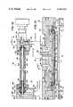
- FIG. 1is a top plan view of a preferred embodiment of the combined CVD/PECVD reactor of the present invention, shown with the cover pivoted open;
- FIG. 2is a vertical cross-section, partly in schematic, taken along line 2--2 in FIG. 1, with the reactor cover closed;
- FIG. 3is a vertical cross-section through the wafer elevator mechanism taken along line 3--3 in FIG. 1;
- FIG. 4-8are sequential, highly schematized representations of the operation of the wafer transport system in positioning wafers within, and removing wafers from the reactor susceptor;
- FIG. 9is a reduced scale, horizontal cross-section through the circular-array, radiant lamp heating assembly, taken along line 9--9 in FIG. 2;
- FIG. 10is an enlarged, partial depiction of FIG. 2 showing the process gas and purge gas distribution systems in greater detail;
- FIG. 11is a partial, enlarged bottom plan view of the gas distribution head or manifold
- FIG. 12depicts an enlarged, vertical cross-section of the RF/gas feed-through system shown in FIG. 2;
- FIGS. 13A-13Cschematically depict various alternative embodiments of the gas feed-through
- FIG. 14illustrates breakdown voltage as a function of pressure for low frequency and high frequency RF power without a constant voltage gradient device
- FIG. 15illustrates breakdown voltage as a function of pressure with and without a constant voltage gradient device
- FIG. 16is a schematic cross-sectional representation of an integrated circuit which illustrates the arrival angles associated with the deposition of a layer of material such as dielectric onto a surface of stepped topography;
- FIGS. 17A and 17Bare schematic cross-sections, similar to FIG. 16, which illustrate the effect of trench width on planarization
- FIGS. 18 and 19are cross-sections of the surface topology of an integrated circuit, in the manner of FIG. 16, illustrating the conformal, planar qualities of oxide films resulting from the application of our planarization process.
- FIGS. 20 and 21depict the deposition rate as a function of temperature and pressure, respectively, for our present oxide deposition process.
- FIGS. 1 and 2are, respectively, a top plan view of the preferred embodiment of the single wafer, reactor 10 of our present invention, shown with the cover pivoted open, and a vertical cross-section of the reactor 10.
- the reactor system 10comprises a housing 12 (also termed a "chamber"), typically made of aluminum, which defines an inner vacuum chamber 13 that has a plasma processing region 14 (FIG. 6.
- the reactor system 10also includes a wafer-holding susceptor 16 and a unique wafer transport system 18 (FIG. 1) that includes vertically movable wafer support fingers 20 and susceptor support fingers 22. These fingers cooperate with an external robotic blade 24 (FIG. 1) for introducing wafers 15 into the process region or chamber 14 and depositing the wafers 15 on the susceptor 16 for processing, then removing the wafers 15 from the susceptor 16 and the chamber 12.
- the reactor system 10further comprises a process/purge gas manifold or "box" 26 that applies process gas and purging gas to the chamber 13, an RF power supply and matching network 28 for creating and sustaining a process gas plasma from the inlet gas and a lamp heating system 30 for heating the susceptor 16 and wafer 15 positioned on the susceptor to effect deposition onto the wafer.
- a process/purge gas manifold or "box” 26that applies process gas and purging gas to the chamber 13
- an RF power supply and matching network 28for creating and sustaining a process gas plasma from the inlet gas
- a lamp heating system 30for heating the susceptor 16 and wafer 15 positioned on the susceptor to effect deposition onto the wafer.
- high frequency RF powerof 13.56 MHz is used, but low frequencies can be used.
- the gas manifold 26is part of a unique process and purge gas distribution system 32 (FIGS. 2 and 10) that is designed to flow the process gas evenly radially outwardly across the wafer 15 to promote even deposition across the wafer and to purge the spent gas and entrained products radially outwardly from the edge of the wafer 15 at both the top and bottom thereof to substantially eliminate deposition on (and within) the gas manifold or box 26 and the chamber 12.
- a unique process and purge gas distribution system 32(FIGS. 2 and 10) that is designed to flow the process gas evenly radially outwardly across the wafer 15 to promote even deposition across the wafer and to purge the spent gas and entrained products radially outwardly from the edge of the wafer 15 at both the top and bottom thereof to substantially eliminate deposition on (and within) the gas manifold or box 26 and the chamber 12.
- a liquid cooling system 34controls the temperature of the components of the chamber 12 including, in particular, the temperature of the gas manifold or box 26.
- the temperature of the gas box componentsis selected to eliminate premature deposition within the gas box/manifold 26 upstream from the process chamber 14.
- the reactor system 10includes a unique, RF/gas feed-through device 36 (FIGS. 2 and 12) that supplies process and purge gas to the RF-driven gas manifold 26 from an electrically ground supply.
- RF energyto the gas box or manifold 26 has the advantage of the wafer residing on the grounded counter electrode or susceptor 16, which makes possible a high degree of plasma confinement that would not be achievable if the RF energy were applied to the wafer and the gas box were grounded.
- the hardwareis mechanically and electrically simpler since electrical isolation between wafer/susceptor and chamber is not required (or permitted). Temperature measurement and control of the susceptor/wafer in the presence of high frequency electric and magnetic fields is greatly simplified with the susceptor 16 grounded.
- the feed-through 36is rigid, eliminating flexible gas connections and the purge gas flow path safely carries any leaking process gas into the chamber to the chamber exhaust.
- the capability to apply RF power to the gas manifoldis made possible (despite the inherent tendency of high potential RF operation to form a deposition plasma within the feed-through) by the unique design of the feed-through, which drops the RF potential evenly along the length of the feed-through, thus preventing a plasma discharge within.
- the wafer transport system 18comprises a plurality of radially-extending wafer-support fingers 20 which are aligned with and spaced about the periphery of susceptor 16 and are mounted to a semi-circular mounting bar or bracket 38.
- an array of radially-extending susceptor-support fingers 22are spaced circumferentially about the susceptor 16, interdigitated with the wafer support fingers 20, and are mounted to a semi-circular bar 40 positioned just outside bar 38.
- the arcuate mounting bars 38 and 40are mounted within a generally semi-circular groove 42 formed in the housing, and are actuated respectively, by vertically movable elevator assemblies 44 and 46.
- the susceptor elevator mechanism 44includes a vertically movable shaft 48 that mounts the bar 38 at the upper end thereof.
- the shaftcan be moved vertically up and down by various moving means 56, including a pneumatic cylinder, or, preferably, a stepper motor operating via suitable gear drive.
- Wafer elevator mechanism 46is similar to the elevator 44.
- FIGS. 4-8The operation of the wafer transport system 18 is summarized by the sequence depicted schematically in FIGS. 4-8.
- the external blade 24(with the wafer 15 to be processed supported thereon) is inserted via opening 56 into chamber 13 to a position over the susceptor 16.
- One example of a suitable blade 24 and associated robot wafer handling system(and door 25, FIG. 6) is described in co-pending, commonly assigned U.S. patent application Ser. No. 944,803, now abandoned, entitled “Multiple Chamber Integrated System”, filed concurrently in the name of Dan Maydan, Sasson Somekh, David N. K. Wang, David Cheng, Masato Toshima, Isaac Harari, and Peter Hoppe which application is hereby incorporated by reference in its entirety.
- the wafer fingers 20--20are positioned between the susceptor 16 and the blade 24.
- the wafer elevator mechanism 44raises the wafer-support fingers 20--20 above the blade 24 to pick up the wafer 15.
- the blade 24is then withdrawn from the chamber 13.
- a pneumatic cylindercloses door 25 over the blade access slot 56 to seal chamber 13.
- the susceptor elevator mechanism 46is actuated to raise the susceptor-support fingers 22 and susceptor 16 so that the susceptor 16 lifts the wafer 15 from the fingers 20--20 into position for processing in the area 14 immediately adjacent the gas distribution manifold 26.
- the spacing, d, between the wafer 15 and manifold 26is readily selected by adjusting the travel of the elevator 46.
- the susceptor fingers 22 and elevator mounting 46maintains the horizontal orientation of the susceptor 16 and wafer 15 and parallelism between the wafer 15 and manifold 26 independent of the spacing, d.
- the susceptor elevator mechanism 46lowers the susceptor fingers 22 and the susceptor 16 to deposit the wafer 15 on the wafer support fingers 20--20.
- the door 25is then opened and blade 24 is again inserted into the chamber 13.
- elevator mechanism 44lowers the wafer-support fingers 20--20 to deposit the wafer 15 on the blade 24.
- the bladeis retracted, leaving the fingers 20 and 22 in the position shown in FIG. 4 preparatory to another wafer insertion, processing and withdrawal cycle.
- the radiant heating system shown in FIGS. 2 and 9provides a reliable, efficient and inexpensive means for heating the circular susceptor 16 and wafer 15 (e.g., silicon) in a manner that provides uniform wafer temperature, accurate absolute wafer temperature and rapid thermal response at low temperatures, preferably ⁇ 600° C.
- a number of requirementsmust be met.
- achieving uniform wafer temperaturerequires compensating the radiation losses at the edge of the wafer.
- high efficiency at low wafer temperatures( ⁇ 600° C.) requires a high emissivity, high thermal conductivity susceptor 16 because silicon wafers have low emissivity at low temperatures in the near-infrared spectrum.
- near-infrared radiationis used to obtain fast heating response and for transmission through the inexpensive materials such as quartz window 70.
- the circular thin susceptor 16is low thermal capacitance for fast heating and cooling response.
- the heating system 30preferably comprises an annular array of small, inexpensive, single-ended vertically oriented lamps 58--58 which provide radiation in the near-infrared portion of the electromagnetic spectrum.
- the lamps 58--58are mounted within an annular circular reflector module 60, preferably of aluminum.
- the module base 60is formed from a block of aluminum, and has a polished annular reflecting channel 62 machined therein.
- the channel 62has an arcuate, generally semi-circular reflecting base 64.
- the module 60 and lamps 58--58are cooled by an annular cooling passage 66 that is formed within the collimating annular reflector 62. Connections are provided for the inlet and outlet of cooling liquid which, typically, is chilled water from a pressurized supply. Power is supplied to the lamp sockets 63 and associated lamps 58 by an electrical supply cable 68, typically from a variable power supply which automatically varies the lamp power based upon a predetermined program setting that is adapted to the requirements of the particular deposition process.
- the annularly-collimated light from the vertical oriented lamps 58--58is admitted into the chamber via a quartz window 70. Quartz is transparent to near-IR radiation.
- the transparent quartz window 70is mounted to the housing 13 at the bottom of the process chamber 13 using annular seals 72--72 to provide a vacuum-tight interface between the window 70 and the housing.
- This mounting arrangementpositions the radiant energy heating source 30 outside the chamber 13 at atmospheric pressure and isolates the vacuum of the processing chamber and the particulate-sensitive processing therein from the lamps.
- a bracket 74can be joined to the lamp mounting base 60 and pivotally mounted by pivot pin 76 to a mating bracket 78, which is joined to the housing 12.
- the lamp modulecan be bolted in place.
- the lamp assemblyis readily accessible for maintenance, lamp replacement, etc., by simply disengaging a clamp 79 to allow the assembly to pivot downwardly about pin 76.
- the lamps 58--58are small single-ended commercially available quartz-tungsten-halogen lamps which provide the required near-infrared radiation.
- One suitable lampis the Ansi type "FEL" supplied by Sylvania, G.E., Ushio or Phillips.
- FELAnsi type
- fourteen 0.5 to 1 kilowatt quartz-tungsten-halogen lamps that provide a wavelength of about 0.9 to 1.5 micronprovide an annularly-collimated power density of up to about 94 W/cm 2 at the top of the lamp module.
- the maximum power density at the susceptor(substantially directed to the outer ⁇ 1.5 in. radius of a 6 in. diameter susceptor) is ⁇ 17 W/cm 2 taking all efficiency into account ( ⁇ 15-16% efficiency).
- lamps concentrating their radiation in the range of about 0.7 to 2.5 microns wavelengthwould be particularly useful.
- the aluminum base 60 and concave-bottom, annular groove 62provide a high collection-efficiency collimating reflector which directs a higher radiation power density at the susceptor edge than at the middle. This non-uniform, concentrated radiation heats the susceptor wafer circumferentially, which compensates the wafer edge heat losses and, thus, provides uniform wafer temperature over a wide range of chamber gas pressures and wafer temperatures.
- the desired uniform radiant wafer heatingis provided by small, inexpensive lamps mounted in a compact simple aluminum module 60 that is easily cooled and maintained at a low temperature, and does not require plating.
- the use of the near-IR lamps and a thin, low mass, low thermal capacity, high emissivity susceptor of material such as graphiteprovides maximum efficiency, fast thermal response, excellent temperature uniformity and transmission through the quartz window 70.
- Other susceptor materialsinclude anodized aluminum, graphite coated with layers such as aluminum oxide (Al 2 O 3 ), or silicon carbide, or a composite ceramic coated with Al 2 O 3 or SiC or other materials.
- interchangeable modules 60 having channels of different heights or diameterscan be used to accommodate different susceptor and wafer diameters.
- a present version of the reactoris designed for 5-6 in. wafers.
- different lamp modulescan be provided for smaller or larger diameter wafers by changing the module height and/or the radius of the module and the filament circle.
- the heating system 30may employ a controller (not shown) such as a closed loop temperature control system using phase angle power control to provide rapid thermal response and rapid wafer temperature stability.
- the simplicity, low mass and high performance characteristics of the heating system 30are in contrast to prior wafer heating approaches which typically use a rectangular array of double-ended quartz-tungsten-halogen lamps.
- Conventional radiation heating practicehas been to use a more massive susceptor and, if excellent temperature uniformity is required, to merely block radiation from the wafer center, thus sacrificing efficiency, rather than redirecting radiation.
- the advantages of the radiant heating system 30 over the conventional practicesinclude in addition to the aforementioned uniform wafer temperature and much faster response time (both heating and cooling), smaller, less bulky more easily maintained equipment of higher reliability (long lamp lifetime); more efficient operation; and lower cost.
- the gas distribution system 32is structured to provide a unique combination of at least four structural features.
- the gas manifold 26is one-half (the powered half) of an electrode pair.
- the powered manifold 26provides high power.
- the gas manifold 26 and other gas distribution surfacesare temperature controlled, which contributes to uniform deposition on the wafer 15 and prevents gas decomposition, deposition or condensation within the gas distribution system upstream from the plasma processing area 14 despite the use of reactant gases such as TEOS which condenses at ⁇ 35° C. and decomposes or reacts with ozone at ⁇ 75° C.
- the external manifold temperatureis controlled, e.g., to >100° C., to prevent the deposition of flaky, particulate-causing deposits.
- the gas manifold 26 and gas distribution system 32provide a clean, uniform deposition process.
- the incorporated circumferential purging gas flowprevents deposition outside of the gas distribution area, i.e., outside the wafer on the internal chamber surfaces and gas distribution system surfaces.
- gas distribution system 32The above features of gas distribution system 32 are depicted most clearly in the FIG. 2 vertical section view and the FIG. 10 enlarged vertical section view.
- the gas manifold 26 and associated distribution systemare part of the housing cover 80, which is pivotably mounted to the housing 12 by pivot means (not shown) to facilitate access to the interior of the housing, including chamber 13, plasma process chamber 14, and associated internal components of the wafer and susceptor elevator mechanisms (44,46).
- the process gas flow from the feed-through 36is directed into the cover 80 by inlet bore 88 which communicates with, that is, feeds into, gas manifold chamber 90 formed by the apertured manifold face plate 92.
- a uniquely designed baffle plate 94is mounted within the gas manifold chamber 90 by means such as standoffs (not shown) to route the process gas around the outside of the edge of the baffle 94 and then radially inwardly along the bottom of the baffle and out the apertures 96--96 in the manifold plate into the plasma processing region 14 above wafer 15.
- the cover 80including the manifold 26 thereof, is heated (or cooled) by an internal flow of fluid or liquid such as de-ionized water along internal path 81 defined by inlet channel 82, annular channel 84 and outlet channel 86.
- this flowkeeps the face plate 92 within the range 100° C.-200° C., in order to ensure that any deposition on the face of the gas manifold which is exposed to the plasma is a hard film. A poor film formed on this surface can create particulates and this must be avoided.
- the flowpreferably holds baffle 94 within the range, most preferably within 35° C.-65° C., to prevent internal deposition or condensation of low vapor pressure process gases such as TEOS and to prevent decomposition and reactions of gases such as TEOS and ozone.
- TEOSlow vapor pressure process gases
- TEOSdecomposition and reactions of gases
- ozoneozone
- De-ionized wateris used because the manifold 26 is the RF powered cathode and de-ionized water is a non-conductor.
- the inlet temperature of the wateris selected as required for a particular deposition process and its associated gas chemistry and/or other parameters in order to maintain both the internal surfaces and the external surfaces of the gas box 90 at desired temperatures.
- the process gas flowis along path 91 defined through inlet bore 88, into manifold chamber 90, radially outwardly to the edge of baffle 94 and around the baffle periphery to the bottom thereof, then radially inwardly between the baffle 94 and the manifold plate 96 and out holes 96--96 into the plasma processing region 14 above the wafer 15.
- the flow path of the deposition gas emerging from holes 96--96is generally radially outwardly across the wafer.
- the small volume of the vacuum process chamber 14 and the high useful chamber pressure range of about 0.5 torr to near-atmospheric pressurealso contribute to the tendency to provide a uniform flow radially outward from the center of the wafer 15 with uniform deposition on the wafer and purging without deposition other than on the wafer.
- the manifold holes 96--96are designed to promote this uniformity of deposition.
- the holes(as well as the manifold temperature, discussed above) are also designed to avoid the formation of deposits on the manifold outer (bottom) surface 97 and, in particular, to prevent the deposition of soft deposits on surface 97 which could flake off and drop onto the wafer during and after processing.
- the hole arrayis one of generally concentric rings of holes 96--96. The distances between adjacent rings (ring-to-ring spacings) are approximately equal, and the hole-to-hole spacing within each ring is approximately equal.
- the patternsare angularly staggered so that no more than two adjacent holes (or some other selected number) are aligned radially. That is, the holes in the gas distribution plate 92 are equally spaced on circles so the hole locations do not form radial straight lines, thereby substantially decreasing deposition on the gas distribution plate itself and enabling uniform gas flow and deposition on the wafer.
- the hole length through the manifold 92i.e., the thickness of the manifold plate 92, and the transverse hole diameter are also selected to promote uniform deposition. Increasing/decreasing the hole length has the effect of decreasing the deposition thickness inside-out/outside-in, as does increasing/decreasing the hole diameter.
- approximately 3400 holes 96--96are used.
- the hole lengthis 0.100 to 0.150 in.
- the hole diameteris 0.028 to 0.035 in.
- the radially asymmetric holesare located on approximately 0.090 in. centers.
- These dimensions and the associated configurationprovide a uniform flow pattern and substantially decrease deposition on the manifold plate 92.
- the present ⁇ 6 in. manifold diameterwill accommodate wafer diameters as large as ⁇ 6 in. Larger wafers can be processed by changing to a larger manifold 26, susceptor 16, larger diameter susceptor 16 and wafer support finger arrays, and by altering the lamp module 30 as described previously.
- a first, upper purge gas flow pathis provided in cover 80 and manifold 26. That is, purge gas flow from the RF/gas feed-through 36 is routed into inlet bore 98 in cover 80 (arrow 93) which feeds into radial channels or grooves 100 that in turn feed into an annular groove 102 formed in the cover concentric with and just above and outside the manifold chamber 90 (arrow 95).
- a ring flow turner 104is mounted concentrically within manifold plate rim 105 and forms a peripheral channel 106 at the inside of the manifold rim that connects the annular channel 102 to the three outer rows of apertures 108 in the manifold plate 92.
- the purge holes 108--108are arranged similarly to the process gas holes 106--106 in generally concentric rings that are spaced at approximately equal ring-to-ring distances.
- the within-ring hole spacingis selected so that the locations of the purge holes 108--108 form staggered radial lines, i.e., so that no two adjacent purge holes are along a radial line.
- the gasis distributed from about 600 holes and the following purge hole dimensions are used: between-ring spacing 0.090 in.; hole diameter 0.025 in.; and hole length 0.040 in.
- a second, lower purge flow path 101, 103, 105is provided via inlet bore 110, formed in the side of the housing 12, which connects or feeds into an annular channel 112 formed generally concentrically about the lower section of the process chamber 13 just above the quartz window 70.
- the channel 112has holes that are spaced about the lower region of the chamber 13 or equivalent yielding feature to feed the lower purge gas uniformly across the quartz window 70 (see arrows 103), around the lower edge of the wafer 15 (arrows 105) and across horizontal quartz cover plate 114, which surrounds the chamber 13 just below the wafer processing chamber 14.
- the plate 114contains an annular pattern of holes 116 therein which are aligned with an annular gas outlet channel 118.
- This channelis connected via outlet bore 121 to a conventional vacuum pumping system (not shown), which establishes the vacuum within the chamber and exhausts the spent gases and entrained gas products from the chamber.
- the upper purge gas flowis through inlet 98 (arrow 93), channels 100, 102 and 106 (arrow 95), then out purge ring apertures 108--108 (arrow 93) at the outer upper edge of the process-positioned wafer 15.
- the lower purge gas flowis through inlet 110 (arrow 101) and annular ring 112 across the quartz window 70, sweeping the window clean (arrow 103), then upwardly toward the lower peripheral bottom edge of the wafer 15 (arrow 105).
- the upper and lower gas purge flows 97 and 105merge at the wafer's edge and flow outwardly as indicated by arrow 107 across the plate 114 and through the holes 116 therein into the annular exhaust channel 118 and out of the chamber along path 109 (FIG. 2).
- This upper and lower, merging flow patternnot only keeps the quartz window 70 clean, but also sweeps spent deposition gases, entrained particulates, etc., out of the chamber 13.
- the combination of the dual, upper and lower purge flowswhich are conformed to the inner quartz window chamber surfaces and to the circumferential wafer edge and the very high chamber pressures (unusually high for PECVD) provide a very effective purge and prevent deposition external to the wafer.
- Equally important, uniform radial gas flowis provided across the wafer 15 by the multiplicity of holes 116--116, illustratively five in number, which are formed in the distributor plate 114 peripherally around the wafer 15. These holes 116 communicate into the larger semi-circular exhaust channel 118 which, in turn, is connected to the vacuum exhaust pumping system via the single outlet connection 121.
- the channel 118has large conductance relative to the holes 116--116 because of its relatively very large volume, which provides uniform pumping at all points radially from the wafer, with the simplicity of a single point pump connection.
- this uniform radial pumpingprovides uniform gas flow across the wafer 15 at all pressures and, thus, uniform deposition even at very high chamber pressures such as 200 torr and above.
- manifold 26is usable as an electrode for a uniform glow discharge plasma at unusually high pressures, which enables both the very high deposition rate and the effective purge flow.
- the advantages of using the gas box 26 as the powered RF electrodeinclude the wafer residing on the grounded counter electrode, which makes possible a high degree of plasma confinement that would not be achievable if the RF energy was applied to the wafer and the gas box was grounded. Additionally, the hardware is mechanically and electrically simpler since electrical isolation between wafer/susceptor and chamber is not required (or permitted). Temperature measurement and control of the susceptor/wafer in the presence of high frequency electric and magnetic fields is greatly simplified with the susceptor grounded.
- Our combination RF/gas feed-through 36(FIG. 12) is designed to apply RF power to the gas box 26, that is, to use the gas box as the powered RF electrode, without breakdown of the process gas and without deposition within the gas distribution system.
- the RF/gas feed-through 36is of a compact, low profile design, despite our design objective that the high RF potential be applied parallel to the gas flow path to yield a constant voltage gradient over a distance to eliminate the high local electric field which causes electrical breakdown.
- the first approachflows the gas within an insulating tube between surfaces that are at a high electric potential difference.
- a second approachflows the process gas through an insulator between the surfaces of high electric potential difference at sufficiently high gas pressure so that electrical breakdown does not occur.
- the first approachis not compact and does not work at high frequencies, where electrical breakdown is more efficient (see, e.g., curve 201 and 200, FIG. 14). Also, this first approach is not capable of operation where there is a small p.d (pressure.distance) product.
- the second approachis more compact than the first, and less susceptible to electrical breakdown at high frequencies, but is also subject to electrical breakdown where there is a small pressure.distance product.
- the feed-through 36comprises an inlet end connector or manifold 120, an outlet end connector or manifold 122 and an intermediate gas feed structure 124 comprising a quartz tube 126 and an elongated insulating transition housing 128.
- the block 128is mounted to and between the end connectors 120 and 122 using O-ring seals 130--130 to provide vacuum-tight mounting.
- the internal bore 127 of the quartz tube 126communicates with gas inlet bore 134 in the inlet end connector and gas outlet bore 136 in the outlet end connector.
- Process gases and purge gas under pressure from sources such as an ozone generator, a liquid-TEOS vaporizer, and conventional pressurized gas tanks or bottlesare routed through conventional valves or an automatic flow control system for controlled flow rate application to the inlet manifold 120.
- process gasis routed through the feed-through device 36 via the inlet bore 134 and through the quartz tube 126 and out the outlet bore 136 and into the mating inlet bore 88 in the gas distribution head 32.
- the feed-throughis shown enlarged in FIG. 12 to facilitate illustration.
- the actual feed-through 36is of a size so that the gas outlets 136 and 146 are aligned with the mating channels or bores 88 and 98 in the reactor cover 80.
- the purge gasesare routed through the feed-through co-axially with the process gas flow path so that if there is a leak along the process gas path 131-133-135, the process gas is harmlessly transported into the process chamber 14 along with the purge gas and, thus, does not escape into the ambient.
- the incoming purge gasis applied to inlet bore 138 in the inlet end connector 120.
- Bore 138communicates with an annular channel 139 formed in the spool-shaped fitting 140 which is mounted near the inlet end of the quartz tube 126.
- This spool fitting 140is sealed at the outer end thereof by cylindrical flange fitting 142 and O-ring seal 144.
- the annular channel 139communicates via holes (not shown) with the annular passage 147 between the tube 126 and concentric block 128.
- the passageway 147feeds similarly into annular chamber 139 in fitting 140 at the outlet end of the tube 126.
- the tube 126is mounted and sealed at the outlet in the same way described above relative to its inlet end.
- chamber 139feeds into the outlet bore 136.
- This arrangementprovides an isolated purge gas flow path through the feed-through 36, as indicated by arrows 148-156.
- the co-axial gas feed apparatus described aboveprovides a dual barrier which prevents the leakage of potentially toxic process gases into the atmosphere. That is, the path to the ambient between mating surfaces is barred by the two sets of O-ring seals 130 and 144. These seals are positioned in series along the potential path to the ambient. Also, as mentioned, in the event of internal system leaks such as a leak in the quartz tube 126, the purge gas flow carries the process gas into the process chamber 14, where both are exhausted by the chamber vacuum system. In addition, the process and purge gases are routed entirely through the chamber components, i.e., through substantial blocks/bodies such as the aluminum connectors 120 and 122 and the insulator block 128. Consequently, external, typically flexible, gas tubing is eliminated at the reactor. The very solid, secure routing fixtures, the dual seal barriers, and the co-axial gas flow in which the purge gas flow surrounds the process gas flow, provide a safe, secure process gas flow path in the reactor and feed-through device.
- the inlet end connector 120is connected to ground.
- the outlet end connector 122is connected to the RF power supply 128 and connects the RF energy to the cover 80 and manifold plate 92.
- a constant electric potential gradientis provided along the column of process gas flow between the grounded connector 120 and the driven connector 122 by providing one of three types of constant voltage gradient elements along the surface of the quartz insulating tube 26: a radio frequency coil which provides resistive, inductive, or capacitive (effective) impedance; a resistive film; or a resistive sleeve.
- the RF coil 160is a wire coil that is wound around the quartz gas tube 26 between the ends thereof and the high voltage which is applied across the tube length.
- the wire coil 160is of No. 24 to No. 26 AWG aluminum wire.
- the desired electrical impedance at the frequency of operationis obtained by selecting the wire material, diameter, number of turns per unit length, length and the winding technique.
- This A.C. impedancecan be selected to have a net inductive/resistive impedance or a net capacitive/resistive impedance or to be purely resistive (resonant).
- the A.C. and D.C. resistancecan be selected (using wire diameter, length, and material).
- a typical applicationhas a high inductive reactance but is a D.C. short.
- typical values for the inductance of an RF coil-type feed-throughare approximately 10-15 microHenries.
- a resistance of 100 to 500 Kohmsis typical.
- a resistive film 162 of material of controlled electrical resistivity and thicknesssuch as Acheson "Aerodag G” (a colloidal suspension of micron size graphite particles in an isopropyl alcohol dispersing medium), is coated on the outside of the quartz tube 126 to provide the desired resistive impedance and allow broad band (frequency) operation.
- Acheson "Aerodag G”a colloidal suspension of micron size graphite particles in an isopropyl alcohol dispersing medium
- the third alternative shown in FIG. 13Cuses a solid resistive sleeve 164 of a material such as a composite ceramic of controlled electrical resistivity, to provide the desired electrical resistive impedance and broad band frequency operation.
- a variant of the solid resistive sleeve 164uses a sleeve of material which is ferromagnetic with very high permeability at the frequency of interest, and has controlled electrical resistivity. Operation is the same as for the resistive sleeve 164, with this added advantage. Should breakdown occur under severe conditions, the presence of magnetic material and initially high current and resulting high magnetic field produces a very large inductive reactance to charge flux (current), which very quickly reduces then extinguishes electrical conduction in the process gas.
- FIG. 14illustrates representative bench test data for a quartz tube without a constant voltage gradient device of voltage breakdown in kilovolts as a function of pressure in torr at both low (100 kHz) and high (13.56 MHz) radio frequencies. As indicated, for the pressure range of 5-20 torr, the breakdown range was 3 to 7 kV for the low radio frequency and approximately 2 to 5 kV for the high radio frequency.
- FIG. 15illustrates bench test data of breakdown voltage as a function of pressure for Tube A, a tube of length 10.5 cm and diameter 0.6 cm without a constant voltage gradient device, and Tube B, the same tube with a constant voltage gradient device of the wire coil type, 160, consisting of 160 turns of ⁇ 26 AWG wire.
- Tube Cwas the same as tube B, except for having a greater length, 13.4 cm.
- This illustrates that the RF/gas feed-through 36is very effective in preventing breakdown and subsequent deposition of process gases under actual reactor operating conditions.
- the reactor system 10will be used at pressures of up to 200 torr and above, at which values the breakdown voltages will be much higher than those depicted in FIG. 14.
- the anti-electrical breakdown gas feed-through 36 of the present inventionprovides a constant voltage gradient along the process gas flow column, without charge build-up.
- the feed-through 36is designed to incorporate resistive, inductive or capacitive electrical impedance between the high potential difference ground and driven surfaces. The choice of impedance depends upon the electrical requirements of the system, i.e., low frequency, high frequency, wide band, d.c. operation, etc. This constant electrical potential gradient effectively prevents premature breakdown and deposition within the gas distribution system 32 and feed-through 36 at high or low radio frequencies.
- the structure of the feed-through 36 including the co-axial gas feedis highly resistant to process gas leaks and purges any process gas leaks into the system exhaust.
- temperature controlled watercan be flowed through channels (not shown) in the feed-through device 36 isolated from process and purge channels to (heat or cool) control the temperature of the gas in the feed-through.
- gasessuch as ozone or TEOS
- Our reactoruses a tailored non-uniform near-IR radiant heating pattern and a thin, low mass high emissivity susceptor to provide thermal efficiency, fast thermal response (heating and cooling), excellent temperature uniformity despite the inherent non-uniform heat losses of thin circular wafers, and good transmission through a chamber window of quartz or the like (which permits external mounting of the radiant heating module).
- the RF powered gas manifold 26provides the necessary high power to enable confinement of the plasma.
- the uniform gas inlet flow pattern provided by the gas manifold and radial exhaust pumpingprovide uniform gas inlet and exhaust (purge) pumping and uniform radially gas flow across the wafer, enabling uniform processing (deposition/etching) over a wide pressure regime including very high pressures.
- the radial pumping and high pressure capabilityprovide confinement of the plasma/reactant species to the wafer and; in enabling effective purging, prevent deposition within the chamber except on the wafer.
- the precisely temperature-controlled internal and external surfaces of the gas manifoldprevent decomposition, reactions, condensation, etc., within the gas box and eliminate undesirable particulate-generating deposits on the external gas box surfaces.
- temperature controlled wateris circulated within the gas box to maintain the temperature between about 35° C.-75° C. to prevent internal deposition or condensation of TEOS below about 35° C. and to prevent internal decomposition of or reaction between ozone and TEOS above about 70° C., and to maintain the external face of the gas manifold greater than about 100 ° C. to prevent flaky external deposits.
- the gas feed-throughprovides the enables the application of high voltage RF power to the gas box, as well as the application of purge gas and process gas to the gas box, without gas breakdown.
- a one-axis robot susceptor/wafer support and transport systemis adapted to load and unload wafers at a selected position within the chamber onto and from an external robot blade.
- This transport systemprovides variable parallel close-spacing between the susceptor/wafer and the overlying gas manifold and provides variable spacing by simply selecting the vertical travel of the associated susceptor support fingers and susceptor elevator mechanism.
- the parallelismincreases plasma stability and uniformity by eliminating the tendency to run to one side or the other and, thus, enables uniform processing (deposition and etching).
- the variable close spacing manifold and the wafer surfacefacilitate the implementation of different types of process.
- the spacingcan be set at a very small variable dimension such as, for example, one centimeter, 0.5 centimeter and even smaller, to enable confinement of the plasma and/or gaseous reactants between the gas distributor and the wafer. This confinement increases the reaction efficiency and increases the rate of the reaction (deposition or etching) and helps prevent deposition everywhere except on the wafer, and even at very high chamber pressures.
- High pressure capabilityresults from a number of the above-summarized factors including uniform radial pumping, the uniform gas flow provided by the gas manifold, the confinement provided by the variable close spacing between the electrodes and the application of high power density RF power to the gas manifold.
- Temperature control of the gas box external surface to >100° C.is important to prevent the deposition of porous particulate causing films.
- High pressure operationincreases ion scattering, which decreases bombardment of and damage to the wafer and enhances step coverage. This, because high pressure operation dilutes the concentration of the gas molecules to the point where they do not react at a sufficient rate to cause particles/unwanted deposition on surfaces.
- the high pressure capability and associated decreased bombardmentenables one to decrease the bombardment level for a given power/voltage and reaction rate or, alternatively, to use higher power/voltage to obtain a higher reaction rate for a given bombardment level.
- Uniform flow distributionis also critical, particularly at the close spacing of less than one centimeter used in our reactor, because it confines the plasma and thus enhances clean operation.
- the ability to adjust the electrode spacing with parallelismpermits the use of the close spacing with the plasma stability necessary for deposition.
- variable large spacing in combination with the high pressure capabilitypermits effective etchback.
- the variable spacing between electrodesis very important because it would be impossible to optimize the etch and other processes without varying the electrode spacing used for deposition. For example, a typical spacing of ⁇ 1 cm is used for thermal CVD and PECVD while the etchback requires a spacing of ⁇ 0.4 in. or 1 cm.
- variable spacingin combination with variable pressure permits effective reactor self-cleaning.
- the required spacing, d, ⁇ 0.4 in. or 1 cm.is larger than that required for, e.g., thermal CVD and PECVD.
- the relatively larger spacing and wide pressure regimepermits the plasma to diffuse within the reactor (rather than being confined as required for the deposition processes) and clean the entire reactor.
- a typical self-cleaning sequenceuses RF power of 500 watts, gas NF 3 or other fluorine containing chemistry at flow rates typically of 0.1 slm, pressure of 0.5 torr, and d ⁇ 0.4 in., and has provided ebb rates of .sup. ⁇ 0.5 micron/sum.
- the high pressure capability combined with 0.2 in. spacing as well as the ability to apply RF power to the gas box at high power levelspermits sputtering of materials such as oxide or other drelectrics using gas chemistry such as argon or other heavy molecule gas chemistry such as SiCl 4 .
- a typical sputtering processinvolves application of RF power of 700 watts, gas flow rates 0.1 slm, pressure of 10 mt. electrode spacing, d, of 0.2 in. to 0.5 in.
- the processing steps and multiple step processing sequences described herewere performed in the reactor 10.
- the ability to perform multiple step processing using temperature sensitive gases such as ozone and TEOS and different steps such as CVD, PECVD, etching, and self-cleaning in-situqualifies the reactor 10 as being uniquely preferred.
- temperature sensitive gasessuch as ozone and TEOS
- different stepssuch as CVD, PECVD, etching, and self-cleaning in-situ qualifies the reactor 10 as being uniquely preferred.
- the process disclosure herewill permit those of usual skill in the art to practice the process sequences albeit in single process, dedicated reactors and to adapt such reactors, e.g, to the use of the process.
- the thermal chemical vapor deposition of highly conformal silicon dioxideis an improvement of methods which use the pyrolysis of TEOS and oxygen.
- the present thermal CVD inventionis based in part upon the discovery that improved highly conformal ( ⁇ 100%) silicon dioxide coatings are formed by the thermal chemical vapor deposition of the reactants TEOS and ozone at relatively low temperatures, using lamp radiant heating to provide a wafer temperature of about 200° ° C.-500° C., and high pressures.
- the ozonelowers the activation energy of the reaction kinetics and forms silicon dioxide with the TEOS at the relatively low temperatures of about 200° C. to 500° C.
- a commercially available high pressure, corona discharge ozone generatoris used to supply a mixture of (4-8) weight percent ozone in oxygen to the gas distributor.
- Helium carrier gasis bubbled through liquid TEOS to vaporize the TEOS and supply the diluted gaseous TEOS in the He carrier to the gas distributor.
- the thermal chemical vapor deposition processuses the reactants ozone (O 3 ), oxygen and tetraethylorthosilicate (TEOS) at a low temperature within the range of about 200° C.-500° C. and at a high pressure within the range of about 10-200 torr and, preferably about 40-120 torr, to deposit a highly conformal silicon dioxide coating that fills in the voids, cusps and other topographical irregularities and thereby provide a substantially planar surface.
- ozoneO 3
- oxygen and tetraethylorthosilicate (TEOS)at a low temperature within the range of about 200° C.-500° C. and at a high pressure within the range of about 10-200 torr and, preferably about 40-120 torr, to deposit a highly conformal silicon dioxide coating that fills in the voids, cusps and other topographical irregularities and thereby provide a substantially planar surface.
- TEOStetraethylor
- the ozoneis applied at a flow rate of 2 to 3 slm
- the helium carrier gas flow rateis 50 sccm to 1.5 slm
- the chamber pressureis 40 to 120 torr
- the wafer temperatureis 375° C. ⁇ 20° C., thereby providing a highly conformal undoped silicon dioxide coating at a deposition rate of 3,000 Angstroms/min.
- the gas distribution manifold (gas distributor 26) of the reactor 10is controlled by de-ionized water of temperature 20-50° C. circulating in passages therein to maintain the internal surface of the gas distributor 26 within the narrow range of about 35° C.-75° C., i.e., at a temperature of less than about 75° C. to prevent decomposition of the TEOS and reaction between the TEOS and ozone and above 35° C. to prevent condensation of the TEOS inside the gas distributor.
- the distance, d, from the temperature-controlled gas distributor to the surface of the substrateis preferably approximately one centimeter or less. This distance of one centimeter or less confines the plasma or gaseous reactants between the gas distribution 26 and the wafer 15. This increases the reaction efficiency, and increases the rate of the reaction (deposition) and helps to prevent deposition everywhere except on the wafer.
- the thermal CVD process of the present inventionuses unusually high deposition chamber pressures: pressures of preferably at least ⁇ 10 torr and of about 20-200 torr are utilized. Even the lower portion of this range is over 20 times greater than the total pressure normally utilized in processes utilizing TEOS.
- the high pressureincreases the density of available reactive species and, thus, provides a high deposition rate.
- the use of high pressureenables an effective purge.
- the high purge flow rateimproves the ability to remove waste gases, entrained particulates, etc., without unwanted deposition on the chamber surfaces.
- the above-described bottom purge flowsweeps radially outwardly across the bottom side of the susceptor wafer.
- the bottom flowis joined by an upper purge flow that is directed downwardly at the wafer's periphery.
- the combined streamsflow radially outwardly from the periphery of the wafer, and cause the deposition gas to flow radially uniformly outwardly, then through the exhaust system of the chamber at very high flow rates.
- useful top purge gas flow rate(preferably nitrogen) may be from 1 slm to 10 slm and the bottom purge gas flow rate (again, nitrogen) may be 1 slm to 20 slm.
- the above-described gas flow, chamber pressure, and resulting chamber temperaturehave provided a silicon dioxide deposition rate of about 500 Angstroms/min. to 4,000 Angstroms/min.
- the deposition ratepeaks at about 375° C. ⁇ 20° C.
- the decreased deposition above and below the peakis a consequence of unfavorable reaction kinetics at the surface of the substrate.
- the peak temperatureis also close to the maximum processing temperature of about 400° C. for aluminum-containing multiple conductor structures. Above ⁇ 400° C., hillocks form in aluminum. Above -500° C., aluminum softens.
- the deposition ratesaturates at 3,000 Angstroms/min. at a chamber pressure of 80 torr, and wafer surface temperature of 375° C. (using a TEOS temperature of 35° C.), with very little increase at higher pressures. Decreasing the temperature to 200°-375° C. at 80 torr decreases the deposition rate to 1,000-3,000 Angstroms/min., respectively. At 20 torr, temperatures of 200°-375° C. provide a deposition rate of 500-1000 Angstroms/min. Above pressures of about 120 torr, gas phase reactions increase particulates. This can be controlled by decreasing the wafer temperature or increasing the diluent flow rate, but these steps decrease the deposition rate.
- the resulting filmshave been characterized as having improved physical and electrical properties such as cracking resistance, density, refractive index, shrinkage, rate of etching, breakdown voltage, flat band voltage, mobile ion contamination, pin hole density and silicon oxide purities, the crucial aspect is the excellent ⁇ 100% conformal coverage over vertical and horizontal surfaces of steps and over other surface irregularities. Consequently, problems such as overhang, cusps and voids are much less severe, thereby minimizing or even eliminating the amount of follow-up processing which must be done to remedy such problems and to achieve planarization.
- the conformal oxidecould be doped to a low level of, e.g., 1 weight percent to 10 weight percent of phosphorus and/or boron by incorporating reactants such as TMP (tetramethylphosphite) and/or TMB (tetramethylborate).
- reactantssuch as TMP (tetramethylphosphite) and/or TMB (tetramethylborate).
- TMPtetramethylphosphite
- TMBtetramethylborate
- the process of the present inventionis an improvement of conventional methods for planarizing silicon dioxides such as, for example, conventional methods using spin-on glass and polyimide deposition with etch-back.
- Another aspect of the present inventionis the use of the above-described thermal CVD silicon dioxide deposition process to substantially planarize a dielectric layer, followed by the use of an isotropic wet or dry etch, preferably at a high etch rate, to complete the planarization process.
- the combination of the above-described low temperature, thermal CVD, conformal oxide deposition process in conjunction with various wet or dry isotropic etch stepsprovides an unexpectedly conformal, planarized dielectric layer which serves well in the small geometry, multi-level metallization structures that are currently being developed and will be developed in the future. Described below is a presently preferred dry isotropic etch process which can be performed in-situ, in the same, referenced multi-step chamber.
- the present inventionis embodied in a three-step process which, first, forms a layer of silicon dioxide, preferably at a high deposition rate; the above-described ozone and TEOS-based thermal CVD conformal oxide deposition process is used as the second step to form a highly conformal oxide coating; then, in the third step, a preferably high rate isotropic etch is applied to quickly complete the planarization process.
- the above-described thermal CVD, conformal oxide deposition processis used in a three-step high deposition rate, high throughput planarization process in-situ in the referenced multiple process CVD/PECVD deposition chamber.
- the planarization processcan be applied over existing dielectric layers or can be used alone to form a planar dielectric.
- the preferred first stepis a PECVD oxide deposition.
- the PECVD oxide deposition processuses a plasma formed from TEOS, oxygen, and a carrier gas with or without a diluent such as helium. This process uses a deposition chamber pressure of from about 1 torr to about 50 torr; an oxygen flow rate of from about 100 sccm to 1,000 sccm, an inert carrier gas (helium) flow rate of from 100 to 1,500 sccm, a total gas flow rate (not including the purge gases) of 200 sccm to 2.5 liters per minute, and RF power to the ⁇ 6 in. diameter gas distributor cathode of about 200-400 watts.
- Power density at the gas distributor/cathode 26is about 1 watt/cm 2 based on calculations for a quasi-parallel plate configuration. Radiant energy is directed to the susceptor from below by the annular array of vertical lamps to generate a deposition plasma and heat the wafer surface to a temperature of 300° to 500° C. Top (nitrogen plus helium mixture) and bottom (nitrogen only) purge gas flow rates of 1 to 15 slm and 1 to 20 slm, respectively, are used with respective preferred top and bottom purge gas flow rates of 2.5 slm and 10 slm. These parameters provide SiO 2 deposition rates of about 5,000 Angstroms/min. to 10,000 Angstroms/min. typically, 0.4 cm 23 d.sup. ⁇ 1 cm.
- Presently preferred operating parameters for the PECVD oxide deposition step for a 6 in. waferare 600 sccm oxygen, 900 sccm helium, 16,000 sccm total flow (including purge; 1,500 sccm excluding the purge), 10 ⁇ 2 torr pressure and 375° C. ⁇ 20° C. wafer temperature.
- the parametersprovide SiO 2 deposition rates of about 8,500 Angstroms/min. for a gas distributor-to-wafer surface distance, d 167 0.4 cm.
- the above-described high pressure, PECVD oxide deposition processwhich is based upon TEOS gas chemistry and has essentially the same chamber requirements as the crucial conformal silicon dioxide deposition step, makes the use of the same chamber not only possible, but preferable.
- TEOStetraethylorthosilicate
- This pyrolysis processmay be utilized, with a silicon nitride, silane and ammonia plasma, or with an oxynitride, silane, ammonia and N 2 0 plasma.
- Plasma-assisted chemical vapor depositions using TEOS at pressures below 1 Torrare also utilized, with variations including use of spin on glass, and polyimides.
- the present PECVD processprovides methods for improving deposition rate, cracking resistance, physical and electrical properties of CVD-deposited silicon dioxide.
- the present inventionalso provides an improved method for depositing silicon dioxide whereby improved step coverage and lower stress of the deposited layer are obtained.
- the present PECVD processprovides an improved method for the plasma-enhanced chemical vapor deposition of TEOS to obtain the above advantageous improvements whereby the preferred conditions of deposition are a higher than usual pressures (up to 50 Torr) and at temperatures of about 200° to 400° C.
- the usual conditions for the plasma-enhanced chemical vapor deposition using TEOSare at a total pressure range of up to about 1 Torr (including the carrier gas), of which the oxygen in the plasma is at a pressure of about 0.4 Torr.
- the substrate temperatureusually gradually increases from about room temperature to about 400° C. See, for example, Mackens et al., Thin Solid Films, 97:53-61 (1982).
- the deposited silicon dioxide coatings according to the present inventionalso have improved cracking resistance and have improved step coverage over silicon dioxide coatings deposited by other methods.
- the problem of step coveragedeals with the creation of a mushroom-shaped deposited overhang at the corners of the step substrate. This overhang must be remove by subsequent processing, thus complicating the process.
- the problem of the overhangis much less severe, thereby minimizing or even eliminating the amount of processing to remedy this problem.
- the silicon dioxide coatings formed according to the present inventionalso exhibit lower stress and are characterized generally by indices of -IE9 (compression) to +IE9 (tension), with the preferred index being -IE8 Also, the coatings according to the present invention exhibit improved physical and electrical properties and that the density, refractive index, shrinkage parameters, rate of etching, breakdown voltages, flat band voltages, mobile ion contamination, pinhole densities and silicon oxide purity are improved.
- the operation at high pressuresallows the plasma to be confined at the top of the substrate, thus making it less likely to contaminate the sides of the chamber and the surfaces on which deposits are not desired.
- the third stepis a high rate isotropic etch process comprising the step of exposing the existing silicon dioxide surface to a plasma formed from fluorinate gas selected from CF 4 , NF 3 and C 2 F 6 in a doping gas such as helium to stabilize the plasma, in a chamber at a temperature in the range of about 100° C. to 500° C. and preferably 200° C. to 400° C. (Helium and/or oxygen can be incorporated to form gases with the carbon.)
- the total gas chamber pressure for these gaseswill usefully be in the range of about 200 mt to 20 torr.
- the preferred rangeis 500 mt to 10 torr.
- the total gas flow rate of the plasmawill be determinable by those skilled in the art.
- the preferred total gas flow rateis from about 170 sccm to 1.25 slm.
- the useful range for the NF 3 (or C 2 F 6 gas flowis from about 10 sccm to 500 sccm, with the preferred range being from about 70 to 200 sccm.
- the individual flow rate of the doping gas, usually helium,will be from about 10 sccm to 3.5 slm and, preferably, 100 sccm to 1 slm.
- RF power densityof about 0.5-1 watts/cm 2 was used, along with radiant power from the lamp module to provide the substrate temperature of ⁇ 500° C. and the preferred temperature of 200° C.-400° C.
- a distance d ⁇ 0.4 cmis used. Below 0.4 cm, plasma instability increases. Also, as d is increased above 1 cm, the etch may become too effective and etch other components.
- this isotropic etch processis also useful generally, for example, for forming metal contacts, it is particularly useful for providing profile control of SiO 2 step-coverage layers, as described above, .
- this uniform high rate isotropic etchhas the advantage of additionally planarizing the substantially planarized contour which results from the SiO 2 deposition.
- This high rate isotropic etch stepwas done in-situ in the same reactor used for the two above-described silicon dioxide deposition steps.
- this preferred sequenceprovides an integrated in-situ three-step process for forming a planarized silicon dioxide layer even over non-planar layers incorporating small geometry steps, trenches, etc.
- the use of the high rate PECVD oxide deposition step and the high rate etching stepthe ability to use the same chamber for all three steps provides a fast, high throughput planarization process which is also less susceptible to contamination and wafer damage and other problems which result when a wafer is handled repeatedly and switched from one chamber to another.
- FIGS. 18 and 19The use of the above-described three-step planarization process is shown schematically in FIGS. 18 and 19.
- the first stepforms a relatively thick stepped layer 182 of silicon dioxide over the stepped topography 181 at a very high deposition rate.
- the second stepis then used to form thereon conformal silicon dioxide layer 183, which is substantially planarized despite the underlying deep step 184.
- the third, isotropic etch stepquickly etches away the upper surface 185 to below the residual step topography 186, if any, in layer 183, thereby providing a smooth planar surface 187 for subsequent layers.
- the ozone- and TEOS-based thermal CVD stepcan be used in combination with other initial dielectric coatings and other isotropic etch steps.
- the ozone thermal CVD second stepcan be used to deposit a highly conformal silicon dioxide coating on silicon oxide or silicon nitride or silicon oxynitride or other dielectric layers formed by CVD or by other methods, and the resulting substantially planarized layer can be etched to a planar topography using other, preferably high rate, dry (e.g., plasma) or wet chemical isotropic etch methods.
- An isotropic chamber self-cleaning etch sequencehas been done using fluorinated gas at a pressure of about 600 mT to 10 torr, high RF power density of 1-2 watts/cm 2 , distance, d, ⁇ 1 cm and the other parameters, including the gas flow rates, described above for the isotropic etch process.
- This processhas been used to clean the referenced multi-step CVD/PECVD reactor. After depositing an ⁇ 5 ⁇ thick silicon dioxide film on a wafer, the chamber can be cleaned in about one minute.
- the thermal CVD conformal-oxide deposition process using ozone, oxygen and TEOScan be used alone to planarize an existing dielectric which has been formed, for example, without perfect step coverage or with perfect step coverage on a non-perfect topography.
- the conformal oxide-forming thermal CVD stepcan be applied to existing dielectrics followed by an isotropic etch step to etch back any remaining non-planarities to a planar topography.
- the above-described high rate PECVD oxide stepis applied followed by the conformal oxide-forming thermal CVD sequence.
- the high rate PECVD oxide deposition sequenceis utilized followed by the conformal oxide-forming thermal CVD step followed by an isotropic etch step, preferably the above-described high rate plasma isotropic etch.
- the first two steps of the following sequencecan be used to planarize the stepped topography followed by application of the high rate oxide deposition to build up the very thick oxide thickness over the planar surface:
- the very thick planar oxide process described immediately abovecan incorporate an isotropic etch back as the final step to achieve full planarization, and the required thickness.
- the isotropic chamber self-cleaning etchcan be inserted as desired within or at the end of the other process sequences to maintain the chamber in a clean deposition-free state.
Landscapes
- Chemical & Material Sciences (AREA)
- Engineering & Computer Science (AREA)
- Chemical Kinetics & Catalysis (AREA)
- General Chemical & Material Sciences (AREA)
- Materials Engineering (AREA)
- Mechanical Engineering (AREA)
- Metallurgy (AREA)
- Organic Chemistry (AREA)
- Physics & Mathematics (AREA)
- Plasma & Fusion (AREA)
- Analytical Chemistry (AREA)
- Inorganic Chemistry (AREA)
- General Physics & Mathematics (AREA)
- Manufacturing & Machinery (AREA)
- Computer Hardware Design (AREA)
- Microelectronics & Electronic Packaging (AREA)
- Power Engineering (AREA)
- Condensed Matter Physics & Semiconductors (AREA)
- Chemical Vapour Deposition (AREA)
- Crystals, And After-Treatments Of Crystals (AREA)
- Formation Of Insulating Films (AREA)
- Drying Of Semiconductors (AREA)
- Container, Conveyance, Adherence, Positioning, Of Wafer (AREA)
- ing And Chemical Polishing (AREA)
- Silicon Compounds (AREA)
Abstract
Description
The present invention relates to a reactor and methods for performing single and in-situ multiple integrated circuit processing steps, including thermal CVD, plasma-enhanced chemical vapor deposition (PECVD), reactor self-cleaning, film etchback, and modification of profile or other film property by sputtering. The present invention also relates to a process for forming conformal, planar dielectric layers on integrated circuit wafers and to an in-situ multi-step process for forming conformal, planar dielectric layers that are suitable for use as interlevel dielectrics for multi-layer metallization interconnects.
The early gas chemistry deposition reactors that were applied to semiconductor integrated circuit fabrication used relatively high temperature, thermally-activated chemistry to deposit from a gas onto a heated substrate. Such chemical vapor deposition of a solid onto a surface involves a heterogeneous surface reaction of gaseous species that adsorb onto the surface. The rate of film growth and the film quality depend on the wafer surface temperature and on the gaseous species available.
More recently, low temperature plasma-enhanced deposition and etching techniques have been developed for forming diverse materials, including metals such as aluminum and tungsten, dielectric films such as silicon nitride and silicon dioxide, and semiconductor films such as silicon.
The plasma used in the available plasma-enhanced chemical vapor deposition processes is a low pressure reactant gas discharge which is developed in an RF field. The plasma is, by definition, an electrically neutral ionized gas in which there are equal number densities of electrons and ions. At the relatively low pressures used in PECVD, the discharge is in the "glow" region and the electron energies can be quite high relative to heavy particle energies. The very high electron temperatures increase the density of disassociated species within the plasma which are available for deposition on nearby surfaces (such as substrates). The enhanced supply of reactive free radicals in the PECVD processes makes possible the deposition of dense, good quality films at lower temperatures and at faster deposition rates (300-400 Angstroms per minute) than are typically possible using purely thermally-activated CVD processes (100-200 Angstroms per minute). However, the deposition rates available using conventional plasma-enhanced processes are still relatively low. Presently, batch-type reactors are used in most commercial PECVD applications. The batch reactors process a relatively large number of wafers at once and, thus, provide relatively high throughput despite the low deposition rates. However, single-wafer reactors have certain advantages, such as the lack of within-batch uniformity problems, which make such reactors attractive, particularly for large, expensive wafers such as 5-8 inch diameter wafers. In addition, and quite obviously, increasing the deposition rate and throughput of such single wafer reactors would further increase their range of useful applications.
Recently, integrated circuit (IC) technology has advanced from large scale integration (LSI) to very large scale integration (VLSI) and is projected to grow to ultra-large integration (ULSI) over the next several years. This advancement in monolithic circuit integration has been made possible by improvements in the manufacturing equipment as well as in the materials and methods used in processing semiconductor wafers into IC chips. However, the incorporation into IC chips of, first, increasingly complex devices and circuits and, second, greater device densities and smaller minimum feature sizes and smaller separations, imposes increasingly stringent requirements on the basic integrated circuit fabrication steps of masking, film formation, doping and etching.
As an example of the increasing complexity, it is projected that, shortly, typical MOS (metal oxide semiconductor) memory circuits will contain two levels of metal interconnect layers, while MOS logic circuits may well use two to three metal interconnect layers and bipolar digital circuits may require three to four such layers. The increasing complexity, thickness/depth and small size of such multiple interconnect levels make it increasingly difficult to fabricate the required conformal, planar interlevel dielectric layers materials such as silicon dioxide that support and electrically isolate such metal interconnect layers.
The difficulty in forming planarized conformal coatings on small stepped surface topographies is illustrated in FIG. 16. There, a first film such as aconductor layer 171 has been formed over the existing stepped topography of a partially completed integrated circuit (not shown) and is undergoing the deposition of an interlayerdielectric layer 172 such as silicon dioxide. This is done preparatory to the formation of a second level conductor layer (not shown). Typically, where the mean-free path of the depositing active species is long compared to the step dimensions and where there is no rapid surface migration, the deposition rates at thebottom 173, thesides 174 and thetop 175 of the stepped topography are proportional to the associated arrival angles. The bottom and side arrival angles are a function of and are limited by the depth and small width of the trench. Thus, for very narrow and/or deep geometries the thickness of thebottom layer 173 tends to be deposited to a lesser thickness than is theside layer 174 which, in turn, is less than the thickness oftop layer 175.
Increasing the pressure used in the deposition process typically will increase the collision rate of the active species and decrease the mean-free path. This would increase the arrival angles and, thus, increase the deposition rate at the sidewalls 714 andbottom 173 of the trench or step. However, and referring to FlG 17A, this also increases the arrival angle and associated deposition rate atstepped corners 176. For steps separated by a wide trench, the resulting inwardly sloping film configuration forms cusps 177-177 at the sidewall-bottom interface. It is difficult to form conformal metal and/or dielectric layers over such topographies. As a consequence, it is necessary to separately planarize the topography.
In addition, and referring to FIG. 17B, where the steps are separated by a narrow trench, for example, in dense 256 kilobit VLSI structures, the increased deposition rate at thecorner 176 encloses avoid 178. Such voids are exposed by subsequent planarization procedures and may allow the second level conductor to penetrate and run along the void and short the conductors and devices along the void.
In view of the above discussion, it is one object to provide a semiconductor processing reactor which provides uniform deposition over a wide range of pressures, including very high pressures.
It is another related object to provide a versatile single wafer semiconductor processing reactor which can be used for a multiplicity of processes including thermal chemical vapor deposition, plasma-enhanced chemical vapor deposition, plasma-assisted etchback, plasma self-cleaning and sputter topography modification, either alone or in-situ in a multiple process sequence.
It is a related object to provide such a reactor which accomplishes the above objectives and also is adapted for using unstable gases such as TEOS and ozone.
It is another object of the present invention to provide a process for forming highly conformal silicon dioxide layers, even over small dimension stepped topographies in VLSI and ULSI devices, using ozone and TEOS gas chemistry and thermal CVD.
It is also an object of the present invention to provide a planarization process which provides excellent conformal coverage and eliminates cusps and voids.
It is still another object of the present invention to provide a planarization process which can be performed in-situ using a multiple number of steps, in the same plasma reactor chamber, by simply changing the associated reactant gas chemistry and operation conditions.
It is yet another object of the present invention to provide an in-situ multiple step process including plasma deposition and isotropic etching of a wafer for the purpose of optimizing coating conformality and planarization, along with process throughput and wafer characteristics such as low particulates.
Another object is to provide the above-described versatile process characteristics along with the ability to vary the process sequence and the number of steps, including but not limited to the addition of reactor self-cleaning.
In one specific aspect, our invention relates to a semiconductor processing reactor defining a chamber for mounting a wafer therein and an inlet gas manifold for supplying reactant gases to the wafer. The chamber also incorporates a uniform radial pumping system which includes vacuum exhaust pump means; a gas distributor plate mounted peripherally about the wafer mounting position within the chamber and including a circular array of exhaust holes therein; and a circular channel beneath and communicating with the hole array and having at least a single point connection to the vacuum exhaust pump for flowing gases radially from the inlet manifold across the wafer and through the exhaust port. The channel is of sufficiently large volume and conductance relative to the holes to enable controlled uniform radial gas flow across the wafer to the exhaust holes, thereby promoting uniform flow and processing (etching and deposition) over a wide range of pressures, including very high pressures up to about one atmosphere.
In another aspect, the present invention is directed to a semiconductor processing reactor which comprises a housing forming a chamber for mounting a wafer horizontally, a vacuum exhaust pumping system communicating with the chamber, and an inlet gas manifold oriented horizontally over the wafer mounting position. The manifold has a central array of process gas apertures configured for dispensing reactant gas uniformly over the wafer and a second peripheral array of purging gas apertures configured for directing
In another aspect, the reactor incorporates a system for circulating fluid of controlled temperature within the manifold for maintaining the internal surfaces within a selected temperature range to prevent condensation and reactions within the manifold and for maintaining the external manifold surfaces above a selected temperature range for eliminating unwanted deposition thereon.
In still another aspect, the reactor of the present invention comprises a thin susceptor for supporting a wafer, susceptor support means for mounting the susceptor in a horizontal position precisely parallel to the gas inlet manifold and means for selectively moving the wafer support means vertically to position the susceptor and support parallel to the gas manifold at selected variable-distance positions closely adjacent the gas manifold. In particular, the variable parallel close spacing can be 0.5 centimeter and smaller.
In still another aspect, the semiconductor processing reactor of the present invention comprises a housing defining a chamber therein adapted for the gas chemistry processing of a wafer positioned within the chamber. A transparent window forms the bottom of the chamber. A thin high emissivity susceptor is used for supporting a wafer within the chamber. A radiant heating module comprising a circular array of lamps mounted in a reflector module is mounted outside the housing for directing a substantially collimated beam of near-infrared radiant energy through the window onto the susceptor with an incident power density substantially higher at the edge of the susceptor than at the center thereof, to heat the wafer uniformly.
Preferably, a second, purge gas manifold is positioned beneath the wafer processing area for providing purging gas flow across the window and upward and across the bottom of the wafer. The combination of the high pressure, the purge flow from the inlet gas manifold and that from the purge gas manifold substantially eliminates deposition on chamber surfaces.
In still another aspect, the reactor of the present invention comprises a deposition gas feed-through device connected to the gas inlet manifold which comprises tube means adapted for providing co-axial flow of deposition gas on the inside of the tube and purge gas on the outside thereof into the gas inlet manifold. The tube is adapted for connection to ground at the inlet end and to an RF power supply at the outlet or manifold end to provide RF power to the manifold, and has a controlled electrical impedance along its length from the inlet to the outlet end for establishing a constant voltage gradient to prevent breakdown of the gas even at high RF frequencies and voltages.
These and other features discussed below permit reactor operation over a wide pressure regime, that is, over a wide of pressures including high pressures up to approximately one atmosphere. The features also provide uniform susceptor and wafer temperatures, including both absolute temperature uniformity and spatial uniformity across the susceptor/wafer; uniform gas flow distribution across the wafer; and effective purging. The variable parallel close spacing between the electrodes adapts the reactor to various processes. These features and the temperature control of the internal and external gas manifold temperatures enable the advantageous use of very sensitive unstable gases such as ozone and TEOS in processes such as the following.
That is, the present invention also relates to a method for depositing a conformal layer of silicon dioxide onto a substrate by exposing the substrate to a reactive species formed from ozone, oxygen, tetraethylorthosilicate, and a carrier gas within a vacuum chamber, using a total gas pressure within thechamber 10 torr to 200 torr and a substrate temperature within the range of about 200° C. to 500° C. Preferably, a substrate temperature of about 375° C. ±20° C. is used to obtain maximum deposition rates and the chamber pressure is about 40 torr to 120 torr.
In still another aspect, the present invention is embodied in a method for depositing silicon dioxide onto a film or substrate by exposing the substrate to the plasma formed from tetraethylorthosilicate, oxygen and a carrier gas in a chamber using a total gas pressure within the range of about 1 to 50 torr, and a substrate temperature in the range of about 200° C. to 500° C. Preferably, the chamber pressure is 8-12 torr and the substrate temperature is about 375° C. ±20° C.
In still another aspect, the invention is directed to a method for isotropically etching a silicon dioxide surface comprising the step of exposing a silicon dioxide surface to a plasma formed from fluorinate gas such as NF3, CF4 and C2 F6 in a carrier gas in a chamber using a wafer temperature in the range of from about 200° C. to 500° C. Preferably, the chamber pressure is within the range of about 200 mT to 20 torr and 500 mT to 10 torr.
The invention is also embodied in a method for planarizing a non-planar dielectric coating or composite within a vacuum chamber by depositing a conformal layer of silicon dioxide onto the coating by exposing the coating to a reactive species formed from ozone, oxygen, tetraethylorthosilicate and a carrier gas, the total chamber gas pressure being within theapproximate range 10 torr to 200 torr and the substrate temperature being within the approximate range 200° C. to 500° C., to thereby form a composite of the conformal layer on the substrate; and isotropically etching the outer surface of the resulting composite layer. Preferably, this planarizing process uses the plasma oxide deposition to first form a layer of silicon oxide and also uses the isotropic etch described above.
The above and other aspects and advantages of the present invention are described in conjunction with the following drawing figures, in which:
FIG. 1 is a top plan view of a preferred embodiment of the combined CVD/PECVD reactor of the present invention, shown with the cover pivoted open;
FIG. 2 is a vertical cross-section, partly in schematic, taken alongline 2--2 in FIG. 1, with the reactor cover closed;
FIG. 3 is a vertical cross-section through the wafer elevator mechanism taken alongline 3--3 in FIG. 1;
FIG. 4-8 are sequential, highly schematized representations of the operation of the wafer transport system in positioning wafers within, and removing wafers from the reactor susceptor;
FIG. 9 is a reduced scale, horizontal cross-section through the circular-array, radiant lamp heating assembly, taken alongline 9--9 in FIG. 2;
FIG. 10 is an enlarged, partial depiction of FIG. 2 showing the process gas and purge gas distribution systems in greater detail;
FIG. 11 is a partial, enlarged bottom plan view of the gas distribution head or manifold;
FIG. 12 depicts an enlarged, vertical cross-section of the RF/gas feed-through system shown in FIG. 2;
FIGS. 13A-13C schematically depict various alternative embodiments of the gas feed-through;
FIG. 14 illustrates breakdown voltage as a function of pressure for low frequency and high frequency RF power without a constant voltage gradient device;
FIG. 15 illustrates breakdown voltage as a function of pressure with and without a constant voltage gradient device;
FIG. 16 is a schematic cross-sectional representation of an integrated circuit which illustrates the arrival angles associated with the deposition of a layer of material such as dielectric onto a surface of stepped topography;
FIGS. 17A and 17B are schematic cross-sections, similar to FIG. 16, which illustrate the effect of trench width on planarization;
FIGS. 18 and 19 are cross-sections of the surface topology of an integrated circuit, in the manner of FIG. 16, illustrating the conformal, planar qualities of oxide films resulting from the application of our planarization process; and
FIGS. 20 and 21 depict the deposition rate as a function of temperature and pressure, respectively, for our present oxide deposition process.
FIGS. 1 and 2 are, respectively, a top plan view of the preferred embodiment of the single wafer,reactor 10 of our present invention, shown with the cover pivoted open, and a vertical cross-section of thereactor 10.
Referring primarily to these two figures and to others indicated parenthetically, thereactor system 10 comprises a housing 12 (also termed a "chamber"), typically made of aluminum, which defines aninner vacuum chamber 13 that has a plasma processing region 14 (FIG. 6. Thereactor system 10 also includes a wafer-holdingsusceptor 16 and a unique wafer transport system 18 (FIG. 1) that includes vertically movablewafer support fingers 20 andsusceptor support fingers 22. These fingers cooperate with an external robotic blade 24 (FIG. 1) for introducingwafers 15 into the process region orchamber 14 and depositing thewafers 15 on thesusceptor 16 for processing, then removing thewafers 15 from thesusceptor 16 and thechamber 12. Thereactor system 10 further comprises a process/purge gas manifold or "box" 26 that applies process gas and purging gas to thechamber 13, an RF power supply andmatching network 28 for creating and sustaining a process gas plasma from the inlet gas and alamp heating system 30 for heating thesusceptor 16 andwafer 15 positioned on the susceptor to effect deposition onto the wafer. Preferably, high frequency RF power of 13.56 MHz is used, but low frequencies can be used.
Thegas manifold 26 is part of a unique process and purge gas distribution system 32 (FIGS. 2 and 10) that is designed to flow the process gas evenly radially outwardly across thewafer 15 to promote even deposition across the wafer and to purge the spent gas and entrained products radially outwardly from the edge of thewafer 15 at both the top and bottom thereof to substantially eliminate deposition on (and within) the gas manifold orbox 26 and thechamber 12.
A liquid cooling system 34 controls the temperature of the components of thechamber 12 including, in particular, the temperature of the gas manifold orbox 26. The temperature of the gas box components is selected to eliminate premature deposition within the gas box/manifold 26 upstream from theprocess chamber 14.
Thereactor system 10 includes a unique, RF/gas feed-through device 36 (FIGS. 2 and 12) that supplies process and purge gas to the RF-drivengas manifold 26 from an electrically ground supply. Applying the RF energy to the gas box ormanifold 26 has the advantage of the wafer residing on the grounded counter electrode orsusceptor 16, which makes possible a high degree of plasma confinement that would not be achievable if the RF energy were applied to the wafer and the gas box were grounded. Additionally, the hardware is mechanically and electrically simpler since electrical isolation between wafer/susceptor and chamber is not required (or permitted). Temperature measurement and control of the susceptor/wafer in the presence of high frequency electric and magnetic fields is greatly simplified with thesusceptor 16 grounded. Also, the feed-through 36 is rigid, eliminating flexible gas connections and the purge gas flow path safely carries any leaking process gas into the chamber to the chamber exhaust. The capability to apply RF power to the gas manifold is made possible (despite the inherent tendency of high potential RF operation to form a deposition plasma within the feed-through) by the unique design of the feed-through, which drops the RF potential evenly along the length of the feed-through, thus preventing a plasma discharge within.
As mentioned, this system is designed to transferindividual wafers 15 between the external blade, FIG. 2, and the susceptor 16 and to position thesusceptor 16 andwafer 15 for processing. Referring further to FIG. 1, thewafer transport system 18 comprises a plurality of radially-extending wafer-support fingers 20 which are aligned with and spaced about the periphery ofsusceptor 16 and are mounted to a semi-circular mounting bar orbracket 38. Similarly, an array of radially-extending susceptor-support fingers 22 are spaced circumferentially about thesusceptor 16, interdigitated with thewafer support fingers 20, and are mounted to asemi-circular bar 40 positioned just outsidebar 38. The arcuate mounting bars 38 and 40 are mounted within a generallysemi-circular groove 42 formed in the housing, and are actuated respectively, by verticallymovable elevator assemblies
As shown in FIG. 3, thesusceptor elevator mechanism 44 includes a verticallymovable shaft 48 that mounts thebar 38 at the upper end thereof. The shaft can be moved vertically up and down by various movingmeans 56, including a pneumatic cylinder, or, preferably, a stepper motor operating via suitable gear drive.Wafer elevator mechanism 46 is similar to theelevator 44.
The operation of thewafer transport system 18 is summarized by the sequence depicted schematically in FIGS. 4-8. In FIG. 4, the external blade 24 (with thewafer 15 to be processed supported thereon) is inserted via opening 56 intochamber 13 to a position over thesusceptor 16. One example of asuitable blade 24 and associated robot wafer handling system (anddoor 25, FIG. 6) is described in co-pending, commonly assigned U.S. patent application Ser. No. 944,803, now abandoned, entitled "Multiple Chamber Integrated System", filed concurrently in the name of Dan Maydan, Sasson Somekh, David N. K. Wang, David Cheng, Masato Toshima, Isaac Harari, and Peter Hoppe which application is hereby incorporated by reference in its entirety. In this starting position, thewafer fingers 20--20 are positioned between the susceptor 16 and theblade 24. Next, as shown in FIG. 5, thewafer elevator mechanism 44 raises the wafer-support fingers 20--20 above theblade 24 to pick up thewafer 15. Theblade 24 is then withdrawn from thechamber 13.
As shown in FIG. 6, after retraction of theblade 24, a pneumatic cylinder closesdoor 25 over theblade access slot 56 to sealchamber 13. Thesusceptor elevator mechanism 46 is actuated to raise the susceptor-support fingers 22 andsusceptor 16 so that the susceptor 16 lifts thewafer 15 from thefingers 20--20 into position for processing in thearea 14 immediately adjacent thegas distribution manifold 26. The spacing, d, between thewafer 15 andmanifold 26 is readily selected by adjusting the travel of theelevator 46. At the same time, thesusceptor fingers 22 and elevator mounting 46 maintains the horizontal orientation of thesusceptor 16 andwafer 15 and parallelism between thewafer 15 andmanifold 26 independent of the spacing, d.
After processing, and referring to FIG. 7, thesusceptor elevator mechanism 46 lowers thesusceptor fingers 22 and thesusceptor 16 to deposit thewafer 15 on thewafer support fingers 20--20. Thedoor 25 is then opened andblade 24 is again inserted into thechamber 13. Next, as shown in FIG. 8,elevator mechanism 44 lowers the wafer-support fingers 20--20 to deposit thewafer 15 on theblade 24. After the downwardly movingfingers 20--20 clear theblade 24, the blade is retracted, leaving thefingers
The radiant heating system shown in FIGS. 2 and 9 provides a reliable, efficient and inexpensive means for heating thecircular susceptor 16 and wafer 15 (e.g., silicon) in a manner that provides uniform wafer temperature, accurate absolute wafer temperature and rapid thermal response at low temperatures, preferably ≦600° C. In achieving these objectives, a number of requirements must be met. First, achieving uniform wafer temperature requires compensating the radiation losses at the edge of the wafer. Secondly, high efficiency at low wafer temperatures (≦600° C.) requires a high emissivity, highthermal conductivity susceptor 16 because silicon wafers have low emissivity at low temperatures in the near-infrared spectrum. In addition, near-infrared radiation is used to obtain fast heating response and for transmission through the inexpensive materials such asquartz window 70. The circularthin susceptor 16 is low thermal capacitance for fast heating and cooling response. These and the other objectives discussed below are achieved by theradiation heating system 30 shown in FIGS. 2 and 9.
Theheating system 30 preferably comprises an annular array of small, inexpensive, single-ended vertically orientedlamps 58--58 which provide radiation in the near-infrared portion of the electromagnetic spectrum. Thelamps 58--58 are mounted within an annular circular reflector module 60, preferably of aluminum. The module base 60 is formed from a block of aluminum, and has a polishedannular reflecting channel 62 machined therein. Thechannel 62 has an arcuate, generally semi-circular reflectingbase 64. The module 60 andlamps 58--58 are cooled by anannular cooling passage 66 that is formed within the collimatingannular reflector 62. Connections are provided for the inlet and outlet of cooling liquid which, typically, is chilled water from a pressurized supply. Power is supplied to thelamp sockets 63 and associatedlamps 58 by anelectrical supply cable 68, typically from a variable power supply which automatically varies the lamp power based upon a predetermined program setting that is adapted to the requirements of the particular deposition process.
The annularly-collimated light from the vertical orientedlamps 58--58 is admitted into the chamber via aquartz window 70. Quartz is transparent to near-IR radiation. Thetransparent quartz window 70 is mounted to thehousing 13 at the bottom of theprocess chamber 13 usingannular seals 72--72 to provide a vacuum-tight interface between thewindow 70 and the housing. This mounting arrangement positions the radiantenergy heating source 30 outside thechamber 13 at atmospheric pressure and isolates the vacuum of the processing chamber and the particulate-sensitive processing therein from the lamps. Abracket 74 can be joined to the lamp mounting base 60 and pivotally mounted bypivot pin 76 to amating bracket 78, which is joined to thehousing 12. (Alternatively, the lamp module can be bolted in place.) As a consequence of this pivotal mounting of thelamp assembly 30 external to and isolated from theprocess chamber 13, the lamp assembly is readily accessible for maintenance, lamp replacement, etc., by simply disengaging aclamp 79 to allow the assembly to pivot downwardly aboutpin 76.
As mentioned, thelamps 58--58 are small single-ended commercially available quartz-tungsten-halogen lamps which provide the required near-infrared radiation. One suitable lamp is the Ansi type "FEL" supplied by Sylvania, G.E., Ushio or Phillips. Presently, fourteen 0.5 to 1 kilowatt quartz-tungsten-halogen lamps that provide a wavelength of about 0.9 to 1.5 micron provide an annularly-collimated power density of up to about 94 W/cm2 at the top of the lamp module. The maximum power density at the susceptor (substantially directed to the outer ˜1.5 in. radius of a 6 in. diameter susceptor) is ˜17 W/cm2 taking all efficiency into account (˜15-16% efficiency). More generally, lamps concentrating their radiation in the range of about 0.7 to 2.5 microns wavelength would be particularly useful. The aluminum base 60 and concave-bottom,annular groove 62 provide a high collection-efficiency collimating reflector which directs a higher radiation power density at the susceptor edge than at the middle. This non-uniform, concentrated radiation heats the susceptor wafer circumferentially, which compensates the wafer edge heat losses and, thus, provides uniform wafer temperature over a wide range of chamber gas pressures and wafer temperatures.
In short, the desired uniform radiant wafer heating is provided by small, inexpensive lamps mounted in a compact simple aluminum module 60 that is easily cooled and maintained at a low temperature, and does not require plating. In addition, the use of the near-IR lamps and a thin, low mass, low thermal capacity, high emissivity susceptor of material such as graphite, provides maximum efficiency, fast thermal response, excellent temperature uniformity and transmission through thequartz window 70. Other susceptor materials include anodized aluminum, graphite coated with layers such as aluminum oxide (Al2 O3), or silicon carbide, or a composite ceramic coated with Al2 O3 or SiC or other materials. Also, interchangeable modules 60 having channels of different heights or diameters can be used to accommodate different susceptor and wafer diameters. A present version of the reactor is designed for 5-6 in. wafers. However, different lamp modules can be provided for smaller or larger diameter wafers by changing the module height and/or the radius of the module and the filament circle. Finally, theheating system 30 may employ a controller (not shown) such as a closed loop temperature control system using phase angle power control to provide rapid thermal response and rapid wafer temperature stability.
It should be noted that the simplicity, low mass and high performance characteristics of theheating system 30 are in contrast to prior wafer heating approaches which typically use a rectangular array of double-ended quartz-tungsten-halogen lamps. Conventional radiation heating practice has been to use a more massive susceptor and, if excellent temperature uniformity is required, to merely block radiation from the wafer center, thus sacrificing efficiency, rather than redirecting radiation. The advantages of theradiant heating system 30 over the conventional practices include in addition to the aforementioned uniform wafer temperature and much faster response time (both heating and cooling), smaller, less bulky more easily maintained equipment of higher reliability (long lamp lifetime); more efficient operation; and lower cost.
The use of the easily accessible, externalradiant heat source 30 is facilitated and maintained by a gas purge system. As described in the succeeding section, this system directs purge gas flow across the vacuum side of thequartz window 70 to prevent deposition on the window and keep the window clean. Thus, the purge is a major contributor to lamp efficiency. This increases the number of process cycles between cleaning and, as a result, decreases the associated system downtime required for cleaning.
Thegas distribution system 32 is structured to provide a unique combination of at least four structural features. First, thegas manifold 26 is one-half (the powered half) of an electrode pair. The poweredmanifold 26 provides high power. Second, thegas manifold 26 and other gas distribution surfaces are temperature controlled, which contributes to uniform deposition on thewafer 15 and prevents gas decomposition, deposition or condensation within the gas distribution system upstream from theplasma processing area 14 despite the use of reactant gases such as TEOS which condenses at ˜35° C. and decomposes or reacts with ozone at ∫75° C. The external manifold temperature is controlled, e.g., to >100° C., to prevent the deposition of flaky, particulate-causing deposits. Third, thegas manifold 26 andgas distribution system 32 provide a clean, uniform deposition process. Fourth, the incorporated circumferential purging gas flow prevents deposition outside of the gas distribution area, i.e., outside the wafer on the internal chamber surfaces and gas distribution system surfaces.
The above features ofgas distribution system 32 are depicted most clearly in the FIG. 2 vertical section view and the FIG. 10 enlarged vertical section view. Thegas manifold 26 and associated distribution system are part of thehousing cover 80, which is pivotably mounted to thehousing 12 by pivot means (not shown) to facilitate access to the interior of the housing, includingchamber 13,plasma process chamber 14, and associated internal components of the wafer and susceptor elevator mechanisms (44,46).
The process gas flow from the feed-through 36 is directed into thecover 80 by inlet bore 88 which communicates with, that is, feeds into,gas manifold chamber 90 formed by the aperturedmanifold face plate 92. A uniquely designedbaffle plate 94 is mounted within thegas manifold chamber 90 by means such as standoffs (not shown) to route the process gas around the outside of the edge of thebaffle 94 and then radially inwardly along the bottom of the baffle and out theapertures 96--96 in the manifold plate into theplasma processing region 14 abovewafer 15.
Thecover 80, including themanifold 26 thereof, is heated (or cooled) by an internal flow of fluid or liquid such as de-ionized water alonginternal path 81 defined byinlet channel 82,annular channel 84 and outlet channel 86. Preferably, this flow keeps theface plate 92 within therange 100° C.-200° C., in order to ensure that any deposition on the face of the gas manifold which is exposed to the plasma is a hard film. A poor film formed on this surface can create particulates and this must be avoided. Also, the flow preferably holdsbaffle 94 within the range, most preferably within 35° C.-65° C., to prevent internal deposition or condensation of low vapor pressure process gases such as TEOS and to prevent decomposition and reactions of gases such as TEOS and ozone. Please note, such deposition is directly proportional to time, temperature (t,T). Thus, the very small gap "d" of about 0.1 to 0.2 inches between theplates
As an example, in one process application involving the deposition of silicon dioxide, oxygen, TEOS and a carrier gas are inlet frommanifold 26 to thechamber 14 at chamber pressure of 0.5-200 torr to form a reactant species for deposition.Wafer 15 is heated to 375° C., and hot de-ionized water (water temperature 40° C. to 65° C.) is inlet alongpath 81 at an adequate flow to keepplate 92 at <65° C., to prevent condensation of the TEOS, and to keepplate 94 >100° C. (De-ionized water is used because the manifold 26 is the RF powered cathode and de-ionized water is a non-conductor.) More generally, the inlet temperature of the water is selected as required for a particular deposition process and its associated gas chemistry and/or other parameters in order to maintain both the internal surfaces and the external surfaces of thegas box 90 at desired temperatures.
To reiterate, the process gas flow is alongpath 91 defined through inlet bore 88, intomanifold chamber 90, radially outwardly to the edge ofbaffle 94 and around the baffle periphery to the bottom thereof, then radially inwardly between thebaffle 94 and themanifold plate 96 and outholes 96--96 into theplasma processing region 14 above thewafer 15. The flow path of the deposition gas emerging fromholes 96--96 is generally radially outwardly across the wafer.
In addition, the small volume of thevacuum process chamber 14 and the high useful chamber pressure range of about 0.5 torr to near-atmospheric pressure also contribute to the tendency to provide a uniform flow radially outward from the center of thewafer 15 with uniform deposition on the wafer and purging without deposition other than on the wafer.
The manifold holes 96--96 are designed to promote this uniformity of deposition. The holes (as well as the manifold temperature, discussed above) are also designed to avoid the formation of deposits on the manifold outer (bottom)surface 97 and, in particular, to prevent the deposition of soft deposits onsurface 97 which could flake off and drop onto the wafer during and after processing. Briefly, the hole array is one of generally concentric rings ofholes 96--96. The distances between adjacent rings (ring-to-ring spacings) are approximately equal, and the hole-to-hole spacing within each ring is approximately equal. However, the patterns are angularly staggered so that no more than two adjacent holes (or some other selected number) are aligned radially. That is, the holes in thegas distribution plate 92 are equally spaced on circles so the hole locations do not form radial straight lines, thereby substantially decreasing deposition on the gas distribution plate itself and enabling uniform gas flow and deposition on the wafer.
The hole length through the manifold 92, i.e., the thickness of themanifold plate 92, and the transverse hole diameter are also selected to promote uniform deposition. Increasing/decreasing the hole length has the effect of decreasing the deposition thickness inside-out/outside-in, as does increasing/decreasing the hole diameter.
In a presently used configuration, approximately 3400holes 96--96 are used. The hole length is 0.100 to 0.150 in., the hole diameter is 0.028 to 0.035 in. and the radially asymmetric holes are located on approximately 0.090 in. centers. These dimensions and the associated configuration provide a uniform flow pattern and substantially decrease deposition on themanifold plate 92. The present ˜6 in. manifold diameter will accommodate wafer diameters as large as ˜6 in. Larger wafers can be processed by changing to alarger manifold 26,susceptor 16,larger diameter susceptor 16 and wafer support finger arrays, and by altering thelamp module 30 as described previously.
Referring further to FIG. 10, as indicated by thearrows cover 80 andmanifold 26. That is, purge gas flow from the RF/gas feed-through 36 is routed into inlet bore 98 in cover 80 (arrow 93) which feeds into radial channels orgrooves 100 that in turn feed into anannular groove 102 formed in the cover concentric with and just above and outside the manifold chamber 90 (arrow 95). Aring flow turner 104 is mounted concentrically withinmanifold plate rim 105 and forms aperipheral channel 106 at the inside of the manifold rim that connects theannular channel 102 to the three outer rows ofapertures 108 in themanifold plate 92.
As shown in FIG. 11, the purge holes 108--108 are arranged similarly to the process gas holes 106--106 in generally concentric rings that are spaced at approximately equal ring-to-ring distances. The within-ring hole spacing is selected so that the locations of the purge holes 108--108 form staggered radial lines, i.e., so that no two adjacent purge holes are along a radial line. For the above-described exemplary manifold, the gas is distributed from about 600 holes and the following purge hole dimensions are used: between-ring spacing 0.090 in.; hole diameter 0.025 in.; and hole length 0.040 in.
Referring to FIG. 2, a second, lowerpurge flow path housing 12, which connects or feeds into anannular channel 112 formed generally concentrically about the lower section of theprocess chamber 13 just above thequartz window 70. Thechannel 112 has holes that are spaced about the lower region of thechamber 13 or equivalent yielding feature to feed the lower purge gas uniformly across the quartz window 70 (see arrows 103), around the lower edge of the wafer 15 (arrows 105) and across horizontalquartz cover plate 114, which surrounds thechamber 13 just below thewafer processing chamber 14. Referring also to FIG. 1, theplate 114 contains an annular pattern ofholes 116 therein which are aligned with an annulargas outlet channel 118. This channel is connected via outlet bore 121 to a conventional vacuum pumping system (not shown), which establishes the vacuum within the chamber and exhausts the spent gases and entrained gas products from the chamber.
As mentioned (see FIG. 10), the upper purge gas flow is through inlet 98 (arrow 93),channels purge ring apertures 108--108 (arrow 93) at the outer upper edge of the process-positionedwafer 15. Simultaneously (see FIG. 2), the lower purge gas flow is through inlet 110 (arrow 101) andannular ring 112 across thequartz window 70, sweeping the window clean (arrow 103), then upwardly toward the lower peripheral bottom edge of the wafer 15 (arrow 105). Referring to FIG. 10, the upper and lower gas purge flows 97 and 105 merge at the wafer's edge and flow outwardly as indicated byarrow 107 across theplate 114 and through theholes 116 therein into theannular exhaust channel 118 and out of the chamber along path 109 (FIG. 2). This upper and lower, merging flow pattern not only keeps thequartz window 70 clean, but also sweeps spent deposition gases, entrained particulates, etc., out of thechamber 13. The combination of the dual, upper and lower purge flows which are conformed to the inner quartz window chamber surfaces and to the circumferential wafer edge and the very high chamber pressures (unusually high for PECVD) provide a very effective purge and prevent deposition external to the wafer.
Equally important, uniform radial gas flow is provided across thewafer 15 by the multiplicity ofholes 116--116, illustratively five in number, which are formed in thedistributor plate 114 peripherally around thewafer 15. Theseholes 116 communicate into the largersemi-circular exhaust channel 118 which, in turn, is connected to the vacuum exhaust pumping system via thesingle outlet connection 121. Thechannel 118 has large conductance relative to theholes 116--116 because of its relatively very large volume, which provides uniform pumping at all points radially from the wafer, with the simplicity of a single point pump connection. In combination with the uniform gas flow distribution inlet pattern provided bymanifold 26, this uniform radial pumping provides uniform gas flow across thewafer 15 at all pressures and, thus, uniform deposition even at very high chamber pressures such as 200 torr and above.
Also, the manifold 26 is usable as an electrode for a uniform glow discharge plasma at unusually high pressures, which enables both the very high deposition rate and the effective purge flow.
As mentioned, the advantages of using thegas box 26 as the powered RF electrode include the wafer residing on the grounded counter electrode, which makes possible a high degree of plasma confinement that would not be achievable if the RF energy was applied to the wafer and the gas box was grounded. Additionally, the hardware is mechanically and electrically simpler since electrical isolation between wafer/susceptor and chamber is not required (or permitted). Temperature measurement and control of the susceptor/wafer in the presence of high frequency electric and magnetic fields is greatly simplified with the susceptor grounded.
However, applying high power, high frequency, large potential RF energy to a conventional gas distribution system and, in particular, across a short distance between metallic gas tubing and gas manifold normally would cause premature electrical breakdown of the process gas within the distribution system upstream of the plasma processing chamber. In other words, in conventional systems the RF voltage would create a plasma within the distribution system, which would cause unwanted deposition of the process gas on the internal surfaces of the gas distribution system.
Our combination RF/gas feed-through 36 (FIG. 12) is designed to apply RF power to thegas box 26, that is, to use the gas box as the powered RF electrode, without breakdown of the process gas and without deposition within the gas distribution system.
Also, consistent with one of the overall objectives of achieving a small, compact CVD reactor, the RF/gas feed-through 36 is of a compact, low profile design, despite our design objective that the high RF potential be applied parallel to the gas flow path to yield a constant voltage gradient over a distance to eliminate the high local electric field which causes electrical breakdown.
It should be mentioned that prior gas feed-throughs are incapable of achieving the above objectives. Two such prior art approaches are known to us. The first approach flows the gas within an insulating tube between surfaces that are at a high electric potential difference. A second approach flows the process gas through an insulator between the surfaces of high electric potential difference at sufficiently high gas pressure so that electrical breakdown does not occur. The first approach is not compact and does not work at high frequencies, where electrical breakdown is more efficient (see, e.g., curve 201 and 200, FIG. 14). Also, this first approach is not capable of operation where there is a small p.d (pressure.distance) product. The second approach is more compact than the first, and less susceptible to electrical breakdown at high frequencies, but is also subject to electrical breakdown where there is a small pressure.distance product.
Referring now to FIG. 2 and, primarily, to FIG. 12, the feed-through 36 comprises an inlet end connector ormanifold 120, an outlet end connector ormanifold 122 and an intermediategas feed structure 124 comprising aquartz tube 126 and an elongated insulatingtransition housing 128. Theblock 128 is mounted to and between theend connectors ring seals 130--130 to provide vacuum-tight mounting. Theinternal bore 127 of thequartz tube 126 communicates with gas inlet bore 134 in the inlet end connector and gas outlet bore 136 in the outlet end connector.
Process gases and purge gas under pressure from sources such as an ozone generator, a liquid-TEOS vaporizer, and conventional pressurized gas tanks or bottles are routed through conventional valves or an automatic flow control system for controlled flow rate application to theinlet manifold 120.
As indicated by arrows 131-135, process gas is routed through the feed-throughdevice 36 via the inlet bore 134 and through thequartz tube 126 and out the outlet bore 136 and into the mating inlet bore 88 in thegas distribution head 32. Please note, the feed-through is shown enlarged in FIG. 12 to facilitate illustration. The actual feed-through 36 is of a size so that thegas outlets reactor cover 80.
The purge gases are routed through the feed-through co-axially with the process gas flow path so that if there is a leak along the process gas path 131-133-135, the process gas is harmlessly transported into theprocess chamber 14 along with the purge gas and, thus, does not escape into the ambient.
The incoming purge gas is applied to inlet bore 138 in theinlet end connector 120.Bore 138 communicates with anannular channel 139 formed in the spool-shapedfitting 140 which is mounted near the inlet end of thequartz tube 126. This spool fitting 140 is sealed at the outer end thereof by cylindrical flange fitting 142 and O-ring seal 144. Theannular channel 139 communicates via holes (not shown) with theannular passage 147 between thetube 126 andconcentric block 128. Thepassageway 147 feeds similarly intoannular chamber 139 in fitting 140 at the outlet end of thetube 126. Thetube 126 is mounted and sealed at the outlet in the same way described above relative to its inlet end. At the outlet end,chamber 139 feeds into the outlet bore 136. This arrangement provides an isolated purge gas flow path through the feed-through 36, as indicated by arrows 148-156.
The co-axial gas feed apparatus described above provides a dual barrier which prevents the leakage of potentially toxic process gases into the atmosphere. That is, the path to the ambient between mating surfaces is barred by the two sets of O-ring seals quartz tube 126, the purge gas flow carries the process gas into theprocess chamber 14, where both are exhausted by the chamber vacuum system. In addition, the process and purge gases are routed entirely through the chamber components, i.e., through substantial blocks/bodies such as thealuminum connectors insulator block 128. Consequently, external, typically flexible, gas tubing is eliminated at the reactor. The very solid, secure routing fixtures, the dual seal barriers, and the co-axial gas flow in which the purge gas flow surrounds the process gas flow, provide a safe, secure process gas flow path in the reactor and feed-through device.
As shown in FIG. 12, theinlet end connector 120 is connected to ground. Theoutlet end connector 122 is connected to theRF power supply 128 and connects the RF energy to thecover 80 andmanifold plate 92. A constant electric potential gradient is provided along the column of process gas flow between the groundedconnector 120 and the drivenconnector 122 by providing one of three types of constant voltage gradient elements along the surface of the quartz insulating tube 26: a radio frequency coil which provides resistive, inductive, or capacitive (effective) impedance; a resistive film; or a resistive sleeve.
As shown schematically in FIG. 13A, theRF coil 160 is a wire coil that is wound around thequartz gas tube 26 between the ends thereof and the high voltage which is applied across the tube length. Preferably, thewire coil 160 is of No. 24 to No. 26 AWG aluminum wire. The desired electrical impedance at the frequency of operation is obtained by selecting the wire material, diameter, number of turns per unit length, length and the winding technique. This A.C. impedance can be selected to have a net inductive/resistive impedance or a net capacitive/resistive impedance or to be purely resistive (resonant). The A.C. and D.C. resistance can be selected (using wire diameter, length, and material). A typical application has a high inductive reactance but is a D.C. short. For a radio frequency driven system of 13.56 MHz, typical values for the inductance of an RF coil-type feed-through are approximately 10-15 microHenries. For the resistive film or sleeve feed-through, a resistance of 100 to 500 Kohms is typical.
Alternatively, as shown in FIG. 13B, aresistive film 162 of material of controlled electrical resistivity and thickness, such as Acheson "Aerodag G" (a colloidal suspension of micron size graphite particles in an isopropyl alcohol dispersing medium), is coated on the outside of thequartz tube 126 to provide the desired resistive impedance and allow broad band (frequency) operation.
The third alternative shown in FIG. 13C uses a solidresistive sleeve 164 of a material such as a composite ceramic of controlled electrical resistivity, to provide the desired electrical resistive impedance and broad band frequency operation.
Still another alternative, a variant of the solidresistive sleeve 164, uses a sleeve of material which is ferromagnetic with very high permeability at the frequency of interest, and has controlled electrical resistivity. Operation is the same as for theresistive sleeve 164, with this added advantage. Should breakdown occur under severe conditions, the presence of magnetic material and initially high current and resulting high magnetic field produces a very large inductive reactance to charge flux (current), which very quickly reduces then extinguishes electrical conduction in the process gas.
FIG. 14 illustrates representative bench test data for a quartz tube without a constant voltage gradient device of voltage breakdown in kilovolts as a function of pressure in torr at both low (100 kHz) and high (13.56 MHz) radio frequencies. As indicated, for the pressure range of 5-20 torr, the breakdown range was 3 to 7 kV for the low radio frequency and approximately 2 to 5 kV for the high radio frequency.
FIG. 15 illustrates bench test data of breakdown voltage as a function of pressure for Tube A, a tube of length 10.5 cm and diameter 0.6 cm without a constant voltage gradient device, and Tube B, the same tube with a constant voltage gradient device of the wire coil type, 160, consisting of 160 turns of ±26 AWG wire. Tube C was the same as tube B, except for having a greater length, 13.4 cm. This illustrates that the RF/gas feed-through 36 is very effective in preventing breakdown and subsequent deposition of process gases under actual reactor operating conditions. In fact, typically thereactor system 10 will be used at pressures of up to 200 torr and above, at which values the breakdown voltages will be much higher than those depicted in FIG. 14.
In short, the anti-electrical breakdown gas feed-through 36 of the present invention provides a constant voltage gradient along the process gas flow column, without charge build-up. In addition, the feed-through 36 is designed to incorporate resistive, inductive or capacitive electrical impedance between the high potential difference ground and driven surfaces. The choice of impedance depends upon the electrical requirements of the system, i.e., low frequency, high frequency, wide band, d.c. operation, etc. This constant electrical potential gradient effectively prevents premature breakdown and deposition within thegas distribution system 32 and feed-through 36 at high or low radio frequencies. In addition, the structure of the feed-through 36 including the co-axial gas feed (the purge gas flow outside the quartz tube and the process gas flow inside the quartz tube) is highly resistant to process gas leaks and purges any process gas leaks into the system exhaust.
Finally, it should be mentioned that temperature controlled water can be flowed through channels (not shown) in the feed-throughdevice 36 isolated from process and purge channels to (heat or cool) control the temperature of the gas in the feed-through. In a typical application which uses gases such as ozone or TEOS, it is important that the gas temperature be controlled so that, for example, condensation (feed-through too cold), decomposition (too hot), or chemical reaction (too hot) do not occur within the tube. Any of the above occurring inside the gas feed-through device could severely affect the desired process. Additionally, if the gases reacted inside the quartz tube, deposition could occur inside the tube.
Our reactor uses a tailored non-uniform near-IR radiant heating pattern and a thin, low mass high emissivity susceptor to provide thermal efficiency, fast thermal response (heating and cooling), excellent temperature uniformity despite the inherent non-uniform heat losses of thin circular wafers, and good transmission through a chamber window of quartz or the like (which permits external mounting of the radiant heating module).
The RF poweredgas manifold 26 provides the necessary high power to enable confinement of the plasma. Also, the uniform gas inlet flow pattern provided by the gas manifold and radial exhaust pumping provide uniform gas inlet and exhaust (purge) pumping and uniform radially gas flow across the wafer, enabling uniform processing (deposition/etching) over a wide pressure regime including very high pressures. The radial pumping and high pressure capability provide confinement of the plasma/reactant species to the wafer and; in enabling effective purging, prevent deposition within the chamber except on the wafer. The precisely temperature-controlled internal and external surfaces of the gas manifold prevent decomposition, reactions, condensation, etc., within the gas box and eliminate undesirable particulate-generating deposits on the external gas box surfaces. For example, temperature controlled water is circulated within the gas box to maintain the temperature between about 35° C.-75° C. to prevent internal deposition or condensation of TEOS below about 35° C. and to prevent internal decomposition of or reaction between ozone and TEOS above about 70° C., and to maintain the external face of the gas manifold greater than about 100 ° C. to prevent flaky external deposits.
The gas feed-through provides the enables the application of high voltage RF power to the gas box, as well as the application of purge gas and process gas to the gas box, without gas breakdown.
A one-axis robot susceptor/wafer support and transport system is adapted to load and unload wafers at a selected position within the chamber onto and from an external robot blade. This transport system provides variable parallel close-spacing between the susceptor/wafer and the overlying gas manifold and provides variable spacing by simply selecting the vertical travel of the associated susceptor support fingers and susceptor elevator mechanism. The parallelism increases plasma stability and uniformity by eliminating the tendency to run to one side or the other and, thus, enables uniform processing (deposition and etching). The variable close spacing manifold and the wafer surface facilitate the implementation of different types of process. Also, the spacing can be set at a very small variable dimension such as, for example, one centimeter, 0.5 centimeter and even smaller, to enable confinement of the plasma and/or gaseous reactants between the gas distributor and the wafer. This confinement increases the reaction efficiency and increases the rate of the reaction (deposition or etching) and helps prevent deposition everywhere except on the wafer, and even at very high chamber pressures.
High pressure capability results from a number of the above-summarized factors including uniform radial pumping, the uniform gas flow provided by the gas manifold, the confinement provided by the variable close spacing between the electrodes and the application of high power density RF power to the gas manifold.
The above key features can be summarized as follows: (a) Wide pressure, high pressure regime; (b) Temperature uniformity of susceptor wafer; (c) Uniform flow distribution; (d) Variable close spacing of electrodes (inlet gas manifold and susceptor) with parallelism; and (e) Temperature control of internal/external gas inlet manifold surfaces.
Typically, at least several of these features are very important to each type of processing for which our reactor has been used. These key features are summarized below on a process-by-process basis.
1. Thermal Chemical Vapor Deposition
(a) Wide pressure, high pressure regime.
(b) Temperature uniformity of susceptor/wafer.
(c) Uniform flow distribution.
(d) Variable close spacing of electrodes.
(e) Temperature control of internal/external gas inlet manifold surfaces, especially where unstable gases such as TEOS and ozone are used.
2. Plasma-Enhanced CVD
(a) Wide pressure, high pressure regime.
(c) Uniform flow distribution.
(d) Variable close spacing of electrodes with parallelism.
(e) Temperature control of internal/external gas inlet manifold surfaces.
Temperature control of the gas box external surface to >100° C. is important to prevent the deposition of porous particulate causing films.
High pressure operation increases ion scattering, which decreases bombardment of and damage to the wafer and enhances step coverage. This, because high pressure operation dilutes the concentration of the gas molecules to the point where they do not react at a sufficient rate to cause particles/unwanted deposition on surfaces. The high pressure capability and associated decreased bombardment enables one to decrease the bombardment level for a given power/voltage and reaction rate or, alternatively, to use higher power/voltage to obtain a higher reaction rate for a given bombardment level. Uniform flow distribution is also critical, particularly at the close spacing of less than one centimeter used in our reactor, because it confines the plasma and thus enhances clean operation. The ability to adjust the electrode spacing with parallelism permits the use of the close spacing with the plasma stability necessary for deposition.
3. Plasma-Assisted Etchback
(a) Wide pressure, high pressure regime.
(d) Variable close spacing of electrodes.
The variable large spacing in combination with the high pressure capability permits effective etchback. The variable spacing between electrodes is very important because it would be impossible to optimize the etch and other processes without varying the electrode spacing used for deposition. For example, a typical spacing of <1 cm is used for thermal CVD and PECVD while the etchback requires a spacing of ≃0.4 in. or 1 cm.
4. Reactor Self Clean
(a) Wide pressure regime.
(b) Variable close spacing of electrodes (inlet gas manifold and susceptor) with parallelism.
The variable spacing in combination with variable pressure permits effective reactor self-cleaning. Here, the required spacing, d, ≃0.4 in. or 1 cm. is larger than that required for, e.g., thermal CVD and PECVD. The relatively larger spacing and wide pressure regime permits the plasma to diffuse within the reactor (rather than being confined as required for the deposition processes) and clean the entire reactor. A typical self-cleaning sequence uses RF power of 500 watts, gas NF3 or other fluorine containing chemistry at flow rates typically of 0.1 slm, pressure of 0.5 torr, and d ≃0.4 in., and has provided ebb rates of .sup.≃ 0.5 micron/sum.
5. Sputtering Topography Modification
(a) Wide pressure, high pressure regime.
(b) Variable close spacing of electrodes (inlet gas manifold and susceptor) with parallelism.
Here, the high pressure capability combined with 0.2 in. spacing as well as the ability to apply RF power to the gas box at high power levels permits sputtering of materials such as oxide or other drelectrics using gas chemistry such as argon or other heavy molecule gas chemistry such as SiCl4. A typical sputtering process involves application of RF power of 700 watts, gas flow rates 0.1 slm, pressure of 10 mt. electrode spacing, d, of 0.2 in. to 0.5 in.
The processing steps and multiple step processing sequences described here were performed in thereactor 10. The ability to perform multiple step processing using temperature sensitive gases such as ozone and TEOS and different steps such as CVD, PECVD, etching, and self-cleaning in-situ qualifies thereactor 10 as being uniquely preferred. However, the process disclosure here will permit those of usual skill in the art to practice the process sequences albeit in single process, dedicated reactors and to adapt such reactors, e.g, to the use of the process.
The thermal chemical vapor deposition of highly conformal silicon dioxide is an improvement of methods which use the pyrolysis of TEOS and oxygen. The present thermal CVD invention is based in part upon the discovery that improved highly conformal (˜100%) silicon dioxide coatings are formed by the thermal chemical vapor deposition of the reactants TEOS and ozone at relatively low temperatures, using lamp radiant heating to provide a wafer temperature of about 200° ° C.-500° C., and high pressures. The ozone lowers the activation energy of the reaction kinetics and forms silicon dioxide with the TEOS at the relatively low temperatures of about 200° C. to 500° C. A commercially available high pressure, corona discharge ozone generator is used to supply a mixture of (4-8) weight percent ozone in oxygen to the gas distributor. Helium carrier gas is bubbled through liquid TEOS to vaporize the TEOS and supply the diluted gaseous TEOS in the He carrier to the gas distributor.
In particular, the thermal chemical vapor deposition process uses the reactants ozone (O3), oxygen and tetraethylorthosilicate (TEOS) at a low temperature within the range of about 200° C.-500° C. and at a high pressure within the range of about 10-200 torr and, preferably about 40-120 torr, to deposit a highly conformal silicon dioxide coating that fills in the voids, cusps and other topographical irregularities and thereby provide a substantially planar surface. In the presently preferred embodiment, the ozone is applied at a flow rate of 2 to 3 slm, the helium carrier gas flow rate is 50 sccm to 1.5 slm, the chamber pressure is 40 to 120 torr and the wafer temperature is 375° C.±20° C., thereby providing a highly conformal undoped silicon dioxide coating at a deposition rate of 3,000 Angstroms/min.
As mentioned, the gas distribution manifold (gas distributor 26) of thereactor 10 is controlled by de-ionized water of temperature 20-50° C. circulating in passages therein to maintain the internal surface of thegas distributor 26 within the narrow range of about 35° C.-75° C., i.e., at a temperature of less than about 75° C. to prevent decomposition of the TEOS and reaction between the TEOS and ozone and above 35° C. to prevent condensation of the TEOS inside the gas distributor.
The distance, d, from the temperature-controlled gas distributor to the surface of the substrate is preferably approximately one centimeter or less. This distance of one centimeter or less confines the plasma or gaseous reactants between thegas distribution 26 and thewafer 15. This increases the reaction efficiency, and increases the rate of the reaction (deposition) and helps to prevent deposition everywhere except on the wafer.
The thermal CVD process of the present invention uses unusually high deposition chamber pressures: pressures of preferably at least ≧10 torr and of about 20-200 torr are utilized. Even the lower portion of this range is over 20 times greater than the total pressure normally utilized in processes utilizing TEOS. The high pressure increases the density of available reactive species and, thus, provides a high deposition rate.
Furthermore, the use of high pressure enables an effective purge. The high purge flow rate improves the ability to remove waste gases, entrained particulates, etc., without unwanted deposition on the chamber surfaces. The above-described bottom purge flow sweeps radially outwardly across the bottom side of the susceptor wafer. The bottom flow is joined by an upper purge flow that is directed downwardly at the wafer's periphery. The combined streams flow radially outwardly from the periphery of the wafer, and cause the deposition gas to flow radially uniformly outwardly, then through the exhaust system of the chamber at very high flow rates. For example, useful top purge gas flow rate (preferably nitrogen) may be from 1 slm to 10 slm and the bottom purge gas flow rate (again, nitrogen) may be 1 slm to 20 slm. These high pressure, high flow rate top and bottom flows purge unwanted gases and particulates everywhere without disrupting the uniform deposition gas distribution at the top of the wafer.
Using thereactor 10, the presently contemplated useful flow rate range of the helium gas (the carrier for TEOS) is 100 sccm to 5 slm (sccm=standard cubic centimeter per minute; slm=standard liters per minute) and the associated ozone, O3, flow is provided by the composition of 4 to 8 weight percent ozone in oxygen flowing at a rate of about 100 sccm to 10 slm. The total gas flow rate, not including the purge gases, typically can be within the range 200 sccm to 15 slm.
The above-described gas flow, chamber pressure, and resulting chamber temperature have provided a silicon dioxide deposition rate of about 500 Angstroms/min. to 4,000 Angstroms/min.
While useful deposition rates of 500 and 400 Angstroms/min. have been achieved at corresponding temperatures of 200° C. and 500° C., as shown in FIG. 20 the deposition rate peaks at about 375° C.±20° C. The decreased deposition above and below the peak is a consequence of unfavorable reaction kinetics at the surface of the substrate. Fortuitously, the peak temperature is also close to the maximum processing temperature of about 400° C. for aluminum-containing multiple conductor structures. Above ˜400° C., hillocks form in aluminum. Above -500° C., aluminum softens.
Referring to FIG. 21, using an (ozone and oxygen):helium flow rate ratio of 2:1 (2 slm of 8 wt. percent ozone in oxygen: 1 slm He carrier and TEOS) the deposition rate saturates at 3,000 Angstroms/min. at a chamber pressure of 80 torr, and wafer surface temperature of 375° C. (using a TEOS temperature of 35° C.), with very little increase at higher pressures. Decreasing the temperature to 200°-375° C. at 80 torr decreases the deposition rate to 1,000-3,000 Angstroms/min., respectively. At 20 torr, temperatures of 200°-375° C. provide a deposition rate of 500-1000 Angstroms/min. Above pressures of about 120 torr, gas phase reactions increase particulates. This can be controlled by decreasing the wafer temperature or increasing the diluent flow rate, but these steps decrease the deposition rate.
While the resulting films have been characterized as having improved physical and electrical properties such as cracking resistance, density, refractive index, shrinkage, rate of etching, breakdown voltage, flat band voltage, mobile ion contamination, pin hole density and silicon oxide purities, the crucial aspect is the excellent ˜100% conformal coverage over vertical and horizontal surfaces of steps and over other surface irregularities. Consequently, problems such as overhang, cusps and voids are much less severe, thereby minimizing or even eliminating the amount of follow-up processing which must be done to remedy such problems and to achieve planarization.
Furthermore, this high conformality coverage is provided using undoped oxide coatings. Conventional processes use reflowing to smooth the deposited oxide and incorporate phosphorus or boron doping (phosphosilicate glass, PSG, borosilicate glass, BSG, and borophosphosilicate glass, BPSG) to lower the reflow temperature. Our thermal CVD process eliminates the need for reflowing and, thus, the use of PSG, BSG and BPSG and associated problems such as aluminum corrosion. However, if desired, in our thermal CVD process, the conformal oxide could be doped to a low level of, e.g., 1 weight percent to 10 weight percent of phosphorus and/or boron by incorporating reactants such as TMP (tetramethylphosphite) and/or TMB (tetramethylborate). The low concentration doping level would provide sufficient reflow characteristics.
In one aspect, the process of the present invention is an improvement of conventional methods for planarizing silicon dioxides such as, for example, conventional methods using spin-on glass and polyimide deposition with etch-back.
Another aspect of the present invention is the use of the above-described thermal CVD silicon dioxide deposition process to substantially planarize a dielectric layer, followed by the use of an isotropic wet or dry etch, preferably at a high etch rate, to complete the planarization process. The combination of the above-described low temperature, thermal CVD, conformal oxide deposition process in conjunction with various wet or dry isotropic etch steps provides an unexpectedly conformal, planarized dielectric layer which serves well in the small geometry, multi-level metallization structures that are currently being developed and will be developed in the future. Described below is a presently preferred dry isotropic etch process which can be performed in-situ, in the same, referenced multi-step chamber.
In another aspect the present invention is embodied in a three-step process which, first, forms a layer of silicon dioxide, preferably at a high deposition rate; the above-described ozone and TEOS-based thermal CVD conformal oxide deposition process is used as the second step to form a highly conformal oxide coating; then, in the third step, a preferably high rate isotropic etch is applied to quickly complete the planarization process.
In another aspect of the present invention, the above-described thermal CVD, conformal oxide deposition process is used in a three-step high deposition rate, high throughput planarization process in-situ in the referenced multiple process CVD/PECVD deposition chamber. The planarization process can be applied over existing dielectric layers or can be used alone to form a planar dielectric.
The preferred first step is a PECVD oxide deposition. The PECVD oxide deposition process uses a plasma formed from TEOS, oxygen, and a carrier gas with or without a diluent such as helium. This process uses a deposition chamber pressure of from about 1 torr to about 50 torr; an oxygen flow rate of from about 100 sccm to 1,000 sccm, an inert carrier gas (helium) flow rate of from 100 to 1,500 sccm, a total gas flow rate (not including the purge gases) of 200 sccm to 2.5 liters per minute, and RF power to the ˜6 in. diameter gas distributor cathode of about 200-400 watts. Power density at the gas distributor/cathode 26 is about 1 watt/cm2 based on calculations for a quasi-parallel plate configuration. Radiant energy is directed to the susceptor from below by the annular array of vertical lamps to generate a deposition plasma and heat the wafer surface to a temperature of 300° to 500° C. Top (nitrogen plus helium mixture) and bottom (nitrogen only) purge gas flow rates of 1 to 15 slm and 1 to 20 slm, respectively, are used with respective preferred top and bottom purge gas flow rates of 2.5 slm and 10 slm. These parameters provide SiO2 deposition rates of about 5,000 Angstroms/min. to 10,000 Angstroms/min. typically, 0.4 cm23 d.sup.≦ 1 cm.
Presently preferred operating parameters for the PECVD oxide deposition step for a 6 in. wafer are 600 sccm oxygen, 900 sccm helium, 16,000 sccm total flow (including purge; 1,500 sccm excluding the purge), 10 ±2 torr pressure and 375° C.±20° C. wafer temperature. The parameters provide SiO2 deposition rates of about 8,500 Angstroms/min. for a gas distributor-to-wafer surface distance, d167 0.4 cm.
Quite obviously, the above-described high pressure, PECVD oxide deposition process, which is based upon TEOS gas chemistry and has essentially the same chamber requirements as the crucial conformal silicon dioxide deposition step, makes the use of the same chamber not only possible, but preferable.
There are several methods known in the art for depositing silicon dioxide by chemical vapor deposition, including the use of silane and oxygen and pyrolysis of tetraethylorthosilicate (TEOS) at a temperature in the range of 700° to 800° C. at a pressure less than about 5 Torr. This pyrolysis process may be utilized, with a silicon nitride, silane and ammonia plasma, or with an oxynitride, silane, ammonia and N2 0 plasma. Plasma-assisted chemical vapor depositions using TEOS at pressures below 1 Torr are also utilized, with variations including use of spin on glass, and polyimides.
The present PECVD process provides methods for improving deposition rate, cracking resistance, physical and electrical properties of CVD-deposited silicon dioxide. The present invention also provides an improved method for depositing silicon dioxide whereby improved step coverage and lower stress of the deposited layer are obtained.
In particular, the present PECVD process provides an improved method for the plasma-enhanced chemical vapor deposition of TEOS to obtain the above advantageous improvements whereby the preferred conditions of deposition are a higher than usual pressures (up to 50 Torr) and at temperatures of about 200° to 400° C. The usual conditions for the plasma-enhanced chemical vapor deposition using TEOS are at a total pressure range of up to about 1 Torr (including the carrier gas), of which the oxygen in the plasma is at a pressure of about 0.4 Torr. During deposition, the substrate temperature usually gradually increases from about room temperature to about 400° C. See, for example, Mackens et al., Thin Solid Films, 97:53-61 (1982).
The deposited silicon dioxide coatings according to the present invention also have improved cracking resistance and have improved step coverage over silicon dioxide coatings deposited by other methods. The problem of step coverage deals with the creation of a mushroom-shaped deposited overhang at the corners of the step substrate. This overhang must be remove by subsequent processing, thus complicating the process. By utilizing the process according to the present invention, the problem of the overhang is much less severe, thereby minimizing or even eliminating the amount of processing to remedy this problem.
The silicon dioxide coatings formed according to the present invention also exhibit lower stress and are characterized generally by indices of -IE9 (compression) to +IE9 (tension), with the preferred index being -IE8 Also, the coatings according to the present invention exhibit improved physical and electrical properties and that the density, refractive index, shrinkage parameters, rate of etching, breakdown voltages, flat band voltages, mobile ion contamination, pinhole densities and silicon oxide purity are improved.
Finally, by utilizing the process according to the present invention, particularly in the apparatus disclosed in the above-identified co-pending application, the operation at high pressures (presently up t about 50 Torr) allows the plasma to be confined at the top of the substrate, thus making it less likely to contaminate the sides of the chamber and the surfaces on which deposits are not desired.
Preferably, the third step is a high rate isotropic etch process comprising the step of exposing the existing silicon dioxide surface to a plasma formed from fluorinate gas selected from CF4, NF3 and C2 F6 in a doping gas such as helium to stabilize the plasma, in a chamber at a temperature in the range of about 100° C. to 500° C. and preferably 200° C. to 400° C. (Helium and/or oxygen can be incorporated to form gases with the carbon.) The total gas chamber pressure for these gases will usefully be in the range of about 200 mt to 20 torr. The preferred range is 500 mt to 10 torr. The total gas flow rate of the plasma will be determinable by those skilled in the art. However, an operable range of 20 sccm to 3.5 slm has been found useful for the apparatus disclosed in the referenced multiple process CVD/PECVD reactor. The preferred total gas flow rate is from about 170 sccm to 1.25 slm. The useful range for the NF3 (or C2 F6 gas flow is from about 10 sccm to 500 sccm, with the preferred range being from about 70 to 200 sccm. The individual flow rate of the doping gas, usually helium, will be from about 10 sccm to 3.5 slm and, preferably, 100 sccm to 1 slm. RF power density of about 0.5-1 watts/cm2 was used, along with radiant power from the lamp module to provide the substrate temperature of < 500° C. and the preferred temperature of 200° C.-400° C. A distance d ≧0.4 cm is used. Below 0.4 cm, plasma instability increases. Also, as d is increased above 1 cm, the etch may become too effective and etch other components.
At the relatively high temperatures used, it has been found that rapid accurate isotropic etching of the silicon dioxide is accomplished. Specifically, etching rates of from 500 Angstroms per minute to 1 micron per minute are obtained wherein the etching is isotropically performed and smooth.
While this isotropic etch process is also useful generally, for example, for forming metal contacts, it is particularly useful for providing profile control of SiO2 step-coverage layers, as described above, . In particular, this uniform high rate isotropic etch has the advantage of additionally planarizing the substantially planarized contour which results from the SiO2 deposition.
This high rate isotropic etch step was done in-situ in the same reactor used for the two above-described silicon dioxide deposition steps. As a consequence, this preferred sequence provides an integrated in-situ three-step process for forming a planarized silicon dioxide layer even over non-planar layers incorporating small geometry steps, trenches, etc. In combination with the TEOS and ozone-based thermal CVD conformal oxide deposition step, the use of the high rate PECVD oxide deposition step and the high rate etching step, the ability to use the same chamber for all three steps provides a fast, high throughput planarization process which is also less susceptible to contamination and wafer damage and other problems which result when a wafer is handled repeatedly and switched from one chamber to another.
The use of the above-described three-step planarization process is shown schematically in FIGS. 18 and 19. As depicted in FIG. 18, the first step forms a relatively thick steppedlayer 182 of silicon dioxide over the steppedtopography 181 at a very high deposition rate. The second step is then used to form thereon conformalsilicon dioxide layer 183, which is substantially planarized despite the underlyingdeep step 184. Finally, as shown in FIG. 19, the third, isotropic etch step quickly etches away theupper surface 185 to below theresidual step topography 186, if any, inlayer 183, thereby providing a smoothplanar surface 187 for subsequent layers.
In addition, while the above-described three-step in-situ process is a presently preferred embodiment of our planarization process for silicon dioxide, the ozone- and TEOS-based thermal CVD step (second step) can be used in combination with other initial dielectric coatings and other isotropic etch steps. For example, the ozone thermal CVD second step can be used to deposit a highly conformal silicon dioxide coating on silicon oxide or silicon nitride or silicon oxynitride or other dielectric layers formed by CVD or by other methods, and the resulting substantially planarized layer can be etched to a planar topography using other, preferably high rate, dry (e.g., plasma) or wet chemical isotropic etch methods.
An isotropic chamber self-cleaning etch sequence has been done using fluorinated gas at a pressure of about 600 mT to 10 torr, high RF power density of 1-2 watts/cm2, distance, d, ≃1 cm and the other parameters, including the gas flow rates, described above for the isotropic etch process. This process has been used to clean the referenced multi-step CVD/PECVD reactor. After depositing an ˜5μ thick silicon dioxide film on a wafer, the chamber can be cleaned in about one minute.
The following is a partial listing of some of the possible ways in which the above-described deposition, etch and self-cleaning steps can be used, alone and in combination.
First, the thermal CVD conformal-oxide deposition process using ozone, oxygen and TEOS can be used alone to planarize an existing dielectric which has been formed, for example, without perfect step coverage or with perfect step coverage on a non-perfect topography.
Secondly, the conformal oxide-forming thermal CVD step can be applied to existing dielectrics followed by an isotropic etch step to etch back any remaining non-planarities to a planar topography.
Third, in a preferred high rate planar-dielectric forming sequence which can be used by itself to form dielectrics such as inter-level dielectrics or can be applied to rectify imperfect step coverage and/or topography in existing dielectrics, the above-described high rate PECVD oxide step is applied followed by the conformal oxide-forming thermal CVD sequence. In a preferred sequence using isotropic etch back to remove any non-planar features, the high rate PECVD oxide deposition sequence is utilized followed by the conformal oxide-forming thermal CVD step followed by an isotropic etch step, preferably the above-described high rate plasma isotropic etch.
Numerous other combinations are possible for particular situations/problems. For example, the following sequence may be preferred where it is desired to form a thin protective oxide layer over a sensitive device or other structure before the application of RF power:
1. Thermal O3 CVD Conformal-Oxide Deposition;
2. High Rate PECVD Oxide Deposition;
3. Thermal O3 CVD Conformal-Oxide Deposition;
4. PECVD Oxide Deposition; and
5. High Rate Isotropic Etch.
Also, for forming very thick planar oxides over stepped topographies, the first two steps of the following sequence can be used to planarize the stepped topography followed by application of the high rate oxide deposition to build up the very thick oxide thickness over the planar surface:
1. High Rate PECVD Oxide Deposition;
2. Thermal 03 CVD Conformal Oxide Deposition; and
3. High Rate PECVD Oxide Deposition.
As another alternative, the very thick planar oxide process described immediately above can incorporate an isotropic etch back as the final step to achieve full planarization, and the required thickness.
Finally, but certainly not exhaustively, the isotropic chamber self-cleaning etch can be inserted as desired within or at the end of the other process sequences to maintain the chamber in a clean deposition-free state.
While this invention has been described above in connection with various preferred and alternative embodiments, it is understood that persons of skill in the art can make numerous modifications without departing from the scope of the invention as claimed in the following claims.
Claims (19)
1. A semiconductor processing reactor comprising:
a housing defining a vacuum chamber for mounting a wafer horizontally and including a horizontal, inlet gas manifold over the wafer mounting position for supplying reactant gases to a wafer at the mounting position;
a gas distributor plate mounted peripherally about the wafer mounting position within the chamber, the plate including a circular array of exhaust holes therein;
a vacuum exhaust pump means; and
a circular channel beneath and communicating with the hole array and having an exhaust port connected to the vacuum exhaust pump means for flowing said gases radially across the wafer through the exhaust port, the channel volume providing high conductance relative to said exhaust holes sufficient to enable controlled radial gas flow across the wafer and through said exhaust holes into the channel.
2. A semiconductor processing reactor comprising:
a housing defining a chamber therein for mounting a wafer horizontally;
vacuum exhaust pumping means communicating with the chamber;
a horizontal inlet gas manifold oriented horizontally over the wafer mounting position for supplying reactant gases to a wafer at the mounting position; the manifold also comprising a first central array of holes for dispensing the reactant gas downward to the wafer and a second peripheral array of holes for directing purging gas downward to the periphery of the wafer, the first and second arrays of holes each comprising a number of generally concentric rings with the first central array having random within-ring hole spacing for limiting the number of radially aligned holes and the second peripheral array having a radially staggered pattern to ensure no ring-to-ring radial alignment of holes.
3. The reactor of claim 2, the manifold further comprising an internal plate for directing internal flow radially inwardly across the first, central array of holes.
4. The reactor of claim 2, including means for circulating cooling fluid within the manifold for maintaining the internal surfaces within a selected temperature range and for maintaining the external wafer-adjacent surface above a selected temperature range.
5. A semiconductor processing reactor adapted for single step and in-situ multiple step processing sequences selected from thermal chemical vapor deposition, plasma-enhanced chemical vapor deposition, plasma-assisted etchback, plasma self-cleaning and topography modification by sputtering with uniform wafer processing over a wide range of high pressures ≦ one atmosphere, comprising:
a housing defining a chamber for mounting a wafer for processing at a selected position therein;
a first gas inlet manifold positioned above the selected position, the manifold having a center gas outlet region adapted for directing reactant gases downwardly to a wafer at the selected position and an outer peripheral region adapted for directing purging gas toward the wafer periphery;
a second gas inlet manifold located at the bottom of the chamber and adapted for directing purging gas upwardly and across the wafer;
means for circulating fluid at a controlled temperature within the first gas inlet manifold for maintaining the internal surfaces within a selected temperature range for preventing condensation, decomposition and reaction of said gases therein and for maintaining the external wafer adjacent surface above a selected temperature range for suppressing unwanted deposition thereon;
a radial gas flow pumping means comprising vacuum exhaust pump means gas; a distributor plate mounted peripherally about the wafer mounting position within the chamber, the plate including a circular array of exhaust holes therein; a circular channel formed in the housing communicating with the exhaust holes and having an exhaust port connected to the vacuum exhaust pump means for flowing said deposition gases radially across the wafer and through the exhaust port, said channel volume providing conductance sufficient to enable controlled radial gas flow across the wafer to the exhaust holes;
a thin high emissivity susceptor;
movable susceptor support means mounting the susceptor in a horizontal orientation and adapted for moving vertically for selectively positioning the susceptor and a wafer positioned thereon parallel to the gas manifold at selected positions closely adjacent the gas manifold;
a transparent window forming the bottom of the chamber; radiant heating means mounted to the housing beneath the window comprising lamps and a circular reflector module mounting the lamps in a circular array for directing a collimated beam of radiant energy through the transparent window onto the susceptor with an incident power density substantially higher at the edge of the susceptor than at the center thereof; and
a gas feed-through device connected to the first gas inlet manifold, comprising tube means having inlet and outlet ends and being adapted for providing coaxial flow of deposition gas on the inside thereof and purge gas on the outside thereof into the first manifold, the tube means being adapted for connection to ground at an inlet end and to an RF power supply at the outlet or manifold end for applying RF power to the gas inlet manifold, and the tube means also having a controlled electrical impedance along its length for establishing a constant voltage gradient along said length to prevent breakdown of the gas therein.
6. A semiconductor processing reactor comprising:
a housing defining a chamber therein adapted for the gas chemistry processing of a wafer within the chamber;
a transparent window forming the bottom of the chamber; and
a thin, high emissivity susceptor positioned within the chamber for supporting a wafer; the housing further comprising:
radiant heating means mounted to the housing beneath the window, comprising: a circular array of lamps and a reflector module having an annular reflecting channel therein aligned with the periphery of the susceptor, the reflector module mounting the lamps in a general vertical orientation in a circular array within the channel for directing a substantially collimated beam of radiant energy from the lamps through the transparent window onto the susceptor with an incident power density substantially higher at the edge of the susceptor than at the center thereof.
7. The reactor of claim 6, the radiant energy supplied by the lamps being concentrated substantially in the wavelength range of about 0.7 to 2.5 microns.
8. The reactor of claim 7, the radiant energy supplied by the lamps being concentrated at a peak emission wavelength of approximately 0.9 to 1.5 microns.
9. The reactor of claim 9, wherein the susceptor is selected from graphite, aluminum, ceramic and composites thereof.
10. The reactor of claim 9, the reactor being adapted for operation at pressure of .sup.≦ 760 torr.
11. A semiconductor processing reactor comprising:
a housing defining a chamber therein adapted for the gas chemistry processing of a wafer within the chamber; said housing further including:
a first gas inlet manifold positioned above the wafer and a second gas inlet manifold located at the bottom of the chamber, the first manifold having a center region adapted for directing deposition gas downwardly to the wafer and an outer peripheral region adapted for directing purging gas downwardly to the wafer periphery, and the second manifold being adapted for directing purging gas upwardly to the wafer periphery; and
means for exhausting undeposited gases radially away from the wafer.
12. The reactor of claim 11, adapted for operation at a pressure of 0.1 to 200 torr.
13. The reactor of claim 10 or 11, the first gas inlet manifold having temperature controlled inner and outer surfaces for enhancing control of deposition within the chamber and preventing deposition within the manifold.
14. A chemical vapor deposition reactor, comprising:
a housing defining a chamber therein and being adapted for the chemical vapor deposition of a layer on a wafer within the chamber, and including a gas inlet manifold for supplying deposition gases to the chamber and an RF power supply and matching for forming a deposition gas plasma within the chamber to deposit the layer on the wafer; and
the housing further including a combined RF/gas feed-through device connected to the gas inlet manifold and comprising: tube means having inlet and outlet ends and being adapted for providing co-axial flow of deposition gas on the inside thereof and purge gas on the outside thereof into the gas inlet manifold, the tube means being adapted for connection to ground at the inlet end and to an RF power supply at the outlet or manifold end, and the tube means also having a controlled electrical impedance along its length for establishing a constant voltage gradient along said length to prevent breakdown of the gas.
15. The chemical vapor deposition reactor of claim 14, the gas inlet manifold having temperature controlled inner and outer surfaces suppressing unwanted deposition on the outer surfaces and preventing condensation and deposition within the manifold.
16. The chemical vapor deposition reactor of claim 14, said gas inlet manifold having an inner region adapted for directing deposition gas downwardly to the wafer and an outer peripheral region adapted for directing purging gas downwardly to the wafer periphery; said reactor further including:
a second gas manifold for directing purging gas upwardly to the wafer periphery; and
means for exhausting purging and undeposited deposition gases radially away from said wafer periphery.
17. The chemical vapor deposition reactor of claim 14, 15 or 16:
a transparent window forming the bottom of the chamber;
a thin, high emissivity susceptor positioned within the chamber for supporting a wafer;
radiant heating means mounted to the housing beneath the window, comprising: a circular array of lamps and a reflector module having an annular reflecting channel therein aligned with the periphery of the susceptor, the reflector module mounting said lamps in a general vertical orientation in a circular array within the channel for directing a substantially collimated beam of radiant energy from the lamps through the transparent window onto the susceptor with an incident power density substantially higher at the edge of the susceptor than at the center thereof; and
means for internally cooling the reflector module.
18. A semiconductor processing reactor comprising a housing defining a vacuum chamber therein adapted for the chemical vapor deposition of a layer on a wafer positioned within the chamber, the housing having a closable opening therein for receiving a wafer-holder blade to insert a wafer into the chamber and remove the wafer from the chamber; the housing further comprising:
a first, vertically movable, generally circular horizontal array of fingers adapted for holding the wafer;
a second, vertically movable, generally circular horizontal array of fingers interdigitated with the first fingers, the second fingers being adapted for holding a thin generally circular susceptor in a horizontal orientation;
a first vertically movable elevator mechanism mounting the first fingers and for moving the first fingers (a) upwardly to lift the wafer off the blade preparatory to lifting movement of the second fingers into a processing position and (b) downwardly to return the wafer to the blade; and
a second, vertically movable elevator mechanism mounting the second fingers for moving the second fingers (c) upwardly past the first fingers to lift the wafer therefrom and onto the susceptor and into the said processing position, and (d) downwardly for depositing the processed wafer onto the first fingers preparatory to return by the first fingers to the blade.
19. A chemical vapor deposition reactor system comprising:
a housing forming a vacuum chamber, said housing having a first horizontal gas manifold adapted for introducing reaction gas into the chamber;
a first, vertically movable elevator mechanism;
a first, vertically movable, generally circular horizontal array of fingers adapted for holding a wafer;
a second, vertically movable elevator mechanism;
a second, vertically movable, generally circular horizontal array of fingers interdigitated with the first fingers, the second fingers being adapted for holding a thin generally circular susceptor in a horizontal orientation;
a first, vertically movable elevator mechanism mounting the first fingers for moving the first fingers (a) upwardly to lift the wafer off the blade preparatory to lifting movement of the second fingers into a processing position and (b) downwardly to return the wafer to the blade; and
a second, vertically movable elevator mechanism mounting the second fingers for moving the second fingers (c) upwardly past the first fingers to lift the wafer therefrom and onto the susceptor and into the said processing position, and (d) downwardly for depositing the processed wafer onto the first fingers preparatory to return by the first fingers to the blade;
the bottom of said chamber comprising a quartz window;
radiant heating means mounted to the housing beneath the window and comprising a circular array of quartz-tungsten-halogen lamps and a reflector module having an annular reflecting channel therein aligned with the periphery of the horizontal susceptor, the reflector module mounting the lamps in a general vertical orientation in a circular array within the channel, for directing a substantially-collimated beam of near-IR radiant energy from the lamps through the quartz window onto the susceptor with a power density substantially higher at the edge of the susceptor than at the center thereof;
the manifold comprising a first central array of holes for dispensing deposition gas, and further comprising a second peripheral array of holes for directing purging gas downward to the periphery of the wafer; the first and second arrays of holes each comprising a number of generally concentric rings with the first central array having random hole spacing within each ring for controlling the number of radially aligned holes; and the second peripheral array having an approximately equal number of holes in each ring arranged in a radially staggered pattern free of ring-to-ring radial alignment of holes;
an annular second inlet manifold positioned around the bottom of the chamber adjacent the quartz window for directing purge gas into the chamber;
an annular exhaust channel defined within the housing about the periphery of the wafer deposition position;
vacuum means coupled to the annular exhaust chamber for applying a vacuum to the chamber, whereby application of the vacuum and application of purge gas to the first and second manifolds causes a first purge gas flow downwardly from the first manifold to the outer periphery of the wafer and a second purge gas flow from the second manifold sweeping across the quartz window, then upwardly past the bottom edge of the wafer, said two flows merging and flowing out of the chamber, thereby removing spent deposition gas and entrained products;
the susceptor being connected to ground; and
the reactor also comprising a deposition gas feed-through device connected to the first manifold, comprising: tube means having inlet and outlet ends and being adapted for providing co-axial flow of deposition gas on the inside thereof and purge gas on the outside thereof into the first manifold, the tube means being adapted for connection to ground at the inlet end and to an RF power supply at the outlet or manifold end, and the tube means also having a controlled electrical impedance along its length for establishing a constant voltage gradient along said length to prevent breakdown of the gas therein.
Priority Applications (20)
| Application Number | Priority Date | Filing Date | Title |
|---|---|---|---|
| US06/944,492US5000113A (en) | 1986-12-19 | 1986-12-19 | Thermal CVD/PECVD reactor and use for thermal chemical vapor deposition of silicon dioxide and in-situ multi-step planarized process |
| AT87311193TATE101879T1 (en) | 1986-12-19 | 1987-12-18 | PLASMA ASSISTED CVD PROCESS BASED ON TEOS FOR THE MANUFACTURE OF SILICON DIOXIDE. |
| DE3789142TDE3789142T2 (en) | 1986-12-19 | 1987-12-18 | Plasma-assisted CVD process based on TEOS for the production of silicon dioxide. |
| ES87311193TES2049729T3 (en) | 1986-12-19 | 1987-12-18 | CHEMICAL DEPOSITION PROCEDURE IN STEAM PHASE, IMPROVED BY PLASMA BASED ON TEOS, FOR THE DEPOSITION OF SILICON DIOXIDE FILMS. |
| JP62321181AJPH0612771B2 (en) | 1986-12-19 | 1987-12-18 | TEOS plasma CVD method |
| EP87311193AEP0272140B1 (en) | 1986-12-19 | 1987-12-18 | TEOS based plasma enhanced chemical vapor deposition process for deposition of silicon dioxide films. |
| US07/262,992US4872947A (en) | 1986-12-19 | 1988-10-26 | CVD of silicon oxide using TEOS decomposition and in-situ planarization process |
| US07/262,993US4892753A (en) | 1986-12-19 | 1988-10-26 | Process for PECVD of silicon oxide using TEOS decomposition |
| US07/455,799US4960488A (en) | 1986-12-19 | 1989-12-19 | Reactor chamber self-cleaning process |
| US07/645,999US5362526A (en) | 1986-12-19 | 1991-01-23 | Plasma-enhanced CVD process using TEOS for depositing silicon oxide |
| US07/777,423US5158644A (en) | 1986-12-19 | 1991-10-10 | Reactor chamber self-cleaning process |
| US07/861,719US5354715A (en) | 1986-12-19 | 1992-04-01 | Thermal chemical vapor deposition of silicon dioxide and in-situ multi-step planarized process |
| US07/928,642US6167834B1 (en) | 1986-12-19 | 1992-08-13 | Thermal CVD/PECVD reactor and use for thermal chemical vapor deposition of silicon dioxide and in-situ multi-step planarized process |
| JP5038904AJP2651102B2 (en) | 1986-12-19 | 1993-02-26 | Semiconductor processing reactor |
| JP5038905AJP2716642B2 (en) | 1986-12-19 | 1993-02-26 | Method of forming thin film using TEOS and flattening method |
| US08/483,750US5755886A (en) | 1986-12-19 | 1995-06-07 | Apparatus for preventing deposition gases from contacting a selected region of a substrate during deposition processing |
| US08/477,536US5871811A (en) | 1986-12-19 | 1995-06-07 | Method for protecting against deposition on a selected region of a substrate |
| JP7201143AJP2723845B2 (en) | 1986-12-19 | 1995-08-07 | Semiconductor processing reactor |
| JP20114495AJP2584960B2 (en) | 1986-12-19 | 1995-08-07 | Semiconductor processing reactor |
| US08/752,972USRE36623E (en) | 1986-12-19 | 1996-12-02 | Process for PECVD of silicon oxide using TEOS decomposition |
Applications Claiming Priority (1)
| Application Number | Priority Date | Filing Date | Title |
|---|---|---|---|
| US06/944,492US5000113A (en) | 1986-12-19 | 1986-12-19 | Thermal CVD/PECVD reactor and use for thermal chemical vapor deposition of silicon dioxide and in-situ multi-step planarized process |
Related Child Applications (6)
| Application Number | Title | Priority Date | Filing Date |
|---|---|---|---|
| US6721087AContinuation-In-Part | 1986-12-19 | 1987-06-26 | |
| US07/262,992DivisionUS4872947A (en) | 1986-12-19 | 1988-10-26 | CVD of silicon oxide using TEOS decomposition and in-situ planarization process |
| US07/262,993DivisionUS4892753A (en) | 1986-12-19 | 1988-10-26 | Process for PECVD of silicon oxide using TEOS decomposition |
| US53744590AContinuation | 1986-12-19 | 1990-06-13 | |
| US07/645,999DivisionUS5362526A (en) | 1986-12-19 | 1991-01-23 | Plasma-enhanced CVD process using TEOS for depositing silicon oxide |
| US81929692ADivision | 1986-12-19 | 1992-01-08 |
Publications (1)
| Publication Number | Publication Date |
|---|---|
| US5000113Atrue US5000113A (en) | 1991-03-19 |
Family
ID=25481509
Family Applications (4)
| Application Number | Title | Priority Date | Filing Date |
|---|---|---|---|
| US06/944,492Expired - LifetimeUS5000113A (en) | 1986-12-19 | 1986-12-19 | Thermal CVD/PECVD reactor and use for thermal chemical vapor deposition of silicon dioxide and in-situ multi-step planarized process |
| US07/645,999Expired - LifetimeUS5362526A (en) | 1986-12-19 | 1991-01-23 | Plasma-enhanced CVD process using TEOS for depositing silicon oxide |
| US07/861,719Expired - LifetimeUS5354715A (en) | 1986-12-19 | 1992-04-01 | Thermal chemical vapor deposition of silicon dioxide and in-situ multi-step planarized process |
| US07/928,642Expired - Fee RelatedUS6167834B1 (en) | 1986-12-19 | 1992-08-13 | Thermal CVD/PECVD reactor and use for thermal chemical vapor deposition of silicon dioxide and in-situ multi-step planarized process |
Family Applications After (3)
| Application Number | Title | Priority Date | Filing Date |
|---|---|---|---|
| US07/645,999Expired - LifetimeUS5362526A (en) | 1986-12-19 | 1991-01-23 | Plasma-enhanced CVD process using TEOS for depositing silicon oxide |
| US07/861,719Expired - LifetimeUS5354715A (en) | 1986-12-19 | 1992-04-01 | Thermal chemical vapor deposition of silicon dioxide and in-situ multi-step planarized process |
| US07/928,642Expired - Fee RelatedUS6167834B1 (en) | 1986-12-19 | 1992-08-13 | Thermal CVD/PECVD reactor and use for thermal chemical vapor deposition of silicon dioxide and in-situ multi-step planarized process |
Country Status (6)
| Country | Link |
|---|---|
| US (4) | US5000113A (en) |
| EP (1) | EP0272140B1 (en) |
| JP (5) | JPH0612771B2 (en) |
| AT (1) | ATE101879T1 (en) |
| DE (1) | DE3789142T2 (en) |
| ES (1) | ES2049729T3 (en) |
Cited By (559)
| Publication number | Priority date | Publication date | Assignee | Title |
|---|---|---|---|---|
| US5085887A (en)* | 1990-09-07 | 1992-02-04 | Applied Materials, Inc. | Wafer reactor vessel window with pressure-thermal compensation |
| US5129360A (en)* | 1990-01-24 | 1992-07-14 | The United States Of America As Represented By The Secretary Of The Air Force | Actively cooled effusion cell for chemical vapor deposition |
| US5236511A (en)* | 1990-03-16 | 1993-08-17 | Schott Glaswerke | Plasma CVD process for coating a dome-shaped substrate |
| US5250468A (en)* | 1990-02-05 | 1993-10-05 | Mitsubishi Denki Kabushiki Kaisha | Method of manufacturing semiconductor device including interlaying insulating film |
| US5252366A (en)* | 1990-01-24 | 1993-10-12 | The United States Of America As Represented By The Secretary Of The Air Force | Chemical vapor deposition method using an actively cooled effuser to coat a substrate having a heated surface layer |
| US5264038A (en)* | 1989-08-18 | 1993-11-23 | Fujitsu Limited | Chemical vapor deposition system |
| US5284519A (en)* | 1990-05-16 | 1994-02-08 | Simon Fraser University | Inverted diffuser stagnation point flow reactor for vapor deposition of thin films |
| US5288325A (en)* | 1991-03-29 | 1994-02-22 | Nec Corporation | Chemical vapor deposition apparatus |
| US5288327A (en)* | 1992-03-12 | 1994-02-22 | Bell Communications Research, Inc. | Deflected flow in chemical vapor deposition cell |
| US5332443A (en)* | 1993-06-09 | 1994-07-26 | Applied Materials, Inc. | Lift fingers for substrate processing apparatus |
| US5338363A (en)* | 1991-12-13 | 1994-08-16 | Mitsubishi Denki Kabushiki Kaisha | Chemical vapor deposition method, and chemical vapor deposition treatment system and chemical vapor deposition apparatus therefor |
| US5360769A (en)* | 1992-12-17 | 1994-11-01 | Micron Semiconductor, Inc. | Method for fabricating hybrid oxides for thinner gate devices |
| US5366585A (en)* | 1993-01-28 | 1994-11-22 | Applied Materials, Inc. | Method and apparatus for protection of conductive surfaces in a plasma processing reactor |
| US5366557A (en)* | 1990-06-18 | 1994-11-22 | At&T Bell Laboratories | Method and apparatus for forming integrated circuit layers |
| US5374594A (en)* | 1990-07-16 | 1994-12-20 | Novellus Systems, Inc. | Gas-based backside protection during substrate processing |
| US5383971A (en)* | 1990-10-12 | 1995-01-24 | Genus, Inc. | Differential pressure CVD chuck |
| US5387289A (en)* | 1992-09-22 | 1995-02-07 | Genus, Inc. | Film uniformity by selective pressure gradient control |
| US5411590A (en)* | 1987-06-24 | 1995-05-02 | Advanced Semiconductor Materials America, Inc. | Gas injectors for reaction chambers in CVD systems |
| US5413670A (en)* | 1993-07-08 | 1995-05-09 | Air Products And Chemicals, Inc. | Method for plasma etching or cleaning with diluted NF3 |
| US5419924A (en)* | 1989-12-12 | 1995-05-30 | Applied Materials, Inc. | Chemical vapor deposition method and apparatus therefore |
| US5421893A (en)* | 1993-02-26 | 1995-06-06 | Applied Materials, Inc. | Susceptor drive and wafer displacement mechanism |
| US5431769A (en)* | 1992-10-31 | 1995-07-11 | Sony Corporation | Method and system for plasma treatment |
| US5441568A (en)* | 1994-07-15 | 1995-08-15 | Applied Materials, Inc. | Exhaust baffle for uniform gas flow pattern |
| US5445699A (en)* | 1989-06-16 | 1995-08-29 | Tokyo Electron Kyushu Limited | Processing apparatus with a gas distributor having back and forth parallel movement relative to a workpiece support surface |
| US5447570A (en)* | 1990-04-23 | 1995-09-05 | Genus, Inc. | Purge gas in wafer coating area selection |
| US5451435A (en)* | 1990-06-18 | 1995-09-19 | At&T Corp. | Method for forming dielectric |
| US5455014A (en)* | 1993-07-20 | 1995-10-03 | Hughes Aircraft Company | Liquid deposition source gas delivery system |
| US5454903A (en)* | 1993-10-29 | 1995-10-03 | Applied Materials, Inc. | Plasma cleaning of a CVD or etch reactor using helium for plasma stabilization |
| US5468298A (en)* | 1994-04-13 | 1995-11-21 | Applied Materials, Inc. | Bottom purge manifold for CVD tungsten process |
| US5477975A (en)* | 1993-10-15 | 1995-12-26 | Applied Materials Inc | Plasma etch apparatus with heated scavenging surfaces |
| US5487785A (en)* | 1993-03-26 | 1996-01-30 | Tokyo Electron Kabushiki Kaisha | Plasma treatment apparatus |
| US5494494A (en)* | 1992-06-24 | 1996-02-27 | Anelva Corporation | Integrated module multi-chamber CVD processing system and its method for processing substrates |
| US5503677A (en)* | 1992-10-26 | 1996-04-02 | Schott Glaswerke | Process and device for coating the inner surface of greatly arched, essentially dome-shaped substrates by CVD |
| US5525160A (en)* | 1993-05-10 | 1996-06-11 | Tokyo Electron Kabushiki Kaisha | Film deposition processing device having transparent support and transfer pins |
| US5551985A (en)* | 1995-08-18 | 1996-09-03 | Torrex Equipment Corporation | Method and apparatus for cold wall chemical vapor deposition |
| US5552017A (en)* | 1995-11-27 | 1996-09-03 | Taiwan Semiconductor Manufacturing Company | Method for improving the process uniformity in a reactor by asymmetrically adjusting the reactant gas flow |
| WO1996028585A1 (en)* | 1995-03-10 | 1996-09-19 | Advanced Technology Materials, Inc. | Showerhead discharge assembly for delivery of source reagent vapor to a substrate, and cvd process |
| US5567661A (en)* | 1993-08-26 | 1996-10-22 | Fujitsu Limited | Formation of planarized insulating film by plasma-enhanced CVD of organic silicon compound |
| US5567243A (en)* | 1994-06-03 | 1996-10-22 | Sony Corporation | Apparatus for producing thin films by low temperature plasma-enhanced chemical vapor deposition using a rotating susceptor reactor |
| US5569350A (en)* | 1994-03-18 | 1996-10-29 | Anelva Corporation | Mechanism and method for mechanically removing a substrate |
| US5574247A (en)* | 1993-06-21 | 1996-11-12 | Hitachi, Ltd. | CVD reactor apparatus |
| US5578532A (en)* | 1990-07-16 | 1996-11-26 | Novellus Systems, Inc. | Wafer surface protection in a gas deposition process |
| US5580388A (en)* | 1993-01-21 | 1996-12-03 | Moore Epitaxial, Inc. | Multi-layer susceptor for rapid thermal process reactors |
| US5582866A (en)* | 1993-01-28 | 1996-12-10 | Applied Materials, Inc. | Single substrate vacuum processing apparatus having improved exhaust system |
| EP0767254A1 (en)* | 1995-09-25 | 1997-04-09 | Applied Materials, Inc. | Method and apparatus for cleaning a vacuum line in a CVD system |
| US5620525A (en)* | 1990-07-16 | 1997-04-15 | Novellus Systems, Inc. | Apparatus for supporting a substrate and introducing gas flow doximate to an edge of the substrate |
| US5629245A (en)* | 1986-09-09 | 1997-05-13 | Semiconductor Energy Laboratory Co., Ltd. | Method for forming a multi-layer planarization structure |
| US5628829A (en)* | 1994-06-03 | 1997-05-13 | Materials Research Corporation | Method and apparatus for low temperature deposition of CVD and PECVD films |
| EP0778358A1 (en)* | 1995-12-06 | 1997-06-11 | Applied Materials, Inc. | Method and apparatus for thin films formation by CVD |
| US5643394A (en)* | 1994-09-16 | 1997-07-01 | Applied Materials, Inc. | Gas injection slit nozzle for a plasma process reactor |
| US5643366A (en)* | 1994-01-31 | 1997-07-01 | Applied Materials, Inc. | Wafer handling within a vacuum chamber using vacuum |
| US5643838A (en)* | 1988-03-31 | 1997-07-01 | Lucent Technologies Inc. | Low temperature deposition of silicon oxides for device fabrication |
| EP0781599A2 (en) | 1995-12-27 | 1997-07-02 | Applied Materials, Inc. | Method and apparatus for reducing perfluorocompound gases from substrate processing equipment emissions |
| US5647911A (en)* | 1993-12-14 | 1997-07-15 | Sony Corporation | Gas diffuser plate assembly and RF electrode |
| US5669976A (en)* | 1990-12-28 | 1997-09-23 | Mitsubishi Denki Kabushiki Kaisha | CVD method and apparatus therefor |
| US5688382A (en)* | 1994-03-01 | 1997-11-18 | Applied Science And Technology, Inc. | Microwave plasma deposition source and method of filling high aspect-ratio features on a substrate |
| US5693238A (en)* | 1993-05-03 | 1997-12-02 | Balzers Aktiengesellschaft | Method for improving the rate of a plasma enhanced vacuum treatment |
| US5711815A (en)* | 1993-08-18 | 1998-01-27 | Tokyo Electron Limited | Film forming apparatus and film forming method |
| US5725675A (en)* | 1996-04-16 | 1998-03-10 | Applied Materials, Inc. | Silicon carbide constant voltage gradient gas feedthrough |
| US5741363A (en)* | 1996-03-22 | 1998-04-21 | Advanced Technology Materials, Inc. | Interiorly partitioned vapor injector for delivery of source reagent vapor mixtures for chemical vapor deposition |
| US5746875A (en)* | 1994-09-16 | 1998-05-05 | Applied Materials, Inc. | Gas injection slit nozzle for a plasma process reactor |
| US5755886A (en)* | 1986-12-19 | 1998-05-26 | Applied Materials, Inc. | Apparatus for preventing deposition gases from contacting a selected region of a substrate during deposition processing |
| US5769951A (en)* | 1990-07-16 | 1998-06-23 | Novellus Systems Inc | Exclusion guard and gas-based substrate protection for chemical vapor deposition apparatus |
| US5792272A (en)* | 1995-07-10 | 1998-08-11 | Watkins-Johnson Company | Plasma enhanced chemical processing reactor and method |
| US5807785A (en)* | 1996-08-02 | 1998-09-15 | Applied Materials, Inc. | Low dielectric constant silicon dioxide sandwich layer |
| US5860640A (en)* | 1995-11-29 | 1999-01-19 | Applied Materials, Inc. | Semiconductor wafer alignment member and clamp ring |
| US5861086A (en)* | 1997-03-10 | 1999-01-19 | Applied Materials, Inc. | Method and apparatus for sputter etch conditioning a ceramic body |
| US5895530A (en)* | 1996-02-26 | 1999-04-20 | Applied Materials, Inc. | Method and apparatus for directing fluid through a semiconductor processing chamber |
| US5904567A (en)* | 1984-11-26 | 1999-05-18 | Semiconductor Energy Laboratory Co., Ltd. | Layer member forming method |
| US5906683A (en)* | 1996-04-16 | 1999-05-25 | Applied Materials, Inc. | Lid assembly for semiconductor processing chamber |
| US5926689A (en)* | 1995-12-19 | 1999-07-20 | International Business Machines Corporation | Process for reducing circuit damage during PECVD in single wafer PECVD system |
| US5930456A (en)* | 1998-05-14 | 1999-07-27 | Ag Associates | Heating device for semiconductor wafers |
| US5928428A (en)* | 1996-02-23 | 1999-07-27 | Mitsubishi Denki Kabushiki Kaisha | Apparatus and method for manufacturing a semiconductor device |
| US5933760A (en)* | 1996-02-02 | 1999-08-03 | Micron Technology Inc. | Method and apparatus for reducing fixed charge in semiconductor device layers |
| US5937323A (en)* | 1997-06-03 | 1999-08-10 | Applied Materials, Inc. | Sequencing of the recipe steps for the optimal low-k HDP-CVD processing |
| US5960158A (en) | 1997-07-11 | 1999-09-28 | Ag Associates | Apparatus and method for filtering light in a thermal processing chamber |
| US5970383A (en)* | 1997-12-17 | 1999-10-19 | Advanced Micro Devices | Method of manufacturing a semiconductor device with improved control of deposition layer thickness |
| US5970214A (en)* | 1998-05-14 | 1999-10-19 | Ag Associates | Heating device for semiconductor wafers |
| US5972114A (en)* | 1995-03-10 | 1999-10-26 | Tokyo Electron Limited | Film deposition apparatus with anti-adhesion film and chamber cooling means |
| US5972078A (en)* | 1997-07-31 | 1999-10-26 | Fsi International, Inc. | Exhaust rinse manifold for use with a coating apparatus |
| US5976993A (en)* | 1996-03-28 | 1999-11-02 | Applied Materials, Inc. | Method for reducing the intrinsic stress of high density plasma films |
| US5975912A (en)* | 1994-06-03 | 1999-11-02 | Materials Research Corporation | Low temperature plasma-enhanced formation of integrated circuits |
| US5976310A (en)* | 1995-01-03 | 1999-11-02 | Applied Materials, Inc. | Plasma etch system |
| US5976259A (en)* | 1985-02-14 | 1999-11-02 | Semiconductor Energy Laboratory Co., Ltd. | Semiconductor device, manufacturing method, and system |
| US5990017A (en)* | 1991-06-27 | 1999-11-23 | Applied Materials, Inc. | Plasma reactor with heated source of a polymer-hardening precursor material |
| US6013338A (en)* | 1986-09-09 | 2000-01-11 | Semiconductor Energy Laboratory Co., Ltd. | CVD apparatus |
| US6013134A (en)* | 1998-02-18 | 2000-01-11 | International Business Machines Corporation | Advance integrated chemical vapor deposition (AICVD) for semiconductor devices |
| US6016383A (en)* | 1990-01-19 | 2000-01-18 | Applied Materials, Inc. | Rapid thermal heating apparatus and method including an infrared camera to measure substrate temperature |
| US6036878A (en)* | 1996-02-02 | 2000-03-14 | Applied Materials, Inc. | Low density high frequency process for a parallel-plate electrode plasma reactor having an inductive antenna |
| US6036877A (en)* | 1991-06-27 | 2000-03-14 | Applied Materials, Inc. | Plasma reactor with heated source of a polymer-hardening precursor material |
| USRE36623E (en)* | 1986-12-19 | 2000-03-21 | Applied Materials, Inc. | Process for PECVD of silicon oxide using TEOS decomposition |
| US6039812A (en)* | 1996-10-21 | 2000-03-21 | Abb Research Ltd. | Device for epitaxially growing objects and method for such a growth |
| US6045618A (en)* | 1995-09-25 | 2000-04-04 | Applied Materials, Inc. | Microwave apparatus for in-situ vacuum line cleaning for substrate processing equipment |
| US6054013A (en)* | 1996-02-02 | 2000-04-25 | Applied Materials, Inc. | Parallel plate electrode plasma reactor having an inductive antenna and adjustable radial distribution of plasma ion density |
| US6063196A (en)* | 1998-10-30 | 2000-05-16 | Applied Materials, Inc. | Semiconductor processing chamber calibration tool |
| US6063233A (en)* | 1991-06-27 | 2000-05-16 | Applied Materials, Inc. | Thermal control apparatus for inductively coupled RF plasma reactor having an overhead solenoidal antenna |
| US6066209A (en)* | 1997-09-11 | 2000-05-23 | Applied Materials, Inc. | Cold trap |
| US6072160A (en)* | 1996-06-03 | 2000-06-06 | Applied Materials, Inc. | Method and apparatus for enhancing the efficiency of radiant energy sources used in rapid thermal processing of substrates by energy reflection |
| US6074512A (en)* | 1991-06-27 | 2000-06-13 | Applied Materials, Inc. | Inductively coupled RF plasma reactor having an overhead solenoidal antenna and modular confinement magnet liners |
| US6077384A (en)* | 1994-08-11 | 2000-06-20 | Applied Materials, Inc. | Plasma reactor having an inductive antenna coupling power through a parallel plate electrode |
| US6079354A (en)* | 1996-05-08 | 2000-06-27 | Applied Materials, Inc. | Thermal post-deposition treatment of halogen-doped films to improve film stability and reduce halogen migration to interconnect layers |
| US6080241A (en)* | 1998-09-02 | 2000-06-27 | Emcore Corporation | Chemical vapor deposition chamber having an adjustable flow flange |
| US6083569A (en)* | 1996-10-25 | 2000-07-04 | Applied Materials, Inc. | Discharging a wafer after a plasma process for dielectric deposition |
| US6085690A (en)* | 1996-11-15 | 2000-07-11 | Anelva Corporation | Chemical vapor deposition apparatus |
| US6090206A (en)* | 1997-10-20 | 2000-07-18 | Applied Materials, Inc. | Throttle valve providing enhanced cleaning |
| US6090303A (en)* | 1991-06-27 | 2000-07-18 | Applied Materials, Inc. | Process for etching oxides in an electromagnetically coupled planar plasma apparatus |
| US6114216A (en)* | 1996-11-13 | 2000-09-05 | Applied Materials, Inc. | Methods for shallow trench isolation |
| US6122439A (en)* | 1990-01-19 | 2000-09-19 | Applied Materials, Inc. | Rapid thermal heating apparatus and method |
| US6120605A (en)* | 1998-02-05 | 2000-09-19 | Asm Japan K.K. | Semiconductor processing system |
| US6127255A (en)* | 1989-03-20 | 2000-10-03 | Hitachi, Ltd. | Semiconductor integrated circuit device, process for fabricating the same, and apparatus for fabricating the same |
| US6129044A (en)* | 1996-07-12 | 2000-10-10 | Applied Materials, Inc. | Apparatus for substrate processing with improved throughput and yield |
| US6132517A (en)* | 1997-02-21 | 2000-10-17 | Applied Materials, Inc. | Multiple substrate processing apparatus for enhanced throughput |
| US6136685A (en)* | 1997-06-03 | 2000-10-24 | Applied Materials, Inc. | High deposition rate recipe for low dielectric constant films |
| US6142164A (en)* | 1998-03-09 | 2000-11-07 | Ultra Clean Technology Systems & Service, Inc. | Method and apparatus for removing leaking gas in an integrated gas panel system |
| US6149365A (en)* | 1999-09-21 | 2000-11-21 | Applied Komatsu Technology, Inc. | Support frame for substrates |
| US6149974A (en)* | 1997-05-05 | 2000-11-21 | Applied Materials, Inc. | Method for elimination of TEOS/ozone silicon oxide surface sensitivity |
| US6148761A (en)* | 1998-06-16 | 2000-11-21 | Applied Materials, Inc. | Dual channel gas distribution plate |
| US6155198A (en)* | 1994-11-14 | 2000-12-05 | Applied Materials, Inc. | Apparatus for constructing an oxidized film on a semiconductor wafer |
| US6159333A (en)* | 1998-10-08 | 2000-12-12 | Applied Materials, Inc. | Substrate processing system configurable for deposition or cleaning |
| US6165311A (en)* | 1991-06-27 | 2000-12-26 | Applied Materials, Inc. | Inductively coupled RF plasma reactor having an overhead solenoidal antenna |
| US6170430B1 (en) | 1999-04-13 | 2001-01-09 | Applied Materials, Inc. | Gas feedthrough with electrostatic discharge characteristic |
| USD436609S1 (en) | 1999-11-30 | 2001-01-23 | Applied Materials, Inc. | Transfer chamber |
| US6183563B1 (en)* | 1998-05-18 | 2001-02-06 | Ips Ltd. | Apparatus for depositing thin films on semiconductor wafers |
| USD437333S1 (en) | 1999-11-30 | 2001-02-06 | Applied Materials, Inc. | Process chamber tray |
| US6182603B1 (en) | 1998-07-13 | 2001-02-06 | Applied Komatsu Technology, Inc. | Surface-treated shower head for use in a substrate processing chamber |
| US6190460B1 (en)* | 1994-12-16 | 2001-02-20 | Chul-Ju Hwang | Apparatus for low pressure chemical vapor depostion |
| US6194030B1 (en) | 1999-03-18 | 2001-02-27 | International Business Machines Corporation | Chemical vapor deposition velocity control apparatus |
| US6193802B1 (en) | 1995-09-25 | 2001-02-27 | Applied Materials, Inc. | Parallel plate apparatus for in-situ vacuum line cleaning for substrate processing equipment |
| US6210484B1 (en) | 1998-09-09 | 2001-04-03 | Steag Rtp Systems, Inc. | Heating device containing a multi-lamp cone for heating semiconductor wafers |
| US6217272B1 (en) | 1998-10-01 | 2001-04-17 | Applied Science And Technology, Inc. | In-line sputter deposition system |
| US6221155B1 (en) | 1997-12-15 | 2001-04-24 | Advanced Silicon Materials, Llc | Chemical vapor deposition system for polycrystalline silicon rod production |
| US6224681B1 (en) | 1992-12-15 | 2001-05-01 | Applied Materials, Inc. | Vaporizing reactant liquids for chemical vapor deposition film processing |
| USD441348S1 (en) | 1999-11-30 | 2001-05-01 | Applied Materials, Inc. | Process chamber lid |
| US6230650B1 (en) | 1985-10-14 | 2001-05-15 | Semiconductor Energy Laboratory Co., Ltd. | Microwave enhanced CVD system under magnetic field |
| US6238588B1 (en) | 1991-06-27 | 2001-05-29 | Applied Materials, Inc. | High pressure high non-reactive diluent gas content high plasma ion density plasma oxide etch process |
| US6255222B1 (en) | 1999-08-24 | 2001-07-03 | Applied Materials, Inc. | Method for removing residue from substrate processing chamber exhaust line for silicon-oxygen-carbon deposition process |
| USD446506S1 (en) | 1999-11-30 | 2001-08-14 | Applied Materials, Inc. | Monolith processing system platform |
| US6281141B1 (en) | 1999-02-08 | 2001-08-28 | Steag Rtp Systems, Inc. | Process for forming thin dielectric layers in semiconductor devices |
| US20010017286A1 (en)* | 2000-01-20 | 2001-08-30 | Luca Zanotti | Low rate removal etch process in the manufacture of semiconductor integrated devices using a dielectric film deposition chamber |
| US6286451B1 (en)* | 1997-05-29 | 2001-09-11 | Applied Materials, Inc. | Dome: shape and temperature controlled surfaces |
| US6312525B1 (en) | 1997-07-11 | 2001-11-06 | Applied Materials, Inc. | Modular architecture for semiconductor wafer fabrication equipment |
| US6328858B1 (en) | 1998-10-01 | 2001-12-11 | Nexx Systems Packaging, Llc | Multi-layer sputter deposition apparatus |
| US6335288B1 (en) | 2000-08-24 | 2002-01-01 | Applied Materials, Inc. | Gas chemistry cycling to achieve high aspect ratio gapfill with HDP-CVD |
| US20020000196A1 (en)* | 2000-06-24 | 2002-01-03 | Park Young-Hoon | Reactor for depositing thin film on wafer |
| US6354241B1 (en) | 1999-07-15 | 2002-03-12 | Applied Materials, Inc. | Heated electrostatic particle trap for in-situ vacuum line cleaning of a substrated processing |
| US6355571B1 (en) | 1998-11-17 | 2002-03-12 | Applied Materials, Inc. | Method and apparatus for reducing copper oxidation and contamination in a semiconductor device |
| US6364949B1 (en) | 1999-10-19 | 2002-04-02 | Applied Materials, Inc. | 300 mm CVD chamber design for metal-organic thin film deposition |
| US6374831B1 (en)* | 1999-02-04 | 2002-04-23 | Applied Materials, Inc. | Accelerated plasma clean |
| US6401652B1 (en) | 2000-05-04 | 2002-06-11 | Applied Materials, Inc. | Plasma reactor inductive coil antenna with flat surface facing the plasma |
| US20020083897A1 (en)* | 2000-12-29 | 2002-07-04 | Applied Materials, Inc. | Full glass substrate deposition in plasma enhanced chemical vapor deposition |
| WO2002045561A3 (en)* | 2000-11-20 | 2002-08-22 | Applied Epi Inc | Surface sealing showerhead for vapor deposition reactor having integrated flow diverters |
| US6440261B1 (en) | 1999-05-25 | 2002-08-27 | Applied Materials, Inc. | Dual buffer chamber cluster tool for semiconductor wafer processing |
| US6440221B2 (en) | 1996-05-13 | 2002-08-27 | Applied Materials, Inc. | Process chamber having improved temperature control |
| US6443435B1 (en) | 2000-10-23 | 2002-09-03 | Applied Materials, Inc. | Vaporization of precursors at point of use |
| US6448186B1 (en) | 2000-10-06 | 2002-09-10 | Novellus Systems, Inc. | Method and apparatus for use of hydrogen and silanes in plasma |
| US6447651B1 (en) | 2001-03-07 | 2002-09-10 | Applied Materials, Inc. | High-permeability magnetic shield for improved process uniformity in nonmagnetized plasma process chambers |
| US20020129768A1 (en)* | 2001-03-15 | 2002-09-19 | Carpenter Craig M. | Chemical vapor deposition apparatuses and deposition methods |
| US20020132465A1 (en)* | 1997-04-04 | 2002-09-19 | Elm Technology Corporation | Reconfigurable integrated circuit memory |
| US6461435B1 (en) | 2000-06-22 | 2002-10-08 | Applied Materials, Inc. | Showerhead with reduced contact area |
| US6488807B1 (en) | 1991-06-27 | 2002-12-03 | Applied Materials, Inc. | Magnetic confinement in a plasma reactor having an RF bias electrode |
| US20020192370A1 (en)* | 1998-10-27 | 2002-12-19 | Metzner Craig R. | Deposition reactor having vaporizing, mixing and cleaning capabilities |
| US6500356B2 (en)* | 2000-03-27 | 2002-12-31 | Applied Materials, Inc. | Selectively etching silicon using fluorine without plasma |
| US20030003244A1 (en)* | 1998-03-20 | 2003-01-02 | Applied Materials, Inc. | Staggered in-situ deposition and etching of a dielectric layer for HDP CVD |
| US6503330B1 (en) | 1999-12-22 | 2003-01-07 | Genus, Inc. | Apparatus and method to achieve continuous interface and ultrathin film during atomic layer deposition |
| US20030010355A1 (en)* | 2001-07-13 | 2003-01-16 | Applied Materials, Inc | Enhanced remote plasma cleaning |
| US6508197B1 (en) | 1998-09-03 | 2003-01-21 | Cvc Products, Inc. | Apparatus for dispensing gas for fabricating substrates |
| US6514376B1 (en) | 1991-06-27 | 2003-02-04 | Applied Materials Inc. | Thermal control apparatus for inductively coupled RF plasma reactor having an overhead solenoidal antenna |
| US20030029475A1 (en)* | 2001-06-01 | 2003-02-13 | Applied Materials, Inc., A Delaware Corporation | Multistep remote plasma clean process |
| US20030033980A1 (en)* | 2001-08-17 | 2003-02-20 | Campbell Philip H. | CVD apparatuses and methods of forming a layer over a semiconductor substrate |
| US20030037802A1 (en)* | 2001-07-23 | 2003-02-27 | Hitachi, Ltd. | Semiconductor treating apparatus and cleaning method of the same |
| US6527865B1 (en) | 1997-09-11 | 2003-03-04 | Applied Materials, Inc. | Temperature controlled gas feedthrough |
| US6530733B2 (en) | 2000-07-27 | 2003-03-11 | Nexx Systems Packaging, Llc | Substrate processing pallet and related substrate processing method and machine |
| US6530157B1 (en) | 2001-09-04 | 2003-03-11 | Process Integration | Precise positioning device for workpieces |
| US6537420B2 (en)* | 1999-12-17 | 2003-03-25 | Texas Instruments Incorporated | Method and apparatus for restricting process fluid flow within a showerhead assembly |
| US20030059538A1 (en)* | 2001-09-26 | 2003-03-27 | Applied Materials, Inc. | Integration of barrier layer and seed layer |
| US6544333B2 (en) | 1997-12-15 | 2003-04-08 | Advanced Silicon Materials Llc | Chemical vapor deposition system for polycrystalline silicon rod production |
| US6551399B1 (en) | 2000-01-10 | 2003-04-22 | Genus Inc. | Fully integrated process for MIM capacitors using atomic layer deposition |
| US6551929B1 (en) | 2000-06-28 | 2003-04-22 | Applied Materials, Inc. | Bifurcated deposition process for depositing refractory metal layers employing atomic layer deposition and chemical vapor deposition techniques |
| US20030079686A1 (en)* | 2001-10-26 | 2003-05-01 | Ling Chen | Gas delivery apparatus and method for atomic layer deposition |
| US20030084848A1 (en)* | 2001-06-22 | 2003-05-08 | Tokyo Electron Limited | Gas temperature control for a plasma process |
| US6572732B2 (en) | 1992-12-01 | 2003-06-03 | Applied Materials Inc. | Parallel-plate electrode plasma reactor having an inductive antenna coupling power through a parallel plate electrode |
| US20030104708A1 (en)* | 2001-06-18 | 2003-06-05 | Applied Materials, Inc. | CVD plasma assisted lower dielectric constant sicoh film |
| US20030124859A1 (en)* | 1998-09-29 | 2003-07-03 | Applied Materials, Inc. | CVD plasma assisted low dielectric constant films |
| US20030121608A1 (en)* | 2001-10-26 | 2003-07-03 | Applied Materials, Inc. | Gas delivery apparatus for atomic layer deposition |
| US6589437B1 (en) | 1999-03-05 | 2003-07-08 | Applied Materials, Inc. | Active species control with time-modulated plasma |
| US20030127640A1 (en)* | 2002-01-08 | 2003-07-10 | Kabushiki Kaisha Toshiba | Semiconductor device and method for manufacturing semiconductor device |
| US20030127043A1 (en)* | 2001-07-13 | 2003-07-10 | Applied Materials, Inc. | Pulsed nucleation deposition of tungsten layers |
| US20030132213A1 (en)* | 2000-12-29 | 2003-07-17 | Kim Sam H. | Apparatus and method for uniform substrate heating and contaminate collection |
| US6596655B1 (en) | 1998-02-11 | 2003-07-22 | Applied Materials Inc. | Plasma processes for depositing low dielectric constant films |
| US20030136332A1 (en)* | 2002-01-24 | 2003-07-24 | Applied Materials Inc., A Delaware Corporation | In situ application of etch back for improved deposition into high-aspect-ratio features |
| US6599574B1 (en) | 1996-04-04 | 2003-07-29 | Applied Materials Inc. | Method and apparatus for forming a dielectric film using helium as a carrier gas |
| WO2003035927A3 (en)* | 2001-10-26 | 2003-07-31 | Applied Materials Inc | Gas delivery apparatus for atomic layer deposition |
| US20030153181A1 (en)* | 2002-02-11 | 2003-08-14 | Applied Materials, Inc. | Deposition of tungsten films |
| US20030154921A1 (en)* | 2002-02-19 | 2003-08-21 | Nobuo Matsuki | Apparatus and method for forming low dielectric constant film |
| US20030159656A1 (en)* | 2001-05-11 | 2003-08-28 | Applied Materials, Inc. | Hydrogen assisted undoped silicon oxide deposition process for HDP-CVD |
| US20030161952A1 (en)* | 2002-02-26 | 2003-08-28 | Applied Materials, Inc. | Cyclical deposition of tungsten nitride for metal oxide gate electrode |
| US6617173B1 (en) | 2000-10-11 | 2003-09-09 | Genus, Inc. | Integration of ferromagnetic films with ultrathin insulating film using atomic layer deposition |
| US20030167612A1 (en)* | 1999-11-30 | 2003-09-11 | Applied Materials, Inc. | Dual wafer load lock |
| US6620723B1 (en) | 2000-06-27 | 2003-09-16 | Applied Materials, Inc. | Formation of boride barrier layers using chemisorption techniques |
| US6620670B2 (en) | 2002-01-18 | 2003-09-16 | Applied Materials, Inc. | Process conditions and precursors for atomic layer deposition (ALD) of AL2O3 |
| US6625862B2 (en)* | 1999-04-16 | 2003-09-30 | Hitachi Ltd. | Method of manufacturing a processing apparatus |
| US6626998B1 (en)* | 1999-07-08 | 2003-09-30 | Genus, Inc. | Plasma generator assembly for use in CVD and PECVD processes |
| US20030186561A1 (en)* | 2002-03-26 | 2003-10-02 | Applied Materials, Inc. | Deposition of film layers |
| US20030183244A1 (en)* | 2002-04-02 | 2003-10-02 | Applied Materials, Inc. | Method of cleaning a semiconductor processing chamber |
| US20030189232A1 (en)* | 2002-04-09 | 2003-10-09 | Applied Materials, Inc. | Deposition of passivation layers for active matrix liquid crystal display (AMLCD) applications |
| US20030190424A1 (en)* | 2000-10-20 | 2003-10-09 | Ofer Sneh | Process for tungsten silicide atomic layer deposition |
| US20030189208A1 (en)* | 2002-04-05 | 2003-10-09 | Kam Law | Deposition of silicon layers for active matrix liquid crystal display (AMLCD) applications |
| US20030190423A1 (en)* | 2002-04-08 | 2003-10-09 | Applied Materials, Inc. | Multiple precursor cyclical deposition system |
| US20030194495A1 (en)* | 2002-04-11 | 2003-10-16 | Applied Materials, Inc. | Crosslink cyclo-siloxane compound with linear bridging group to form ultra low k dielectric |
| US20030194825A1 (en)* | 2002-04-10 | 2003-10-16 | Kam Law | Deposition of gate metallization for active matrix liquid crystal display (AMLCD) applications |
| US20030192569A1 (en)* | 2000-03-27 | 2003-10-16 | Applied Materials, Inc. | Fluorine process for cleaning semiconductor process chamber |
| US6635114B2 (en) | 1999-12-17 | 2003-10-21 | Applied Material, Inc. | High temperature filter for CVD apparatus |
| US6635115B1 (en)* | 1996-11-18 | 2003-10-21 | Applied Materials Inc. | Tandem process chamber |
| US20030200929A1 (en)* | 1999-12-10 | 2003-10-30 | Hayashi Otsuki | Processing apparatus with a chamber having therein a high-corrosion-resistant sprayed film |
| US20030207580A1 (en)* | 2002-05-03 | 2003-11-06 | Applied Materials, Inc. | HDP-CVD dep/etch/dep process for improved deposition into high aspect ratio features |
| US20030211244A1 (en)* | 2002-04-11 | 2003-11-13 | Applied Materials, Inc. | Reacting an organosilicon compound with an oxidizing gas to form an ultra low k dielectric |
| US20030218182A1 (en)* | 1992-04-08 | 2003-11-27 | Leedy Glenn J. | Strees-controlled dielectric integrated circuit |
| US20030219540A1 (en)* | 2000-08-28 | 2003-11-27 | Law Kam S. | Pre-polycoating of glass substrates |
| US20030223535A1 (en)* | 1992-04-08 | 2003-12-04 | Leedy Glenn Joseph | Lithography device for semiconductor circuit pattern generator |
| US6660656B2 (en) | 1998-02-11 | 2003-12-09 | Applied Materials Inc. | Plasma processes for depositing low dielectric constant films |
| US6660126B2 (en) | 2001-03-02 | 2003-12-09 | Applied Materials, Inc. | Lid assembly for a processing system to facilitate sequential deposition techniques |
| US6663714B2 (en) | 2000-05-17 | 2003-12-16 | Anelva Corporation | CVD apparatus |
| US20030232495A1 (en)* | 2002-05-08 | 2003-12-18 | Farhad Moghadam | Methods and apparatus for E-beam treatment used to fabricate integrated circuit devices |
| US6673722B1 (en) | 1985-10-14 | 2004-01-06 | Semiconductor Energy Laboratory Co., Ltd. | Microwave enhanced CVD system under magnetic field |
| US20040014320A1 (en)* | 2002-07-17 | 2004-01-22 | Applied Materials, Inc. | Method and apparatus of generating PDMAT precursor |
| US6682288B2 (en) | 2000-07-27 | 2004-01-27 | Nexx Systems Packaging, Llc | Substrate processing pallet and related substrate processing method and machine |
| US20040050492A1 (en)* | 2002-09-16 | 2004-03-18 | Applied Materials, Inc. | Heated gas distribution plate for a processing chamber |
| US20040060656A1 (en)* | 2002-09-30 | 2004-04-01 | Tokyo Electron Limited | Method and apparatus for an improved bellows shield in a plasma processing system |
| US20040060661A1 (en)* | 2002-09-30 | 2004-04-01 | Tokyo Electron Limited | Method and apparatus for an improved upper electrode plate with deposition shield in a plasma processing system |
| US20040060657A1 (en)* | 2002-09-30 | 2004-04-01 | Tokyo Electron Limited | Method and apparatus for an improved deposition shield in a plasma processing system |
| US20040061447A1 (en)* | 2002-09-30 | 2004-04-01 | Tokyo Electron Limited | Method and apparatus for an improved upper electrode plate in a plasma processing system |
| US6717158B1 (en) | 1999-01-06 | 2004-04-06 | Mattson Technology, Inc. | Heating device for heating semiconductor wafers in thermal processing chambers |
| US20040065255A1 (en)* | 2002-10-02 | 2004-04-08 | Applied Materials, Inc. | Cyclical layer deposition system |
| US6720027B2 (en) | 2002-04-08 | 2004-04-13 | Applied Materials, Inc. | Cyclical deposition of a variable content titanium silicon nitride layer |
| US20040072945A1 (en)* | 2002-10-09 | 2004-04-15 | Sternagel Fleischer Godemeyer & Partner | Latex and its preparation |
| US20040082193A1 (en)* | 2002-10-23 | 2004-04-29 | Applied Materials, Inc | Plasma enhanced cvd low k carbon-doped silicon oxide film deposition using vhf-rf power |
| US20040079728A1 (en)* | 2002-10-23 | 2004-04-29 | Applied Materials, Inc. | Reactive ion etching for semiconductor device feature topography modification |
| US20040079632A1 (en)* | 2002-10-23 | 2004-04-29 | Applied Materials, Inc. | High density plasma CVD process for gapfill into high aspect ratio features |
| US6729824B2 (en) | 2001-12-14 | 2004-05-04 | Applied Materials, Inc. | Dual robot processing system |
| US6734020B2 (en) | 2001-03-07 | 2004-05-11 | Applied Materials, Inc. | Valve control system for atomic layer deposition chamber |
| US6734102B2 (en) | 1998-11-17 | 2004-05-11 | Applied Materials Inc. | Plasma treatment for copper oxide reduction |
| US20040094092A1 (en)* | 2002-02-25 | 2004-05-20 | Derderian Garo J. | Apparatus for improved delivery of metastable species |
| US20040097008A1 (en)* | 1997-04-04 | 2004-05-20 | Elm Technology Corporation | Three dimensional structure integrated circuit |
| US20040101633A1 (en)* | 2002-05-08 | 2004-05-27 | Applied Materials, Inc. | Method for forming ultra low k films using electron beam |
| US20040099281A1 (en)* | 2002-11-22 | 2004-05-27 | Applied Materials, Inc. | Method for cleaning plasma enhanced chemical vapor deposition chamber using very high frequency energy |
| US20040099215A1 (en)* | 1995-07-06 | 2004-05-27 | Applied Materials, Inc. | Chamber for constructing a film on a semiconductor wafer |
| US20040108071A1 (en)* | 2001-04-11 | 2004-06-10 | Thomas Wien | Label applicator and system |
| US20040115898A1 (en)* | 2002-12-13 | 2004-06-17 | Applied Materials, Inc. | Deposition process for high aspect ratio trenches |
| US6753258B1 (en) | 2000-11-03 | 2004-06-22 | Applied Materials Inc. | Integration scheme for dual damascene structure |
| US6752387B1 (en) | 1999-09-14 | 2004-06-22 | Stec Inc. | Method and an apparatus for mixing and gasifying a reactant gas-liquid mixture |
| US20040123800A1 (en)* | 2002-08-08 | 2004-07-01 | Ole Schlottmann | Showerheads |
| US20040129211A1 (en)* | 2003-01-07 | 2004-07-08 | Applied Materials, Inc. | Tunable gas distribution plate assembly |
| US6765178B2 (en) | 2000-12-29 | 2004-07-20 | Applied Materials, Inc. | Chamber for uniform substrate heating |
| US20040147109A1 (en)* | 1998-02-11 | 2004-07-29 | Applied Materials, Inc. | Low dielectric constant film produced from silicon compounds comprising silicon-carbon bond |
| US20040156987A1 (en)* | 2002-05-08 | 2004-08-12 | Applied Materials, Inc. | Ultra low dielectric materials based on hybrid system of linear silicon precursor and organic porogen by plasma-enhanced chemical vapor deposition (PECVD) |
| US20040166665A1 (en)* | 1998-02-11 | 2004-08-26 | Applied Materials, Inc. | Method of decreasing the K value in SIOC layer deposited by chemical vapor deposition |
| US6784033B1 (en) | 1984-02-15 | 2004-08-31 | Semiconductor Energy Laboratory Co., Ltd. | Method for the manufacture of an insulated gate field effect semiconductor device |
| US20040168705A1 (en)* | 2002-07-25 | 2004-09-02 | Applied Materials, Inc. | Method of cleaning a surface of a material layer |
| US6786997B1 (en) | 1984-11-26 | 2004-09-07 | Semiconductor Energy Laboratory Co., Ltd. | Plasma processing apparatus |
| US20040173155A1 (en)* | 2002-09-30 | 2004-09-09 | Tokyo Electron Limited | Method and apparatus for an improved optical window deposition shield in a plasma processing system |
| US6794311B2 (en) | 2000-07-14 | 2004-09-21 | Applied Materials Inc. | Method and apparatus for treating low k dielectric layers to reduce diffusion |
| US20040200499A1 (en)* | 2003-04-11 | 2004-10-14 | Applied Materials, Inc. | Backflush chamber clean |
| US20040209465A1 (en)* | 2000-06-28 | 2004-10-21 | Applied Materials, Inc. | Method and apparatus for depositing refractory metal layers employing sequential deposition techniques to form a nucleation layer |
| US20040206305A1 (en)* | 2003-04-16 | 2004-10-21 | Applied Materials, Inc. | Gas distribution plate assembly for large area plasma enhanced chemical vapor deposition |
| US20040216844A1 (en)* | 2003-05-02 | 2004-11-04 | Applied Materials, Inc. | Blocker plate by-pass for remote plasma clean |
| US20040219789A1 (en)* | 2003-02-14 | 2004-11-04 | Applied Materials, Inc. | Cleaning of native oxide with hydrogen-containing radicals |
| US20040216667A1 (en)* | 2002-11-28 | 2004-11-04 | Tokyo Electron Limited | Internal member of a plasma processing vessel |
| US20040226514A1 (en)* | 2003-04-24 | 2004-11-18 | Applied Materials, Inc. | Substrate support assembly |
| US6821912B2 (en) | 2000-07-27 | 2004-11-23 | Nexx Systems Packaging, Llc | Substrate processing pallet and related substrate processing method and machine |
| US6821571B2 (en) | 1999-06-18 | 2004-11-23 | Applied Materials Inc. | Plasma treatment to enhance adhesion and to minimize oxidation of carbon-containing layers |
| US6821563B2 (en) | 2002-10-02 | 2004-11-23 | Applied Materials, Inc. | Gas distribution system for cyclical layer deposition |
| US20040231798A1 (en)* | 2002-09-13 | 2004-11-25 | Applied Materials, Inc. | Gas delivery system for semiconductor processing |
| US20040234688A1 (en)* | 2002-04-16 | 2004-11-25 | Vinita Singh | Use of cyclic siloxanes for hardness improvement |
| US20040241342A1 (en)* | 2003-05-27 | 2004-12-02 | Applied Materials, Inc. | Methods and systems for high-aspect-ratio gapfill using atomic-oxygen generation |
| US20040251236A1 (en)* | 2003-05-23 | 2004-12-16 | Applied Materials, Inc. | [deposition-selective etch-deposition process for dielectric film gapfill] |
| US20040253378A1 (en)* | 2003-06-12 | 2004-12-16 | Applied Materials, Inc. | Stress reduction of SIOC low k film by addition of alkylenes to OMCTS based processes |
| US20050008790A1 (en)* | 2003-01-23 | 2005-01-13 | Applied Materials, Inc. | Hydrogen assisted HDP-CVD deposition process for aggressive gap-fill technology |
| US20050011445A1 (en)* | 2001-06-07 | 2005-01-20 | Allan Upham | Apparatus and method for in-situ cleaning of a throttle valve in a CVD system |
| US20050023656A1 (en)* | 2002-08-08 | 2005-02-03 | Leedy Glenn J. | Vertical system integration |
| US20050037153A1 (en)* | 2003-08-14 | 2005-02-17 | Applied Materials, Inc. | Stress reduction of sioc low k films |
| US20050048801A1 (en)* | 2003-09-03 | 2005-03-03 | Applied Materials, Inc. | In-situ-etch-assisted HDP deposition using SiF4 and hydrogen |
| US6875271B2 (en) | 2002-04-09 | 2005-04-05 | Applied Materials, Inc. | Simultaneous cyclical deposition in different processing regions |
| US20050074956A1 (en)* | 2003-10-03 | 2005-04-07 | Applied Materials, Inc. | Absorber layer for DSA processing |
| US6878206B2 (en) | 2001-07-16 | 2005-04-12 | Applied Materials, Inc. | Lid assembly for a processing system to facilitate sequential deposition techniques |
| US20050087138A1 (en)* | 1998-03-24 | 2005-04-28 | Kazuyoshi Ueno | Semiconductor device manufacturing apparatus and semiconductor device manufacturing method |
| US6890850B2 (en) | 2001-12-14 | 2005-05-10 | Applied Materials, Inc. | Method of depositing dielectric materials in damascene applications |
| US20050103268A1 (en)* | 2002-09-30 | 2005-05-19 | Tokyo Electron Limited | Method and apparatus for an improved baffle plate in a plasma processing system |
| US6897163B2 (en) | 2003-01-31 | 2005-05-24 | Applied Materials, Inc. | Method for depositing a low dielectric constant film |
| US20050110291A1 (en)* | 2003-07-11 | 2005-05-26 | Nexx Systems Packaging, Llc | Ultra-thin wafer handling system |
| US20050110091A1 (en)* | 1992-08-27 | 2005-05-26 | Semiconductor Energy Laboratory Co., Ltd. | Semiconductor device and method for forming the same |
| US20050130440A1 (en)* | 2001-12-14 | 2005-06-16 | Yim Kang S. | Low dielectric (low k) barrier films with oxygen doping by plasma-enhanced chemical vapor deposition (PECVD) |
| US20050136684A1 (en)* | 2003-12-23 | 2005-06-23 | Applied Materials, Inc. | Gap-fill techniques |
| US6911391B2 (en) | 2002-01-26 | 2005-06-28 | Applied Materials, Inc. | Integration of titanium and titanium nitride layers |
| US20050139948A1 (en)* | 2001-09-26 | 2005-06-30 | Applied Materials, Inc. | Integration of barrier layer and seed layer |
| US6916399B1 (en)* | 1999-06-03 | 2005-07-12 | Applied Materials Inc | Temperature controlled window with a fluid supply system |
| US20050164487A1 (en)* | 2001-02-02 | 2005-07-28 | Applied Materials, Inc. | Formation of a tantalum-nitride layer |
| US20050181632A1 (en)* | 2001-05-11 | 2005-08-18 | Applied Materials, Inc., A Delaware Corporation | HDP-CVD deposition process for filling high aspect ratio gaps |
| US20050191416A1 (en)* | 2002-08-15 | 2005-09-01 | Cem Basceri | Methods of gas delivery for deposition processes and methods of depositing material on a substrate |
| US20050196929A1 (en)* | 2004-03-04 | 2005-09-08 | Applied Materials, Inc., A Delaware Corporation | Low-thermal-budget gapfill process |
| US20050202685A1 (en)* | 2004-03-15 | 2005-09-15 | Applied Materials, Inc. | Adhesion improvement for low k dielectrics |
| US20050199184A1 (en)* | 2004-03-09 | 2005-09-15 | Applied Materials, Inc. | Gas distributor having directed gas flow and cleaning method |
| US20050205110A1 (en)* | 2004-02-26 | 2005-09-22 | Applied Materials, Inc. | Method for front end of line fabrication |
| US20050214457A1 (en)* | 2004-03-29 | 2005-09-29 | Applied Materials, Inc. | Deposition of low dielectric constant films by N2O addition |
| US20050233555A1 (en)* | 2004-04-19 | 2005-10-20 | Nagarajan Rajagopalan | Adhesion improvement for low k dielectrics to conductive materials |
| US20050250348A1 (en)* | 2004-05-06 | 2005-11-10 | Applied Materials, Inc. | In-situ oxide capping after CVD low k deposition |
| US20050251990A1 (en)* | 2004-05-12 | 2005-11-17 | Applied Materials, Inc. | Plasma uniformity control by gas diffuser hole design |
| US20050260356A1 (en)* | 2004-05-18 | 2005-11-24 | Applied Materials, Inc. | Microcontamination abatement in semiconductor processing |
| US20050260347A1 (en)* | 2004-05-21 | 2005-11-24 | Narwankar Pravin K | Formation of a silicon oxynitride layer on a high-k dielectric material |
| US20050260864A1 (en)* | 1998-02-11 | 2005-11-24 | Applied Materials, Inc. | Method of depositing low k films |
| EP1607493A2 (en) | 1998-02-11 | 2005-12-21 | Applied Materials, Inc. | Plasma processes for depositing low dielectric constant films |
| US20050282398A1 (en)* | 2004-06-16 | 2005-12-22 | Applied Materials, Inc., A Delaware Corporation | Oxygen plasma treatment for enhanced HDP-CVD gapfill |
| US20060005771A1 (en)* | 2004-07-12 | 2006-01-12 | Applied Materials, Inc. | Apparatus and method of shaping profiles of large-area PECVD electrodes |
| US20060021703A1 (en)* | 2004-07-29 | 2006-02-02 | Applied Materials, Inc. | Dual gas faceplate for a showerhead in a semiconductor wafer processing system |
| WO2006014082A1 (en)* | 2004-08-04 | 2006-02-09 | Eugene Technology Co., Ltd. | Thermal oxide formation apparatus and the method by chemical vapor deposition in wafer |
| US20060029736A1 (en)* | 1996-04-22 | 2006-02-09 | Micron Technology, Inc. | Method to reduce fixed charge in CVD ozone deposited films |
| US6998579B2 (en) | 2000-12-29 | 2006-02-14 | Applied Materials, Inc. | Chamber for uniform substrate heating |
| US6998014B2 (en) | 2002-01-26 | 2006-02-14 | Applied Materials, Inc. | Apparatus and method for plasma assisted deposition |
| US20060046508A1 (en)* | 2004-09-01 | 2006-03-02 | Applied Materials, Inc. A Delaware Corporation | Silicon oxide gapfill deposition using liquid precursors |
| US20060046479A1 (en)* | 2004-04-19 | 2006-03-02 | Applied Materials, Inc. | Adhesion improvement for low k dielectrics to conductive materials |
| US20060051966A1 (en)* | 2004-02-26 | 2006-03-09 | Applied Materials, Inc. | In-situ chamber clean process to remove by-product deposits from chemical vapor etch chamber |
| US20060054090A1 (en)* | 2004-09-15 | 2006-03-16 | Applied Materials, Inc. | PECVD susceptor support construction |
| US20060060138A1 (en)* | 2004-09-20 | 2006-03-23 | Applied Materials, Inc. | Diffuser gravity support |
| US20060099799A1 (en)* | 2004-11-09 | 2006-05-11 | Tokyo Electron Limited | Plasma processing method and film forming method |
| US20060105114A1 (en)* | 2004-11-16 | 2006-05-18 | White John M | Multi-layer high quality gate dielectric for low-temperature poly-silicon TFTs |
| US7049226B2 (en) | 2001-09-26 | 2006-05-23 | Applied Materials, Inc. | Integration of ALD tantalum nitride for copper metallization |
| US20060118045A1 (en)* | 2004-12-08 | 2006-06-08 | Fink Steven T | Method and apparatus for improved baffle plate |
| US20060130971A1 (en)* | 2004-12-21 | 2006-06-22 | Applied Materials, Inc. | Apparatus for generating plasma by RF power |
| US20060154494A1 (en)* | 2005-01-08 | 2006-07-13 | Applied Materials, Inc., A Delaware Corporation | High-throughput HDP-CVD processes for advanced gapfill applications |
| US20060151114A1 (en)* | 2005-01-11 | 2006-07-13 | Fink Steven T | Plasma processing system and baffle assembly for use in plasma processing system |
| US20060160374A1 (en)* | 2005-01-18 | 2006-07-20 | Applied Materials, Inc. | Formation of low K material utilizing process having readily cleaned by-products |
| US20060162661A1 (en)* | 2005-01-22 | 2006-07-27 | Applied Materials, Inc. | Mixing energized and non-energized gases for silicon nitride deposition |
| US7085616B2 (en) | 2001-07-27 | 2006-08-01 | Applied Materials, Inc. | Atomic layer deposition apparatus |
| US20060183344A1 (en)* | 2003-03-31 | 2006-08-17 | Tokyo Electron Limited | Barrier layer for a processing element and a method of forming the same |
| US20060225654A1 (en)* | 2005-03-29 | 2006-10-12 | Fink Steven T | Disposable plasma reactor materials and methods |
| US20060225648A1 (en)* | 2004-07-01 | 2006-10-12 | Applied Materials, Inc. | Use of enhanced turbomolecular pump for gapfill deposition using high flows of low-mass fluent gas |
| US20060228496A1 (en)* | 2004-05-12 | 2006-10-12 | Applied Materials, Inc. | Plasma uniformity control by gas diffuser curvature |
| US20060276054A1 (en)* | 2005-06-03 | 2006-12-07 | Applied Materials, Inc. | In situ oxide cap layer development |
| US20060292894A1 (en)* | 2005-06-24 | 2006-12-28 | Applied Materials, Inc., | Gapfill using deposition-etch sequence |
| US20070009658A1 (en)* | 2001-07-13 | 2007-01-11 | Yoo Jong H | Pulse nucleation enhanced nucleation technique for improved step coverage and better gap fill for WCVD process |
| US20070012557A1 (en)* | 2005-07-13 | 2007-01-18 | Applied Materials, Inc | Low voltage sputtering for large area substrates |
| US20070015360A1 (en)* | 2005-07-18 | 2007-01-18 | Applied Materials, Inc. | Contact clean by remote plasma and repair of silicide surface |
| US7166166B2 (en) | 2002-09-30 | 2007-01-23 | Tokyo Electron Limited | Method and apparatus for an improved baffle plate in a plasma processing system |
| US20070059948A1 (en)* | 2002-06-14 | 2007-03-15 | Metzner Craig R | Ald metal oxide deposition process using direct oxidation |
| US7205240B2 (en) | 2003-06-04 | 2007-04-17 | Applied Materials, Inc. | HDP-CVD multistep gapfill process |
| US20070134435A1 (en)* | 2005-12-13 | 2007-06-14 | Ahn Sang H | Method to improve the ashing/wet etch damage resistance and integration stability of low dielectric constant films |
| US20070190780A1 (en)* | 2003-06-18 | 2007-08-16 | Applied Materials, Inc. | Atomic layer deposition of barrier materials |
| US7262133B2 (en) | 2003-01-07 | 2007-08-28 | Applied Materials, Inc. | Enhancement of copper line reliability using thin ALD tan film to cap the copper line |
| US20070212896A1 (en)* | 2006-03-09 | 2007-09-13 | Applied Materials, Inc. | Method and apparatus for fabricating a high dielectric constant transistor gate using a low energy plasma system |
| US20070212895A1 (en)* | 2006-03-09 | 2007-09-13 | Thai Cheng Chua | Method and apparatus for fabricating a high dielectric constant transistor gate using a low energy plasma system |
| US20070218623A1 (en)* | 2006-03-09 | 2007-09-20 | Applied Materials, Inc. | Method of fabricating a high dielectric constant transistor gate using a low energy plasma apparatus |
| US20070243714A1 (en)* | 2006-04-18 | 2007-10-18 | Applied Materials, Inc. | Method of controlling silicon-containing polymer build up during etching by using a periodic cleaning step |
| US20070243721A1 (en)* | 2003-10-03 | 2007-10-18 | Applied Materials, Inc. | Absorber layer for dsa processing |
| US7297376B1 (en) | 2006-07-07 | 2007-11-20 | Applied Materials, Inc. | Method to reduce gas-phase reactions in a PECVD process with silicon and organic precursors to deposit defect-free initial layers |
| US20080014350A1 (en)* | 2006-04-11 | 2008-01-17 | Carlson David K | Apparatus and Methods for Chemical Vapor Deposition |
| US20080020146A1 (en)* | 2004-05-12 | 2008-01-24 | Choi Soo Y | Diffuser plate with slit valve compensation |
| US20080076268A1 (en)* | 2006-09-26 | 2008-03-27 | Applied Materials, Inc. | Fluorine plasma treatment of high-k gate stack for defect passivation |
| US20080099147A1 (en)* | 2006-10-26 | 2008-05-01 | Nyi Oo Myo | Temperature controlled multi-gas distribution assembly |
| US20080099933A1 (en)* | 2006-10-31 | 2008-05-01 | Choi Kenric T | Ampoule for liquid draw and vapor draw with a continous level sensor |
| US20080142483A1 (en)* | 2006-12-07 | 2008-06-19 | Applied Materials, Inc. | Multi-step dep-etch-dep high density plasma chemical vapor deposition processes for dielectric gapfills |
| US20080160210A1 (en)* | 2004-02-26 | 2008-07-03 | Haichun Yang | Passivation layer formation by plasma clean process to reduce native oxide growth |
| US7405158B2 (en) | 2000-06-28 | 2008-07-29 | Applied Materials, Inc. | Methods for depositing tungsten layers employing atomic layer deposition techniques |
| US20080182382A1 (en)* | 2006-12-07 | 2008-07-31 | Applied Materials, Inc. | Methods of thin film process |
| US20080190364A1 (en)* | 2007-02-13 | 2008-08-14 | Applied Materials, Inc. | Substrate support assembly |
| US20080206987A1 (en)* | 2007-01-29 | 2008-08-28 | Gelatos Avgerinos V | Process for tungsten nitride deposition by a temperature controlled lid assembly |
| US20080220584A1 (en)* | 2007-03-08 | 2008-09-11 | Jun-Jung Kim | Methods of Forming Integrated Circuit Structures Using Insulator Deposition and Insulator Gap Filling Techniques |
| US20080317973A1 (en)* | 2007-06-22 | 2008-12-25 | White John M | Diffuser support |
| US20090042025A1 (en)* | 2005-06-16 | 2009-02-12 | Nasser Beldi | Polymer article having a thin coating formed on at least one of its sides by plasma and method for producing such an article |
| US20090054612A1 (en)* | 2006-12-06 | 2009-02-26 | Sungkyunkwan University Foundation For Corporate Collaboration | Low dielectric constant plasma polymerized thin film and manufacturing method thereof |
| US20090053893A1 (en)* | 2005-01-19 | 2009-02-26 | Amit Khandelwal | Atomic layer deposition of tungsten materials |
| US20090068433A1 (en)* | 2007-09-05 | 2009-03-12 | Applied Materials, Inc. | Ceramic cover wafers of aluminum nitride or beryllium oxide |
| US20090078201A1 (en)* | 2006-03-24 | 2009-03-26 | Hiroyuki Matsuura | Vertical plasma processing apparatus for semiconductor process |
| US7524750B2 (en) | 2006-04-17 | 2009-04-28 | Applied Materials, Inc. | Integrated process modulation (IPM) a novel solution for gapfill with HDP-CVD |
| US20090163041A1 (en)* | 2007-12-21 | 2009-06-25 | Applied Materials, Inc. | Low wet etch rate silicon nitride film |
| US7560376B2 (en) | 2003-03-31 | 2009-07-14 | Tokyo Electron Limited | Method for adjoining adjacent coatings on a processing element |
| US20090269512A1 (en)* | 2008-04-28 | 2009-10-29 | Applied Materials, Inc. | Nonplanar faceplate for a plasma processing chamber |
| DE102008026974A1 (en)* | 2008-06-03 | 2009-12-10 | Aixtron Ag | Method and apparatus for depositing thin layers of polymeric para-xylylenes or substituted para-xylylenes |
| US20100006812A1 (en)* | 2008-07-08 | 2010-01-14 | Sandisk 3D Llc | Carbon-based resistivity-switching materials and methods of forming the same |
| US20100095979A1 (en)* | 2008-10-22 | 2010-04-22 | Applied Materials, Inc. | Remote plasma clean process with cycled high and low pressure clean steps |
| US20100112215A1 (en)* | 2008-10-31 | 2010-05-06 | Applied Materials, Inc. | Chemical precursor ampoule for vapor deposition processes |
| US7732327B2 (en) | 2000-06-28 | 2010-06-08 | Applied Materials, Inc. | Vapor deposition of tungsten materials |
| US20100159703A1 (en)* | 2008-12-19 | 2010-06-24 | Andreas Fischer | Methods and apparatus for dual confinement and ultra-high pressure in an adjustable gap plasma chamber |
| US20100163187A1 (en)* | 2008-12-26 | 2010-07-01 | Hitachi High-Technologies Corporation | Plasma processing apparatus |
| US20100230386A1 (en)* | 2002-03-27 | 2010-09-16 | Tokyo Electron Limited | Processing device, electrode, electrode plate, and processing method |
| US20100270262A1 (en)* | 2009-04-22 | 2010-10-28 | Applied Materials, Inc. | Etching low-k dielectric or removing resist with a filtered ionized gas |
| US7867914B2 (en) | 2002-04-16 | 2011-01-11 | Applied Materials, Inc. | System and method for forming an integrated barrier layer |
| US20110162801A1 (en)* | 2008-09-16 | 2011-07-07 | Beijing Nmc Co., Ltd. | Plasma processing apparatus |
| US20120015113A1 (en)* | 2010-07-13 | 2012-01-19 | Applied Materials, Inc. | Methods for forming low stress dielectric films |
| US8497211B2 (en) | 2011-06-24 | 2013-07-30 | Applied Materials, Inc. | Integrated process modulation for PSG gapfill |
| US20130248504A1 (en)* | 2012-03-22 | 2013-09-26 | Dainippon Screen Mfg. Co., Ltd. | Heat treatment apparatus for heating substrate by light irradiation |
| US20140024142A1 (en)* | 2012-07-19 | 2014-01-23 | Texas Instruments Incorporated | Spectral reflectometry window heater |
| US8679982B2 (en) | 2011-08-26 | 2014-03-25 | Applied Materials, Inc. | Selective suppression of dry-etch rate of materials containing both silicon and oxygen |
| US8679983B2 (en) | 2011-09-01 | 2014-03-25 | Applied Materials, Inc. | Selective suppression of dry-etch rate of materials containing both silicon and nitrogen |
| US20140116339A1 (en)* | 2011-06-11 | 2014-05-01 | Tokyo Electron Limited | Process gas diffuser assembly for vapor deposition system |
| US8741778B2 (en) | 2010-12-14 | 2014-06-03 | Applied Materials, Inc. | Uniform dry etch in two stages |
| US8765574B2 (en) | 2012-11-09 | 2014-07-01 | Applied Materials, Inc. | Dry etch process |
| US8771539B2 (en) | 2011-02-22 | 2014-07-08 | Applied Materials, Inc. | Remotely-excited fluorine and water vapor etch |
| US8771536B2 (en) | 2011-08-01 | 2014-07-08 | Applied Materials, Inc. | Dry-etch for silicon-and-carbon-containing films |
| US8801952B1 (en) | 2013-03-07 | 2014-08-12 | Applied Materials, Inc. | Conformal oxide dry etch |
| US8808563B2 (en) | 2011-10-07 | 2014-08-19 | Applied Materials, Inc. | Selective etch of silicon by way of metastable hydrogen termination |
| US20140291286A1 (en)* | 2013-03-26 | 2014-10-02 | Tokyo Electron Limited | Shower head, plasma processing apparatus and plasma processing method |
| US8895449B1 (en) | 2013-05-16 | 2014-11-25 | Applied Materials, Inc. | Delicate dry clean |
| US8921234B2 (en) | 2012-12-21 | 2014-12-30 | Applied Materials, Inc. | Selective titanium nitride etching |
| US8927390B2 (en) | 2011-09-26 | 2015-01-06 | Applied Materials, Inc. | Intrench profile |
| US8951429B1 (en) | 2013-10-29 | 2015-02-10 | Applied Materials, Inc. | Tungsten oxide processing |
| US8956980B1 (en) | 2013-09-16 | 2015-02-17 | Applied Materials, Inc. | Selective etch of silicon nitride |
| US8969212B2 (en) | 2012-11-20 | 2015-03-03 | Applied Materials, Inc. | Dry-etch selectivity |
| US8975152B2 (en) | 2011-11-08 | 2015-03-10 | Applied Materials, Inc. | Methods of reducing substrate dislocation during gapfill processing |
| US8980763B2 (en) | 2012-11-30 | 2015-03-17 | Applied Materials, Inc. | Dry-etch for selective tungsten removal |
| US8999856B2 (en) | 2011-03-14 | 2015-04-07 | Applied Materials, Inc. | Methods for etch of sin films |
| US9018108B2 (en) | 2013-01-25 | 2015-04-28 | Applied Materials, Inc. | Low shrinkage dielectric films |
| US9023734B2 (en) | 2012-09-18 | 2015-05-05 | Applied Materials, Inc. | Radical-component oxide etch |
| US9023732B2 (en) | 2013-03-15 | 2015-05-05 | Applied Materials, Inc. | Processing systems and methods for halide scavenging |
| US20150128862A1 (en)* | 2013-11-11 | 2015-05-14 | Xuesong Li | Apparatus for processing a substrate |
| US9034770B2 (en) | 2012-09-17 | 2015-05-19 | Applied Materials, Inc. | Differential silicon oxide etch |
| US9040422B2 (en) | 2013-03-05 | 2015-05-26 | Applied Materials, Inc. | Selective titanium nitride removal |
| US9064815B2 (en) | 2011-03-14 | 2015-06-23 | Applied Materials, Inc. | Methods for etch of metal and metal-oxide films |
| US9064816B2 (en) | 2012-11-30 | 2015-06-23 | Applied Materials, Inc. | Dry-etch for selective oxidation removal |
| US9111877B2 (en) | 2012-12-18 | 2015-08-18 | Applied Materials, Inc. | Non-local plasma oxide etch |
| US9117855B2 (en) | 2013-12-04 | 2015-08-25 | Applied Materials, Inc. | Polarity control for remote plasma |
| US9114438B2 (en) | 2013-05-21 | 2015-08-25 | Applied Materials, Inc. | Copper residue chamber clean |
| US9132436B2 (en) | 2012-09-21 | 2015-09-15 | Applied Materials, Inc. | Chemical control features in wafer process equipment |
| US9136273B1 (en) | 2014-03-21 | 2015-09-15 | Applied Materials, Inc. | Flash gate air gap |
| US9159606B1 (en) | 2014-07-31 | 2015-10-13 | Applied Materials, Inc. | Metal air gap |
| US9165786B1 (en) | 2014-08-05 | 2015-10-20 | Applied Materials, Inc. | Integrated oxide and nitride recess for better channel contact in 3D architectures |
| US9190293B2 (en) | 2013-12-18 | 2015-11-17 | Applied Materials, Inc. | Even tungsten etch for high aspect ratio trenches |
| US9236265B2 (en) | 2013-11-04 | 2016-01-12 | Applied Materials, Inc. | Silicon germanium processing |
| CN105256369A (en)* | 2015-10-20 | 2016-01-20 | 中国电子科技集团公司第四十八研究所 | High-temperature-resistant horizontal multi-layer gas inlet device for SiC epitaxy |
| US9245762B2 (en) | 2013-12-02 | 2016-01-26 | Applied Materials, Inc. | Procedure for etch rate consistency |
| US9263278B2 (en) | 2013-12-17 | 2016-02-16 | Applied Materials, Inc. | Dopant etch selectivity control |
| US9269590B2 (en) | 2014-04-07 | 2016-02-23 | Applied Materials, Inc. | Spacer formation |
| US9287095B2 (en) | 2013-12-17 | 2016-03-15 | Applied Materials, Inc. | Semiconductor system assemblies and methods of operation |
| US9287134B2 (en) | 2014-01-17 | 2016-03-15 | Applied Materials, Inc. | Titanium oxide etch |
| US9293568B2 (en) | 2014-01-27 | 2016-03-22 | Applied Materials, Inc. | Method of fin patterning |
| US9299538B2 (en) | 2014-03-20 | 2016-03-29 | Applied Materials, Inc. | Radial waveguide systems and methods for post-match control of microwaves |
| US9299583B1 (en) | 2014-12-05 | 2016-03-29 | Applied Materials, Inc. | Aluminum oxide selective etch |
| US9299575B2 (en) | 2014-03-17 | 2016-03-29 | Applied Materials, Inc. | Gas-phase tungsten etch |
| US9299582B2 (en) | 2013-11-12 | 2016-03-29 | Applied Materials, Inc. | Selective etch for metal-containing materials |
| US9299537B2 (en) | 2014-03-20 | 2016-03-29 | Applied Materials, Inc. | Radial waveguide systems and methods for post-match control of microwaves |
| US9309598B2 (en) | 2014-05-28 | 2016-04-12 | Applied Materials, Inc. | Oxide and metal removal |
| US9324576B2 (en) | 2010-05-27 | 2016-04-26 | Applied Materials, Inc. | Selective etch for silicon films |
| US9343272B1 (en) | 2015-01-08 | 2016-05-17 | Applied Materials, Inc. | Self-aligned process |
| US9349605B1 (en) | 2015-08-07 | 2016-05-24 | Applied Materials, Inc. | Oxide etch selectivity systems and methods |
| US9355856B2 (en) | 2014-09-12 | 2016-05-31 | Applied Materials, Inc. | V trench dry etch |
| US9355862B2 (en) | 2014-09-24 | 2016-05-31 | Applied Materials, Inc. | Fluorine-based hardmask removal |
| US9362130B2 (en) | 2013-03-01 | 2016-06-07 | Applied Materials, Inc. | Enhanced etching processes using remote plasma sources |
| US9368364B2 (en) | 2014-09-24 | 2016-06-14 | Applied Materials, Inc. | Silicon etch process with tunable selectivity to SiO2 and other materials |
| US9373522B1 (en) | 2015-01-22 | 2016-06-21 | Applied Mateials, Inc. | Titanium nitride removal |
| US9373517B2 (en) | 2012-08-02 | 2016-06-21 | Applied Materials, Inc. | Semiconductor processing with DC assisted RF power for improved control |
| US9378978B2 (en) | 2014-07-31 | 2016-06-28 | Applied Materials, Inc. | Integrated oxide recess and floating gate fin trimming |
| US9378969B2 (en) | 2014-06-19 | 2016-06-28 | Applied Materials, Inc. | Low temperature gas-phase carbon removal |
| US9385028B2 (en) | 2014-02-03 | 2016-07-05 | Applied Materials, Inc. | Air gap process |
| US9390937B2 (en) | 2012-09-20 | 2016-07-12 | Applied Materials, Inc. | Silicon-carbon-nitride selective etch |
| US9396989B2 (en) | 2014-01-27 | 2016-07-19 | Applied Materials, Inc. | Air gaps between copper lines |
| US9406523B2 (en) | 2014-06-19 | 2016-08-02 | Applied Materials, Inc. | Highly selective doped oxide removal method |
| US9425058B2 (en) | 2014-07-24 | 2016-08-23 | Applied Materials, Inc. | Simplified litho-etch-litho-etch process |
| US9449846B2 (en) | 2015-01-28 | 2016-09-20 | Applied Materials, Inc. | Vertical gate separation |
| US9478432B2 (en) | 2014-09-25 | 2016-10-25 | Applied Materials, Inc. | Silicon oxide selective removal |
| US9496167B2 (en) | 2014-07-31 | 2016-11-15 | Applied Materials, Inc. | Integrated bit-line airgap formation and gate stack post clean |
| US9493879B2 (en) | 2013-07-12 | 2016-11-15 | Applied Materials, Inc. | Selective sputtering for pattern transfer |
| US9502258B2 (en) | 2014-12-23 | 2016-11-22 | Applied Materials, Inc. | Anisotropic gap etch |
| US9499898B2 (en) | 2014-03-03 | 2016-11-22 | Applied Materials, Inc. | Layered thin film heater and method of fabrication |
| US9553102B2 (en) | 2014-08-19 | 2017-01-24 | Applied Materials, Inc. | Tungsten separation |
| US9576809B2 (en) | 2013-11-04 | 2017-02-21 | Applied Materials, Inc. | Etch suppression with germanium |
| US9659753B2 (en) | 2014-08-07 | 2017-05-23 | Applied Materials, Inc. | Grooved insulator to reduce leakage current |
| US9691645B2 (en) | 2015-08-06 | 2017-06-27 | Applied Materials, Inc. | Bolted wafer chuck thermal management systems and methods for wafer processing systems |
| US9721789B1 (en) | 2016-10-04 | 2017-08-01 | Applied Materials, Inc. | Saving ion-damaged spacers |
| US9728437B2 (en) | 2015-02-03 | 2017-08-08 | Applied Materials, Inc. | High temperature chuck for plasma processing systems |
| US9741593B2 (en) | 2015-08-06 | 2017-08-22 | Applied Materials, Inc. | Thermal management systems and methods for wafer processing systems |
| US9768034B1 (en) | 2016-11-11 | 2017-09-19 | Applied Materials, Inc. | Removal methods for high aspect ratio structures |
| US9773648B2 (en) | 2013-08-30 | 2017-09-26 | Applied Materials, Inc. | Dual discharge modes operation for remote plasma |
| US9847289B2 (en) | 2014-05-30 | 2017-12-19 | Applied Materials, Inc. | Protective via cap for improved interconnect performance |
| US9865484B1 (en) | 2016-06-29 | 2018-01-09 | Applied Materials, Inc. | Selective etch using material modification and RF pulsing |
| US9881805B2 (en) | 2015-03-02 | 2018-01-30 | Applied Materials, Inc. | Silicon selective removal |
| US9885117B2 (en) | 2014-03-31 | 2018-02-06 | Applied Materials, Inc. | Conditioned semiconductor system parts |
| US9934942B1 (en) | 2016-10-04 | 2018-04-03 | Applied Materials, Inc. | Chamber with flow-through source |
| US9947549B1 (en) | 2016-10-10 | 2018-04-17 | Applied Materials, Inc. | Cobalt-containing material removal |
| US9982363B2 (en) | 2011-05-27 | 2018-05-29 | Crystal Solar, Incorporated | Silicon wafers by epitaxial deposition |
| US10008368B2 (en)* | 2013-03-12 | 2018-06-26 | Applied Materials, Inc. | Multi-zone gas injection assembly with azimuthal and radial distribution control |
| US10026621B2 (en) | 2016-11-14 | 2018-07-17 | Applied Materials, Inc. | SiN spacer profile patterning |
| US10043674B1 (en) | 2017-08-04 | 2018-08-07 | Applied Materials, Inc. | Germanium etching systems and methods |
| US10043684B1 (en) | 2017-02-06 | 2018-08-07 | Applied Materials, Inc. | Self-limiting atomic thermal etching systems and methods |
| US10049891B1 (en) | 2017-05-31 | 2018-08-14 | Applied Materials, Inc. | Selective in situ cobalt residue removal |
| US10062579B2 (en) | 2016-10-07 | 2018-08-28 | Applied Materials, Inc. | Selective SiN lateral recess |
| US10062585B2 (en) | 2016-10-04 | 2018-08-28 | Applied Materials, Inc. | Oxygen compatible plasma source |
| US10062587B2 (en) | 2012-07-18 | 2018-08-28 | Applied Materials, Inc. | Pedestal with multi-zone temperature control and multiple purge capabilities |
| US10062575B2 (en) | 2016-09-09 | 2018-08-28 | Applied Materials, Inc. | Poly directional etch by oxidation |
| US10128086B1 (en) | 2017-10-24 | 2018-11-13 | Applied Materials, Inc. | Silicon pretreatment for nitride removal |
| US10163696B2 (en) | 2016-11-11 | 2018-12-25 | Applied Materials, Inc. | Selective cobalt removal for bottom up gapfill |
| US10170282B2 (en) | 2013-03-08 | 2019-01-01 | Applied Materials, Inc. | Insulated semiconductor faceplate designs |
| US10170336B1 (en) | 2017-08-04 | 2019-01-01 | Applied Materials, Inc. | Methods for anisotropic control of selective silicon removal |
| US10224210B2 (en) | 2014-12-09 | 2019-03-05 | Applied Materials, Inc. | Plasma processing system with direct outlet toroidal plasma source |
| US10242908B2 (en) | 2016-11-14 | 2019-03-26 | Applied Materials, Inc. | Airgap formation with damage-free copper |
| US10256079B2 (en) | 2013-02-08 | 2019-04-09 | Applied Materials, Inc. | Semiconductor processing systems having multiple plasma configurations |
| US10256112B1 (en) | 2017-12-08 | 2019-04-09 | Applied Materials, Inc. | Selective tungsten removal |
| US10283324B1 (en) | 2017-10-24 | 2019-05-07 | Applied Materials, Inc. | Oxygen treatment for nitride etching |
| US10283321B2 (en) | 2011-01-18 | 2019-05-07 | Applied Materials, Inc. | Semiconductor processing system and methods using capacitively coupled plasma |
| US10297458B2 (en) | 2017-08-07 | 2019-05-21 | Applied Materials, Inc. | Process window widening using coated parts in plasma etch processes |
| US10319739B2 (en) | 2017-02-08 | 2019-06-11 | Applied Materials, Inc. | Accommodating imperfectly aligned memory holes |
| US10319649B2 (en) | 2017-04-11 | 2019-06-11 | Applied Materials, Inc. | Optical emission spectroscopy (OES) for remote plasma monitoring |
| US10319600B1 (en) | 2018-03-12 | 2019-06-11 | Applied Materials, Inc. | Thermal silicon etch |
| US10354889B2 (en) | 2017-07-17 | 2019-07-16 | Applied Materials, Inc. | Non-halogen etching of silicon-containing materials |
| US10403507B2 (en) | 2017-02-03 | 2019-09-03 | Applied Materials, Inc. | Shaped etch profile with oxidation |
| US10431429B2 (en) | 2017-02-03 | 2019-10-01 | Applied Materials, Inc. | Systems and methods for radial and azimuthal control of plasma uniformity |
| US10458019B2 (en) | 2012-11-02 | 2019-10-29 | Industrial Technology Research Institute | Film deposition apparatus having a peripheral spiral gas curtain |
| US10468267B2 (en) | 2017-05-31 | 2019-11-05 | Applied Materials, Inc. | Water-free etching methods |
| US10490418B2 (en) | 2014-10-14 | 2019-11-26 | Applied Materials, Inc. | Systems and methods for internal surface conditioning assessment in plasma processing equipment |
| US10490406B2 (en) | 2018-04-10 | 2019-11-26 | Appled Materials, Inc. | Systems and methods for material breakthrough |
| US10497573B2 (en) | 2018-03-13 | 2019-12-03 | Applied Materials, Inc. | Selective atomic layer etching of semiconductor materials |
| US10504754B2 (en) | 2016-05-19 | 2019-12-10 | Applied Materials, Inc. | Systems and methods for improved semiconductor etching and component protection |
| US10504700B2 (en) | 2015-08-27 | 2019-12-10 | Applied Materials, Inc. | Plasma etching systems and methods with secondary plasma injection |
| US10522371B2 (en) | 2016-05-19 | 2019-12-31 | Applied Materials, Inc. | Systems and methods for improved semiconductor etching and component protection |
| US10541184B2 (en) | 2017-07-11 | 2020-01-21 | Applied Materials, Inc. | Optical emission spectroscopic techniques for monitoring etching |
| US10541246B2 (en) | 2017-06-26 | 2020-01-21 | Applied Materials, Inc. | 3D flash memory cells which discourage cross-cell electrical tunneling |
| US10546729B2 (en) | 2016-10-04 | 2020-01-28 | Applied Materials, Inc. | Dual-channel showerhead with improved profile |
| US10566206B2 (en) | 2016-12-27 | 2020-02-18 | Applied Materials, Inc. | Systems and methods for anisotropic material breakthrough |
| US10573527B2 (en) | 2018-04-06 | 2020-02-25 | Applied Materials, Inc. | Gas-phase selective etching systems and methods |
| US10573496B2 (en) | 2014-12-09 | 2020-02-25 | Applied Materials, Inc. | Direct outlet toroidal plasma source |
| US10593523B2 (en) | 2014-10-14 | 2020-03-17 | Applied Materials, Inc. | Systems and methods for internal surface conditioning in plasma processing equipment |
| US10593560B2 (en) | 2018-03-01 | 2020-03-17 | Applied Materials, Inc. | Magnetic induction plasma source for semiconductor processes and equipment |
| US10615047B2 (en) | 2018-02-28 | 2020-04-07 | Applied Materials, Inc. | Systems and methods to form airgaps |
| US10629473B2 (en) | 2016-09-09 | 2020-04-21 | Applied Materials, Inc. | Footing removal for nitride spacer |
| US10672642B2 (en) | 2018-07-24 | 2020-06-02 | Applied Materials, Inc. | Systems and methods for pedestal configuration |
| US10679870B2 (en) | 2018-02-15 | 2020-06-09 | Applied Materials, Inc. | Semiconductor processing chamber multistage mixing apparatus |
| US10699879B2 (en) | 2018-04-17 | 2020-06-30 | Applied Materials, Inc. | Two piece electrode assembly with gap for plasma control |
| US10727080B2 (en) | 2017-07-07 | 2020-07-28 | Applied Materials, Inc. | Tantalum-containing material removal |
| US10755941B2 (en) | 2018-07-06 | 2020-08-25 | Applied Materials, Inc. | Self-limiting selective etching systems and methods |
| CN111799167A (en)* | 2019-04-01 | 2020-10-20 | Asm Ip私人控股有限公司 | Method for manufacturing semiconductor device |
| US10854426B2 (en) | 2018-01-08 | 2020-12-01 | Applied Materials, Inc. | Metal recess for semiconductor structures |
| US10872778B2 (en) | 2018-07-06 | 2020-12-22 | Applied Materials, Inc. | Systems and methods utilizing solid-phase etchants |
| US10886137B2 (en) | 2018-04-30 | 2021-01-05 | Applied Materials, Inc. | Selective nitride removal |
| US10892198B2 (en) | 2018-09-14 | 2021-01-12 | Applied Materials, Inc. | Systems and methods for improved performance in semiconductor processing |
| US10903054B2 (en) | 2017-12-19 | 2021-01-26 | Applied Materials, Inc. | Multi-zone gas distribution systems and methods |
| US10920320B2 (en) | 2017-06-16 | 2021-02-16 | Applied Materials, Inc. | Plasma health determination in semiconductor substrate processing reactors |
| US10920319B2 (en) | 2019-01-11 | 2021-02-16 | Applied Materials, Inc. | Ceramic showerheads with conductive electrodes |
| CN112371452A (en)* | 2020-11-04 | 2021-02-19 | 上海华力集成电路制造有限公司 | Air regulating device for semiconductor manufacturing process environment |
| US10943834B2 (en) | 2017-03-13 | 2021-03-09 | Applied Materials, Inc. | Replacement contact process |
| US10964512B2 (en) | 2018-02-15 | 2021-03-30 | Applied Materials, Inc. | Semiconductor processing chamber multistage mixing apparatus and methods |
| CN112981367A (en)* | 2019-12-17 | 2021-06-18 | 江苏鲁汶仪器有限公司 | Swift convenient fracture thimble recovery unit |
| US11049755B2 (en) | 2018-09-14 | 2021-06-29 | Applied Materials, Inc. | Semiconductor substrate supports with embedded RF shield |
| US11062887B2 (en) | 2018-09-17 | 2021-07-13 | Applied Materials, Inc. | High temperature RF heater pedestals |
| US11121002B2 (en) | 2018-10-24 | 2021-09-14 | Applied Materials, Inc. | Systems and methods for etching metals and metal derivatives |
| CN113496869A (en)* | 2020-04-03 | 2021-10-12 | 重庆超硅半导体有限公司 | Back film layer of silicon wafer for epitaxial substrate and manufacturing method thereof |
| US11186908B2 (en) | 2018-01-05 | 2021-11-30 | Samsung Display Co., Ltd. | Apparatus and method of manufacturing display apparatus |
| US20220002864A1 (en)* | 2018-11-16 | 2022-01-06 | Taiyo Nippon Sanso Corporation | Cleaning apparatus for component for semiconductor production apparatus, cleaning method for component of semiconductor production apparatus, and cleaning system for component of semiconductor production apparatus |
| US11239061B2 (en) | 2014-11-26 | 2022-02-01 | Applied Materials, Inc. | Methods and systems to enhance process uniformity |
| US11257693B2 (en) | 2015-01-09 | 2022-02-22 | Applied Materials, Inc. | Methods and systems to improve pedestal temperature control |
| US11276590B2 (en) | 2017-05-17 | 2022-03-15 | Applied Materials, Inc. | Multi-zone semiconductor substrate supports |
| US11276559B2 (en) | 2017-05-17 | 2022-03-15 | Applied Materials, Inc. | Semiconductor processing chamber for multiple precursor flow |
| US11328909B2 (en) | 2017-12-22 | 2022-05-10 | Applied Materials, Inc. | Chamber conditioning and removal processes |
| US11417534B2 (en) | 2018-09-21 | 2022-08-16 | Applied Materials, Inc. | Selective material removal |
| US11437242B2 (en) | 2018-11-27 | 2022-09-06 | Applied Materials, Inc. | Selective removal of silicon-containing materials |
| US11441222B2 (en)* | 2017-08-31 | 2022-09-13 | Lam Research Corporation | PECVD deposition system for deposition on selective side of the substrate |
| US11594428B2 (en) | 2015-02-03 | 2023-02-28 | Applied Materials, Inc. | Low temperature chuck for plasma processing systems |
| US11682560B2 (en) | 2018-10-11 | 2023-06-20 | Applied Materials, Inc. | Systems and methods for hafnium-containing film removal |
| US11721527B2 (en) | 2019-01-07 | 2023-08-08 | Applied Materials, Inc. | Processing chamber mixing systems |
| US11946142B2 (en) | 2019-08-16 | 2024-04-02 | Lam Research Corporation | Spatially tunable deposition to compensate within wafer differential bow |
| CN119571453A (en)* | 2025-02-05 | 2025-03-07 | 浙江晶盛机电股份有限公司 | Diamond crystal growth device |
| US12261041B2 (en) | 2021-12-14 | 2025-03-25 | Kioxia Corporation | Semiconductor device manufacturing method, semiconductor memory device manufacturing method, semiconductor memory device, and substrate treatment apparatus |
| US12340979B2 (en) | 2017-05-17 | 2025-06-24 | Applied Materials, Inc. | Semiconductor processing chamber for improved precursor flow |
Families Citing this family (221)
| Publication number | Priority date | Publication date | Assignee | Title |
|---|---|---|---|---|
| US5158644A (en)* | 1986-12-19 | 1992-10-27 | Applied Materials, Inc. | Reactor chamber self-cleaning process |
| ES2081806T3 (en)* | 1987-06-26 | 1996-03-16 | Applied Materials Inc | SELF-CLEANING PROCEDURE OF A REACTOR CHAMBER. |
| ZA884511B (en)* | 1987-07-15 | 1989-03-29 | Boc Group Inc | Method of plasma enhanced silicon oxide deposition |
| JPH077759B2 (en)* | 1987-08-20 | 1995-01-30 | 株式会社半導体エネルギ−研究所 | Insulation film formation method |
| US4962063A (en)* | 1988-11-10 | 1990-10-09 | Applied Materials, Inc. | Multistep planarized chemical vapor deposition process with the use of low melting inorganic material for flowing while depositing |
| DE3915650A1 (en)* | 1989-05-12 | 1990-11-15 | Siemens Ag | METHOD FOR STRUCTURING A LAYER ARRANGED ON A SEMICONDUCTOR LAYER STRUCTURE |
| EP0412644A3 (en)* | 1989-08-08 | 1991-03-20 | Applied Materials, Inc. | Low temperature low pressure thermal cvd process for forming conformal group iii and/or group v-doped silicate glass coating of uniform thickness on integrated structure |
| US5166101A (en)* | 1989-09-28 | 1992-11-24 | Applied Materials, Inc. | Method for forming a boron phosphorus silicate glass composite layer on a semiconductor wafer |
| DE69024578T2 (en)* | 1989-09-28 | 1996-09-19 | Applied Materials Inc | Integrated circuit structure with a composite borophosphosilicate glass layer on a semiconductor wafer and improved production method therefor |
| US5314845A (en)* | 1989-09-28 | 1994-05-24 | Applied Materials, Inc. | Two step process for forming void-free oxide layer over stepped surface of semiconductor wafer |
| US5068124A (en)* | 1989-11-17 | 1991-11-26 | International Business Machines Corporation | Method for depositing high quality silicon dioxide by pecvd |
| JPH0680657B2 (en)* | 1989-12-27 | 1994-10-12 | 株式会社半導体プロセス研究所 | Method for manufacturing semiconductor device |
| US5132774A (en)* | 1990-02-05 | 1992-07-21 | Mitsubishi Denki Kabushiki Kaisha | Semiconductor device including interlayer insulating film |
| US5474650A (en)* | 1991-04-04 | 1995-12-12 | Hitachi, Ltd. | Method and apparatus for dry etching |
| JP3323530B2 (en)* | 1991-04-04 | 2002-09-09 | 株式会社日立製作所 | Method for manufacturing semiconductor device |
| EP0512677B1 (en)* | 1991-04-04 | 1999-11-24 | Hitachi, Ltd. | Plasma treatment method and apparatus |
| US6008133A (en) | 1991-04-04 | 1999-12-28 | Hitachi, Ltd. | Method and apparatus for dry etching |
| JPH0574763A (en)* | 1991-07-19 | 1993-03-26 | G T C:Kk | Method for forming gate insulating film |
| EP0537854B1 (en)* | 1991-10-18 | 1997-09-10 | Koninklijke Philips Electronics N.V. | Method of manufacturing a semiconductor device whereby a layer of material is deposited on the surface of a semiconductor wafer from a process gas |
| US5368685A (en)* | 1992-03-24 | 1994-11-29 | Hitachi, Ltd. | Dry etching apparatus and method |
| DE4220827A1 (en)* | 1992-06-25 | 1994-01-13 | Pokorny Gmbh | System for the treatment of objects under clean air conditions |
| DE69323716T2 (en) | 1993-01-28 | 1999-08-19 | Applied Materials | Process for CVD coating of a multilayer structure in a single chamber |
| US5800686A (en)* | 1993-04-05 | 1998-09-01 | Applied Materials, Inc. | Chemical vapor deposition chamber with substrate edge protection |
| US6835523B1 (en) | 1993-05-09 | 2004-12-28 | Semiconductor Energy Laboratory Co., Ltd. | Apparatus for fabricating coating and method of fabricating the coating |
| US5540821A (en)* | 1993-07-16 | 1996-07-30 | Applied Materials, Inc. | Method and apparatus for adjustment of spacing between wafer and PVD target during semiconductor processing |
| US5565382A (en)* | 1993-10-12 | 1996-10-15 | Applied Materials, Inc. | Process for forming tungsten silicide on semiconductor wafer using dichlorosilane gas |
| JPH07201753A (en)* | 1993-12-29 | 1995-08-04 | Nippon Steel Corp | Thin film manufacturing method and apparatus |
| US5672388A (en)* | 1994-07-08 | 1997-09-30 | Exxon Research & Engineering Company | Membrane reparation and poer size reduction using interfacial ozone assisted chemical vapor deposition |
| US5492868A (en)* | 1994-10-24 | 1996-02-20 | Taiwan Semiconductor Manufacturing Corp. Ltd. | Capped reflow process to avoid contact autodoping and supress tungsten silicide peeling |
| US5571576A (en)* | 1995-02-10 | 1996-11-05 | Watkins-Johnson | Method of forming a fluorinated silicon oxide layer using plasma chemical vapor deposition |
| KR0144228B1 (en)* | 1995-03-04 | 1998-08-17 | 김주용 | Method of forming the multilayer wiring on the semiconductor device |
| JP3257328B2 (en) | 1995-03-16 | 2002-02-18 | 株式会社日立製作所 | Plasma processing apparatus and plasma processing method |
| DE19516669A1 (en)* | 1995-05-05 | 1996-11-07 | Siemens Ag | Process for the deposition of a silicon oxide layer |
| US6716769B1 (en) | 1995-06-02 | 2004-04-06 | Micron Technology, Inc. | Use of a plasma source to form a layer during the formation of a semiconductor device |
| US7294578B1 (en)* | 1995-06-02 | 2007-11-13 | Micron Technology, Inc. | Use of a plasma source to form a layer during the formation of a semiconductor device |
| US5950092A (en)* | 1995-06-02 | 1999-09-07 | Micron Technology, Inc. | Use of a plasma source to form a layer during the formation of a semiconductor device |
| US5997962A (en)* | 1995-06-30 | 1999-12-07 | Tokyo Electron Limited | Plasma process utilizing an electrostatic chuck |
| JPH0925586A (en)* | 1995-07-11 | 1997-01-28 | Anelva Corp | Substrate processing apparatus and substrate processing method |
| US6086680A (en)* | 1995-08-22 | 2000-07-11 | Asm America, Inc. | Low-mass susceptor |
| US5518959A (en) | 1995-08-24 | 1996-05-21 | Taiwan Semiconductor Manufacturing Company | Method for selectively depositing silicon oxide spacer layers |
| US5614249A (en)* | 1995-08-28 | 1997-03-25 | Lsi Logic Corporation | Leak detection system for a gas manifold of a chemical vapor deposition apparatus |
| US5908504A (en)* | 1995-09-20 | 1999-06-01 | Memc Electronic Materials, Inc. | Method for tuning barrel reactor purge system |
| US5665644A (en)* | 1995-11-03 | 1997-09-09 | Micron Technology, Inc. | Semiconductor processing method of forming electrically conductive interconnect lines and integrated circuitry |
| US5599740A (en)* | 1995-11-16 | 1997-02-04 | Taiwan Semiconductor Manufacturing Company, Ltd. | Deposit-etch-deposit ozone/teos insulator layer method |
| US5736423A (en)* | 1995-11-16 | 1998-04-07 | Advanced Micro Devices, Inc. | Method for depositing very thin PECVD SiO2 in 0.5 micron and 0.35 micron technologies |
| US6231776B1 (en) | 1995-12-04 | 2001-05-15 | Daniel L. Flamm | Multi-temperature processing |
| EP0867037A1 (en)* | 1995-12-15 | 1998-09-30 | Watkins-Johnson Company | Method of forming dielectric films with reduced metal contamination |
| KR100267418B1 (en)* | 1995-12-28 | 2000-10-16 | 엔도 마코토 | Plasma treatment method and plasma treatment device |
| US5746834A (en)* | 1996-01-04 | 1998-05-05 | Memc Electronics Materials, Inc. | Method and apparatus for purging barrel reactors |
| US6017144A (en)* | 1996-03-05 | 2000-01-25 | Applied Materials, Inc. | Method and apparatus for depositing highly oriented and reflective crystalline layers using a low temperature seeding layer |
| JP3177436B2 (en)* | 1996-03-21 | 2001-06-18 | 株式会社日立製作所 | Semiconductor integrated circuit device |
| US5858876A (en)* | 1996-04-01 | 1999-01-12 | Chartered Semiconductor Manufacturing, Ltd. | Simultaneous deposit and etch method for forming a void-free and gap-filling insulator layer upon a patterned substrate layer |
| US6248398B1 (en) | 1996-05-22 | 2001-06-19 | Applied Materials, Inc. | Coater having a controllable pressurized process chamber for semiconductor processing |
| JP3220645B2 (en)* | 1996-09-06 | 2001-10-22 | 富士通株式会社 | Method for manufacturing semiconductor device |
| US6198074B1 (en)* | 1996-09-06 | 2001-03-06 | Mattson Technology, Inc. | System and method for rapid thermal processing with transitional heater |
| US5824375A (en)* | 1996-10-24 | 1998-10-20 | Applied Materials, Inc. | Decontamination of a plasma reactor using a plasma after a chamber clean |
| US6190233B1 (en) | 1997-02-20 | 2001-02-20 | Applied Materials, Inc. | Method and apparatus for improving gap-fill capability using chemical and physical etchbacks |
| US5990000A (en)* | 1997-02-20 | 1999-11-23 | Applied Materials, Inc. | Method and apparatus for improving gap-fill capability using chemical and physical etchbacks |
| JPH10242142A (en)* | 1997-02-21 | 1998-09-11 | Nippon Asm Kk | Semiconductor device and manufacturing method thereof |
| US5817566A (en)* | 1997-03-03 | 1998-10-06 | Taiwan Semiconductor Manufacturing Company, Ltd. | Trench filling method employing oxygen densified gap filling silicon oxide layer formed with low ozone concentration |
| US6432203B1 (en)* | 1997-03-17 | 2002-08-13 | Applied Komatsu Technology, Inc. | Heated and cooled vacuum chamber shield |
| US5877072A (en)* | 1997-03-31 | 1999-03-02 | Intel Corporation | Process for forming doped regions from solid phase diffusion source |
| US6551665B1 (en) | 1997-04-17 | 2003-04-22 | Micron Technology, Inc. | Method for improving thickness uniformity of deposited ozone-TEOS silicate glass layers |
| US6162285A (en)* | 1997-05-08 | 2000-12-19 | Applied Materials, Inc. | Ozone enhancement unit |
| US6077786A (en)* | 1997-05-08 | 2000-06-20 | International Business Machines Corporation | Methods and apparatus for filling high aspect ratio structures with silicate glass |
| JP3801730B2 (en) | 1997-05-09 | 2006-07-26 | 株式会社半導体エネルギー研究所 | Plasma CVD apparatus and thin film forming method using the same |
| US5994662A (en)* | 1997-05-29 | 1999-11-30 | Applied Materials, Inc. | Unique baffle to deflect remote plasma clean gases |
| JP3396399B2 (en)* | 1997-06-26 | 2003-04-14 | シャープ株式会社 | Electronic device manufacturing equipment |
| US5968276A (en)* | 1997-07-11 | 1999-10-19 | Applied Materials, Inc. | Heat exchange passage connection |
| US6003526A (en)* | 1997-09-12 | 1999-12-21 | Taiwan Semiconductor Manufacturing Company, Ltd | In-sit chamber cleaning method |
| US6537418B1 (en)* | 1997-09-19 | 2003-03-25 | Siemens Aktiengesellschaft | Spatially uniform gas supply and pump configuration for large wafer diameters |
| JPH11111680A (en) | 1997-09-30 | 1999-04-23 | Yasuhiro Horiike | Etching method |
| US6121164A (en)* | 1997-10-24 | 2000-09-19 | Applied Materials, Inc. | Method for forming low compressive stress fluorinated ozone/TEOS oxide film |
| US6105435A (en) | 1997-10-24 | 2000-08-22 | Cypress Semiconductor Corp. | Circuit and apparatus for verifying a chamber seal, and method of depositing a material onto a substrate using the same |
| EP1036406B1 (en) | 1997-11-03 | 2003-04-02 | ASM America, Inc. | Improved low mass wafer support system |
| US5920791A (en)* | 1997-11-06 | 1999-07-06 | Vanguard International Semiconductor Corporation | Method of manufacturing intermetal dielectrics for sub-half-micron semiconductor devices |
| US6106625A (en)* | 1997-12-02 | 2000-08-22 | Applied Materials, Inc. | Reactor useful for chemical vapor deposition of titanium nitride |
| US5976900A (en)* | 1997-12-08 | 1999-11-02 | Cypress Semiconductor Corp. | Method of reducing impurity contamination in semiconductor process chambers |
| US6749687B1 (en) | 1998-01-09 | 2004-06-15 | Asm America, Inc. | In situ growth of oxide and silicon layers |
| US6095159A (en) | 1998-01-22 | 2000-08-01 | Micron Technology, Inc. | Method of modifying an RF circuit of a plasma chamber to increase chamber life and process capabilities |
| US6413583B1 (en) | 1998-02-11 | 2002-07-02 | Applied Materials, Inc. | Formation of a liquid-like silica layer by reaction of an organosilicon compound and a hydroxyl forming compound |
| US6287990B1 (en) | 1998-02-11 | 2001-09-11 | Applied Materials, Inc. | CVD plasma assisted low dielectric constant films |
| US6340435B1 (en)* | 1998-02-11 | 2002-01-22 | Applied Materials, Inc. | Integrated low K dielectrics and etch stops |
| US6433314B1 (en)* | 1998-04-08 | 2002-08-13 | Applied Materials, Inc. | Direct temperature control for a component of a substrate processing chamber |
| US6218268B1 (en)* | 1998-05-05 | 2001-04-17 | Applied Materials, Inc. | Two-step borophosphosilicate glass deposition process and related devices and apparatus |
| DE19821007A1 (en)* | 1998-05-11 | 1999-11-25 | Steag Rtp Systems Gmbh | Apparatus and method for heat treatment of substrates, in particular, semiconductor wafers |
| US6667553B2 (en) | 1998-05-29 | 2003-12-23 | Dow Corning Corporation | H:SiOC coated substrates |
| US6159871A (en) | 1998-05-29 | 2000-12-12 | Dow Corning Corporation | Method for producing hydrogenated silicon oxycarbide films having low dielectric constant |
| US6054206A (en)* | 1998-06-22 | 2000-04-25 | Novellus Systems, Inc. | Chemical vapor deposition of low density silicon dioxide films |
| US5985375A (en)* | 1998-09-03 | 1999-11-16 | Micron Technology, Inc. | Method for pulsed-plasma enhanced vapor deposition |
| US6974766B1 (en) | 1998-10-01 | 2005-12-13 | Applied Materials, Inc. | In situ deposition of a low κ dielectric layer, barrier layer, etch stop, and anti-reflective coating for damascene application |
| JP3234576B2 (en)* | 1998-10-30 | 2001-12-04 | アプライド マテリアルズ インコーポレイテッド | Wafer support device in semiconductor manufacturing equipment |
| US6302960B1 (en) | 1998-11-23 | 2001-10-16 | Applied Materials, Inc. | Photoresist coater |
| US6350397B1 (en) | 1999-03-10 | 2002-02-26 | Aspen Research Corporation | Optical member with layer having a coating geometry and composition that enhance cleaning properties |
| US6197705B1 (en)* | 1999-03-18 | 2001-03-06 | Chartered Semiconductor Manufacturing Ltd. | Method of silicon oxide and silicon glass films deposition |
| JP3236576B2 (en) | 1999-03-24 | 2001-12-10 | キヤノン販売株式会社 | Method for forming interlayer insulating film, chemical vapor deposition apparatus, and semiconductor device |
| US6936310B1 (en)* | 1999-04-02 | 2005-08-30 | Sharp Kabushiki Kaisha | Plasma processing method |
| US6090675A (en)* | 1999-04-02 | 2000-07-18 | Taiwan Semiconductor Manufacturing Company | Formation of dielectric layer employing high ozone:tetraethyl-ortho-silicate ratios during chemical vapor deposition |
| US6303496B1 (en) | 1999-04-27 | 2001-10-16 | Cypress Semiconductor Corporation | Methods of filling constrained spaces with insulating materials and/or of forming contact holes and/or contacts in an integrated circuit |
| NL1012004C2 (en)* | 1999-05-07 | 2000-11-13 | Asm Int | Method for moving wafers as well as ring. |
| FI118342B (en) | 1999-05-10 | 2007-10-15 | Asm Int | Apparatus for making thin films |
| JP4288767B2 (en)* | 1999-07-07 | 2009-07-01 | 東京エレクトロン株式会社 | Manufacturing method of semiconductor device |
| US6180508B1 (en)* | 1999-09-02 | 2001-01-30 | Micron Technology, Inc. | Methods of fabricating buried digit lines and semiconductor devices including same |
| US6291357B1 (en) | 1999-10-06 | 2001-09-18 | Applied Materials, Inc. | Method and apparatus for etching a substrate with reduced microloading |
| US6399489B1 (en) | 1999-11-01 | 2002-06-04 | Applied Materials, Inc. | Barrier layer deposition using HDP-CVD |
| US6348420B1 (en) | 1999-12-23 | 2002-02-19 | Asm America, Inc. | Situ dielectric stacks |
| US6221164B1 (en) | 2000-01-25 | 2001-04-24 | Advanced Micro Devices, Inc. | Method of in-situ cleaning for LPCVD teos pump |
| JP2001214277A (en)* | 2000-01-31 | 2001-08-07 | Canon Inc | Apparatus and method for forming deposited film |
| JP3549188B2 (en)* | 2000-03-27 | 2004-08-04 | 日本エー・エス・エム株式会社 | Method for forming thin film on semiconductor substrate |
| US7030045B2 (en)* | 2000-11-07 | 2006-04-18 | Tokyo Electron Limited | Method of fabricating oxides with low defect densities |
| US6537733B2 (en)* | 2001-02-23 | 2003-03-25 | Applied Materials, Inc. | Method of depositing low dielectric constant silicon carbide layers |
| US6939579B2 (en)* | 2001-03-07 | 2005-09-06 | Asm International N.V. | ALD reactor and method with controlled wall temperature |
| US6472333B2 (en) | 2001-03-28 | 2002-10-29 | Applied Materials, Inc. | Silicon carbide cap layers for low dielectric constant silicon oxide layers |
| US6709721B2 (en) | 2001-03-28 | 2004-03-23 | Applied Materials Inc. | Purge heater design and process development for the improvement of low k film properties |
| JP5175414B2 (en)* | 2001-06-27 | 2013-04-03 | アプライド マテリアルズ インコーポレイテッド | Film forming method and apparatus |
| TWI224815B (en)* | 2001-08-01 | 2004-12-01 | Tokyo Electron Ltd | Gas processing apparatus and gas processing method |
| US6762127B2 (en) | 2001-08-23 | 2004-07-13 | Yves Pierre Boiteux | Etch process for dielectric materials comprising oxidized organo silane materials |
| US6926926B2 (en)* | 2001-09-10 | 2005-08-09 | Applied Materials, Inc. | Silicon carbide deposited by high density plasma chemical-vapor deposition with bias |
| US6656837B2 (en)* | 2001-10-11 | 2003-12-02 | Applied Materials, Inc. | Method of eliminating photoresist poisoning in damascene applications |
| US6812064B2 (en)* | 2001-11-07 | 2004-11-02 | Micron Technology, Inc. | Ozone treatment of a ground semiconductor die to improve adhesive bonding to a substrate |
| US6699784B2 (en) | 2001-12-14 | 2004-03-02 | Applied Materials Inc. | Method for depositing a low k dielectric film (K>3.5) for hard mask application |
| US6906305B2 (en)* | 2002-01-08 | 2005-06-14 | Brion Technologies, Inc. | System and method for aerial image sensing |
| US20030168174A1 (en) | 2002-03-08 | 2003-09-11 | Foree Michael Todd | Gas cushion susceptor system |
| US6861321B2 (en) | 2002-04-05 | 2005-03-01 | Asm America, Inc. | Method of loading a wafer onto a wafer holder to reduce thermal shock |
| US20050170314A1 (en)* | 2002-11-27 | 2005-08-04 | Richard Golden | Dental pliers design with offsetting jaw and pad elements for assisting in removing upper and lower teeth and method for removing teeth utilizing the dental plier design |
| KR100491396B1 (en)* | 2002-12-03 | 2005-05-25 | 삼성전자주식회사 | Method for forming PE-TEOS layer of semiconductor device |
| US6759297B1 (en) | 2003-02-28 | 2004-07-06 | Union Semiconductor Technology Corporatin | Low temperature deposition of dielectric materials in magnetoresistive random access memory devices |
| EP1616360A4 (en)* | 2003-03-05 | 2006-12-27 | William B Duff Jr | ELECTRIC CHARGE BUILDING DEVICE HAVING IMPROVED POWER CHARACTERISTICS |
| US7009281B2 (en)* | 2003-03-14 | 2006-03-07 | Lam Corporation | Small volume process chamber with hot inner surfaces |
| US7877161B2 (en) | 2003-03-17 | 2011-01-25 | Tokyo Electron Limited | Method and system for performing a chemical oxide removal process |
| US7031600B2 (en)* | 2003-04-07 | 2006-04-18 | Applied Materials, Inc. | Method and apparatus for silicon oxide deposition on large area substrates |
| US20040224524A1 (en)* | 2003-05-09 | 2004-11-11 | Applied Materials, Inc. | Maintaining the dimensions of features being etched on a lithographic mask |
| KR100511914B1 (en)* | 2003-05-09 | 2005-09-02 | 주식회사 하이닉스반도체 | Method for fabricating of semiconductor device using PECYCLE-CVD |
| JP2005064284A (en)* | 2003-08-14 | 2005-03-10 | Asm Japan Kk | Semiconductor substrate holding device |
| DE10339988B4 (en) | 2003-08-29 | 2008-06-12 | Advanced Micro Devices, Inc., Sunnyvale | Method for producing an antireflecting layer |
| US20050109280A1 (en)* | 2003-09-22 | 2005-05-26 | Chen Xiangqun S. | Rapid thermal chemical vapor deposition apparatus and method |
| US7408225B2 (en)* | 2003-10-09 | 2008-08-05 | Asm Japan K.K. | Apparatus and method for forming thin film using upstream and downstream exhaust mechanisms |
| KR100634288B1 (en)* | 2003-12-01 | 2006-10-16 | 야스히로 모리 | Method for modifying surface of solid substrate, surface modified solid substrate and apparatus for modifying surface of solid substrate |
| US7547643B2 (en) | 2004-03-31 | 2009-06-16 | Applied Materials, Inc. | Techniques promoting adhesion of porous low K film to underlying barrier layer |
| US7611996B2 (en)* | 2004-03-31 | 2009-11-03 | Applied Materials, Inc. | Multi-stage curing of low K nano-porous films |
| US7585371B2 (en)* | 2004-04-08 | 2009-09-08 | Micron Technology, Inc. | Substrate susceptors for receiving semiconductor substrates to be deposited upon |
| US20050227502A1 (en)* | 2004-04-12 | 2005-10-13 | Applied Materials, Inc. | Method for forming an ultra low dielectric film by forming an organosilicon matrix and large porogens as a template for increased porosity |
| WO2006000846A1 (en)* | 2004-06-08 | 2006-01-05 | Epispeed S.A. | System for low-energy plasma-enhanced chemical vapor deposition |
| US20060286807A1 (en)* | 2005-06-16 | 2006-12-21 | Jack Hwang | Use of active temperature control to provide emmisivity independent wafer temperature |
| US7879409B2 (en)* | 2004-07-23 | 2011-02-01 | Applied Materials, Inc. | Repeatability of CVD film deposition during sequential processing of substrates in a deposition chamber |
| US7259381B2 (en)* | 2004-08-03 | 2007-08-21 | Applied Materials, Inc. | Methodology for determining electron beam penetration depth |
| US7422776B2 (en)* | 2004-08-24 | 2008-09-09 | Applied Materials, Inc. | Low temperature process to produce low-K dielectrics with low stress by plasma-enhanced chemical vapor deposition (PECVD) |
| US7172969B2 (en)* | 2004-08-26 | 2007-02-06 | Tokyo Electron Limited | Method and system for etching a film stack |
| TWI287279B (en)* | 2004-09-20 | 2007-09-21 | Applied Materials Inc | Diffuser gravity support |
| US7387811B2 (en) | 2004-09-21 | 2008-06-17 | Superpower, Inc. | Method for manufacturing high temperature superconducting conductors using chemical vapor deposition (CVD) |
| US7402520B2 (en)* | 2004-11-26 | 2008-07-22 | Applied Materials, Inc. | Edge removal of silicon-on-insulator transfer wafer |
| US7306983B2 (en)* | 2004-12-10 | 2007-12-11 | International Business Machines Corporation | Method for forming dual etch stop liner and protective layer in a semiconductor device |
| US8241708B2 (en) | 2005-03-09 | 2012-08-14 | Micron Technology, Inc. | Formation of insulator oxide films with acid or base catalyzed hydrolysis of alkoxides in supercritical carbon dioxide |
| US20060228889A1 (en)* | 2005-03-31 | 2006-10-12 | Edelberg Erik A | Methods of removing resist from substrates in resist stripping chambers |
| US8282768B1 (en) | 2005-04-26 | 2012-10-09 | Novellus Systems, Inc. | Purging of porogen from UV cure chamber |
| US8980769B1 (en) | 2005-04-26 | 2015-03-17 | Novellus Systems, Inc. | Multi-station sequential curing of dielectric films |
| US8137465B1 (en) | 2005-04-26 | 2012-03-20 | Novellus Systems, Inc. | Single-chamber sequential curing of semiconductor wafers |
| US8454750B1 (en) | 2005-04-26 | 2013-06-04 | Novellus Systems, Inc. | Multi-station sequential curing of dielectric films |
| US8398816B1 (en) | 2006-03-28 | 2013-03-19 | Novellus Systems, Inc. | Method and apparatuses for reducing porogen accumulation from a UV-cure chamber |
| US7371695B2 (en)* | 2006-01-04 | 2008-05-13 | Promos Technologies Pte. Ltd. | Use of TEOS oxides in integrated circuit fabrication processes |
| US7547598B2 (en)* | 2006-01-09 | 2009-06-16 | Hynix Semiconductor Inc. | Method for fabricating capacitor in semiconductor device |
| JP4807619B2 (en)* | 2006-03-06 | 2011-11-02 | 株式会社島津製作所 | Vacuum device heating mechanism |
| JP2007266347A (en)* | 2006-03-29 | 2007-10-11 | Renesas Technology Corp | Manufacturing method of semiconductor device |
| US7923376B1 (en)* | 2006-03-30 | 2011-04-12 | Novellus Systems, Inc. | Method of reducing defects in PECVD TEOS films |
| US20070264443A1 (en)* | 2006-05-09 | 2007-11-15 | Applied Materials, Inc. | Apparatus and method for avoidance of parasitic plasma in plasma source gas supply conduits |
| US7704894B1 (en) | 2006-11-20 | 2010-04-27 | Novellus Systems, Inc. | Method of eliminating small bin defects in high throughput TEOS films |
| US8444926B2 (en)* | 2007-01-30 | 2013-05-21 | Applied Materials, Inc. | Processing chamber with heated chamber liner |
| US7884021B2 (en)* | 2007-02-27 | 2011-02-08 | Spartial Photonics, Inc. | Planarization of a layer over a cavity |
| KR100845941B1 (en)* | 2007-03-27 | 2008-07-14 | 성균관대학교산학협력단 | Thin film manufacturing method having a low dielectric constant value and the thin film produced thereby |
| CN101687229B (en)* | 2007-07-12 | 2012-01-18 | 应用材料股份有限公司 | Apparatus and method for centering a substrate in a process chamber |
| US20090056743A1 (en)* | 2007-08-31 | 2009-03-05 | Soo Young Choi | Method of cleaning plasma enhanced chemical vapor deposition chamber |
| US20090095222A1 (en)* | 2007-10-16 | 2009-04-16 | Alexander Tam | Multi-gas spiral channel showerhead |
| US8426778B1 (en) | 2007-12-10 | 2013-04-23 | Novellus Systems, Inc. | Tunable-illumination reflector optics for UV cure system |
| US7935940B1 (en) | 2008-01-08 | 2011-05-03 | Novellus Systems, Inc. | Measuring in-situ UV intensity in UV cure tool |
| US8283644B2 (en) | 2008-01-08 | 2012-10-09 | Novellus Systems, Inc. | Measuring in-situ UV intensity in UV cure tool |
| US20090188624A1 (en)* | 2008-01-25 | 2009-07-30 | Applied Materials, Inc. | Method and apparatus for enhancing flow uniformity in a process chamber |
| CN102047387B (en)* | 2008-06-30 | 2012-07-04 | S.O.I.Tec绝缘体上硅技术公司 | Modular and readily configurable reactor enclosures and associated function modules |
| US8801857B2 (en) | 2008-10-31 | 2014-08-12 | Asm America, Inc. | Self-centering susceptor ring assembly |
| JP5698950B2 (en) | 2009-10-23 | 2015-04-08 | 株式会社半導体エネルギー研究所 | Method for manufacturing semiconductor device |
| KR101105508B1 (en)* | 2009-12-30 | 2012-01-13 | 주식회사 하이닉스반도체 | Manufacturing Method of Semiconductor Memory Device |
| US8349746B2 (en)* | 2010-02-23 | 2013-01-08 | Applied Materials, Inc. | Microelectronic structure including a low k dielectric and a method of controlling carbon distribution in the structure |
| US20120058281A1 (en)* | 2010-03-12 | 2012-03-08 | Applied Materials, Inc. | Methods for forming low moisture dielectric films |
| US8859393B2 (en)* | 2010-06-30 | 2014-10-14 | Sunedison Semiconductor Limited | Methods for in-situ passivation of silicon-on-insulator wafers |
| US8460466B2 (en)* | 2010-08-02 | 2013-06-11 | Veeco Instruments Inc. | Exhaust for CVD reactor |
| US10167554B2 (en) | 2010-12-30 | 2019-01-01 | Veeco Instruments Inc. | Wafer processing with carrier extension |
| EP2527824B1 (en)* | 2011-05-27 | 2016-05-04 | ams international AG | Integrated circuit with moisture sensor and method of manufacturing such an integrated circuit |
| US8828878B2 (en) | 2011-06-01 | 2014-09-09 | United Microelectronics Corp. | Manufacturing method for dual damascene structure |
| US8399359B2 (en) | 2011-06-01 | 2013-03-19 | United Microelectronics Corp. | Manufacturing method for dual damascene structure |
| DE102011113293A1 (en)* | 2011-09-05 | 2013-03-07 | Schmid Vacuum Technology Gmbh | Vacuum coater |
| DE102011113294A1 (en)* | 2011-09-05 | 2013-03-07 | Schmid Vacuum Technology Gmbh | Vacuum coater |
| CN102456566B (en)* | 2011-10-12 | 2016-03-30 | 上海华力微电子有限公司 | A kind of processing method of low-temperature silicon dioxide |
| US9109754B2 (en) | 2011-10-19 | 2015-08-18 | Applied Materials, Inc. | Apparatus and method for providing uniform flow of gas |
| CN102605346A (en)* | 2012-03-31 | 2012-07-25 | 上海华力微电子有限公司 | Preparation method of insulator silicon dioxide film in MIM (metal-insulator-metal) type capacitor |
| US8735295B2 (en) | 2012-06-19 | 2014-05-27 | United Microelectronics Corp. | Method of manufacturing dual damascene structure |
| US8647991B1 (en) | 2012-07-30 | 2014-02-11 | United Microelectronics Corp. | Method for forming dual damascene opening |
| KR20140026724A (en)* | 2012-08-23 | 2014-03-06 | 주식회사 원익아이피에스 | Method for manufacturing thin film and processing substrate |
| CN102828172A (en)* | 2012-09-18 | 2012-12-19 | 大连交通大学 | A kind of PECVD method prepares the method for SiO2 film |
| US9388493B2 (en) | 2013-01-08 | 2016-07-12 | Veeco Instruments Inc. | Self-cleaning shutter for CVD reactor |
| US8921226B2 (en) | 2013-01-14 | 2014-12-30 | United Microelectronics Corp. | Method of forming semiconductor structure having contact plug |
| US20140264557A1 (en)* | 2013-03-15 | 2014-09-18 | International Business Machines Corporation | Self-aligned approach for drain diffusion in field effect transistors |
| US8962490B1 (en) | 2013-10-08 | 2015-02-24 | United Microelectronics Corp. | Method for fabricating semiconductor device |
| US9328416B2 (en) | 2014-01-17 | 2016-05-03 | Lam Research Corporation | Method for the reduction of defectivity in vapor deposited films |
| US9460915B2 (en)* | 2014-09-12 | 2016-10-04 | Lam Research Corporation | Systems and methods for reducing backside deposition and mitigating thickness changes at substrate edges |
| KR102485541B1 (en) | 2015-06-26 | 2023-01-05 | 도쿄엘렉트론가부시키가이샤 | Vapor phase etching with controllable etch selectivity of silicon-containing antireflective coatings or silicon oxynitride to other films or masks |
| CN107851559B (en) | 2015-06-26 | 2022-04-26 | 东京毅力科创株式会社 | Vapor phase etching system and method |
| US10388546B2 (en) | 2015-11-16 | 2019-08-20 | Lam Research Corporation | Apparatus for UV flowable dielectric |
| FR3056993B1 (en)* | 2016-10-04 | 2018-10-12 | Kobus Sas | DEVICE FOR SUPPLYING GAS TO A GAS PHASE CHEMICAL DEPOSITION REACTOR |
| CN108388036B (en)* | 2018-03-05 | 2021-04-30 | 京东方科技集团股份有限公司 | Material for repairing glass substrate, method for repairing glass substrate and manufacturing method of array substrate |
| CN111156161A (en)* | 2018-11-07 | 2020-05-15 | 宁波方太厨具有限公司 | Vibration and noise reduction structure of booster pump |
| USD920936S1 (en) | 2019-01-17 | 2021-06-01 | Asm Ip Holding B.V. | Higher temperature vented susceptor |
| US11961756B2 (en) | 2019-01-17 | 2024-04-16 | Asm Ip Holding B.V. | Vented susceptor |
| USD914620S1 (en) | 2019-01-17 | 2021-03-30 | Asm Ip Holding B.V. | Vented susceptor |
| US20200354831A1 (en)* | 2019-05-07 | 2020-11-12 | Alta Devices, Inc. | Methods and systems for cleaning deposition systems |
| US11404302B2 (en) | 2019-05-22 | 2022-08-02 | Asm Ip Holding B.V. | Substrate susceptor using edge purging |
| US11764101B2 (en) | 2019-10-24 | 2023-09-19 | ASM IP Holding, B.V. | Susceptor for semiconductor substrate processing |
| US11411013B2 (en) | 2020-01-08 | 2022-08-09 | Micron Technology, Inc. | Microelectronic devices including stair step structures, and related electronic devices and methods |
| US20230134061A1 (en)* | 2020-03-19 | 2023-05-04 | Lam Research Corporation | Showerhead purge collar |
| JP7576920B2 (en)* | 2020-03-27 | 2024-11-01 | 株式会社Screenホールディングス | Substrate Processing Equipment |
| CN111573238B (en)* | 2020-05-07 | 2021-08-06 | 泰兴市和宸晶体科技有限公司 | Pressure sealing leading-out and guiding device for quartz crystal shell |
| TWI888578B (en) | 2020-06-23 | 2025-07-01 | 荷蘭商Asm Ip私人控股有限公司 | Susceptor and reaction chamber |
| USD1031676S1 (en) | 2020-12-04 | 2024-06-18 | Asm Ip Holding B.V. | Combined susceptor, support, and lift system |
Citations (13)
| Publication number | Priority date | Publication date | Assignee | Title |
|---|---|---|---|---|
| GB1151746A (en)* | 1965-12-27 | 1969-05-14 | Matsushita Electronics Corp | A method for the Deposition of Silica Films |
| US3627590A (en)* | 1968-12-02 | 1971-12-14 | Western Electric Co | Method for heat treatment of workpieces |
| US3661637A (en)* | 1969-01-02 | 1972-05-09 | Siemens Ag | Method for epitactic precipitation of silicon at low temperatures |
| US4492716A (en)* | 1979-08-16 | 1985-01-08 | Shunpei Yamazaki | Method of making non-crystalline semiconductor layer |
| US4496809A (en)* | 1983-10-17 | 1985-01-29 | A B C Auto Alarms, Inc. | Vibration sensitive trip switch for vehicle alarm system of the like |
| US4503807A (en)* | 1983-06-01 | 1985-03-12 | Nippon Telegraph & Telephone Public Corporation | Chemical vapor deposition apparatus |
| US4550685A (en)* | 1984-01-14 | 1985-11-05 | Foerster Martin | Device for supplying farm animals with a liquid feed |
| US4625678A (en)* | 1982-05-28 | 1986-12-02 | Fujitsu Limited | Apparatus for plasma chemical vapor deposition |
| US4693211A (en)* | 1985-01-10 | 1987-09-15 | Dainippon Screen Mfg. Co., Ltd. | Surface treatment apparatus |
| US4695700A (en)* | 1984-10-22 | 1987-09-22 | Texas Instruments Incorporated | Dual detector system for determining endpoint of plasma etch process |
| US4745088A (en)* | 1985-02-20 | 1988-05-17 | Hitachi, Ltd. | Vapor phase growth on semiconductor wafers |
| US4747368A (en)* | 1985-05-17 | 1988-05-31 | Mitel Corp. | Chemical vapor deposition apparatus with manifold enveloped by cooling means |
| US4767641A (en)* | 1986-03-04 | 1988-08-30 | Leybold-Heraeus Gmbh | Plasma treatment apparatus |
Family Cites Families (64)
| Publication number | Priority date | Publication date | Assignee | Title |
|---|---|---|---|---|
| DE215968C (en)* | ||||
| BE623233A (en)* | 1961-10-12 | 1900-01-01 | ||
| US3200019A (en)* | 1962-01-19 | 1965-08-10 | Rca Corp | Method for making a semiconductor device |
| FR1490476A (en)* | 1964-11-12 | 1967-08-04 | Texas Instruments Inc | Planar diffusion process |
| US3556841A (en)* | 1967-04-11 | 1971-01-19 | Matsushita Electronics Corp | Process for forming silicon dioxide films |
| US4496609A (en)* | 1969-10-15 | 1985-01-29 | Applied Materials, Inc. | Chemical vapor deposition coating process employing radiant heat and a susceptor |
| US3854443A (en)* | 1973-12-19 | 1974-12-17 | Intel Corp | Gas reactor for depositing thin films |
| US3934060A (en)* | 1973-12-19 | 1976-01-20 | Motorola, Inc. | Method for forming a deposited silicon dioxide layer on a semiconductor wafer |
| US4002512A (en)* | 1974-09-16 | 1977-01-11 | Western Electric Company, Inc. | Method of forming silicon dioxide |
| JPS5160454A (en)* | 1974-11-22 | 1976-05-26 | Hitachi Ltd | TASOHOGOMAKUNOKEISEIHO |
| US4282268A (en)* | 1977-05-04 | 1981-08-04 | Rca Corporation | Method of depositing a silicon oxide dielectric layer |
| JPS5824374B2 (en) | 1977-10-03 | 1983-05-20 | ティーディーケイ株式会社 | Silicon oxide film production method |
| JPS5623745A (en) | 1979-08-01 | 1981-03-06 | Hitachi Ltd | Plasma etching device |
| NL7906996A (en)* | 1979-09-20 | 1981-03-24 | Philips Nv | METHOD FOR CLEANING A REAKTOR. |
| US4680061A (en)* | 1979-12-21 | 1987-07-14 | Varian Associates, Inc. | Method of thermal treatment of a wafer in an evacuated environment |
| US4647266A (en)* | 1979-12-21 | 1987-03-03 | Varian Associates, Inc. | Wafer coating system |
| JPS5691435A (en)* | 1979-12-25 | 1981-07-24 | Fujitsu Ltd | Plasma vapor growing method |
| US4313783A (en)* | 1980-05-19 | 1982-02-02 | Branson International Plasma Corporation | Computer controlled system for processing semiconductor wafers |
| JPS57100720A (en) | 1980-12-16 | 1982-06-23 | Seiko Epson Corp | Manufacture of amorphous semiconductor film |
| US4341582A (en)* | 1980-12-22 | 1982-07-27 | The Perkin-Elmer Corporation | Load-lock vacuum chamber |
| GB2104054B (en)* | 1981-08-11 | 1984-11-14 | British Petroleum Co Plc | Protective silica coatings |
| JPS58163434A (en)* | 1982-03-25 | 1983-09-28 | Semiconductor Energy Lab Co Ltd | Plasma gas phase reaction method |
| JPS594028A (en) | 1982-06-30 | 1984-01-10 | Fujitsu Ltd | semiconductor manufacturing equipment |
| JPS5946094A (en) | 1982-09-08 | 1984-03-15 | セイコーインスツルメンツ株式会社 | Method of producing conductor circuit for printed circuit board |
| US4535228A (en)* | 1982-12-28 | 1985-08-13 | Ushio Denki Kabushiki Kaisha | Heater assembly and a heat-treatment method of semiconductor wafer using the same |
| JPS59207631A (en)* | 1983-05-11 | 1984-11-24 | Semiconductor Res Found | Dry process employing photochemistry |
| US4576698A (en)* | 1983-06-30 | 1986-03-18 | International Business Machines Corporation | Plasma etch cleaning in low pressure chemical vapor deposition systems |
| JPS6024012A (en)* | 1983-07-19 | 1985-02-06 | Matsushita Electric Ind Co Ltd | Activation method for ion-implanted substrate |
| JPS6037129A (en)* | 1983-08-10 | 1985-02-26 | Hitachi Ltd | Equipment for manufacturing semiconductor |
| US4550684A (en)* | 1983-08-11 | 1985-11-05 | Genus, Inc. | Cooled optical window for semiconductor wafer heating |
| JPS6074626A (en)* | 1983-09-30 | 1985-04-26 | Fujitsu Ltd | Wafer processing method and equipment |
| GB8332394D0 (en)* | 1983-12-05 | 1984-01-11 | Pilkington Brothers Plc | Coating apparatus |
| JPS60125371A (en) | 1983-12-09 | 1985-07-04 | Hitachi Ltd | Device for heating substrate in vacuum |
| US4584045A (en)* | 1984-02-21 | 1986-04-22 | Plasma-Therm, Inc. | Apparatus for conveying a semiconductor wafer |
| US4547247A (en)* | 1984-03-09 | 1985-10-15 | Tegal Corporation | Plasma reactor chuck assembly |
| US4629635A (en)* | 1984-03-16 | 1986-12-16 | Genus, Inc. | Process for depositing a low resistivity tungsten silicon composite film on a substrate |
| JPS60202937A (en) | 1984-03-28 | 1985-10-14 | Hitachi Ltd | Dry etching device |
| JPS60219724A (en) | 1984-04-16 | 1985-11-02 | Matsushita Electric Ind Co Ltd | Revolving susceptor supporting device |
| US4522681A (en)* | 1984-04-23 | 1985-06-11 | General Electric Company | Method for tapered dry etching |
| US4582306A (en) | 1984-05-07 | 1986-04-15 | Richard Sassenberg | Vise jaw |
| JPS61579A (en)* | 1984-06-14 | 1986-01-06 | Ricoh Co Ltd | Thin film manufacturing method |
| US4534816A (en)* | 1984-06-22 | 1985-08-13 | International Business Machines Corporation | Single wafer plasma etch reactor |
| US4615294A (en)* | 1984-07-31 | 1986-10-07 | Hughes Aircraft Company | Barrel reactor and method for photochemical vapor deposition |
| US4702936A (en)* | 1984-09-20 | 1987-10-27 | Applied Materials Japan, Inc. | Gas-phase growth process |
| US4731255A (en)* | 1984-09-26 | 1988-03-15 | Applied Materials Japan, Inc. | Gas-phase growth process and an apparatus for the same |
| ATE64237T1 (en)* | 1985-05-22 | 1991-06-15 | Siemens Ag | PROCESS FOR MANUFACTURING BORON AND PHOSPHORUS-DOped SILICON COATINGS FOR SEMICONDUCTOR INTEGRATED CIRCUITS. |
| US4845054A (en)* | 1985-06-14 | 1989-07-04 | Focus Semiconductor Systems, Inc. | Low temperature chemical vapor deposition of silicon dioxide films |
| US4640224A (en)* | 1985-08-05 | 1987-02-03 | Spectrum Cvd, Inc. | CVD heat source |
| EP0215968A1 (en)* | 1985-09-21 | 1987-04-01 | Leybold Aktiengesellschaft | Device for the production of amorphous silicon solar cells, method for operating this device and cathode for use in this device |
| NL8602356A (en)* | 1985-10-07 | 1987-05-04 | Epsilon Ltd Partnership | APPARATUS AND METHOD FOR AN AXIAL SYMMETRICAL REACTOR FOR THE CHEMICAL VAPORIZATION. |
| NL8602357A (en)* | 1985-10-07 | 1987-05-04 | Epsilon Ltd Partnership | APPARATUS AND METHOD FOR THE CHEMICAL VAPOR DISPOSAL USING AN AXIAL SYMMETRICAL GAS FLOW. |
| US4798165A (en) | 1985-10-07 | 1989-01-17 | Epsilon | Apparatus for chemical vapor deposition using an axially symmetric gas flow |
| US4640221A (en)* | 1985-10-30 | 1987-02-03 | International Business Machines Corporation | Vacuum deposition system with improved mass flow control |
| US4717596A (en)* | 1985-10-30 | 1988-01-05 | International Business Machines Corporation | Method for vacuum vapor deposition with improved mass flow control |
| US4791398A (en)* | 1986-02-13 | 1988-12-13 | Rosemount Inc. | Thin film platinum resistance thermometer with high temperature diffusion barrier |
| JPH062951B2 (en) | 1986-03-13 | 1994-01-12 | 日立電子エンジニアリング株式会社 | Gas phase reactor |
| US4687682A (en)* | 1986-05-02 | 1987-08-18 | American Telephone And Telegraph Company, At&T Technologies, Inc. | Back sealing of silicon wafers |
| WO1987007310A1 (en)* | 1986-05-19 | 1987-12-03 | Novellus Systems, Inc. | Deposition apparatus |
| US4768464A (en)* | 1986-09-26 | 1988-09-06 | Semiconductor Energy Laboratory Co., Ltd. | Chemical vapor reaction apparatus |
| JPS63252439A (en)* | 1986-12-19 | 1988-10-19 | アプライド マテリアルズインコーポレーテッド | Multi-chamber integrated processing system |
| US4872947A (en)* | 1986-12-19 | 1989-10-10 | Applied Materials, Inc. | CVD of silicon oxide using TEOS decomposition and in-situ planarization process |
| DE3752042T2 (en)* | 1986-12-19 | 1997-07-17 | Applied Materials Inc | Plasma etching device with magnetic field amplification |
| US5028566A (en)* | 1987-04-10 | 1991-07-02 | Air Products And Chemicals, Inc. | Method of forming silicon dioxide glass films |
| ES2081806T3 (en)* | 1987-06-26 | 1996-03-16 | Applied Materials Inc | SELF-CLEANING PROCEDURE OF A REACTOR CHAMBER. |
- 1986
- 1986-12-19USUS06/944,492patent/US5000113A/ennot_activeExpired - Lifetime
- 1987
- 1987-12-18ATAT87311193Tpatent/ATE101879T1/ennot_activeIP Right Cessation
- 1987-12-18ESES87311193Tpatent/ES2049729T3/ennot_activeExpired - Lifetime
- 1987-12-18JPJP62321181Apatent/JPH0612771B2/ennot_activeExpired - Lifetime
- 1987-12-18DEDE3789142Tpatent/DE3789142T2/ennot_activeExpired - Lifetime
- 1987-12-18EPEP87311193Apatent/EP0272140B1/ennot_activeExpired - Lifetime
- 1991
- 1991-01-23USUS07/645,999patent/US5362526A/ennot_activeExpired - Lifetime
- 1992
- 1992-04-01USUS07/861,719patent/US5354715A/ennot_activeExpired - Lifetime
- 1992-08-13USUS07/928,642patent/US6167834B1/ennot_activeExpired - Fee Related
- 1993
- 1993-02-26JPJP5038904Apatent/JP2651102B2/ennot_activeExpired - Lifetime
- 1993-02-26JPJP5038905Apatent/JP2716642B2/ennot_activeExpired - Lifetime
- 1995
- 1995-08-07JPJP20114495Apatent/JP2584960B2/ennot_activeExpired - Lifetime
- 1995-08-07JPJP7201143Apatent/JP2723845B2/ennot_activeExpired - Lifetime
Patent Citations (13)
| Publication number | Priority date | Publication date | Assignee | Title |
|---|---|---|---|---|
| GB1151746A (en)* | 1965-12-27 | 1969-05-14 | Matsushita Electronics Corp | A method for the Deposition of Silica Films |
| US3627590A (en)* | 1968-12-02 | 1971-12-14 | Western Electric Co | Method for heat treatment of workpieces |
| US3661637A (en)* | 1969-01-02 | 1972-05-09 | Siemens Ag | Method for epitactic precipitation of silicon at low temperatures |
| US4492716A (en)* | 1979-08-16 | 1985-01-08 | Shunpei Yamazaki | Method of making non-crystalline semiconductor layer |
| US4625678A (en)* | 1982-05-28 | 1986-12-02 | Fujitsu Limited | Apparatus for plasma chemical vapor deposition |
| US4503807A (en)* | 1983-06-01 | 1985-03-12 | Nippon Telegraph & Telephone Public Corporation | Chemical vapor deposition apparatus |
| US4496809A (en)* | 1983-10-17 | 1985-01-29 | A B C Auto Alarms, Inc. | Vibration sensitive trip switch for vehicle alarm system of the like |
| US4550685A (en)* | 1984-01-14 | 1985-11-05 | Foerster Martin | Device for supplying farm animals with a liquid feed |
| US4695700A (en)* | 1984-10-22 | 1987-09-22 | Texas Instruments Incorporated | Dual detector system for determining endpoint of plasma etch process |
| US4693211A (en)* | 1985-01-10 | 1987-09-15 | Dainippon Screen Mfg. Co., Ltd. | Surface treatment apparatus |
| US4745088A (en)* | 1985-02-20 | 1988-05-17 | Hitachi, Ltd. | Vapor phase growth on semiconductor wafers |
| US4747368A (en)* | 1985-05-17 | 1988-05-31 | Mitel Corp. | Chemical vapor deposition apparatus with manifold enveloped by cooling means |
| US4767641A (en)* | 1986-03-04 | 1988-08-30 | Leybold-Heraeus Gmbh | Plasma treatment apparatus |
Non-Patent Citations (2)
| Title |
|---|
| Webster s New Collegiate Dictionary 1975, p. 756, G. & C. Merriam Co., Springfield, Mass.* |
| Webster's New Collegiate Dictionary® 1975, p. 756, G. & C. Merriam Co., Springfield, Mass. |
Cited By (1100)
| Publication number | Priority date | Publication date | Assignee | Title |
|---|---|---|---|---|
| US6204197B1 (en) | 1984-02-15 | 2001-03-20 | Semiconductor Energy Laboratory Co., Ltd. | Semiconductor device, manufacturing method, and system |
| US6784033B1 (en) | 1984-02-15 | 2004-08-31 | Semiconductor Energy Laboratory Co., Ltd. | Method for the manufacture of an insulated gate field effect semiconductor device |
| US5904567A (en)* | 1984-11-26 | 1999-05-18 | Semiconductor Energy Laboratory Co., Ltd. | Layer member forming method |
| US6786997B1 (en) | 1984-11-26 | 2004-09-07 | Semiconductor Energy Laboratory Co., Ltd. | Plasma processing apparatus |
| US6984595B1 (en) | 1984-11-26 | 2006-01-10 | Semiconductor Energy Laboratory Co., Ltd. | Layer member forming method |
| US5976259A (en)* | 1985-02-14 | 1999-11-02 | Semiconductor Energy Laboratory Co., Ltd. | Semiconductor device, manufacturing method, and system |
| US6113701A (en)* | 1985-02-14 | 2000-09-05 | Semiconductor Energy Laboratory Co., Ltd. | Semiconductor device, manufacturing method, and system |
| US6230650B1 (en) | 1985-10-14 | 2001-05-15 | Semiconductor Energy Laboratory Co., Ltd. | Microwave enhanced CVD system under magnetic field |
| US6673722B1 (en) | 1985-10-14 | 2004-01-06 | Semiconductor Energy Laboratory Co., Ltd. | Microwave enhanced CVD system under magnetic field |
| US5855970A (en)* | 1986-09-09 | 1999-01-05 | Semiconductor Energy Laboratory Co., Ltd. | Method of forming a film on a substrate |
| US6013338A (en)* | 1986-09-09 | 2000-01-11 | Semiconductor Energy Laboratory Co., Ltd. | CVD apparatus |
| US5629245A (en)* | 1986-09-09 | 1997-05-13 | Semiconductor Energy Laboratory Co., Ltd. | Method for forming a multi-layer planarization structure |
| US5755886A (en)* | 1986-12-19 | 1998-05-26 | Applied Materials, Inc. | Apparatus for preventing deposition gases from contacting a selected region of a substrate during deposition processing |
| US5871811A (en)* | 1986-12-19 | 1999-02-16 | Applied Materials, Inc. | Method for protecting against deposition on a selected region of a substrate |
| USRE36623E (en)* | 1986-12-19 | 2000-03-21 | Applied Materials, Inc. | Process for PECVD of silicon oxide using TEOS decomposition |
| US5525157A (en)* | 1987-06-24 | 1996-06-11 | Advanced Semiconductor Materials America, Inc. | Gas injectors for reaction chambers in CVD systems |
| US5458918A (en)* | 1987-06-24 | 1995-10-17 | Advanced Semiconductor Materials America, Inc. | Gas injectors for reaction chambers in CVD systems |
| US5411590A (en)* | 1987-06-24 | 1995-05-02 | Advanced Semiconductor Materials America, Inc. | Gas injectors for reaction chambers in CVD systems |
| US5643838A (en)* | 1988-03-31 | 1997-07-01 | Lucent Technologies Inc. | Low temperature deposition of silicon oxides for device fabrication |
| US6169324B1 (en) | 1989-03-20 | 2001-01-02 | Hitachi, Ltd. | Semiconductor integrated circuit device, process for fabricating the same, and apparatus for fabricating the same |
| US6548847B2 (en) | 1989-03-20 | 2003-04-15 | Hitachi, Ltd. | Semiconductor integrated circuit device having a first wiring strip exposed through a connecting hole, a transition-metal film in the connecting hole and an aluminum wiring strip thereover, and a transition-metal nitride film between the aluminum wiring strip and the transition-metal film |
| US6342412B1 (en) | 1989-03-20 | 2002-01-29 | Hitachi, Ltd. | Semiconductor integrated circuit device, process for fabricating the same, and apparatus for fabricating the same |
| US20030189255A1 (en)* | 1989-03-20 | 2003-10-09 | Jun Sugiura | Semiconductor integrated circuit device, process for fabricating the same, and apparatus for fabricating the same |
| US6894334B2 (en) | 1989-03-20 | 2005-05-17 | Hitachi, Ltd. | Semiconductor integrated circuit device, process for fabricating the same, and apparatus for fabricating the same |
| US6127255A (en)* | 1989-03-20 | 2000-10-03 | Hitachi, Ltd. | Semiconductor integrated circuit device, process for fabricating the same, and apparatus for fabricating the same |
| US5445699A (en)* | 1989-06-16 | 1995-08-29 | Tokyo Electron Kyushu Limited | Processing apparatus with a gas distributor having back and forth parallel movement relative to a workpiece support surface |
| US5264038A (en)* | 1989-08-18 | 1993-11-23 | Fujitsu Limited | Chemical vapor deposition system |
| US5419924A (en)* | 1989-12-12 | 1995-05-30 | Applied Materials, Inc. | Chemical vapor deposition method and apparatus therefore |
| US6434327B1 (en) | 1990-01-19 | 2002-08-13 | Applied Materials, Inc. | Rapid thermal heating apparatus and method including an infrared camera to measure substrate temperature |
| US6122439A (en)* | 1990-01-19 | 2000-09-19 | Applied Materials, Inc. | Rapid thermal heating apparatus and method |
| US6016383A (en)* | 1990-01-19 | 2000-01-18 | Applied Materials, Inc. | Rapid thermal heating apparatus and method including an infrared camera to measure substrate temperature |
| US5252366A (en)* | 1990-01-24 | 1993-10-12 | The United States Of America As Represented By The Secretary Of The Air Force | Chemical vapor deposition method using an actively cooled effuser to coat a substrate having a heated surface layer |
| US5129360A (en)* | 1990-01-24 | 1992-07-14 | The United States Of America As Represented By The Secretary Of The Air Force | Actively cooled effusion cell for chemical vapor deposition |
| US5250468A (en)* | 1990-02-05 | 1993-10-05 | Mitsubishi Denki Kabushiki Kaisha | Method of manufacturing semiconductor device including interlaying insulating film |
| US5236511A (en)* | 1990-03-16 | 1993-08-17 | Schott Glaswerke | Plasma CVD process for coating a dome-shaped substrate |
| US5447570A (en)* | 1990-04-23 | 1995-09-05 | Genus, Inc. | Purge gas in wafer coating area selection |
| US5284519A (en)* | 1990-05-16 | 1994-02-08 | Simon Fraser University | Inverted diffuser stagnation point flow reactor for vapor deposition of thin films |
| US5366557A (en)* | 1990-06-18 | 1994-11-22 | At&T Bell Laboratories | Method and apparatus for forming integrated circuit layers |
| US5451435A (en)* | 1990-06-18 | 1995-09-19 | At&T Corp. | Method for forming dielectric |
| US5925411A (en)* | 1990-07-16 | 1999-07-20 | Siliconix Incorporated | Gas-based substrate deposition protection |
| US5769951A (en)* | 1990-07-16 | 1998-06-23 | Novellus Systems Inc | Exclusion guard and gas-based substrate protection for chemical vapor deposition apparatus |
| US5882417A (en)* | 1990-07-16 | 1999-03-16 | Novellus Systems, Inc. | Apparatus for preventing deposition on frontside peripheral region and edge of wafer in chemical vapor deposition apparatus |
| US5578532A (en)* | 1990-07-16 | 1996-11-26 | Novellus Systems, Inc. | Wafer surface protection in a gas deposition process |
| US5374594A (en)* | 1990-07-16 | 1994-12-20 | Novellus Systems, Inc. | Gas-based backside protection during substrate processing |
| US5620525A (en)* | 1990-07-16 | 1997-04-15 | Novellus Systems, Inc. | Apparatus for supporting a substrate and introducing gas flow doximate to an edge of the substrate |
| US5843233A (en)* | 1990-07-16 | 1998-12-01 | Novellus Systems, Inc. | Exclusion guard and gas-based substrate protection for chemical vapor deposition apparatus |
| US5085887A (en)* | 1990-09-07 | 1992-02-04 | Applied Materials, Inc. | Wafer reactor vessel window with pressure-thermal compensation |
| US5383971A (en)* | 1990-10-12 | 1995-01-24 | Genus, Inc. | Differential pressure CVD chuck |
| US5669976A (en)* | 1990-12-28 | 1997-09-23 | Mitsubishi Denki Kabushiki Kaisha | CVD method and apparatus therefor |
| US6022811A (en)* | 1990-12-28 | 2000-02-08 | Mitsubishi Denki Kabushiki Kaisha | Method of uniform CVD |
| US5288325A (en)* | 1991-03-29 | 1994-02-22 | Nec Corporation | Chemical vapor deposition apparatus |
| US6074512A (en)* | 1991-06-27 | 2000-06-13 | Applied Materials, Inc. | Inductively coupled RF plasma reactor having an overhead solenoidal antenna and modular confinement magnet liners |
| US5990017A (en)* | 1991-06-27 | 1999-11-23 | Applied Materials, Inc. | Plasma reactor with heated source of a polymer-hardening precursor material |
| US6514376B1 (en) | 1991-06-27 | 2003-02-04 | Applied Materials Inc. | Thermal control apparatus for inductively coupled RF plasma reactor having an overhead solenoidal antenna |
| US6488807B1 (en) | 1991-06-27 | 2002-12-03 | Applied Materials, Inc. | Magnetic confinement in a plasma reactor having an RF bias electrode |
| US6454898B1 (en) | 1991-06-27 | 2002-09-24 | Applied Materials, Inc. | Inductively coupled RF Plasma reactor having an overhead solenoidal antenna and modular confinement magnet liners |
| US6444085B1 (en) | 1991-06-27 | 2002-09-03 | Applied Materials Inc. | Inductively coupled RF plasma reactor having an antenna adjacent a window electrode |
| US6440866B1 (en) | 1991-06-27 | 2002-08-27 | Applied Materials, Inc. | Plasma reactor with heated source of a polymer-hardening precursor material |
| US6736931B2 (en) | 1991-06-27 | 2004-05-18 | Kenneth S. Collins | Inductively coupled RF plasma reactor and plasma chamber enclosure structure therefor |
| US6036877A (en)* | 1991-06-27 | 2000-03-14 | Applied Materials, Inc. | Plasma reactor with heated source of a polymer-hardening precursor material |
| US6063233A (en)* | 1991-06-27 | 2000-05-16 | Applied Materials, Inc. | Thermal control apparatus for inductively coupled RF plasma reactor having an overhead solenoidal antenna |
| US6790311B2 (en) | 1991-06-27 | 2004-09-14 | Kenneth S Collins | Plasma reactor having RF power applicator and a dual-purpose window |
| US6238588B1 (en) | 1991-06-27 | 2001-05-29 | Applied Materials, Inc. | High pressure high non-reactive diluent gas content high plasma ion density plasma oxide etch process |
| US6090303A (en)* | 1991-06-27 | 2000-07-18 | Applied Materials, Inc. | Process for etching oxides in an electromagnetically coupled planar plasma apparatus |
| US6165311A (en)* | 1991-06-27 | 2000-12-26 | Applied Materials, Inc. | Inductively coupled RF plasma reactor having an overhead solenoidal antenna |
| US5338363A (en)* | 1991-12-13 | 1994-08-16 | Mitsubishi Denki Kabushiki Kaisha | Chemical vapor deposition method, and chemical vapor deposition treatment system and chemical vapor deposition apparatus therefor |
| US5288327A (en)* | 1992-03-12 | 1994-02-22 | Bell Communications Research, Inc. | Deflected flow in chemical vapor deposition cell |
| US7820469B2 (en) | 1992-04-08 | 2010-10-26 | Taiwan Semiconductor Manufacturing Co., Ltd. | Stress-controlled dielectric integrated circuit |
| US20040150068A1 (en)* | 1992-04-08 | 2004-08-05 | Elm Technology Corporation | Membrane 3D IC fabrication |
| US20050082626A1 (en)* | 1992-04-08 | 2005-04-21 | Elm Technology Corporation | Membrane 3D IC fabrication |
| US7485571B2 (en) | 1992-04-08 | 2009-02-03 | Elm Technology Corporation | Method of making an integrated circuit |
| US7479694B2 (en) | 1992-04-08 | 2009-01-20 | Elm Technology Corporation | Membrane 3D IC fabrication |
| US7307020B2 (en) | 1992-04-08 | 2007-12-11 | Elm Technology Corporation | Membrane 3D IC fabrication |
| US7670893B2 (en) | 1992-04-08 | 2010-03-02 | Taiwan Semiconductor Manufacturing Co., Ltd. | Membrane IC fabrication |
| US20050130351A1 (en)* | 1992-04-08 | 2005-06-16 | Elm Technology Corporation | Methods for maskless lithography |
| US20040132303A1 (en)* | 1992-04-08 | 2004-07-08 | Elm Technology Corporation | Membrane 3D IC fabrication |
| US20050156265A1 (en)* | 1992-04-08 | 2005-07-21 | Elm Technology Corporation | Lithography device for semiconductor circuit pattern generation |
| US7176545B2 (en) | 1992-04-08 | 2007-02-13 | Elm Technology Corporation | Apparatus and methods for maskless pattern generation |
| US7550805B2 (en) | 1992-04-08 | 2009-06-23 | Elm Technology Corporation | Stress-controlled dielectric integrated circuit |
| US20040197951A1 (en)* | 1992-04-08 | 2004-10-07 | Leedy Glenn Joseph | Membrane IC fabrication |
| US20040192045A1 (en)* | 1992-04-08 | 2004-09-30 | Elm Technology Corporation. | Apparatus and methods for maskless pattern generation |
| US20080302559A1 (en)* | 1992-04-08 | 2008-12-11 | Elm Technology Corporation | Flexible and elastic dielectric integrated circuit |
| US20050176174A1 (en)* | 1992-04-08 | 2005-08-11 | Elm Technology Corporation | Methodof making an integrated circuit |
| US7911012B2 (en) | 1992-04-08 | 2011-03-22 | Taiwan Semiconductor Manufacturing Co., Ltd. | Flexible and elastic dielectric integrated circuit |
| US7385835B2 (en) | 1992-04-08 | 2008-06-10 | Elm Technology Corporation | Membrane 3D IC fabrication |
| US7615837B2 (en) | 1992-04-08 | 2009-11-10 | Taiwan Semiconductor Manufacturing Company | Lithography device for semiconductor circuit pattern generation |
| US20050082641A1 (en)* | 1992-04-08 | 2005-04-21 | Elm Technology Corporation | Flexible and elastic dielectric integrated circuit |
| US7223696B2 (en) | 1992-04-08 | 2007-05-29 | Elm Technology Corporation | Methods for maskless lithography |
| US7242012B2 (en) | 1992-04-08 | 2007-07-10 | Elm Technology Corporation | Lithography device for semiconductor circuit pattern generator |
| US20030223535A1 (en)* | 1992-04-08 | 2003-12-04 | Leedy Glenn Joseph | Lithography device for semiconductor circuit pattern generator |
| US20050051841A1 (en)* | 1992-04-08 | 2005-03-10 | Leedy Glenn Joseph | Stress-controlled dielectric integrated circuit |
| US20030218182A1 (en)* | 1992-04-08 | 2003-11-27 | Leedy Glenn J. | Strees-controlled dielectric integrated circuit |
| US7763948B2 (en) | 1992-04-08 | 2010-07-27 | Taiwan Semiconductor Manufacturing Co., Ltd. | Flexible and elastic dielectric integrated circuit |
| US5505779A (en)* | 1992-06-24 | 1996-04-09 | Anelva Corporation | Integrated module multi-chamber CVD processing system and its method for processing substrates |
| US5534072A (en)* | 1992-06-24 | 1996-07-09 | Anelva Corporation | Integrated module multi-chamber CVD processing system and its method for processing subtrates |
| US5494494A (en)* | 1992-06-24 | 1996-02-27 | Anelva Corporation | Integrated module multi-chamber CVD processing system and its method for processing substrates |
| US7416907B2 (en) | 1992-08-27 | 2008-08-26 | Semiconductor Energy Laboratory Co., Ltd. | Semiconductor device and method for forming the same |
| US7329906B2 (en) | 1992-08-27 | 2008-02-12 | Semiconductor Energy Laboratory Co., Ltd. | Semiconductor device and method for forming the same |
| US20050110091A1 (en)* | 1992-08-27 | 2005-05-26 | Semiconductor Energy Laboratory Co., Ltd. | Semiconductor device and method for forming the same |
| US5387289A (en)* | 1992-09-22 | 1995-02-07 | Genus, Inc. | Film uniformity by selective pressure gradient control |
| US5503677A (en)* | 1992-10-26 | 1996-04-02 | Schott Glaswerke | Process and device for coating the inner surface of greatly arched, essentially dome-shaped substrates by CVD |
| US5431769A (en)* | 1992-10-31 | 1995-07-11 | Sony Corporation | Method and system for plasma treatment |
| US6623596B1 (en) | 1992-12-01 | 2003-09-23 | Applied Materials, Inc | Plasma reactor having an inductive antenna coupling power through a parallel plate electrode |
| US6572732B2 (en) | 1992-12-01 | 2003-06-03 | Applied Materials Inc. | Parallel-plate electrode plasma reactor having an inductive antenna coupling power through a parallel plate electrode |
| US20030226505A1 (en)* | 1992-12-15 | 2003-12-11 | Visweswaren Sivaramakrishnan | Vaporizing reactant liquids for chemical vapor deposition film processing |
| US7055808B2 (en) | 1992-12-15 | 2006-06-06 | Applied Materials | Vaporizing reactant liquids for chemical vapor deposition film processing |
| US7055809B2 (en) | 1992-12-15 | 2006-06-06 | Applied Materials | Vaporizing reactant liquids for chemical vapor deposition film processing |
| US6224681B1 (en) | 1992-12-15 | 2001-05-01 | Applied Materials, Inc. | Vaporizing reactant liquids for chemical vapor deposition film processing |
| US20040188866A1 (en)* | 1992-12-15 | 2004-09-30 | Visweswaren Sivaramakrishnan | Vaporizing reactant liquids for chemical vapor deposition film processing |
| US6783118B2 (en)* | 1992-12-15 | 2004-08-31 | Applied Materials Inc. | Vaporizing reactant liquids for chemical vapor deposition film processing |
| US20020014207A1 (en)* | 1992-12-15 | 2002-02-07 | Visweswaren Sivaramakrishnan | Vaporizing reactant liquids for chemical vapor deposition film processing |
| US5360769A (en)* | 1992-12-17 | 1994-11-01 | Micron Semiconductor, Inc. | Method for fabricating hybrid oxides for thinner gate devices |
| US5580388A (en)* | 1993-01-21 | 1996-12-03 | Moore Epitaxial, Inc. | Multi-layer susceptor for rapid thermal process reactors |
| US5366585A (en)* | 1993-01-28 | 1994-11-22 | Applied Materials, Inc. | Method and apparatus for protection of conductive surfaces in a plasma processing reactor |
| US5582866A (en)* | 1993-01-28 | 1996-12-10 | Applied Materials, Inc. | Single substrate vacuum processing apparatus having improved exhaust system |
| US5421893A (en)* | 1993-02-26 | 1995-06-06 | Applied Materials, Inc. | Susceptor drive and wafer displacement mechanism |
| US5487785A (en)* | 1993-03-26 | 1996-01-30 | Tokyo Electron Kabushiki Kaisha | Plasma treatment apparatus |
| US5693238A (en)* | 1993-05-03 | 1997-12-02 | Balzers Aktiengesellschaft | Method for improving the rate of a plasma enhanced vacuum treatment |
| US5525160A (en)* | 1993-05-10 | 1996-06-11 | Tokyo Electron Kabushiki Kaisha | Film deposition processing device having transparent support and transfer pins |
| US5332443A (en)* | 1993-06-09 | 1994-07-26 | Applied Materials, Inc. | Lift fingers for substrate processing apparatus |
| US5574247A (en)* | 1993-06-21 | 1996-11-12 | Hitachi, Ltd. | CVD reactor apparatus |
| US5413670A (en)* | 1993-07-08 | 1995-05-09 | Air Products And Chemicals, Inc. | Method for plasma etching or cleaning with diluted NF3 |
| US5455014A (en)* | 1993-07-20 | 1995-10-03 | Hughes Aircraft Company | Liquid deposition source gas delivery system |
| US5711815A (en)* | 1993-08-18 | 1998-01-27 | Tokyo Electron Limited | Film forming apparatus and film forming method |
| US5567661A (en)* | 1993-08-26 | 1996-10-22 | Fujitsu Limited | Formation of planarized insulating film by plasma-enhanced CVD of organic silicon compound |
| US6083412A (en)* | 1993-10-15 | 2000-07-04 | Applied Materials, Inc. | Plasma etch apparatus with heated scavenging surfaces |
| US5770099A (en)* | 1993-10-15 | 1998-06-23 | Applied Materials, Inc. | Plasma etch apparatus with heated scavenging surfaces |
| US5477975A (en)* | 1993-10-15 | 1995-12-26 | Applied Materials Inc | Plasma etch apparatus with heated scavenging surfaces |
| US5454903A (en)* | 1993-10-29 | 1995-10-03 | Applied Materials, Inc. | Plasma cleaning of a CVD or etch reactor using helium for plasma stabilization |
| US5908508A (en)* | 1993-12-14 | 1999-06-01 | Tokyo Electron Limited | Gas diffuser plate assembly and RF electrode |
| US5647911A (en)* | 1993-12-14 | 1997-07-15 | Sony Corporation | Gas diffuser plate assembly and RF electrode |
| US5643366A (en)* | 1994-01-31 | 1997-07-01 | Applied Materials, Inc. | Wafer handling within a vacuum chamber using vacuum |
| US5688382A (en)* | 1994-03-01 | 1997-11-18 | Applied Science And Technology, Inc. | Microwave plasma deposition source and method of filling high aspect-ratio features on a substrate |
| US5569350A (en)* | 1994-03-18 | 1996-10-29 | Anelva Corporation | Mechanism and method for mechanically removing a substrate |
| US5468298A (en)* | 1994-04-13 | 1995-11-21 | Applied Materials, Inc. | Bottom purge manifold for CVD tungsten process |
| US5866213A (en)* | 1994-06-03 | 1999-02-02 | Tokyo Electron Limited | Method for producing thin films by low temperature plasma-enhanced chemical vapor deposition using a rotating susceptor reactor |
| US5567243A (en)* | 1994-06-03 | 1996-10-22 | Sony Corporation | Apparatus for producing thin films by low temperature plasma-enhanced chemical vapor deposition using a rotating susceptor reactor |
| US6220202B1 (en) | 1994-06-03 | 2001-04-24 | Tokyo Electron Limited | Apparatus for producing thin films by low temperature plasma-enhanced chemical vapor deposition |
| US5716870A (en)* | 1994-06-03 | 1998-02-10 | Sony Corporation | Method for producing titanium thin films by low temperature plasma-enhanced chemical vapor deposition using a rotating susceptor reactor |
| US6140215A (en)* | 1994-06-03 | 2000-10-31 | Tokyo Electron Limited | Method and apparatus for low temperature deposition of CVD and PECVD films |
| US5665640A (en)* | 1994-06-03 | 1997-09-09 | Sony Corporation | Method for producing titanium-containing thin films by low temperature plasma-enhanced chemical vapor deposition using a rotating susceptor reactor |
| US5628829A (en)* | 1994-06-03 | 1997-05-13 | Materials Research Corporation | Method and apparatus for low temperature deposition of CVD and PECVD films |
| US5975912A (en)* | 1994-06-03 | 1999-11-02 | Materials Research Corporation | Low temperature plasma-enhanced formation of integrated circuits |
| US5441568A (en)* | 1994-07-15 | 1995-08-15 | Applied Materials, Inc. | Exhaust baffle for uniform gas flow pattern |
| US6077384A (en)* | 1994-08-11 | 2000-06-20 | Applied Materials, Inc. | Plasma reactor having an inductive antenna coupling power through a parallel plate electrode |
| US5746875A (en)* | 1994-09-16 | 1998-05-05 | Applied Materials, Inc. | Gas injection slit nozzle for a plasma process reactor |
| US5643394A (en)* | 1994-09-16 | 1997-07-01 | Applied Materials, Inc. | Gas injection slit nozzle for a plasma process reactor |
| US6155198A (en)* | 1994-11-14 | 2000-12-05 | Applied Materials, Inc. | Apparatus for constructing an oxidized film on a semiconductor wafer |
| US6190460B1 (en)* | 1994-12-16 | 2001-02-20 | Chul-Ju Hwang | Apparatus for low pressure chemical vapor depostion |
| US5976310A (en)* | 1995-01-03 | 1999-11-02 | Applied Materials, Inc. | Plasma etch system |
| US5972114A (en)* | 1995-03-10 | 1999-10-26 | Tokyo Electron Limited | Film deposition apparatus with anti-adhesion film and chamber cooling means |
| WO1996028585A1 (en)* | 1995-03-10 | 1996-09-19 | Advanced Technology Materials, Inc. | Showerhead discharge assembly for delivery of source reagent vapor to a substrate, and cvd process |
| US5653806A (en)* | 1995-03-10 | 1997-08-05 | Advanced Technology Materials, Inc. | Showerhead-type discharge assembly for delivery of source reagent vapor to a substrate, and CVD process utilizing same |
| US20040099215A1 (en)* | 1995-07-06 | 2004-05-27 | Applied Materials, Inc. | Chamber for constructing a film on a semiconductor wafer |
| US6001267A (en)* | 1995-07-10 | 1999-12-14 | Watkins-Johnson Company | Plasma enchanced chemical method |
| US6178918B1 (en) | 1995-07-10 | 2001-01-30 | Applied Materials, Inc. | Plasma enhanced chemical processing reactor |
| US5792272A (en)* | 1995-07-10 | 1998-08-11 | Watkins-Johnson Company | Plasma enhanced chemical processing reactor and method |
| US5551985A (en)* | 1995-08-18 | 1996-09-03 | Torrex Equipment Corporation | Method and apparatus for cold wall chemical vapor deposition |
| USRE36957E (en)* | 1995-08-18 | 2000-11-21 | Torrex Equipment Corporation | Method and apparatus for cold wall chemical vapor deposition |
| US6689930B1 (en) | 1995-09-25 | 2004-02-10 | Applied Materials Inc. | Method and apparatus for cleaning an exhaust line in a semiconductor processing system |
| EP0767254A1 (en)* | 1995-09-25 | 1997-04-09 | Applied Materials, Inc. | Method and apparatus for cleaning a vacuum line in a CVD system |
| US6193802B1 (en) | 1995-09-25 | 2001-02-27 | Applied Materials, Inc. | Parallel plate apparatus for in-situ vacuum line cleaning for substrate processing equipment |
| US6045618A (en)* | 1995-09-25 | 2000-04-04 | Applied Materials, Inc. | Microwave apparatus for in-situ vacuum line cleaning for substrate processing equipment |
| US6517913B1 (en) | 1995-09-25 | 2003-02-11 | Applied Materials, Inc. | Method and apparatus for reducing perfluorocompound gases from substrate processing equipment emissions |
| US6187072B1 (en) | 1995-09-25 | 2001-02-13 | Applied Materials, Inc. | Method and apparatus for reducing perfluorocompound gases from substrate processing equipment emissions |
| US6680420B2 (en) | 1995-09-25 | 2004-01-20 | Applied Materials Inc. | Apparatus for cleaning an exhaust line in a semiconductor processing system |
| US6194628B1 (en)* | 1995-09-25 | 2001-02-27 | Applied Materials, Inc. | Method and apparatus for cleaning a vacuum line in a CVD system |
| US5552017A (en)* | 1995-11-27 | 1996-09-03 | Taiwan Semiconductor Manufacturing Company | Method for improving the process uniformity in a reactor by asymmetrically adjusting the reactant gas flow |
| US5860640A (en)* | 1995-11-29 | 1999-01-19 | Applied Materials, Inc. | Semiconductor wafer alignment member and clamp ring |
| EP0778358A1 (en)* | 1995-12-06 | 1997-06-11 | Applied Materials, Inc. | Method and apparatus for thin films formation by CVD |
| US6009827A (en)* | 1995-12-06 | 2000-01-04 | Applied Materials, Inc. | Apparatus for creating strong interface between in-situ SACVD and PECVD silicon oxide films |
| US5814377A (en)* | 1995-12-06 | 1998-09-29 | Applied Materials, Inc. | Method and apparatus for creating strong interface between in-situ SACVD and PECVD silicon oxide films |
| US5926689A (en)* | 1995-12-19 | 1999-07-20 | International Business Machines Corporation | Process for reducing circuit damage during PECVD in single wafer PECVD system |
| EP0781599A2 (en) | 1995-12-27 | 1997-07-02 | Applied Materials, Inc. | Method and apparatus for reducing perfluorocompound gases from substrate processing equipment emissions |
| US5933760A (en)* | 1996-02-02 | 1999-08-03 | Micron Technology Inc. | Method and apparatus for reducing fixed charge in semiconductor device layers |
| US6524432B1 (en) | 1996-02-02 | 2003-02-25 | Applied Materials Inc. | Parallel-plate electrode plasma reactor having an inductive antenna and adjustable radial distribution of plasma ion density |
| US6441466B1 (en) | 1996-02-02 | 2002-08-27 | Micron Technology, Inc. | Method and apparatus for reducing fixed charge in semiconductor device layers |
| US6864561B2 (en) | 1996-02-02 | 2005-03-08 | Micron Technology, Inc. | Method and apparatus for reducing fixed charge in semiconductor device layers |
| US6444084B1 (en) | 1996-02-02 | 2002-09-03 | Applied Materials, Inc. | Low density high frequency process for a parallel-plate electrode plasma reactor having an inductive antenna |
| US6054013A (en)* | 1996-02-02 | 2000-04-25 | Applied Materials, Inc. | Parallel plate electrode plasma reactor having an inductive antenna and adjustable radial distribution of plasma ion density |
| US6036878A (en)* | 1996-02-02 | 2000-03-14 | Applied Materials, Inc. | Low density high frequency process for a parallel-plate electrode plasma reactor having an inductive antenna |
| US20040119096A1 (en)* | 1996-02-02 | 2004-06-24 | Micron Technology, Inc. | Method and apparatus for reducing fixed charge in semiconductor device layers |
| US6667540B2 (en) | 1996-02-02 | 2003-12-23 | Micron Technology, Inc. | Method and apparatus for reducing fixed charge in semiconductor device layers |
| US5928428A (en)* | 1996-02-23 | 1999-07-27 | Mitsubishi Denki Kabushiki Kaisha | Apparatus and method for manufacturing a semiconductor device |
| US5895530A (en)* | 1996-02-26 | 1999-04-20 | Applied Materials, Inc. | Method and apparatus for directing fluid through a semiconductor processing chamber |
| US5741363A (en)* | 1996-03-22 | 1998-04-21 | Advanced Technology Materials, Inc. | Interiorly partitioned vapor injector for delivery of source reagent vapor mixtures for chemical vapor deposition |
| US6010748A (en)* | 1996-03-22 | 2000-01-04 | Advanced Technology Materials, Inc. | Method of delivering source reagent vapor mixtures for chemical vapor deposition using interiorly partitioned injector |
| US7294205B1 (en) | 1996-03-28 | 2007-11-13 | Applied Materials, Inc. | Method for reducing the intrinsic stress of high density plasma films |
| US5976993A (en)* | 1996-03-28 | 1999-11-02 | Applied Materials, Inc. | Method for reducing the intrinsic stress of high density plasma films |
| US6599574B1 (en) | 1996-04-04 | 2003-07-29 | Applied Materials Inc. | Method and apparatus for forming a dielectric film using helium as a carrier gas |
| US5725675A (en)* | 1996-04-16 | 1998-03-10 | Applied Materials, Inc. | Silicon carbide constant voltage gradient gas feedthrough |
| US5906683A (en)* | 1996-04-16 | 1999-05-25 | Applied Materials, Inc. | Lid assembly for semiconductor processing chamber |
| US20060029736A1 (en)* | 1996-04-22 | 2006-02-09 | Micron Technology, Inc. | Method to reduce fixed charge in CVD ozone deposited films |
| US7763327B2 (en) | 1996-04-22 | 2010-07-27 | Micron Technology, Inc. | Methods using ozone for CVD deposited films |
| US20100285238A1 (en)* | 1996-04-22 | 2010-11-11 | Sandhu Gurtej S | Methods of forming glass on a substrate |
| US8420170B2 (en) | 1996-04-22 | 2013-04-16 | Micron Technology, Inc. | Methods of forming glass on a substrate |
| US6079354A (en)* | 1996-05-08 | 2000-06-27 | Applied Materials, Inc. | Thermal post-deposition treatment of halogen-doped films to improve film stability and reduce halogen migration to interconnect layers |
| US6218312B1 (en) | 1996-05-13 | 2001-04-17 | Applied Materials Inc. | Plasma reactor with heated source of a polymer-hardening precursor material |
| US6365063B2 (en) | 1996-05-13 | 2002-04-02 | Applied Materials, Inc. | Plasma reactor having a dual mode RF power application |
| US6024826A (en)* | 1996-05-13 | 2000-02-15 | Applied Materials, Inc. | Plasma reactor with heated source of a polymer-hardening precursor material |
| US6440221B2 (en) | 1996-05-13 | 2002-08-27 | Applied Materials, Inc. | Process chamber having improved temperature control |
| US6072160A (en)* | 1996-06-03 | 2000-06-06 | Applied Materials, Inc. | Method and apparatus for enhancing the efficiency of radiant energy sources used in rapid thermal processing of substrates by energy reflection |
| US6129044A (en)* | 1996-07-12 | 2000-10-10 | Applied Materials, Inc. | Apparatus for substrate processing with improved throughput and yield |
| US5807785A (en)* | 1996-08-02 | 1998-09-15 | Applied Materials, Inc. | Low dielectric constant silicon dioxide sandwich layer |
| US6039812A (en)* | 1996-10-21 | 2000-03-21 | Abb Research Ltd. | Device for epitaxially growing objects and method for such a growth |
| US6083569A (en)* | 1996-10-25 | 2000-07-04 | Applied Materials, Inc. | Discharging a wafer after a plasma process for dielectric deposition |
| US6114216A (en)* | 1996-11-13 | 2000-09-05 | Applied Materials, Inc. | Methods for shallow trench isolation |
| US6085690A (en)* | 1996-11-15 | 2000-07-11 | Anelva Corporation | Chemical vapor deposition apparatus |
| US6103304A (en)* | 1996-11-15 | 2000-08-15 | Anelva Corporation | Chemical vapor deposition apparatus |
| US6635115B1 (en)* | 1996-11-18 | 2003-10-21 | Applied Materials Inc. | Tandem process chamber |
| US6132517A (en)* | 1997-02-21 | 2000-10-17 | Applied Materials, Inc. | Multiple substrate processing apparatus for enhanced throughput |
| US5861086A (en)* | 1997-03-10 | 1999-01-19 | Applied Materials, Inc. | Method and apparatus for sputter etch conditioning a ceramic body |
| US7504732B2 (en) | 1997-04-04 | 2009-03-17 | Elm Technology Corporation | Three dimensional structure memory |
| US8933570B2 (en) | 1997-04-04 | 2015-01-13 | Elm Technology Corp. | Three dimensional structure memory |
| US20100171224A1 (en)* | 1997-04-04 | 2010-07-08 | Leedy Glenn J | Three dimensional structure memory |
| US20040097008A1 (en)* | 1997-04-04 | 2004-05-20 | Elm Technology Corporation | Three dimensional structure integrated circuit |
| US20100173453A1 (en)* | 1997-04-04 | 2010-07-08 | Leedy Glenn J | Three dimensional structure memory |
| US8824159B2 (en) | 1997-04-04 | 2014-09-02 | Glenn J. Leedy | Three dimensional structure memory |
| US8035233B2 (en) | 1997-04-04 | 2011-10-11 | Elm Technology Corporation | Adjacent substantially flexible substrates having integrated circuits that are bonded together by non-polymeric layer |
| US8841778B2 (en) | 1997-04-04 | 2014-09-23 | Glenn J Leedy | Three dimensional memory structure |
| US20020132465A1 (en)* | 1997-04-04 | 2002-09-19 | Elm Technology Corporation | Reconfigurable integrated circuit memory |
| US20090067210A1 (en)* | 1997-04-04 | 2009-03-12 | Leedy Glenn J | Three dimensional structure memory |
| US8907499B2 (en) | 1997-04-04 | 2014-12-09 | Glenn J Leedy | Three dimensional structure memory |
| US20090219743A1 (en)* | 1997-04-04 | 2009-09-03 | Leedy Glenn J | Three dimensional structure memory |
| US20040132231A1 (en)* | 1997-04-04 | 2004-07-08 | Elm Technology Corporation. | Lithography device for semiconductor circuit pattern generator |
| US8288206B2 (en) | 1997-04-04 | 2012-10-16 | Elm Technology Corp | Three dimensional structure memory |
| US8410617B2 (en) | 1997-04-04 | 2013-04-02 | Elm Technology | Three dimensional structure memory |
| US8928119B2 (en) | 1997-04-04 | 2015-01-06 | Glenn J. Leedy | Three dimensional structure memory |
| US20040070063A1 (en)* | 1997-04-04 | 2004-04-15 | Elm Technology Corporation | Three dimensional structure integrated circuit |
| US20090218700A1 (en)* | 1997-04-04 | 2009-09-03 | Leedy Glenn J | Three dimensional structure memory |
| US8791581B2 (en) | 1997-04-04 | 2014-07-29 | Glenn J Leedy | Three dimensional structure memory |
| US9087556B2 (en) | 1997-04-04 | 2015-07-21 | Glenn J Leedy | Three dimension structure memory |
| US20030057564A1 (en)* | 1997-04-04 | 2003-03-27 | Elm Technology Corporation | Three dimensional structure memory |
| US9401183B2 (en) | 1997-04-04 | 2016-07-26 | Glenn J. Leedy | Stacked integrated memory device |
| US7138295B2 (en) | 1997-04-04 | 2006-11-21 | Elm Technology Corporation | Method of information processing using three dimensional integrated circuits |
| US20030173608A1 (en)* | 1997-04-04 | 2003-09-18 | Elm Technology Corporation | Three dimensional structure integrated circuit |
| US20040151043A1 (en)* | 1997-04-04 | 2004-08-05 | Elm Technology Corporation | Three dimensional structure memory |
| US7705466B2 (en) | 1997-04-04 | 2010-04-27 | Elm Technology Corporation | Three dimensional multi layer memory and control logic integrated circuit structure |
| US7193239B2 (en) | 1997-04-04 | 2007-03-20 | Elm Technology Corporation | Three dimensional structure integrated circuit |
| US8318538B2 (en) | 1997-04-04 | 2012-11-27 | Elm Technology Corp. | Three dimensional structure memory |
| US20090175104A1 (en)* | 1997-04-04 | 2009-07-09 | Leedy Glenn J | Three dimensional structure memory |
| US8629542B2 (en) | 1997-04-04 | 2014-01-14 | Glenn J. Leedy | Three dimensional structure memory |
| US7474004B2 (en) | 1997-04-04 | 2009-01-06 | Elm Technology Corporation | Three dimensional structure memory |
| US8796862B2 (en) | 1997-04-04 | 2014-08-05 | Glenn J Leedy | Three dimensional memory structure |
| US6319324B1 (en) | 1997-05-05 | 2001-11-20 | Applied Materials, Inc. | Method and apparatus for elimination of TEOS/ozone silicon oxide surface sensitivity |
| US6149974A (en)* | 1997-05-05 | 2000-11-21 | Applied Materials, Inc. | Method for elimination of TEOS/ozone silicon oxide surface sensitivity |
| US6286451B1 (en)* | 1997-05-29 | 2001-09-11 | Applied Materials, Inc. | Dome: shape and temperature controlled surfaces |
| US20020000198A1 (en)* | 1997-05-29 | 2002-01-03 | Applied Materials, Inc. | The dome: shape and temperature controlled surfaces |
| US6217658B1 (en) | 1997-06-03 | 2001-04-17 | Applied Materials, Inc. | Sequencing of the recipe steps for the optimal low-dielectric constant HDP-CVD Processing |
| US5937323A (en)* | 1997-06-03 | 1999-08-10 | Applied Materials, Inc. | Sequencing of the recipe steps for the optimal low-k HDP-CVD processing |
| US6136685A (en)* | 1997-06-03 | 2000-10-24 | Applied Materials, Inc. | High deposition rate recipe for low dielectric constant films |
| US6312525B1 (en) | 1997-07-11 | 2001-11-06 | Applied Materials, Inc. | Modular architecture for semiconductor wafer fabrication equipment |
| US5960158A (en) | 1997-07-11 | 1999-09-28 | Ag Associates | Apparatus and method for filtering light in a thermal processing chamber |
| US5972078A (en)* | 1997-07-31 | 1999-10-26 | Fsi International, Inc. | Exhaust rinse manifold for use with a coating apparatus |
| US6258170B1 (en) | 1997-09-11 | 2001-07-10 | Applied Materials, Inc. | Vaporization and deposition apparatus |
| US6066209A (en)* | 1997-09-11 | 2000-05-23 | Applied Materials, Inc. | Cold trap |
| US6527865B1 (en) | 1997-09-11 | 2003-03-04 | Applied Materials, Inc. | Temperature controlled gas feedthrough |
| US6096134A (en)* | 1997-09-11 | 2000-08-01 | Applied Materials, Inc. | Liquid delivery system |
| US6165271A (en)* | 1997-09-11 | 2000-12-26 | Applied Materials, Inc. | Temperature controlled process and chamber lid |
| US6077562A (en)* | 1997-09-11 | 2000-06-20 | Applied Materials, Inc. | Method for depositing barium strontium titanate |
| US6099651A (en)* | 1997-09-11 | 2000-08-08 | Applied Materials, Inc. | Temperature controlled chamber liner |
| US6123773A (en)* | 1997-09-11 | 2000-09-26 | Applied Materials, Inc. | Gas manifold |
| US6090206A (en)* | 1997-10-20 | 2000-07-18 | Applied Materials, Inc. | Throttle valve providing enhanced cleaning |
| US6221155B1 (en) | 1997-12-15 | 2001-04-24 | Advanced Silicon Materials, Llc | Chemical vapor deposition system for polycrystalline silicon rod production |
| US20030127045A1 (en)* | 1997-12-15 | 2003-07-10 | Advanced Silicon Materials Llc | Chemical vapor deposition system for polycrystalline silicon rod production |
| US6544333B2 (en) | 1997-12-15 | 2003-04-08 | Advanced Silicon Materials Llc | Chemical vapor deposition system for polycrystalline silicon rod production |
| US6749824B2 (en) | 1997-12-15 | 2004-06-15 | Advanced Silicon Materials Llc | Chemical vapor deposition system for polycrystalline silicon rod production |
| US5970383A (en)* | 1997-12-17 | 1999-10-19 | Advanced Micro Devices | Method of manufacturing a semiconductor device with improved control of deposition layer thickness |
| US6120605A (en)* | 1998-02-05 | 2000-09-19 | Asm Japan K.K. | Semiconductor processing system |
| US7651725B2 (en) | 1998-02-11 | 2010-01-26 | Applied Materials, Inc. | Low dielectric constant film produced from silicon compounds comprising silicon-carbon bond |
| US20080064225A1 (en)* | 1998-02-11 | 2008-03-13 | Wai-Fan Yau | Low dielectric constant film produced from silicon compounds comprising silicon-carbon bond |
| US20040082199A1 (en)* | 1998-02-11 | 2004-04-29 | Applied Materials, Inc. | Plasma processes for depositing low dielectric constant films |
| US7560377B2 (en) | 1998-02-11 | 2009-07-14 | Applied Materials, Inc. | Plasma processes for depositing low dielectric constant films |
| US6734115B2 (en) | 1998-02-11 | 2004-05-11 | Applied Materials Inc. | Plasma processes for depositing low dielectric constant films |
| US20050260864A1 (en)* | 1998-02-11 | 2005-11-24 | Applied Materials, Inc. | Method of depositing low k films |
| US20040038545A1 (en)* | 1998-02-11 | 2004-02-26 | Applied Materials, Inc. | Plasma processes for depositing low dielectric constant films |
| US6869896B2 (en) | 1998-02-11 | 2005-03-22 | Applied Materials, Inc. | Plasma processes for depositing low dielectric constant films |
| US7074708B2 (en) | 1998-02-11 | 2006-07-11 | Applied Materials, Inc. | Method of decreasing the k value in sioc layer deposited by chemical vapor deposition |
| US7160821B2 (en) | 1998-02-11 | 2007-01-09 | Applied Materials, Inc. | Method of depositing low k films |
| US6596655B1 (en) | 1998-02-11 | 2003-07-22 | Applied Materials Inc. | Plasma processes for depositing low dielectric constant films |
| EP1607493A2 (en) | 1998-02-11 | 2005-12-21 | Applied Materials, Inc. | Plasma processes for depositing low dielectric constant films |
| US20040147109A1 (en)* | 1998-02-11 | 2004-07-29 | Applied Materials, Inc. | Low dielectric constant film produced from silicon compounds comprising silicon-carbon bond |
| US6770556B2 (en) | 1998-02-11 | 2004-08-03 | Applied Materials Inc. | Method of depositing a low dielectric with organo silane |
| US20080061439A1 (en)* | 1998-02-11 | 2008-03-13 | Wai-Fan Yau | Low dielectric constant film produced from silicon compounds comprising silicon-carbon bond |
| US20040166665A1 (en)* | 1998-02-11 | 2004-08-26 | Applied Materials, Inc. | Method of decreasing the K value in SIOC layer deposited by chemical vapor deposition |
| US20050191846A1 (en)* | 1998-02-11 | 2005-09-01 | David Cheung | Plasma processes for depositing low dielectric constant films |
| US6930061B2 (en) | 1998-02-11 | 2005-08-16 | Applied Materials Inc. | Plasma processes for depositing low dielectric constant films |
| US6660656B2 (en) | 1998-02-11 | 2003-12-09 | Applied Materials Inc. | Plasma processes for depositing low dielectric constant films |
| US6013134A (en)* | 1998-02-18 | 2000-01-11 | International Business Machines Corporation | Advance integrated chemical vapor deposition (AICVD) for semiconductor devices |
| US6425951B1 (en) | 1998-02-18 | 2002-07-30 | International Business Machines Corporation | Advance integrated chemical vapor deposition (AICVD) for semiconductor |
| US6142164A (en)* | 1998-03-09 | 2000-11-07 | Ultra Clean Technology Systems & Service, Inc. | Method and apparatus for removing leaking gas in an integrated gas panel system |
| US20030003244A1 (en)* | 1998-03-20 | 2003-01-02 | Applied Materials, Inc. | Staggered in-situ deposition and etching of a dielectric layer for HDP CVD |
| US20070071908A1 (en)* | 1998-03-20 | 2007-03-29 | Applied Materials, Inc. | Staggered in-situ deposition and etching of a dielectric layer for HDP-CVD |
| US20050032382A1 (en)* | 1998-03-20 | 2005-02-10 | Applied Materials, Inc. | Staggered in-situ deposition and etching of a dielectric layer for HDP CVD |
| US7132134B2 (en) | 1998-03-20 | 2006-11-07 | Applied Materials, Inc. | Staggered in-situ deposition and etching of a dielectric layer for HDP CVD |
| US6821577B2 (en) | 1998-03-20 | 2004-11-23 | Applied Materials, Inc. | Staggered in-situ deposition and etching of a dielectric layer for HDP CVD |
| US7455893B2 (en) | 1998-03-20 | 2008-11-25 | Applied Materials, Inc. | Staggered in-situ deposition and etching of a dielectric layer for HDP-CVD |
| US7220318B2 (en)* | 1998-03-24 | 2007-05-22 | Nec Electronics Corporation | Semiconductor device manufacturing apparatus and semiconductor device manufacturing method |
| US20050087138A1 (en)* | 1998-03-24 | 2005-04-28 | Kazuyoshi Ueno | Semiconductor device manufacturing apparatus and semiconductor device manufacturing method |
| US7563696B2 (en) | 1998-03-24 | 2009-07-21 | Nec Electronics Corporation | Semiconductor device manufacturing apparatus and semiconductor device manufacturing method |
| US20090258481A1 (en)* | 1998-03-24 | 2009-10-15 | Kazuyoshi Ueno | Semiconductor device manufacturing apparatus and semiconductor device manufacturing method |
| US20070161128A1 (en)* | 1998-03-24 | 2007-07-12 | Kazuyoshi Ueno | Semiconductor device manufacturing apparatus and semiconductor device manufacturing method |
| US5970214A (en)* | 1998-05-14 | 1999-10-19 | Ag Associates | Heating device for semiconductor wafers |
| US5930456A (en)* | 1998-05-14 | 1999-07-27 | Ag Associates | Heating device for semiconductor wafers |
| US6183563B1 (en)* | 1998-05-18 | 2001-02-06 | Ips Ltd. | Apparatus for depositing thin films on semiconductor wafers |
| US6148761A (en)* | 1998-06-16 | 2000-11-21 | Applied Materials, Inc. | Dual channel gas distribution plate |
| US6182603B1 (en) | 1998-07-13 | 2001-02-06 | Applied Komatsu Technology, Inc. | Surface-treated shower head for use in a substrate processing chamber |
| US6080241A (en)* | 1998-09-02 | 2000-06-27 | Emcore Corporation | Chemical vapor deposition chamber having an adjustable flow flange |
| US6544341B1 (en)* | 1998-09-03 | 2003-04-08 | Cvc Products, Inc. | System for fabricating a device on a substrate with a process gas |
| US6508197B1 (en) | 1998-09-03 | 2003-01-21 | Cvc Products, Inc. | Apparatus for dispensing gas for fabricating substrates |
| US6692575B1 (en) | 1998-09-03 | 2004-02-17 | Cvc Products Inc. | Apparatus for supporting a substrate in a reaction chamber |
| US6210484B1 (en) | 1998-09-09 | 2001-04-03 | Steag Rtp Systems, Inc. | Heating device containing a multi-lamp cone for heating semiconductor wafers |
| US20030124859A1 (en)* | 1998-09-29 | 2003-07-03 | Applied Materials, Inc. | CVD plasma assisted low dielectric constant films |
| US20050059264A1 (en)* | 1998-09-29 | 2005-03-17 | David Cheung | CVD plasma assisted low dielectric constant films |
| US6800571B2 (en) | 1998-09-29 | 2004-10-05 | Applied Materials Inc. | CVD plasma assisted low dielectric constant films |
| US7205249B2 (en) | 1998-09-29 | 2007-04-17 | Applied Materials, Inc. | CVD plasma assisted low dielectric constant films |
| US6328858B1 (en) | 1998-10-01 | 2001-12-11 | Nexx Systems Packaging, Llc | Multi-layer sputter deposition apparatus |
| US6217272B1 (en) | 1998-10-01 | 2001-04-17 | Applied Science And Technology, Inc. | In-line sputter deposition system |
| US6159333A (en)* | 1998-10-08 | 2000-12-12 | Applied Materials, Inc. | Substrate processing system configurable for deposition or cleaning |
| US20020192370A1 (en)* | 1998-10-27 | 2002-12-19 | Metzner Craig R. | Deposition reactor having vaporizing, mixing and cleaning capabilities |
| US6063196A (en)* | 1998-10-30 | 2000-05-16 | Applied Materials, Inc. | Semiconductor processing chamber calibration tool |
| US20050263900A1 (en)* | 1998-11-17 | 2005-12-01 | Applied Materials, Inc. | Semiconductor device having silicon carbide and conductive pathway interface |
| US20090050902A1 (en)* | 1998-11-17 | 2009-02-26 | Huang Judy H | Semiconductor device having silicon carbide and conductive pathway interface |
| US6700202B2 (en) | 1998-11-17 | 2004-03-02 | Applied Materials, Inc. | Semiconductor device having reduced oxidation interface |
| US20040046260A1 (en)* | 1998-11-17 | 2004-03-11 | Applied Materials, Inc. | Plasma treatment for copper oxide reduction |
| US6355571B1 (en) | 1998-11-17 | 2002-03-12 | Applied Materials, Inc. | Method and apparatus for reducing copper oxidation and contamination in a semiconductor device |
| US6946401B2 (en) | 1998-11-17 | 2005-09-20 | Applied Materials, Inc. | Plasma treatment for copper oxide reduction |
| US8183150B2 (en) | 1998-11-17 | 2012-05-22 | Applied Materials, Inc. | Semiconductor device having silicon carbide and conductive pathway interface |
| US6734102B2 (en) | 1998-11-17 | 2004-05-11 | Applied Materials Inc. | Plasma treatment for copper oxide reduction |
| US8138451B2 (en) | 1999-01-06 | 2012-03-20 | Mattson Technology, Inc. | Heating device for heating semiconductor wafers in thermal processing chambers |
| US7038174B2 (en) | 1999-01-06 | 2006-05-02 | Mattson Technology, Inc. | Heating device for heating semiconductor wafers in thermal processing chambers |
| US6717158B1 (en) | 1999-01-06 | 2004-04-06 | Mattson Technology, Inc. | Heating device for heating semiconductor wafers in thermal processing chambers |
| US6771895B2 (en) | 1999-01-06 | 2004-08-03 | Mattson Technology, Inc. | Heating device for heating semiconductor wafers in thermal processing chambers |
| US20060201927A1 (en)* | 1999-01-06 | 2006-09-14 | Arnon Gat | Heating device for heating semiconductor wafers in thermal processing chambers |
| US7608802B2 (en) | 1999-01-06 | 2009-10-27 | Mattson Technology, Inc. | Heating device for heating semiconductor wafers in thermal processing chambers |
| US20100018960A1 (en)* | 1999-01-06 | 2010-01-28 | Arnon Gat | Heating Device For Heating Semiconductor Wafers in Thermal Processing Chambers |
| US6814087B2 (en) | 1999-02-04 | 2004-11-09 | Applied Materials, Inc. | Accelerated plasma clean |
| US20050103266A1 (en)* | 1999-02-04 | 2005-05-19 | Applied Materials, Inc. | Accelerated plasma clean |
| US20020104467A1 (en)* | 1999-02-04 | 2002-08-08 | Applied Materials, Inc. | Accelerated plasma clean |
| US6374831B1 (en)* | 1999-02-04 | 2002-04-23 | Applied Materials, Inc. | Accelerated plasma clean |
| US7506654B2 (en) | 1999-02-04 | 2009-03-24 | Applied Materials, Inc. | Accelerated plasma clean |
| US6281141B1 (en) | 1999-02-08 | 2001-08-28 | Steag Rtp Systems, Inc. | Process for forming thin dielectric layers in semiconductor devices |
| US6589437B1 (en) | 1999-03-05 | 2003-07-08 | Applied Materials, Inc. | Active species control with time-modulated plasma |
| US6194030B1 (en) | 1999-03-18 | 2001-02-27 | International Business Machines Corporation | Chemical vapor deposition velocity control apparatus |
| US6170430B1 (en) | 1999-04-13 | 2001-01-09 | Applied Materials, Inc. | Gas feedthrough with electrostatic discharge characteristic |
| US6625862B2 (en)* | 1999-04-16 | 2003-09-30 | Hitachi Ltd. | Method of manufacturing a processing apparatus |
| US6440261B1 (en) | 1999-05-25 | 2002-08-27 | Applied Materials, Inc. | Dual buffer chamber cluster tool for semiconductor wafer processing |
| US6916399B1 (en)* | 1999-06-03 | 2005-07-12 | Applied Materials Inc | Temperature controlled window with a fluid supply system |
| US6821571B2 (en) | 1999-06-18 | 2004-11-23 | Applied Materials Inc. | Plasma treatment to enhance adhesion and to minimize oxidation of carbon-containing layers |
| US20050101154A1 (en)* | 1999-06-18 | 2005-05-12 | Judy Huang | Plasma treatment to enhance adhesion and to minimize oxidation of carbon-containing layers |
| US7144606B2 (en) | 1999-06-18 | 2006-12-05 | Applied Materials, Inc. | Plasma treatment to enhance adhesion and to minimize oxidation of carbon-containing layers |
| US6626998B1 (en)* | 1999-07-08 | 2003-09-30 | Genus, Inc. | Plasma generator assembly for use in CVD and PECVD processes |
| US6354241B1 (en) | 1999-07-15 | 2002-03-12 | Applied Materials, Inc. | Heated electrostatic particle trap for in-situ vacuum line cleaning of a substrated processing |
| US6255222B1 (en) | 1999-08-24 | 2001-07-03 | Applied Materials, Inc. | Method for removing residue from substrate processing chamber exhaust line for silicon-oxygen-carbon deposition process |
| US6752387B1 (en) | 1999-09-14 | 2004-06-22 | Stec Inc. | Method and an apparatus for mixing and gasifying a reactant gas-liquid mixture |
| US6149365A (en)* | 1999-09-21 | 2000-11-21 | Applied Komatsu Technology, Inc. | Support frame for substrates |
| US6371712B1 (en) | 1999-09-21 | 2002-04-16 | Applied Komatsu Technology, Inc. | Support frame for substrates |
| US6364949B1 (en) | 1999-10-19 | 2002-04-02 | Applied Materials, Inc. | 300 mm CVD chamber design for metal-organic thin film deposition |
| USD437333S1 (en) | 1999-11-30 | 2001-02-06 | Applied Materials, Inc. | Process chamber tray |
| USD441348S1 (en) | 1999-11-30 | 2001-05-01 | Applied Materials, Inc. | Process chamber lid |
| USD446506S1 (en) | 1999-11-30 | 2001-08-14 | Applied Materials, Inc. | Monolith processing system platform |
| US6841200B2 (en) | 1999-11-30 | 2005-01-11 | Applied Materials, Inc. | Dual wafer load lock |
| US20030167612A1 (en)* | 1999-11-30 | 2003-09-11 | Applied Materials, Inc. | Dual wafer load lock |
| USD436609S1 (en) | 1999-11-30 | 2001-01-23 | Applied Materials, Inc. | Transfer chamber |
| US7846291B2 (en) | 1999-12-10 | 2010-12-07 | Tokyo Electron Limited | Processing apparatus with a chamber having therein a high-corrosion-resistant sprayed film |
| US20080069966A1 (en)* | 1999-12-10 | 2008-03-20 | Tokyo Electron Limited | Processing apparatus with a chamber having therein a high-corrosion-resistant sprayed film |
| US7879179B2 (en) | 1999-12-10 | 2011-02-01 | Tokyo Electron Limited | Processing apparatus with a chamber having therein a high-corrosion-resistant sprayed film |
| US20030200929A1 (en)* | 1999-12-10 | 2003-10-30 | Hayashi Otsuki | Processing apparatus with a chamber having therein a high-corrosion-resistant sprayed film |
| US20080070032A1 (en)* | 1999-12-10 | 2008-03-20 | Tokyo Electron Limited | Processing apparatus with a chamber having therein a high-corrosion-resistant sprayed film |
| US6773617B2 (en)* | 1999-12-17 | 2004-08-10 | Texas Instruments Incorporated | Method and apparatus for restricting process fluid flow within a showerhead assembly |
| US20030080090A1 (en)* | 1999-12-17 | 2003-05-01 | Rose David Jay | Method and apparatus for restricting process fluid flow within a showerhead assembly |
| US6537420B2 (en)* | 1999-12-17 | 2003-03-25 | Texas Instruments Incorporated | Method and apparatus for restricting process fluid flow within a showerhead assembly |
| US6635114B2 (en) | 1999-12-17 | 2003-10-21 | Applied Material, Inc. | High temperature filter for CVD apparatus |
| US6503330B1 (en) | 1999-12-22 | 2003-01-07 | Genus, Inc. | Apparatus and method to achieve continuous interface and ultrathin film during atomic layer deposition |
| US6551399B1 (en) | 2000-01-10 | 2003-04-22 | Genus Inc. | Fully integrated process for MIM capacitors using atomic layer deposition |
| US20010017286A1 (en)* | 2000-01-20 | 2001-08-30 | Luca Zanotti | Low rate removal etch process in the manufacture of semiconductor integrated devices using a dielectric film deposition chamber |
| US20030192569A1 (en)* | 2000-03-27 | 2003-10-16 | Applied Materials, Inc. | Fluorine process for cleaning semiconductor process chamber |
| EP2175046A2 (en) | 2000-03-27 | 2010-04-14 | Applied Materials, Inc. | Fluorine process for cleaning semiconductor process chamber |
| US20030109144A1 (en)* | 2000-03-27 | 2003-06-12 | Applied Materials, Inc. | Selectively etching silicon using fluorine without plasma |
| US6500356B2 (en)* | 2000-03-27 | 2002-12-31 | Applied Materials, Inc. | Selectively etching silicon using fluorine without plasma |
| US6880561B2 (en) | 2000-03-27 | 2005-04-19 | Applied Materials, Inc. | Fluorine process for cleaning semiconductor process chamber |
| US6401652B1 (en) | 2000-05-04 | 2002-06-11 | Applied Materials, Inc. | Plasma reactor inductive coil antenna with flat surface facing the plasma |
| US6663714B2 (en) | 2000-05-17 | 2003-12-16 | Anelva Corporation | CVD apparatus |
| US6461435B1 (en) | 2000-06-22 | 2002-10-08 | Applied Materials, Inc. | Showerhead with reduced contact area |
| US6852168B2 (en)* | 2000-06-24 | 2005-02-08 | Ips Ltd. | Reactor for depositing thin film on wafer |
| US20020000196A1 (en)* | 2000-06-24 | 2002-01-03 | Park Young-Hoon | Reactor for depositing thin film on wafer |
| US20050118804A1 (en)* | 2000-06-27 | 2005-06-02 | Applied Materials, Inc. | Formation of boride barrier layers using chemisorption techniques |
| US7501343B2 (en) | 2000-06-27 | 2009-03-10 | Applied Materials, Inc. | Formation of boride barrier layers using chemisorption techniques |
| US6620723B1 (en) | 2000-06-27 | 2003-09-16 | Applied Materials, Inc. | Formation of boride barrier layers using chemisorption techniques |
| US7208413B2 (en) | 2000-06-27 | 2007-04-24 | Applied Materials, Inc. | Formation of boride barrier layers using chemisorption techniques |
| US7501344B2 (en) | 2000-06-27 | 2009-03-10 | Applied Materials, Inc. | Formation of boride barrier layers using chemisorption techniques |
| US7846840B2 (en) | 2000-06-28 | 2010-12-07 | Applied Materials, Inc. | Method for forming tungsten materials during vapor deposition processes |
| US20100093170A1 (en)* | 2000-06-28 | 2010-04-15 | Applied Materials, Inc. | Method for forming tungsten materials during vapor deposition processes |
| US7101795B1 (en) | 2000-06-28 | 2006-09-05 | Applied Materials, Inc. | Method and apparatus for depositing refractory metal layers employing sequential deposition techniques to form a nucleation layer |
| US20060128132A1 (en)* | 2000-06-28 | 2006-06-15 | Applied Materials, Inc. | Method and system for controlling the presence of fluorine in refractory metal layers |
| US7033922B2 (en) | 2000-06-28 | 2006-04-25 | Applied Materials. Inc. | Method and system for controlling the presence of fluorine in refractory metal layers |
| US7465666B2 (en) | 2000-06-28 | 2008-12-16 | Applied Materials, Inc. | Method for forming tungsten materials during vapor deposition processes |
| US7674715B2 (en) | 2000-06-28 | 2010-03-09 | Applied Materials, Inc. | Method for forming tungsten materials during vapor deposition processes |
| US7745333B2 (en) | 2000-06-28 | 2010-06-29 | Applied Materials, Inc. | Methods for depositing tungsten layers employing atomic layer deposition techniques |
| US6855368B1 (en) | 2000-06-28 | 2005-02-15 | Applied Materials, Inc. | Method and system for controlling the presence of fluorine in refractory metal layers |
| US20040209465A1 (en)* | 2000-06-28 | 2004-10-21 | Applied Materials, Inc. | Method and apparatus for depositing refractory metal layers employing sequential deposition techniques to form a nucleation layer |
| US7732327B2 (en) | 2000-06-28 | 2010-06-08 | Applied Materials, Inc. | Vapor deposition of tungsten materials |
| US7405158B2 (en) | 2000-06-28 | 2008-07-29 | Applied Materials, Inc. | Methods for depositing tungsten layers employing atomic layer deposition techniques |
| US20090156004A1 (en)* | 2000-06-28 | 2009-06-18 | Moris Kori | Method for forming tungsten materials during vapor deposition processes |
| US20050059241A1 (en)* | 2000-06-28 | 2005-03-17 | Moris Kori | Method and system for controlling the presence of fluorine in refractory metal layers |
| US6551929B1 (en) | 2000-06-28 | 2003-04-22 | Applied Materials, Inc. | Bifurcated deposition process for depositing refractory metal layers employing atomic layer deposition and chemical vapor deposition techniques |
| US20080280438A1 (en)* | 2000-06-28 | 2008-11-13 | Ken Kaung Lai | Methods for depositing tungsten layers employing atomic layer deposition techniques |
| US7115494B2 (en) | 2000-06-28 | 2006-10-03 | Applied Materials, Inc. | Method and system for controlling the presence of fluorine in refractory metal layers |
| US7235486B2 (en) | 2000-06-28 | 2007-06-26 | Applied Materials, Inc. | Method for forming tungsten materials during vapor deposition processes |
| US6794311B2 (en) | 2000-07-14 | 2004-09-21 | Applied Materials Inc. | Method and apparatus for treating low k dielectric layers to reduce diffusion |
| US6821912B2 (en) | 2000-07-27 | 2004-11-23 | Nexx Systems Packaging, Llc | Substrate processing pallet and related substrate processing method and machine |
| US6530733B2 (en) | 2000-07-27 | 2003-03-11 | Nexx Systems Packaging, Llc | Substrate processing pallet and related substrate processing method and machine |
| US6682288B2 (en) | 2000-07-27 | 2004-01-27 | Nexx Systems Packaging, Llc | Substrate processing pallet and related substrate processing method and machine |
| US6335288B1 (en) | 2000-08-24 | 2002-01-01 | Applied Materials, Inc. | Gas chemistry cycling to achieve high aspect ratio gapfill with HDP-CVD |
| US7052552B2 (en) | 2000-08-24 | 2006-05-30 | Applied Materials | Gas chemistry cycling to achieve high aspect ratio gapfill with HDP-CVD |
| US20030219540A1 (en)* | 2000-08-28 | 2003-11-27 | Law Kam S. | Pre-polycoating of glass substrates |
| US6448186B1 (en) | 2000-10-06 | 2002-09-10 | Novellus Systems, Inc. | Method and apparatus for use of hydrogen and silanes in plasma |
| US6617173B1 (en) | 2000-10-11 | 2003-09-09 | Genus, Inc. | Integration of ferromagnetic films with ultrathin insulating film using atomic layer deposition |
| US20030190424A1 (en)* | 2000-10-20 | 2003-10-09 | Ofer Sneh | Process for tungsten silicide atomic layer deposition |
| US6443435B1 (en) | 2000-10-23 | 2002-09-03 | Applied Materials, Inc. | Vaporization of precursors at point of use |
| US6753258B1 (en) | 2000-11-03 | 2004-06-22 | Applied Materials Inc. | Integration scheme for dual damascene structure |
| WO2002045561A3 (en)* | 2000-11-20 | 2002-08-22 | Applied Epi Inc | Surface sealing showerhead for vapor deposition reactor having integrated flow diverters |
| US6533867B2 (en) | 2000-11-20 | 2003-03-18 | Applied Epi Inc | Surface sealing showerhead for vapor deposition reactor having integrated flow diverters |
| US6765178B2 (en) | 2000-12-29 | 2004-07-20 | Applied Materials, Inc. | Chamber for uniform substrate heating |
| US6825447B2 (en) | 2000-12-29 | 2004-11-30 | Applied Materials, Inc. | Apparatus and method for uniform substrate heating and contaminate collection |
| US7022948B2 (en) | 2000-12-29 | 2006-04-04 | Applied Materials, Inc. | Chamber for uniform substrate heating |
| US20050150459A1 (en)* | 2000-12-29 | 2005-07-14 | Quanyuan Shang | Full glass substrate deposition in plasma enhanced chemical vapor deposition |
| US20020083897A1 (en)* | 2000-12-29 | 2002-07-04 | Applied Materials, Inc. | Full glass substrate deposition in plasma enhanced chemical vapor deposition |
| US6998579B2 (en) | 2000-12-29 | 2006-02-14 | Applied Materials, Inc. | Chamber for uniform substrate heating |
| US20030132213A1 (en)* | 2000-12-29 | 2003-07-17 | Kim Sam H. | Apparatus and method for uniform substrate heating and contaminate collection |
| US20040255861A1 (en)* | 2000-12-29 | 2004-12-23 | Quanyuan Shang | Chamber for uniform substrate heating |
| US8114789B2 (en) | 2001-02-02 | 2012-02-14 | Applied Materials, Inc. | Formation of a tantalum-nitride layer |
| US7094680B2 (en) | 2001-02-02 | 2006-08-22 | Applied Materials, Inc. | Formation of a tantalum-nitride layer |
| US20050164487A1 (en)* | 2001-02-02 | 2005-07-28 | Applied Materials, Inc. | Formation of a tantalum-nitride layer |
| US20100311237A1 (en)* | 2001-02-02 | 2010-12-09 | Seutter Sean M | Formation of a tantalum-nitride layer |
| US7781326B2 (en) | 2001-02-02 | 2010-08-24 | Applied Materials, Inc. | Formation of a tantalum-nitride layer |
| US6951804B2 (en) | 2001-02-02 | 2005-10-04 | Applied Materials, Inc. | Formation of a tantalum-nitride layer |
| US20060030148A1 (en)* | 2001-02-02 | 2006-02-09 | Applied Materials, Inc. | Formation of a tantalum-nitride layer |
| US9012334B2 (en) | 2001-02-02 | 2015-04-21 | Applied Materials, Inc. | Formation of a tantalum-nitride layer |
| US6660126B2 (en) | 2001-03-02 | 2003-12-09 | Applied Materials, Inc. | Lid assembly for a processing system to facilitate sequential deposition techniques |
| US20140190411A1 (en)* | 2001-03-02 | 2014-07-10 | Applied Materials, Inc. | Lid assembly for a processing system to facilitate sequential deposition techniques |
| US9587310B2 (en)* | 2001-03-02 | 2017-03-07 | Applied Materials, Inc. | Lid assembly for a processing system to facilitate sequential deposition techniques |
| US6447651B1 (en) | 2001-03-07 | 2002-09-10 | Applied Materials, Inc. | High-permeability magnetic shield for improved process uniformity in nonmagnetized plasma process chambers |
| US6734020B2 (en) | 2001-03-07 | 2004-05-11 | Applied Materials, Inc. | Valve control system for atomic layer deposition chamber |
| US20040143370A1 (en)* | 2001-03-07 | 2004-07-22 | Siqing Lu | Valve control system for atomic layer deposition chamber |
| US7201803B2 (en) | 2001-03-07 | 2007-04-10 | Applied Materials, Inc. | Valve control system for atomic layer deposition chamber |
| US20050241581A1 (en)* | 2001-03-15 | 2005-11-03 | Carpenter Craig M | Chemical vapor deposition apparatuses and deposition methods |
| US20020129768A1 (en)* | 2001-03-15 | 2002-09-19 | Carpenter Craig M. | Chemical vapor deposition apparatuses and deposition methods |
| US20040108071A1 (en)* | 2001-04-11 | 2004-06-10 | Thomas Wien | Label applicator and system |
| US6929700B2 (en) | 2001-05-11 | 2005-08-16 | Applied Materials, Inc. | Hydrogen assisted undoped silicon oxide deposition process for HDP-CVD |
| US20050181632A1 (en)* | 2001-05-11 | 2005-08-18 | Applied Materials, Inc., A Delaware Corporation | HDP-CVD deposition process for filling high aspect ratio gaps |
| US7196021B2 (en) | 2001-05-11 | 2007-03-27 | Applied Materials, Inc. | HDP-CVD deposition process for filling high aspect ratio gaps |
| US20030159656A1 (en)* | 2001-05-11 | 2003-08-28 | Applied Materials, Inc. | Hydrogen assisted undoped silicon oxide deposition process for HDP-CVD |
| US20030029475A1 (en)* | 2001-06-01 | 2003-02-13 | Applied Materials, Inc., A Delaware Corporation | Multistep remote plasma clean process |
| US7159597B2 (en) | 2001-06-01 | 2007-01-09 | Applied Materials, Inc. | Multistep remote plasma clean process |
| US20050011445A1 (en)* | 2001-06-07 | 2005-01-20 | Allan Upham | Apparatus and method for in-situ cleaning of a throttle valve in a CVD system |
| US6943127B2 (en) | 2001-06-18 | 2005-09-13 | Applied Materials Inc. | CVD plasma assisted lower dielectric constant SICOH film |
| US20030104708A1 (en)* | 2001-06-18 | 2003-06-05 | Applied Materials, Inc. | CVD plasma assisted lower dielectric constant sicoh film |
| US20050153572A1 (en)* | 2001-06-18 | 2005-07-14 | Applied Materials, Inc. | CVD plasma assisted lower dielectric constant sicoh film |
| US7153787B2 (en) | 2001-06-18 | 2006-12-26 | Applied Materials, Inc. | CVD plasma assisted lower dielectric constant SICOH film |
| US6811651B2 (en)* | 2001-06-22 | 2004-11-02 | Tokyo Electron Limited | Gas temperature control for a plasma process |
| US20050028736A1 (en)* | 2001-06-22 | 2005-02-10 | Tokyo Electron Limited | Gas temperature control for a plasma process |
| US7531061B2 (en) | 2001-06-22 | 2009-05-12 | Tokyo Electron Limited | Gas temperature control for a plasma process |
| US20030084848A1 (en)* | 2001-06-22 | 2003-05-08 | Tokyo Electron Limited | Gas temperature control for a plasma process |
| US7695563B2 (en) | 2001-07-13 | 2010-04-13 | Applied Materials, Inc. | Pulsed deposition process for tungsten nucleation |
| US7211144B2 (en) | 2001-07-13 | 2007-05-01 | Applied Materials, Inc. | Pulsed nucleation deposition of tungsten layers |
| US20030127043A1 (en)* | 2001-07-13 | 2003-07-10 | Applied Materials, Inc. | Pulsed nucleation deposition of tungsten layers |
| US20030010355A1 (en)* | 2001-07-13 | 2003-01-16 | Applied Materials, Inc | Enhanced remote plasma cleaning |
| US20080317954A1 (en)* | 2001-07-13 | 2008-12-25 | Xinliang Lu | Pulsed deposition process for tungsten nucleation |
| US6868856B2 (en) | 2001-07-13 | 2005-03-22 | Applied Materials, Inc. | Enhanced remote plasma cleaning |
| US20070009658A1 (en)* | 2001-07-13 | 2007-01-11 | Yoo Jong H | Pulse nucleation enhanced nucleation technique for improved step coverage and better gap fill for WCVD process |
| US20050115675A1 (en)* | 2001-07-16 | 2005-06-02 | Gwo-Chuan Tzu | Lid assembly for a processing system to facilitate sequential deposition techniques |
| US10280509B2 (en)* | 2001-07-16 | 2019-05-07 | Applied Materials, Inc. | Lid assembly for a processing system to facilitate sequential deposition techniques |
| US6878206B2 (en) | 2001-07-16 | 2005-04-12 | Applied Materials, Inc. | Lid assembly for a processing system to facilitate sequential deposition techniques |
| US7905959B2 (en) | 2001-07-16 | 2011-03-15 | Applied Materials, Inc. | Lid assembly for a processing system to facilitate sequential deposition techniques |
| US20110114020A1 (en)* | 2001-07-16 | 2011-05-19 | Gwo-Chuan Tzu | Lid assembly for a processing system to facilitate sequential deposition techniques |
| US20030037802A1 (en)* | 2001-07-23 | 2003-02-27 | Hitachi, Ltd. | Semiconductor treating apparatus and cleaning method of the same |
| US7085616B2 (en) | 2001-07-27 | 2006-08-01 | Applied Materials, Inc. | Atomic layer deposition apparatus |
| US6677250B2 (en)* | 2001-08-17 | 2004-01-13 | Micron Technology, Inc. | CVD apparatuses and methods of forming a layer over a semiconductor substrate |
| US6849133B2 (en) | 2001-08-17 | 2005-02-01 | Micron Technology, Inc. | CVD apparatuses and methods of forming a layer over a semiconductor substrate |
| US20030033980A1 (en)* | 2001-08-17 | 2003-02-20 | Campbell Philip H. | CVD apparatuses and methods of forming a layer over a semiconductor substrate |
| US20040144310A1 (en)* | 2001-08-17 | 2004-07-29 | Campbell Philip H. | CVD apparatuses and methods of forming a layer over a semiconductor substrate |
| US20050112890A1 (en)* | 2001-08-17 | 2005-05-26 | Campbell Philip H. | CVD apparatuses and methods of forming a layer over a semiconductor substrate |
| US6530157B1 (en) | 2001-09-04 | 2003-03-11 | Process Integration | Precise positioning device for workpieces |
| US7352048B2 (en) | 2001-09-26 | 2008-04-01 | Applied Materials, Inc. | Integration of barrier layer and seed layer |
| US7494908B2 (en) | 2001-09-26 | 2009-02-24 | Applied Materials, Inc. | Apparatus for integration of barrier layer and seed layer |
| US7049226B2 (en) | 2001-09-26 | 2006-05-23 | Applied Materials, Inc. | Integration of ALD tantalum nitride for copper metallization |
| US20030059538A1 (en)* | 2001-09-26 | 2003-03-27 | Applied Materials, Inc. | Integration of barrier layer and seed layer |
| US6936906B2 (en) | 2001-09-26 | 2005-08-30 | Applied Materials, Inc. | Integration of barrier layer and seed layer |
| US20050139948A1 (en)* | 2001-09-26 | 2005-06-30 | Applied Materials, Inc. | Integration of barrier layer and seed layer |
| US20060148253A1 (en)* | 2001-09-26 | 2006-07-06 | Applied Materials, Inc. | Integration of ALD tantalum nitride for copper metallization |
| US20030121608A1 (en)* | 2001-10-26 | 2003-07-03 | Applied Materials, Inc. | Gas delivery apparatus for atomic layer deposition |
| US6916398B2 (en) | 2001-10-26 | 2005-07-12 | Applied Materials, Inc. | Gas delivery apparatus and method for atomic layer deposition |
| US8318266B2 (en) | 2001-10-26 | 2012-11-27 | Applied Materials, Inc. | Enhanced copper growth with ultrathin barrier layer for high performance interconnects |
| US7780788B2 (en) | 2001-10-26 | 2010-08-24 | Applied Materials, Inc. | Gas delivery apparatus for atomic layer deposition |
| US8293328B2 (en) | 2001-10-26 | 2012-10-23 | Applied Materials, Inc. | Enhanced copper growth with ultrathin barrier layer for high performance interconnects |
| US20030082301A1 (en)* | 2001-10-26 | 2003-05-01 | Applied Materials, Inc. | Enhanced copper growth with ultrathin barrier layer for high performance interconnects |
| US20070003698A1 (en)* | 2001-10-26 | 2007-01-04 | Ling Chen | Enhanced copper growth with ultrathin barrier layer for high performance interconnects |
| US8668776B2 (en) | 2001-10-26 | 2014-03-11 | Applied Materials, Inc. | Gas delivery apparatus and method for atomic layer deposition |
| US20030082307A1 (en)* | 2001-10-26 | 2003-05-01 | Applied Materials, Inc. | Integration of ALD tantalum nitride and alpha-phase tantalum for copper metallization application |
| US20030079686A1 (en)* | 2001-10-26 | 2003-05-01 | Ling Chen | Gas delivery apparatus and method for atomic layer deposition |
| US7780785B2 (en) | 2001-10-26 | 2010-08-24 | Applied Materials, Inc. | Gas delivery apparatus for atomic layer deposition |
| US20030124262A1 (en)* | 2001-10-26 | 2003-07-03 | Ling Chen | Integration of ALD tantalum nitride and alpha-phase tantalum for copper metallization application |
| CN1774525B (en)* | 2001-10-26 | 2010-06-16 | 应用材料有限公司 | Gas delivery device for atomic layer deposition |
| WO2003035927A3 (en)* | 2001-10-26 | 2003-07-31 | Applied Materials Inc | Gas delivery apparatus for atomic layer deposition |
| US7157384B2 (en) | 2001-12-14 | 2007-01-02 | Applied Materials, Inc. | Low dielectric (low k) barrier films with oxygen doping by plasma-enhanced chemical vapor deposition (PECVD) |
| US7465659B2 (en) | 2001-12-14 | 2008-12-16 | Applied Materials, Inc. | Low dielectric (low k) barrier films with oxygen doping by plasma-enhanced chemical vapor deposition (PECVD) |
| US20050233576A1 (en)* | 2001-12-14 | 2005-10-20 | Lee Ju-Hyung | Method of depositing dielectric materials in damascene applications |
| US6729824B2 (en) | 2001-12-14 | 2004-05-04 | Applied Materials, Inc. | Dual robot processing system |
| US7151053B2 (en) | 2001-12-14 | 2006-12-19 | Applied Materials, Inc. | Method of depositing dielectric materials including oxygen-doped silicon carbide in damascene applications |
| US6890850B2 (en) | 2001-12-14 | 2005-05-10 | Applied Materials, Inc. | Method of depositing dielectric materials in damascene applications |
| US20060246737A1 (en)* | 2001-12-14 | 2006-11-02 | Yim Kang S | New low dielectric (low k) barrier films with oxygen doping by plasma-enhanced chemical vapor deposition (pecvd) |
| US20050130440A1 (en)* | 2001-12-14 | 2005-06-16 | Yim Kang S. | Low dielectric (low k) barrier films with oxygen doping by plasma-enhanced chemical vapor deposition (PECVD) |
| US7745328B2 (en) | 2001-12-14 | 2010-06-29 | Applied Materials, Inc. | Low dielectric (low k) barrier films with oxygen doping by plasma-enhanced chemical vapor deposition (PECVD) |
| US20090053902A1 (en)* | 2001-12-14 | 2009-02-26 | Kang Sub Yim | Low dielectric (low k) barrier films with oxygen doping by plasma-enhanced chemical vapor deposition (pecvd) |
| US7101775B2 (en) | 2002-01-08 | 2006-09-05 | Kabushiki Kaisha Toshiba | Semiconductor device and method for manufacturing semiconductor device |
| US20050006674A1 (en)* | 2002-01-08 | 2005-01-13 | Kabushiki Kaisha Toshiba | Semiconductor device and method for manufacturing semiconductor device |
| US7282774B2 (en) | 2002-01-08 | 2007-10-16 | Kabushiki Kaisha Toshiba | Semiconductor device and method for manufacturing semiconductor device |
| US6844234B2 (en)* | 2002-01-08 | 2005-01-18 | Kabushiki Kaisha Toshiba | Semiconductor device and method for manufacturing semiconductor device |
| US7858536B2 (en) | 2002-01-08 | 2010-12-28 | Kabushiki Kaisha Toshiba | Semiconductor device and method for manufacturing semiconductor device |
| US20030127640A1 (en)* | 2002-01-08 | 2003-07-10 | Kabushiki Kaisha Toshiba | Semiconductor device and method for manufacturing semiconductor device |
| US6620670B2 (en) | 2002-01-18 | 2003-09-16 | Applied Materials, Inc. | Process conditions and precursors for atomic layer deposition (ALD) of AL2O3 |
| US20050124166A1 (en)* | 2002-01-24 | 2005-06-09 | Applied Materials, Inc. | In situ application of etch back for improved deposition into high-aspect-ratio features |
| US7399707B2 (en) | 2002-01-24 | 2008-07-15 | Applied Materials, Inc. | In situ application of etch back for improved deposition into high-aspect-ratio features |
| US20030136332A1 (en)* | 2002-01-24 | 2003-07-24 | Applied Materials Inc., A Delaware Corporation | In situ application of etch back for improved deposition into high-aspect-ratio features |
| US6869880B2 (en) | 2002-01-24 | 2005-03-22 | Applied Materials, Inc. | In situ application of etch back for improved deposition into high-aspect-ratio features |
| US7779784B2 (en) | 2002-01-26 | 2010-08-24 | Applied Materials, Inc. | Apparatus and method for plasma assisted deposition |
| US20060075966A1 (en)* | 2002-01-26 | 2006-04-13 | Applied Materials, Inc. | Apparatus and method for plasma assisted deposition |
| US6998014B2 (en) | 2002-01-26 | 2006-02-14 | Applied Materials, Inc. | Apparatus and method for plasma assisted deposition |
| US7094685B2 (en) | 2002-01-26 | 2006-08-22 | Applied Materials, Inc. | Integration of titanium and titanium nitride layers |
| US7473638B2 (en) | 2002-01-26 | 2009-01-06 | Applied Materials, Inc. | Plasma-enhanced cyclic layer deposition process for barrier layers |
| US7732325B2 (en) | 2002-01-26 | 2010-06-08 | Applied Materials, Inc. | Plasma-enhanced cyclic layer deposition process for barrier layers |
| US6911391B2 (en) | 2002-01-26 | 2005-06-28 | Applied Materials, Inc. | Integration of titanium and titanium nitride layers |
| US20060292864A1 (en)* | 2002-01-26 | 2006-12-28 | Yang Michael X | Plasma-enhanced cyclic layer deposition process for barrier layers |
| US6827978B2 (en) | 2002-02-11 | 2004-12-07 | Applied Materials, Inc. | Deposition of tungsten films |
| US20030153181A1 (en)* | 2002-02-11 | 2003-08-14 | Applied Materials, Inc. | Deposition of tungsten films |
| US6830007B2 (en)* | 2002-02-19 | 2004-12-14 | Asm Japan K.K. | Apparatus and method for forming low dielectric constant film |
| US20030154921A1 (en)* | 2002-02-19 | 2003-08-21 | Nobuo Matsuki | Apparatus and method for forming low dielectric constant film |
| US20040094092A1 (en)* | 2002-02-25 | 2004-05-20 | Derderian Garo J. | Apparatus for improved delivery of metastable species |
| US7527693B2 (en) | 2002-02-25 | 2009-05-05 | Micron Technology, Inc. | Apparatus for improved delivery of metastable species |
| US20040213908A1 (en)* | 2002-02-25 | 2004-10-28 | Derderian Garo J. | Deposition methods and apparatus for improved delivery of metastable species |
| US7393562B2 (en) | 2002-02-25 | 2008-07-01 | Micron Technology, Inc. | Deposition methods for improved delivery of metastable species |
| US20030161952A1 (en)* | 2002-02-26 | 2003-08-28 | Applied Materials, Inc. | Cyclical deposition of tungsten nitride for metal oxide gate electrode |
| US7115499B2 (en) | 2002-02-26 | 2006-10-03 | Applied Materials, Inc. | Cyclical deposition of tungsten nitride for metal oxide gate electrode |
| US7745329B2 (en) | 2002-02-26 | 2010-06-29 | Applied Materials, Inc. | Tungsten nitride atomic layer deposition processes |
| US20050176240A1 (en)* | 2002-02-26 | 2005-08-11 | Shulin Wang | Cyclical deposition of tungsten nitride for metal oxide gate electrode |
| US20070020924A1 (en)* | 2002-02-26 | 2007-01-25 | Shulin Wang | Tungsten nitride atomic layer deposition processes |
| US20080305629A1 (en)* | 2002-02-26 | 2008-12-11 | Shulin Wang | Tungsten nitride atomic layer deposition processes |
| US7429516B2 (en) | 2002-02-26 | 2008-09-30 | Applied Materials, Inc. | Tungsten nitride atomic layer deposition processes |
| US6833161B2 (en) | 2002-02-26 | 2004-12-21 | Applied Materials, Inc. | Cyclical deposition of tungsten nitride for metal oxide gate electrode |
| US6825134B2 (en) | 2002-03-26 | 2004-11-30 | Applied Materials, Inc. | Deposition of film layers by alternately pulsing a precursor and high frequency power in a continuous gas flow |
| US20030186561A1 (en)* | 2002-03-26 | 2003-10-02 | Applied Materials, Inc. | Deposition of film layers |
| US20100230386A1 (en)* | 2002-03-27 | 2010-09-16 | Tokyo Electron Limited | Processing device, electrode, electrode plate, and processing method |
| US8038835B2 (en)* | 2002-03-27 | 2011-10-18 | Tokyo Electron Limited | Processing device, electrode, electrode plate, and processing method |
| US6843858B2 (en) | 2002-04-02 | 2005-01-18 | Applied Materials, Inc. | Method of cleaning a semiconductor processing chamber |
| US20030183244A1 (en)* | 2002-04-02 | 2003-10-02 | Applied Materials, Inc. | Method of cleaning a semiconductor processing chamber |
| US20030189208A1 (en)* | 2002-04-05 | 2003-10-09 | Kam Law | Deposition of silicon layers for active matrix liquid crystal display (AMLCD) applications |
| US7439191B2 (en) | 2002-04-05 | 2008-10-21 | Applied Materials, Inc. | Deposition of silicon layers for active matrix liquid crystal display (AMLCD) applications |
| US6846516B2 (en) | 2002-04-08 | 2005-01-25 | Applied Materials, Inc. | Multiple precursor cyclical deposition system |
| US20030190423A1 (en)* | 2002-04-08 | 2003-10-09 | Applied Materials, Inc. | Multiple precursor cyclical deposition system |
| US6720027B2 (en) | 2002-04-08 | 2004-04-13 | Applied Materials, Inc. | Cyclical deposition of a variable content titanium silicon nitride layer |
| US6875271B2 (en) | 2002-04-09 | 2005-04-05 | Applied Materials, Inc. | Simultaneous cyclical deposition in different processing regions |
| US6869838B2 (en) | 2002-04-09 | 2005-03-22 | Applied Materials, Inc. | Deposition of passivation layers for active matrix liquid crystal display (AMLCD) applications |
| US20030189232A1 (en)* | 2002-04-09 | 2003-10-09 | Applied Materials, Inc. | Deposition of passivation layers for active matrix liquid crystal display (AMLCD) applications |
| US20030194825A1 (en)* | 2002-04-10 | 2003-10-16 | Kam Law | Deposition of gate metallization for active matrix liquid crystal display (AMLCD) applications |
| US20030211244A1 (en)* | 2002-04-11 | 2003-11-13 | Applied Materials, Inc. | Reacting an organosilicon compound with an oxidizing gas to form an ultra low k dielectric |
| US20030194495A1 (en)* | 2002-04-11 | 2003-10-16 | Applied Materials, Inc. | Crosslink cyclo-siloxane compound with linear bridging group to form ultra low k dielectric |
| US7867914B2 (en) | 2002-04-16 | 2011-01-11 | Applied Materials, Inc. | System and method for forming an integrated barrier layer |
| US20040234688A1 (en)* | 2002-04-16 | 2004-11-25 | Vinita Singh | Use of cyclic siloxanes for hardness improvement |
| US6908862B2 (en) | 2002-05-03 | 2005-06-21 | Applied Materials, Inc. | HDP-CVD dep/etch/dep process for improved deposition into high aspect ratio features |
| US20030207580A1 (en)* | 2002-05-03 | 2003-11-06 | Applied Materials, Inc. | HDP-CVD dep/etch/dep process for improved deposition into high aspect ratio features |
| US7422774B2 (en) | 2002-05-08 | 2008-09-09 | Applied Materials, Inc. | Method for forming ultra low k films using electron beam |
| US20050153073A1 (en)* | 2002-05-08 | 2005-07-14 | Applied Materials, Inc. | Method for forming ultra low k films using electron beam |
| US20050130404A1 (en)* | 2002-05-08 | 2005-06-16 | Applied Materials, Inc. | Methods and apparatus for e-beam treatment used to fabricate integrated circuit devices |
| US20030232495A1 (en)* | 2002-05-08 | 2003-12-18 | Farhad Moghadam | Methods and apparatus for E-beam treatment used to fabricate integrated circuit devices |
| US6936551B2 (en) | 2002-05-08 | 2005-08-30 | Applied Materials Inc. | Methods and apparatus for E-beam treatment used to fabricate integrated circuit devices |
| US20070275569A1 (en)* | 2002-05-08 | 2007-11-29 | Farhad Moghadam | Methods and apparatus for e-beam treatment used to fabricate integrated circuit devices |
| US20040101633A1 (en)* | 2002-05-08 | 2004-05-27 | Applied Materials, Inc. | Method for forming ultra low k films using electron beam |
| US7060330B2 (en) | 2002-05-08 | 2006-06-13 | Applied Materials, Inc. | Method for forming ultra low k films using electron beam |
| US7056560B2 (en) | 2002-05-08 | 2006-06-06 | Applies Materials Inc. | Ultra low dielectric materials based on hybrid system of linear silicon precursor and organic porogen by plasma-enhanced chemical vapor deposition (PECVD) |
| US20040156987A1 (en)* | 2002-05-08 | 2004-08-12 | Applied Materials, Inc. | Ultra low dielectric materials based on hybrid system of linear silicon precursor and organic porogen by plasma-enhanced chemical vapor deposition (PECVD) |
| US7256139B2 (en) | 2002-05-08 | 2007-08-14 | Applied Materials, Inc. | Methods and apparatus for e-beam treatment used to fabricate integrated circuit devices |
| US7569500B2 (en) | 2002-06-14 | 2009-08-04 | Applied Materials, Inc. | ALD metal oxide deposition process using direct oxidation |
| US7569501B2 (en) | 2002-06-14 | 2009-08-04 | Applied Materials, Inc. | ALD metal oxide deposition process using direct oxidation |
| US20070059948A1 (en)* | 2002-06-14 | 2007-03-15 | Metzner Craig R | Ald metal oxide deposition process using direct oxidation |
| US20040014320A1 (en)* | 2002-07-17 | 2004-01-22 | Applied Materials, Inc. | Method and apparatus of generating PDMAT precursor |
| US20070110898A1 (en)* | 2002-07-17 | 2007-05-17 | Seshadri Ganguli | Method and apparatus for providing precursor gas to a processing chamber |
| US20060257295A1 (en)* | 2002-07-17 | 2006-11-16 | Ling Chen | Apparatus and method for generating a chemical precursor |
| US7597758B2 (en) | 2002-07-17 | 2009-10-06 | Applied Materials, Inc. | Chemical precursor ampoule for vapor deposition processes |
| US7429361B2 (en) | 2002-07-17 | 2008-09-30 | Applied Materials, Inc. | Method and apparatus for providing precursor gas to a processing chamber |
| US7588736B2 (en) | 2002-07-17 | 2009-09-15 | Applied Materials, Inc. | Apparatus and method for generating a chemical precursor |
| US7678194B2 (en) | 2002-07-17 | 2010-03-16 | Applied Materials, Inc. | Method for providing gas to a processing chamber |
| US7270709B2 (en) | 2002-07-17 | 2007-09-18 | Applied Materials, Inc. | Method and apparatus of generating PDMAT precursor |
| US20050189072A1 (en)* | 2002-07-17 | 2005-09-01 | Applied Materials, Inc. | Method and apparatus of generating PDMAT precursor |
| US6905541B2 (en) | 2002-07-17 | 2005-06-14 | Applied Materials, Inc. | Method and apparatus of generating PDMAT precursor |
| US20080216743A1 (en)* | 2002-07-17 | 2008-09-11 | Ling Chen | Chemical precursor ampoule for vapor deposition processes |
| US20090011129A1 (en)* | 2002-07-17 | 2009-01-08 | Seshadri Ganguli | Method and apparatus for providing precursor gas to a processing chamber |
| US7569191B2 (en) | 2002-07-17 | 2009-08-04 | Applied Materials, Inc. | Method and apparatus for providing precursor gas to a processing chamber |
| US20040168705A1 (en)* | 2002-07-25 | 2004-09-02 | Applied Materials, Inc. | Method of cleaning a surface of a material layer |
| US8080442B2 (en) | 2002-08-08 | 2011-12-20 | Elm Technology Corporation | Vertical system integration |
| US20080284611A1 (en)* | 2002-08-08 | 2008-11-20 | Elm Technology Corporation | Vertical system integration |
| US7402897B2 (en) | 2002-08-08 | 2008-07-22 | Elm Technology Corporation | Vertical system integration |
| US20080251941A1 (en)* | 2002-08-08 | 2008-10-16 | Elm Technology Corporation | Vertical system integration |
| US20040123800A1 (en)* | 2002-08-08 | 2004-07-01 | Ole Schlottmann | Showerheads |
| US8587102B2 (en) | 2002-08-08 | 2013-11-19 | Glenn J Leedy | Vertical system integration |
| US20080237591A1 (en)* | 2002-08-08 | 2008-10-02 | Elm Technology Corporation | Vertical system integration |
| US20050023656A1 (en)* | 2002-08-08 | 2005-02-03 | Leedy Glenn J. | Vertical system integration |
| US20080254572A1 (en)* | 2002-08-08 | 2008-10-16 | Elm Technology Corporation | Vertical system integration |
| US8269327B2 (en) | 2002-08-08 | 2012-09-18 | Glenn J Leedy | Vertical system integration |
| US7399499B2 (en) | 2002-08-15 | 2008-07-15 | Micron Technology, Inc. | Methods of gas delivery for deposition processes and methods of depositing material on a substrate |
| US20050191416A1 (en)* | 2002-08-15 | 2005-09-01 | Cem Basceri | Methods of gas delivery for deposition processes and methods of depositing material on a substrate |
| US20040231798A1 (en)* | 2002-09-13 | 2004-11-25 | Applied Materials, Inc. | Gas delivery system for semiconductor processing |
| US20040050492A1 (en)* | 2002-09-16 | 2004-03-18 | Applied Materials, Inc. | Heated gas distribution plate for a processing chamber |
| US6946033B2 (en)* | 2002-09-16 | 2005-09-20 | Applied Materials Inc. | Heated gas distribution plate for a processing chamber |
| US7147749B2 (en)* | 2002-09-30 | 2006-12-12 | Tokyo Electron Limited | Method and apparatus for an improved upper electrode plate with deposition shield in a plasma processing system |
| US20070034337A1 (en)* | 2002-09-30 | 2007-02-15 | Tokyo Electron Limited | Method and apparatus for an improved upper electrode plate with deposition shield in a plasma processing system |
| US20040060657A1 (en)* | 2002-09-30 | 2004-04-01 | Tokyo Electron Limited | Method and apparatus for an improved deposition shield in a plasma processing system |
| US20040060661A1 (en)* | 2002-09-30 | 2004-04-01 | Tokyo Electron Limited | Method and apparatus for an improved upper electrode plate with deposition shield in a plasma processing system |
| US20040060656A1 (en)* | 2002-09-30 | 2004-04-01 | Tokyo Electron Limited | Method and apparatus for an improved bellows shield in a plasma processing system |
| US7566368B2 (en) | 2002-09-30 | 2009-07-28 | Tokyo Electron Limited | Method and apparatus for an improved upper electrode plate in a plasma processing system |
| US20040061447A1 (en)* | 2002-09-30 | 2004-04-01 | Tokyo Electron Limited | Method and apparatus for an improved upper electrode plate in a plasma processing system |
| US20070125494A1 (en)* | 2002-09-30 | 2007-06-07 | Tokyo Electron Limited | Method and apparatus for an improved bellows shield in a plasma processing system |
| US8117986B2 (en) | 2002-09-30 | 2012-02-21 | Tokyo Electron Limited | Apparatus for an improved deposition shield in a plasma processing system |
| CN100424811C (en)* | 2002-09-30 | 2008-10-08 | 东京毅力科创株式会社 | Upper electrode plate with deposition shield in a plasma processing system |
| US8118936B2 (en) | 2002-09-30 | 2012-02-21 | Tokyo Electron Limited | Method and apparatus for an improved baffle plate in a plasma processing system |
| US7282112B2 (en) | 2002-09-30 | 2007-10-16 | Tokyo Electron Limited | Method and apparatus for an improved baffle plate in a plasma processing system |
| US7566379B2 (en) | 2002-09-30 | 2009-07-28 | Tokyo Electron Limited | Method and apparatus for an improved upper electrode plate with deposition shield in a plasma processing system |
| US20070096658A1 (en)* | 2002-09-30 | 2007-05-03 | Tokyo Electron Limited | Method and apparatus for an improved upper electrode plate in a plasma processing system |
| US7137353B2 (en) | 2002-09-30 | 2006-11-21 | Tokyo Electron Limited | Method and apparatus for an improved deposition shield in a plasma processing system |
| US8057600B2 (en) | 2002-09-30 | 2011-11-15 | Tokyo Electron Limited | Method and apparatus for an improved baffle plate in a plasma processing system |
| US7678226B2 (en) | 2002-09-30 | 2010-03-16 | Tokyo Electron Limited | Method and apparatus for an improved bellows shield in a plasma processing system |
| US7811428B2 (en) | 2002-09-30 | 2010-10-12 | Tokyo Electron Limited | Method and apparatus for an improved optical window deposition shield in a plasma processing system |
| US20040173155A1 (en)* | 2002-09-30 | 2004-09-09 | Tokyo Electron Limited | Method and apparatus for an improved optical window deposition shield in a plasma processing system |
| US7204912B2 (en) | 2002-09-30 | 2007-04-17 | Tokyo Electron Limited | Method and apparatus for an improved bellows shield in a plasma processing system |
| US7163585B2 (en) | 2002-09-30 | 2007-01-16 | Tokyo Electron Limited | Method and apparatus for an improved optical window deposition shield in a plasma processing system |
| US7166166B2 (en) | 2002-09-30 | 2007-01-23 | Tokyo Electron Limited | Method and apparatus for an improved baffle plate in a plasma processing system |
| US20070204794A1 (en)* | 2002-09-30 | 2007-09-06 | Tokyo Electron Limited | Method and apparatus for an improved baffle plate in a plasma processing system |
| US7166200B2 (en) | 2002-09-30 | 2007-01-23 | Tokyo Electron Limited | Method and apparatus for an improved upper electrode plate in a plasma processing system |
| US20070028839A1 (en)* | 2002-09-30 | 2007-02-08 | Tokyo Electron Limited | Method and apparatus for an improved deposition shield in a plasma processing system |
| US20070107846A1 (en)* | 2002-09-30 | 2007-05-17 | Tokyo Electron Limited | Method and apparatus for an improved baffle plate in a plasma processing system |
| US20050103268A1 (en)* | 2002-09-30 | 2005-05-19 | Tokyo Electron Limited | Method and apparatus for an improved baffle plate in a plasma processing system |
| US6821563B2 (en) | 2002-10-02 | 2004-11-23 | Applied Materials, Inc. | Gas distribution system for cyclical layer deposition |
| US20040065255A1 (en)* | 2002-10-02 | 2004-04-08 | Applied Materials, Inc. | Cyclical layer deposition system |
| US20040072945A1 (en)* | 2002-10-09 | 2004-04-15 | Sternagel Fleischer Godemeyer & Partner | Latex and its preparation |
| US6802944B2 (en) | 2002-10-23 | 2004-10-12 | Applied Materials, Inc. | High density plasma CVD process for gapfill into high aspect ratio features |
| US7628897B2 (en) | 2002-10-23 | 2009-12-08 | Applied Materials, Inc. | Reactive ion etching for semiconductor device feature topography modification |
| US20040079632A1 (en)* | 2002-10-23 | 2004-04-29 | Applied Materials, Inc. | High density plasma CVD process for gapfill into high aspect ratio features |
| US20040079728A1 (en)* | 2002-10-23 | 2004-04-29 | Applied Materials, Inc. | Reactive ion etching for semiconductor device feature topography modification |
| US20040082193A1 (en)* | 2002-10-23 | 2004-04-29 | Applied Materials, Inc | Plasma enhanced cvd low k carbon-doped silicon oxide film deposition using vhf-rf power |
| US6932092B2 (en) | 2002-11-22 | 2005-08-23 | Applied Materials, Inc. | Method for cleaning plasma enhanced chemical vapor deposition chamber using very high frequency energy |
| US20040099281A1 (en)* | 2002-11-22 | 2004-05-27 | Applied Materials, Inc. | Method for cleaning plasma enhanced chemical vapor deposition chamber using very high frequency energy |
| US8449715B2 (en) | 2002-11-28 | 2013-05-28 | Tokyo Electron Limited | Internal member of a plasma processing vessel |
| US7780786B2 (en) | 2002-11-28 | 2010-08-24 | Tokyo Electron Limited | Internal member of a plasma processing vessel |
| US20040216667A1 (en)* | 2002-11-28 | 2004-11-04 | Tokyo Electron Limited | Internal member of a plasma processing vessel |
| US20100307687A1 (en)* | 2002-11-28 | 2010-12-09 | Tokyo Electron Limited | Internal member of a plasma processing vessel |
| US8877002B2 (en) | 2002-11-28 | 2014-11-04 | Tokyo Electron Limited | Internal member of a plasma processing vessel |
| US7097886B2 (en) | 2002-12-13 | 2006-08-29 | Applied Materials, Inc. | Deposition process for high aspect ratio trenches |
| US20040115898A1 (en)* | 2002-12-13 | 2004-06-17 | Applied Materials, Inc. | Deposition process for high aspect ratio trenches |
| US7270713B2 (en) | 2003-01-07 | 2007-09-18 | Applied Materials, Inc. | Tunable gas distribution plate assembly |
| US7262133B2 (en) | 2003-01-07 | 2007-08-28 | Applied Materials, Inc. | Enhancement of copper line reliability using thin ALD tan film to cap the copper line |
| US20040129211A1 (en)* | 2003-01-07 | 2004-07-08 | Applied Materials, Inc. | Tunable gas distribution plate assembly |
| US20050008790A1 (en)* | 2003-01-23 | 2005-01-13 | Applied Materials, Inc. | Hydrogen assisted HDP-CVD deposition process for aggressive gap-fill technology |
| US7595088B2 (en) | 2003-01-23 | 2009-09-29 | Applied Materials, Inc. | Hydrogen assisted HDP-CVD deposition process for aggressive gap-fill technology |
| US6897163B2 (en) | 2003-01-31 | 2005-05-24 | Applied Materials, Inc. | Method for depositing a low dielectric constant film |
| US20040219789A1 (en)* | 2003-02-14 | 2004-11-04 | Applied Materials, Inc. | Cleaning of native oxide with hydrogen-containing radicals |
| US7604708B2 (en) | 2003-02-14 | 2009-10-20 | Applied Materials, Inc. | Cleaning of native oxide with hydrogen-containing radicals |
| US7560376B2 (en) | 2003-03-31 | 2009-07-14 | Tokyo Electron Limited | Method for adjoining adjacent coatings on a processing element |
| US7291566B2 (en) | 2003-03-31 | 2007-11-06 | Tokyo Electron Limited | Barrier layer for a processing element and a method of forming the same |
| US20060183344A1 (en)* | 2003-03-31 | 2006-08-17 | Tokyo Electron Limited | Barrier layer for a processing element and a method of forming the same |
| US20040200499A1 (en)* | 2003-04-11 | 2004-10-14 | Applied Materials, Inc. | Backflush chamber clean |
| US7037376B2 (en) | 2003-04-11 | 2006-05-02 | Applied Materials Inc. | Backflush chamber clean |
| US6942753B2 (en) | 2003-04-16 | 2005-09-13 | Applied Materials, Inc. | Gas distribution plate assembly for large area plasma enhanced chemical vapor deposition |
| US20040206305A1 (en)* | 2003-04-16 | 2004-10-21 | Applied Materials, Inc. | Gas distribution plate assembly for large area plasma enhanced chemical vapor deposition |
| US7045014B2 (en)* | 2003-04-24 | 2006-05-16 | Applied Materials, Inc. | Substrate support assembly |
| US20040226514A1 (en)* | 2003-04-24 | 2004-11-18 | Applied Materials, Inc. | Substrate support assembly |
| US6830624B2 (en) | 2003-05-02 | 2004-12-14 | Applied Materials, Inc. | Blocker plate by-pass for remote plasma clean |
| US20040216844A1 (en)* | 2003-05-02 | 2004-11-04 | Applied Materials, Inc. | Blocker plate by-pass for remote plasma clean |
| US7799698B2 (en) | 2003-05-23 | 2010-09-21 | Applied Materials, Inc. | Deposition-selective etch-deposition process for dielectric film gapfill |
| US7691753B2 (en) | 2003-05-23 | 2010-04-06 | Applied Materials, Inc. | Deposition-selective etch-deposition process for dielectric film gapfill |
| US20060228886A1 (en)* | 2003-05-23 | 2006-10-12 | Applied Materials, Inc. | Deposition-selective etch-deposition process for dielectric film gapfill |
| US20060286764A1 (en)* | 2003-05-23 | 2006-12-21 | Applied Materials, Inc. | Deposition-selective etch-deposition process for dielectric film gapfill |
| US7081414B2 (en) | 2003-05-23 | 2006-07-25 | Applied Materials, Inc. | Deposition-selective etch-deposition process for dielectric film gapfill |
| US20040251236A1 (en)* | 2003-05-23 | 2004-12-16 | Applied Materials, Inc. | [deposition-selective etch-deposition process for dielectric film gapfill] |
| US20040241342A1 (en)* | 2003-05-27 | 2004-12-02 | Applied Materials, Inc. | Methods and systems for high-aspect-ratio gapfill using atomic-oxygen generation |
| US6958112B2 (en) | 2003-05-27 | 2005-10-25 | Applied Materials, Inc. | Methods and systems for high-aspect-ratio gapfill using atomic-oxygen generation |
| US7205240B2 (en) | 2003-06-04 | 2007-04-17 | Applied Materials, Inc. | HDP-CVD multistep gapfill process |
| US20040253378A1 (en)* | 2003-06-12 | 2004-12-16 | Applied Materials, Inc. | Stress reduction of SIOC low k film by addition of alkylenes to OMCTS based processes |
| US20070190780A1 (en)* | 2003-06-18 | 2007-08-16 | Applied Materials, Inc. | Atomic layer deposition of barrier materials |
| US7595263B2 (en) | 2003-06-18 | 2009-09-29 | Applied Materials, Inc. | Atomic layer deposition of barrier materials |
| US7100954B2 (en) | 2003-07-11 | 2006-09-05 | Nexx Systems, Inc. | Ultra-thin wafer handling system |
| US20050110291A1 (en)* | 2003-07-11 | 2005-05-26 | Nexx Systems Packaging, Llc | Ultra-thin wafer handling system |
| US20050037153A1 (en)* | 2003-08-14 | 2005-02-17 | Applied Materials, Inc. | Stress reduction of sioc low k films |
| US6903031B2 (en) | 2003-09-03 | 2005-06-07 | Applied Materials, Inc. | In-situ-etch-assisted HDP deposition using SiF4 and hydrogen |
| US20050164517A1 (en)* | 2003-09-03 | 2005-07-28 | Applied Materials, Inc. | In-situ-etch-assisted HDP deposition using SiF4 |
| US7049211B2 (en) | 2003-09-03 | 2006-05-23 | Applied Materials | In-situ-etch-assisted HDP deposition using SiF4 |
| US20050048801A1 (en)* | 2003-09-03 | 2005-03-03 | Applied Materials, Inc. | In-situ-etch-assisted HDP deposition using SiF4 and hydrogen |
| US7262106B2 (en) | 2003-10-03 | 2007-08-28 | Applied Materials, Inc. | Absorber layer for DSA processing |
| US20070243721A1 (en)* | 2003-10-03 | 2007-10-18 | Applied Materials, Inc. | Absorber layer for dsa processing |
| US20060292808A1 (en)* | 2003-10-03 | 2006-12-28 | Applied Materials, Inc. | Absorber layer for dsa processing |
| US7109087B2 (en) | 2003-10-03 | 2006-09-19 | Applied Materials, Inc. | Absorber layer for DSA processing |
| US20050074956A1 (en)* | 2003-10-03 | 2005-04-07 | Applied Materials, Inc. | Absorber layer for DSA processing |
| US20050136684A1 (en)* | 2003-12-23 | 2005-06-23 | Applied Materials, Inc. | Gap-fill techniques |
| US10593539B2 (en) | 2004-02-26 | 2020-03-17 | Applied Materials, Inc. | Support assembly |
| US20050205110A1 (en)* | 2004-02-26 | 2005-09-22 | Applied Materials, Inc. | Method for front end of line fabrication |
| US7396480B2 (en) | 2004-02-26 | 2008-07-08 | Applied Materials, Inc. | Method for front end of line fabrication |
| US20080160210A1 (en)* | 2004-02-26 | 2008-07-03 | Haichun Yang | Passivation layer formation by plasma clean process to reduce native oxide growth |
| US20090095621A1 (en)* | 2004-02-26 | 2009-04-16 | Chien-Teh Kao | Support assembly |
| US7767024B2 (en) | 2004-02-26 | 2010-08-03 | Appplied Materials, Inc. | Method for front end of line fabrication |
| US20050230350A1 (en)* | 2004-02-26 | 2005-10-20 | Applied Materials, Inc. | In-situ dry clean chamber for front end of line fabrication |
| US8343307B2 (en) | 2004-02-26 | 2013-01-01 | Applied Materials, Inc. | Showerhead assembly |
| US20090095334A1 (en)* | 2004-02-26 | 2009-04-16 | Huston Joel M | Showerhead assembly |
| US20050221552A1 (en)* | 2004-02-26 | 2005-10-06 | Applied Materials, Inc. | Substrate support for in-situ dry clean chamber for front end of line fabrication |
| US20050218507A1 (en)* | 2004-02-26 | 2005-10-06 | Applied Materials, Inc. | Lid assembly for front end of line fabrication |
| US7520957B2 (en) | 2004-02-26 | 2009-04-21 | Applied Materials, Inc. | Lid assembly for front end of line fabrication |
| US7780793B2 (en) | 2004-02-26 | 2010-08-24 | Applied Materials, Inc. | Passivation layer formation by plasma clean process to reduce native oxide growth |
| US20060051966A1 (en)* | 2004-02-26 | 2006-03-09 | Applied Materials, Inc. | In-situ chamber clean process to remove by-product deposits from chemical vapor etch chamber |
| US20050196929A1 (en)* | 2004-03-04 | 2005-09-08 | Applied Materials, Inc., A Delaware Corporation | Low-thermal-budget gapfill process |
| US7087497B2 (en) | 2004-03-04 | 2006-08-08 | Applied Materials | Low-thermal-budget gapfill process |
| US20050199184A1 (en)* | 2004-03-09 | 2005-09-15 | Applied Materials, Inc. | Gas distributor having directed gas flow and cleaning method |
| US7431772B2 (en) | 2004-03-09 | 2008-10-07 | Applied Materials, Inc. | Gas distributor having directed gas flow and cleaning method |
| US20060189162A1 (en)* | 2004-03-15 | 2006-08-24 | Applied Materials, Inc. | Adhesion improvement for low k dielectrics |
| US20050202685A1 (en)* | 2004-03-15 | 2005-09-15 | Applied Materials, Inc. | Adhesion improvement for low k dielectrics |
| US7030041B2 (en) | 2004-03-15 | 2006-04-18 | Applied Materials Inc. | Adhesion improvement for low k dielectrics |
| US7459404B2 (en) | 2004-03-15 | 2008-12-02 | Applied Materials, Inc. | Adhesion improvement for low k dielectrics |
| US20050214457A1 (en)* | 2004-03-29 | 2005-09-29 | Applied Materials, Inc. | Deposition of low dielectric constant films by N2O addition |
| US20050233555A1 (en)* | 2004-04-19 | 2005-10-20 | Nagarajan Rajagopalan | Adhesion improvement for low k dielectrics to conductive materials |
| US7229911B2 (en) | 2004-04-19 | 2007-06-12 | Applied Materials, Inc. | Adhesion improvement for low k dielectrics to conductive materials |
| US20060046479A1 (en)* | 2004-04-19 | 2006-03-02 | Applied Materials, Inc. | Adhesion improvement for low k dielectrics to conductive materials |
| US7112541B2 (en) | 2004-05-06 | 2006-09-26 | Applied Materials, Inc. | In-situ oxide capping after CVD low k deposition |
| US20050250348A1 (en)* | 2004-05-06 | 2005-11-10 | Applied Materials, Inc. | In-situ oxide capping after CVD low k deposition |
| US8074599B2 (en) | 2004-05-12 | 2011-12-13 | Applied Materials, Inc. | Plasma uniformity control by gas diffuser curvature |
| US20050251990A1 (en)* | 2004-05-12 | 2005-11-17 | Applied Materials, Inc. | Plasma uniformity control by gas diffuser hole design |
| US9200368B2 (en) | 2004-05-12 | 2015-12-01 | Applied Materials, Inc. | Plasma uniformity control by gas diffuser hole design |
| US20060228496A1 (en)* | 2004-05-12 | 2006-10-12 | Applied Materials, Inc. | Plasma uniformity control by gas diffuser curvature |
| US10262837B2 (en) | 2004-05-12 | 2019-04-16 | Applied Materials, Inc. | Plasma uniformity control by gas diffuser hole design |
| US8083853B2 (en) | 2004-05-12 | 2011-12-27 | Applied Materials, Inc. | Plasma uniformity control by gas diffuser hole design |
| US20060236934A1 (en)* | 2004-05-12 | 2006-10-26 | Choi Soo Y | Plasma uniformity control by gas diffuser hole design |
| US8328939B2 (en) | 2004-05-12 | 2012-12-11 | Applied Materials, Inc. | Diffuser plate with slit valve compensation |
| US20080020146A1 (en)* | 2004-05-12 | 2008-01-24 | Choi Soo Y | Diffuser plate with slit valve compensation |
| US10312058B2 (en) | 2004-05-12 | 2019-06-04 | Applied Materials, Inc. | Plasma uniformity control by gas diffuser hole design |
| US20050260356A1 (en)* | 2004-05-18 | 2005-11-24 | Applied Materials, Inc. | Microcontamination abatement in semiconductor processing |
| US8119210B2 (en) | 2004-05-21 | 2012-02-21 | Applied Materials, Inc. | Formation of a silicon oxynitride layer on a high-k dielectric material |
| US20050260347A1 (en)* | 2004-05-21 | 2005-11-24 | Narwankar Pravin K | Formation of a silicon oxynitride layer on a high-k dielectric material |
| US20050282398A1 (en)* | 2004-06-16 | 2005-12-22 | Applied Materials, Inc., A Delaware Corporation | Oxygen plasma treatment for enhanced HDP-CVD gapfill |
| US7229931B2 (en) | 2004-06-16 | 2007-06-12 | Applied Materials, Inc. | Oxygen plasma treatment for enhanced HDP-CVD gapfill |
| US20060225648A1 (en)* | 2004-07-01 | 2006-10-12 | Applied Materials, Inc. | Use of enhanced turbomolecular pump for gapfill deposition using high flows of low-mass fluent gas |
| US7183227B1 (en) | 2004-07-01 | 2007-02-27 | Applied Materials, Inc. | Use of enhanced turbomolecular pump for gapfill deposition using high flows of low-mass fluent gas |
| US20060005771A1 (en)* | 2004-07-12 | 2006-01-12 | Applied Materials, Inc. | Apparatus and method of shaping profiles of large-area PECVD electrodes |
| US20060021703A1 (en)* | 2004-07-29 | 2006-02-02 | Applied Materials, Inc. | Dual gas faceplate for a showerhead in a semiconductor wafer processing system |
| WO2006014082A1 (en)* | 2004-08-04 | 2006-02-09 | Eugene Technology Co., Ltd. | Thermal oxide formation apparatus and the method by chemical vapor deposition in wafer |
| US7087536B2 (en) | 2004-09-01 | 2006-08-08 | Applied Materials | Silicon oxide gapfill deposition using liquid precursors |
| US20060046508A1 (en)* | 2004-09-01 | 2006-03-02 | Applied Materials, Inc. A Delaware Corporation | Silicon oxide gapfill deposition using liquid precursors |
| US20060054090A1 (en)* | 2004-09-15 | 2006-03-16 | Applied Materials, Inc. | PECVD susceptor support construction |
| US20060060138A1 (en)* | 2004-09-20 | 2006-03-23 | Applied Materials, Inc. | Diffuser gravity support |
| US20090007846A1 (en)* | 2004-09-20 | 2009-01-08 | Ernst Keller | Diffuser gravity support |
| US7429410B2 (en) | 2004-09-20 | 2008-09-30 | Applied Materials, Inc. | Diffuser gravity support |
| US8075690B2 (en) | 2004-09-20 | 2011-12-13 | Applied Materials, Inc. | Diffuser gravity support |
| US20060099799A1 (en)* | 2004-11-09 | 2006-05-11 | Tokyo Electron Limited | Plasma processing method and film forming method |
| US7771796B2 (en)* | 2004-11-09 | 2010-08-10 | Tokyo Electron Limited | Plasma processing method and film forming method |
| US20060105114A1 (en)* | 2004-11-16 | 2006-05-18 | White John M | Multi-layer high quality gate dielectric for low-temperature poly-silicon TFTs |
| US20060118045A1 (en)* | 2004-12-08 | 2006-06-08 | Fink Steven T | Method and apparatus for improved baffle plate |
| US7552521B2 (en) | 2004-12-08 | 2009-06-30 | Tokyo Electron Limited | Method and apparatus for improved baffle plate |
| US20060130971A1 (en)* | 2004-12-21 | 2006-06-22 | Applied Materials, Inc. | Apparatus for generating plasma by RF power |
| US8414747B2 (en) | 2005-01-08 | 2013-04-09 | Applied Materials, Inc. | High-throughput HDP-CVD processes for advanced gapfill applications |
| US20060154494A1 (en)* | 2005-01-08 | 2006-07-13 | Applied Materials, Inc., A Delaware Corporation | High-throughput HDP-CVD processes for advanced gapfill applications |
| US20060151114A1 (en)* | 2005-01-11 | 2006-07-13 | Fink Steven T | Plasma processing system and baffle assembly for use in plasma processing system |
| US7601242B2 (en) | 2005-01-11 | 2009-10-13 | Tokyo Electron Limited | Plasma processing system and baffle assembly for use in plasma processing system |
| US20060160374A1 (en)* | 2005-01-18 | 2006-07-20 | Applied Materials, Inc. | Formation of low K material utilizing process having readily cleaned by-products |
| US7501354B2 (en) | 2005-01-18 | 2009-03-10 | Applied Materials, Inc. | Formation of low K material utilizing process having readily cleaned by-products |
| US7964505B2 (en) | 2005-01-19 | 2011-06-21 | Applied Materials, Inc. | Atomic layer deposition of tungsten materials |
| US20090053893A1 (en)* | 2005-01-19 | 2009-02-26 | Amit Khandelwal | Atomic layer deposition of tungsten materials |
| US20060162661A1 (en)* | 2005-01-22 | 2006-07-27 | Applied Materials, Inc. | Mixing energized and non-energized gases for silicon nitride deposition |
| US20060225654A1 (en)* | 2005-03-29 | 2006-10-12 | Fink Steven T | Disposable plasma reactor materials and methods |
| US7273823B2 (en) | 2005-06-03 | 2007-09-25 | Applied Materials, Inc. | Situ oxide cap layer development |
| US20060276054A1 (en)* | 2005-06-03 | 2006-12-07 | Applied Materials, Inc. | In situ oxide cap layer development |
| US20090042025A1 (en)* | 2005-06-16 | 2009-02-12 | Nasser Beldi | Polymer article having a thin coating formed on at least one of its sides by plasma and method for producing such an article |
| US8715821B2 (en) | 2005-06-16 | 2014-05-06 | Innovative Systems & Technologies | Polymer article having a thin coating formed on at least one of its sides by plasma and method for producing such an article |
| US20060292894A1 (en)* | 2005-06-24 | 2006-12-28 | Applied Materials, Inc., | Gapfill using deposition-etch sequence |
| US7329586B2 (en) | 2005-06-24 | 2008-02-12 | Applied Materials, Inc. | Gapfill using deposition-etch sequence |
| US20070012557A1 (en)* | 2005-07-13 | 2007-01-18 | Applied Materials, Inc | Low voltage sputtering for large area substrates |
| US9147578B2 (en) | 2005-07-18 | 2015-09-29 | Applied Materials, Inc. | Contact clean by remote plasma and repair of silicide surface |
| US20110104897A1 (en)* | 2005-07-18 | 2011-05-05 | Xinliang Lu | Contact clean by remote plasma and repair of silicide surface |
| US7550381B2 (en) | 2005-07-18 | 2009-06-23 | Applied Materials, Inc. | Contact clean by remote plasma and repair of silicide surface |
| US7867789B2 (en) | 2005-07-18 | 2011-01-11 | Applied Materials, Inc. | Contact clean by remote plasma and repair of silicide surface |
| US20070015360A1 (en)* | 2005-07-18 | 2007-01-18 | Applied Materials, Inc. | Contact clean by remote plasma and repair of silicide surface |
| US20090305500A1 (en)* | 2005-07-18 | 2009-12-10 | Applied Materials, Inc. | Contact Clean by Remote Plasma and Repair of Silicide Surface |
| US20070134435A1 (en)* | 2005-12-13 | 2007-06-14 | Ahn Sang H | Method to improve the ashing/wet etch damage resistance and integration stability of low dielectric constant films |
| US7678710B2 (en) | 2006-03-09 | 2010-03-16 | Applied Materials, Inc. | Method and apparatus for fabricating a high dielectric constant transistor gate using a low energy plasma system |
| US7645710B2 (en) | 2006-03-09 | 2010-01-12 | Applied Materials, Inc. | Method and apparatus for fabricating a high dielectric constant transistor gate using a low energy plasma system |
| US20070218623A1 (en)* | 2006-03-09 | 2007-09-20 | Applied Materials, Inc. | Method of fabricating a high dielectric constant transistor gate using a low energy plasma apparatus |
| US7837838B2 (en) | 2006-03-09 | 2010-11-23 | Applied Materials, Inc. | Method of fabricating a high dielectric constant transistor gate using a low energy plasma apparatus |
| US20070212896A1 (en)* | 2006-03-09 | 2007-09-13 | Applied Materials, Inc. | Method and apparatus for fabricating a high dielectric constant transistor gate using a low energy plasma system |
| US20070212895A1 (en)* | 2006-03-09 | 2007-09-13 | Thai Cheng Chua | Method and apparatus for fabricating a high dielectric constant transistor gate using a low energy plasma system |
| US20090078201A1 (en)* | 2006-03-24 | 2009-03-26 | Hiroyuki Matsuura | Vertical plasma processing apparatus for semiconductor process |
| US8394200B2 (en)* | 2006-03-24 | 2013-03-12 | Tokyo Electron Limited | Vertical plasma processing apparatus for semiconductor process |
| KR101160788B1 (en) | 2006-03-24 | 2012-06-27 | 도쿄엘렉트론가부시키가이샤 | Vertical plasma processing apparatus for semiconductor process |
| US20110217466A1 (en)* | 2006-04-11 | 2011-09-08 | Applied Materials, Inc. | Apparatus and methods for chemical vapor deposition |
| US20080014350A1 (en)* | 2006-04-11 | 2008-01-17 | Carlson David K | Apparatus and Methods for Chemical Vapor Deposition |
| DE112007000898T5 (en) | 2006-04-11 | 2009-05-07 | Applied Materials, Inc., Santa Clara | Apparatus and method for chemical vapor deposition |
| US8313804B2 (en) | 2006-04-11 | 2012-11-20 | Applied Materials, Inc. | Apparatus and methods for chemical vapor deposition |
| US7967911B2 (en) | 2006-04-11 | 2011-06-28 | Applied Materials, Inc. | Apparatus and methods for chemical vapor deposition |
| US7524750B2 (en) | 2006-04-17 | 2009-04-28 | Applied Materials, Inc. | Integrated process modulation (IPM) a novel solution for gapfill with HDP-CVD |
| US20070243714A1 (en)* | 2006-04-18 | 2007-10-18 | Applied Materials, Inc. | Method of controlling silicon-containing polymer build up during etching by using a periodic cleaning step |
| US20080286979A1 (en)* | 2006-04-18 | 2008-11-20 | Applied Materials, Inc. | Method of controlling sidewall profile by using intermittent, periodic introduction of cleaning species into the main plasma etching species |
| US7297376B1 (en) | 2006-07-07 | 2007-11-20 | Applied Materials, Inc. | Method to reduce gas-phase reactions in a PECVD process with silicon and organic precursors to deposit defect-free initial layers |
| US20080076268A1 (en)* | 2006-09-26 | 2008-03-27 | Applied Materials, Inc. | Fluorine plasma treatment of high-k gate stack for defect passivation |
| US7902018B2 (en) | 2006-09-26 | 2011-03-08 | Applied Materials, Inc. | Fluorine plasma treatment of high-k gate stack for defect passivation |
| US20080099147A1 (en)* | 2006-10-26 | 2008-05-01 | Nyi Oo Myo | Temperature controlled multi-gas distribution assembly |
| US20080099933A1 (en)* | 2006-10-31 | 2008-05-01 | Choi Kenric T | Ampoule for liquid draw and vapor draw with a continous level sensor |
| US7775508B2 (en) | 2006-10-31 | 2010-08-17 | Applied Materials, Inc. | Ampoule for liquid draw and vapor draw with a continuous level sensor |
| US20090054612A1 (en)* | 2006-12-06 | 2009-02-26 | Sungkyunkwan University Foundation For Corporate Collaboration | Low dielectric constant plasma polymerized thin film and manufacturing method thereof |
| US20080142483A1 (en)* | 2006-12-07 | 2008-06-19 | Applied Materials, Inc. | Multi-step dep-etch-dep high density plasma chemical vapor deposition processes for dielectric gapfills |
| US20080182382A1 (en)* | 2006-12-07 | 2008-07-31 | Applied Materials, Inc. | Methods of thin film process |
| US7939422B2 (en) | 2006-12-07 | 2011-05-10 | Applied Materials, Inc. | Methods of thin film process |
| US20110151676A1 (en)* | 2006-12-07 | 2011-06-23 | Applied Materials, Inc. | Methods of thin film process |
| US20080206987A1 (en)* | 2007-01-29 | 2008-08-28 | Gelatos Avgerinos V | Process for tungsten nitride deposition by a temperature controlled lid assembly |
| US20080190364A1 (en)* | 2007-02-13 | 2008-08-14 | Applied Materials, Inc. | Substrate support assembly |
| US20080220584A1 (en)* | 2007-03-08 | 2008-09-11 | Jun-Jung Kim | Methods of Forming Integrated Circuit Structures Using Insulator Deposition and Insulator Gap Filling Techniques |
| US7541288B2 (en) | 2007-03-08 | 2009-06-02 | Samsung Electronics Co., Ltd. | Methods of forming integrated circuit structures using insulator deposition and insulator gap filling techniques |
| US20100181024A1 (en)* | 2007-06-22 | 2010-07-22 | White John M | Diffuser support |
| US9580804B2 (en) | 2007-06-22 | 2017-02-28 | Applied Materials, Inc. | Diffuser support |
| US20080317973A1 (en)* | 2007-06-22 | 2008-12-25 | White John M | Diffuser support |
| US8252410B2 (en) | 2007-09-05 | 2012-08-28 | Applied Materials, Inc. | Ceramic cover wafers of aluminum nitride or beryllium oxide |
| US20090068433A1 (en)* | 2007-09-05 | 2009-03-12 | Applied Materials, Inc. | Ceramic cover wafers of aluminum nitride or beryllium oxide |
| US7897521B2 (en)* | 2007-12-06 | 2011-03-01 | Sungkyunkwan University Foundation For Corporate Collaboration | Low dielectric constant plasma polymerized thin film and manufacturing method thereof |
| US7678715B2 (en) | 2007-12-21 | 2010-03-16 | Applied Materials, Inc. | Low wet etch rate silicon nitride film |
| US20090163041A1 (en)* | 2007-12-21 | 2009-06-25 | Applied Materials, Inc. | Low wet etch rate silicon nitride film |
| US8097082B2 (en) | 2008-04-28 | 2012-01-17 | Applied Materials, Inc. | Nonplanar faceplate for a plasma processing chamber |
| US20090269512A1 (en)* | 2008-04-28 | 2009-10-29 | Applied Materials, Inc. | Nonplanar faceplate for a plasma processing chamber |
| DE102008026974A1 (en)* | 2008-06-03 | 2009-12-10 | Aixtron Ag | Method and apparatus for depositing thin layers of polymeric para-xylylenes or substituted para-xylylenes |
| US20100006812A1 (en)* | 2008-07-08 | 2010-01-14 | Sandisk 3D Llc | Carbon-based resistivity-switching materials and methods of forming the same |
| US20110162801A1 (en)* | 2008-09-16 | 2011-07-07 | Beijing Nmc Co., Ltd. | Plasma processing apparatus |
| US9728379B2 (en)* | 2008-09-16 | 2017-08-08 | Beijing Nmc Co., Ltd. | Plasma processing apparatus |
| US20100095979A1 (en)* | 2008-10-22 | 2010-04-22 | Applied Materials, Inc. | Remote plasma clean process with cycled high and low pressure clean steps |
| US7967913B2 (en) | 2008-10-22 | 2011-06-28 | Applied Materials, Inc. | Remote plasma clean process with cycled high and low pressure clean steps |
| US20100112215A1 (en)* | 2008-10-31 | 2010-05-06 | Applied Materials, Inc. | Chemical precursor ampoule for vapor deposition processes |
| US8146896B2 (en) | 2008-10-31 | 2012-04-03 | Applied Materials, Inc. | Chemical precursor ampoule for vapor deposition processes |
| US8869741B2 (en)* | 2008-12-19 | 2014-10-28 | Lam Research Corporation | Methods and apparatus for dual confinement and ultra-high pressure in an adjustable gap plasma chamber |
| US9548186B2 (en)* | 2008-12-19 | 2017-01-17 | Lam Research Corporation | Methods and apparatus for dual confinement and ultra-high pressure in an adjustable gap plasma chamber |
| US20100159703A1 (en)* | 2008-12-19 | 2010-06-24 | Andreas Fischer | Methods and apparatus for dual confinement and ultra-high pressure in an adjustable gap plasma chamber |
| US20150011097A1 (en)* | 2008-12-19 | 2015-01-08 | Lam Research Corporation | Methods and apparatus for dual confinement and ultra-high pressure in an adjustable gap plasma chamber |
| US20100163187A1 (en)* | 2008-12-26 | 2010-07-01 | Hitachi High-Technologies Corporation | Plasma processing apparatus |
| US20100270262A1 (en)* | 2009-04-22 | 2010-10-28 | Applied Materials, Inc. | Etching low-k dielectric or removing resist with a filtered ionized gas |
| US9754800B2 (en) | 2010-05-27 | 2017-09-05 | Applied Materials, Inc. | Selective etch for silicon films |
| US9324576B2 (en) | 2010-05-27 | 2016-04-26 | Applied Materials, Inc. | Selective etch for silicon films |
| US20120015113A1 (en)* | 2010-07-13 | 2012-01-19 | Applied Materials, Inc. | Methods for forming low stress dielectric films |
| US8741778B2 (en) | 2010-12-14 | 2014-06-03 | Applied Materials, Inc. | Uniform dry etch in two stages |
| US10283321B2 (en) | 2011-01-18 | 2019-05-07 | Applied Materials, Inc. | Semiconductor processing system and methods using capacitively coupled plasma |
| US8771539B2 (en) | 2011-02-22 | 2014-07-08 | Applied Materials, Inc. | Remotely-excited fluorine and water vapor etch |
| US10062578B2 (en) | 2011-03-14 | 2018-08-28 | Applied Materials, Inc. | Methods for etch of metal and metal-oxide films |
| US8999856B2 (en) | 2011-03-14 | 2015-04-07 | Applied Materials, Inc. | Methods for etch of sin films |
| US9064815B2 (en) | 2011-03-14 | 2015-06-23 | Applied Materials, Inc. | Methods for etch of metal and metal-oxide films |
| US9842744B2 (en) | 2011-03-14 | 2017-12-12 | Applied Materials, Inc. | Methods for etch of SiN films |
| US9982363B2 (en) | 2011-05-27 | 2018-05-29 | Crystal Solar, Incorporated | Silicon wafers by epitaxial deposition |
| US20140116339A1 (en)* | 2011-06-11 | 2014-05-01 | Tokyo Electron Limited | Process gas diffuser assembly for vapor deposition system |
| US8497211B2 (en) | 2011-06-24 | 2013-07-30 | Applied Materials, Inc. | Integrated process modulation for PSG gapfill |
| US8771536B2 (en) | 2011-08-01 | 2014-07-08 | Applied Materials, Inc. | Dry-etch for silicon-and-carbon-containing films |
| US9236266B2 (en) | 2011-08-01 | 2016-01-12 | Applied Materials, Inc. | Dry-etch for silicon-and-carbon-containing films |
| US8679982B2 (en) | 2011-08-26 | 2014-03-25 | Applied Materials, Inc. | Selective suppression of dry-etch rate of materials containing both silicon and oxygen |
| US8679983B2 (en) | 2011-09-01 | 2014-03-25 | Applied Materials, Inc. | Selective suppression of dry-etch rate of materials containing both silicon and nitrogen |
| US9012302B2 (en) | 2011-09-26 | 2015-04-21 | Applied Materials, Inc. | Intrench profile |
| US8927390B2 (en) | 2011-09-26 | 2015-01-06 | Applied Materials, Inc. | Intrench profile |
| US9418858B2 (en) | 2011-10-07 | 2016-08-16 | Applied Materials, Inc. | Selective etch of silicon by way of metastable hydrogen termination |
| US8808563B2 (en) | 2011-10-07 | 2014-08-19 | Applied Materials, Inc. | Selective etch of silicon by way of metastable hydrogen termination |
| US8975152B2 (en) | 2011-11-08 | 2015-03-10 | Applied Materials, Inc. | Methods of reducing substrate dislocation during gapfill processing |
| US9180550B2 (en)* | 2012-03-22 | 2015-11-10 | SCREEN Holdings Co., Ltd. | Heat treatment apparatus for heating substrate by light irradiation |
| US20130248504A1 (en)* | 2012-03-22 | 2013-09-26 | Dainippon Screen Mfg. Co., Ltd. | Heat treatment apparatus for heating substrate by light irradiation |
| US10062587B2 (en) | 2012-07-18 | 2018-08-28 | Applied Materials, Inc. | Pedestal with multi-zone temperature control and multiple purge capabilities |
| US10923406B2 (en) | 2012-07-19 | 2021-02-16 | Texas Instruments Incorporated | Spectral reflectometry window heater |
| US10541183B2 (en)* | 2012-07-19 | 2020-01-21 | Texas Instruments Incorporated | Spectral reflectometry window heater |
| US20140024142A1 (en)* | 2012-07-19 | 2014-01-23 | Texas Instruments Incorporated | Spectral reflectometry window heater |
| US10032606B2 (en) | 2012-08-02 | 2018-07-24 | Applied Materials, Inc. | Semiconductor processing with DC assisted RF power for improved control |
| US9373517B2 (en) | 2012-08-02 | 2016-06-21 | Applied Materials, Inc. | Semiconductor processing with DC assisted RF power for improved control |
| US9034770B2 (en) | 2012-09-17 | 2015-05-19 | Applied Materials, Inc. | Differential silicon oxide etch |
| US9887096B2 (en) | 2012-09-17 | 2018-02-06 | Applied Materials, Inc. | Differential silicon oxide etch |
| US9437451B2 (en) | 2012-09-18 | 2016-09-06 | Applied Materials, Inc. | Radical-component oxide etch |
| US9023734B2 (en) | 2012-09-18 | 2015-05-05 | Applied Materials, Inc. | Radical-component oxide etch |
| US9390937B2 (en) | 2012-09-20 | 2016-07-12 | Applied Materials, Inc. | Silicon-carbon-nitride selective etch |
| US11264213B2 (en) | 2012-09-21 | 2022-03-01 | Applied Materials, Inc. | Chemical control features in wafer process equipment |
| US9978564B2 (en) | 2012-09-21 | 2018-05-22 | Applied Materials, Inc. | Chemical control features in wafer process equipment |
| US9132436B2 (en) | 2012-09-21 | 2015-09-15 | Applied Materials, Inc. | Chemical control features in wafer process equipment |
| US10354843B2 (en) | 2012-09-21 | 2019-07-16 | Applied Materials, Inc. | Chemical control features in wafer process equipment |
| US10458019B2 (en) | 2012-11-02 | 2019-10-29 | Industrial Technology Research Institute | Film deposition apparatus having a peripheral spiral gas curtain |
| US8765574B2 (en) | 2012-11-09 | 2014-07-01 | Applied Materials, Inc. | Dry etch process |
| US8969212B2 (en) | 2012-11-20 | 2015-03-03 | Applied Materials, Inc. | Dry-etch selectivity |
| US9384997B2 (en) | 2012-11-20 | 2016-07-05 | Applied Materials, Inc. | Dry-etch selectivity |
| US9064816B2 (en) | 2012-11-30 | 2015-06-23 | Applied Materials, Inc. | Dry-etch for selective oxidation removal |
| US9412608B2 (en) | 2012-11-30 | 2016-08-09 | Applied Materials, Inc. | Dry-etch for selective tungsten removal |
| US8980763B2 (en) | 2012-11-30 | 2015-03-17 | Applied Materials, Inc. | Dry-etch for selective tungsten removal |
| US9111877B2 (en) | 2012-12-18 | 2015-08-18 | Applied Materials, Inc. | Non-local plasma oxide etch |
| US9355863B2 (en) | 2012-12-18 | 2016-05-31 | Applied Materials, Inc. | Non-local plasma oxide etch |
| US9449845B2 (en) | 2012-12-21 | 2016-09-20 | Applied Materials, Inc. | Selective titanium nitride etching |
| US8921234B2 (en) | 2012-12-21 | 2014-12-30 | Applied Materials, Inc. | Selective titanium nitride etching |
| US9018108B2 (en) | 2013-01-25 | 2015-04-28 | Applied Materials, Inc. | Low shrinkage dielectric films |
| US11024486B2 (en) | 2013-02-08 | 2021-06-01 | Applied Materials, Inc. | Semiconductor processing systems having multiple plasma configurations |
| US10256079B2 (en) | 2013-02-08 | 2019-04-09 | Applied Materials, Inc. | Semiconductor processing systems having multiple plasma configurations |
| US9362130B2 (en) | 2013-03-01 | 2016-06-07 | Applied Materials, Inc. | Enhanced etching processes using remote plasma sources |
| US10424485B2 (en) | 2013-03-01 | 2019-09-24 | Applied Materials, Inc. | Enhanced etching processes using remote plasma sources |
| US9607856B2 (en) | 2013-03-05 | 2017-03-28 | Applied Materials, Inc. | Selective titanium nitride removal |
| US9040422B2 (en) | 2013-03-05 | 2015-05-26 | Applied Materials, Inc. | Selective titanium nitride removal |
| US8801952B1 (en) | 2013-03-07 | 2014-08-12 | Applied Materials, Inc. | Conformal oxide dry etch |
| US9093390B2 (en) | 2013-03-07 | 2015-07-28 | Applied Materials, Inc. | Conformal oxide dry etch |
| US10170282B2 (en) | 2013-03-08 | 2019-01-01 | Applied Materials, Inc. | Insulated semiconductor faceplate designs |
| US11139150B2 (en) | 2013-03-12 | 2021-10-05 | Applied Materials, Inc. | Nozzle for multi-zone gas injection assembly |
| US10008368B2 (en)* | 2013-03-12 | 2018-06-26 | Applied Materials, Inc. | Multi-zone gas injection assembly with azimuthal and radial distribution control |
| US10410841B2 (en)* | 2013-03-12 | 2019-09-10 | Applied Materials, Inc. | Side gas injection kit for multi-zone gas injection assembly |
| US9023732B2 (en) | 2013-03-15 | 2015-05-05 | Applied Materials, Inc. | Processing systems and methods for halide scavenging |
| US9093371B2 (en) | 2013-03-15 | 2015-07-28 | Applied Materials, Inc. | Processing systems and methods for halide scavenging |
| US9153442B2 (en) | 2013-03-15 | 2015-10-06 | Applied Materials, Inc. | Processing systems and methods for halide scavenging |
| US9449850B2 (en) | 2013-03-15 | 2016-09-20 | Applied Materials, Inc. | Processing systems and methods for halide scavenging |
| US9991134B2 (en) | 2013-03-15 | 2018-06-05 | Applied Materials, Inc. | Processing systems and methods for halide scavenging |
| US9704723B2 (en) | 2013-03-15 | 2017-07-11 | Applied Materials, Inc. | Processing systems and methods for halide scavenging |
| US9184055B2 (en) | 2013-03-15 | 2015-11-10 | Applied Materials, Inc. | Processing systems and methods for halide scavenging |
| US9659792B2 (en) | 2013-03-15 | 2017-05-23 | Applied Materials, Inc. | Processing systems and methods for halide scavenging |
| US20140291286A1 (en)* | 2013-03-26 | 2014-10-02 | Tokyo Electron Limited | Shower head, plasma processing apparatus and plasma processing method |
| US9466468B2 (en)* | 2013-03-26 | 2016-10-11 | Tokyo Electron Limited | Shower head, plasma processing apparatus and plasma processing method |
| US8895449B1 (en) | 2013-05-16 | 2014-11-25 | Applied Materials, Inc. | Delicate dry clean |
| US9114438B2 (en) | 2013-05-21 | 2015-08-25 | Applied Materials, Inc. | Copper residue chamber clean |
| US9493879B2 (en) | 2013-07-12 | 2016-11-15 | Applied Materials, Inc. | Selective sputtering for pattern transfer |
| US9773648B2 (en) | 2013-08-30 | 2017-09-26 | Applied Materials, Inc. | Dual discharge modes operation for remote plasma |
| US8956980B1 (en) | 2013-09-16 | 2015-02-17 | Applied Materials, Inc. | Selective etch of silicon nitride |
| US9209012B2 (en) | 2013-09-16 | 2015-12-08 | Applied Materials, Inc. | Selective etch of silicon nitride |
| US8951429B1 (en) | 2013-10-29 | 2015-02-10 | Applied Materials, Inc. | Tungsten oxide processing |
| US9576809B2 (en) | 2013-11-04 | 2017-02-21 | Applied Materials, Inc. | Etch suppression with germanium |
| US9236265B2 (en) | 2013-11-04 | 2016-01-12 | Applied Materials, Inc. | Silicon germanium processing |
| US20150128862A1 (en)* | 2013-11-11 | 2015-05-14 | Xuesong Li | Apparatus for processing a substrate |
| US9520303B2 (en) | 2013-11-12 | 2016-12-13 | Applied Materials, Inc. | Aluminum selective etch |
| US9299582B2 (en) | 2013-11-12 | 2016-03-29 | Applied Materials, Inc. | Selective etch for metal-containing materials |
| US9711366B2 (en) | 2013-11-12 | 2017-07-18 | Applied Materials, Inc. | Selective etch for metal-containing materials |
| US9472417B2 (en) | 2013-11-12 | 2016-10-18 | Applied Materials, Inc. | Plasma-free metal etch |
| US9472412B2 (en) | 2013-12-02 | 2016-10-18 | Applied Materials, Inc. | Procedure for etch rate consistency |
| US9245762B2 (en) | 2013-12-02 | 2016-01-26 | Applied Materials, Inc. | Procedure for etch rate consistency |
| US9117855B2 (en) | 2013-12-04 | 2015-08-25 | Applied Materials, Inc. | Polarity control for remote plasma |
| US9287095B2 (en) | 2013-12-17 | 2016-03-15 | Applied Materials, Inc. | Semiconductor system assemblies and methods of operation |
| US9263278B2 (en) | 2013-12-17 | 2016-02-16 | Applied Materials, Inc. | Dopant etch selectivity control |
| US9190293B2 (en) | 2013-12-18 | 2015-11-17 | Applied Materials, Inc. | Even tungsten etch for high aspect ratio trenches |
| US9287134B2 (en) | 2014-01-17 | 2016-03-15 | Applied Materials, Inc. | Titanium oxide etch |
| US9396989B2 (en) | 2014-01-27 | 2016-07-19 | Applied Materials, Inc. | Air gaps between copper lines |
| US9293568B2 (en) | 2014-01-27 | 2016-03-22 | Applied Materials, Inc. | Method of fin patterning |
| US9385028B2 (en) | 2014-02-03 | 2016-07-05 | Applied Materials, Inc. | Air gap process |
| US9499898B2 (en) | 2014-03-03 | 2016-11-22 | Applied Materials, Inc. | Layered thin film heater and method of fabrication |
| US9299575B2 (en) | 2014-03-17 | 2016-03-29 | Applied Materials, Inc. | Gas-phase tungsten etch |
| US9837249B2 (en) | 2014-03-20 | 2017-12-05 | Applied Materials, Inc. | Radial waveguide systems and methods for post-match control of microwaves |
| US9299537B2 (en) | 2014-03-20 | 2016-03-29 | Applied Materials, Inc. | Radial waveguide systems and methods for post-match control of microwaves |
| US9299538B2 (en) | 2014-03-20 | 2016-03-29 | Applied Materials, Inc. | Radial waveguide systems and methods for post-match control of microwaves |
| US9564296B2 (en) | 2014-03-20 | 2017-02-07 | Applied Materials, Inc. | Radial waveguide systems and methods for post-match control of microwaves |
| US9136273B1 (en) | 2014-03-21 | 2015-09-15 | Applied Materials, Inc. | Flash gate air gap |
| US9885117B2 (en) | 2014-03-31 | 2018-02-06 | Applied Materials, Inc. | Conditioned semiconductor system parts |
| US9903020B2 (en) | 2014-03-31 | 2018-02-27 | Applied Materials, Inc. | Generation of compact alumina passivation layers on aluminum plasma equipment components |
| US9269590B2 (en) | 2014-04-07 | 2016-02-23 | Applied Materials, Inc. | Spacer formation |
| US9309598B2 (en) | 2014-05-28 | 2016-04-12 | Applied Materials, Inc. | Oxide and metal removal |
| US10465294B2 (en) | 2014-05-28 | 2019-11-05 | Applied Materials, Inc. | Oxide and metal removal |
| US9847289B2 (en) | 2014-05-30 | 2017-12-19 | Applied Materials, Inc. | Protective via cap for improved interconnect performance |
| US9406523B2 (en) | 2014-06-19 | 2016-08-02 | Applied Materials, Inc. | Highly selective doped oxide removal method |
| US9378969B2 (en) | 2014-06-19 | 2016-06-28 | Applied Materials, Inc. | Low temperature gas-phase carbon removal |
| US9425058B2 (en) | 2014-07-24 | 2016-08-23 | Applied Materials, Inc. | Simplified litho-etch-litho-etch process |
| US9773695B2 (en) | 2014-07-31 | 2017-09-26 | Applied Materials, Inc. | Integrated bit-line airgap formation and gate stack post clean |
| US9378978B2 (en) | 2014-07-31 | 2016-06-28 | Applied Materials, Inc. | Integrated oxide recess and floating gate fin trimming |
| US9159606B1 (en) | 2014-07-31 | 2015-10-13 | Applied Materials, Inc. | Metal air gap |
| US9496167B2 (en) | 2014-07-31 | 2016-11-15 | Applied Materials, Inc. | Integrated bit-line airgap formation and gate stack post clean |
| US9165786B1 (en) | 2014-08-05 | 2015-10-20 | Applied Materials, Inc. | Integrated oxide and nitride recess for better channel contact in 3D architectures |
| US9659753B2 (en) | 2014-08-07 | 2017-05-23 | Applied Materials, Inc. | Grooved insulator to reduce leakage current |
| US9553102B2 (en) | 2014-08-19 | 2017-01-24 | Applied Materials, Inc. | Tungsten separation |
| US9355856B2 (en) | 2014-09-12 | 2016-05-31 | Applied Materials, Inc. | V trench dry etch |
| US9368364B2 (en) | 2014-09-24 | 2016-06-14 | Applied Materials, Inc. | Silicon etch process with tunable selectivity to SiO2 and other materials |
| US9355862B2 (en) | 2014-09-24 | 2016-05-31 | Applied Materials, Inc. | Fluorine-based hardmask removal |
| US9478434B2 (en) | 2014-09-24 | 2016-10-25 | Applied Materials, Inc. | Chlorine-based hardmask removal |
| US9478432B2 (en) | 2014-09-25 | 2016-10-25 | Applied Materials, Inc. | Silicon oxide selective removal |
| US9837284B2 (en) | 2014-09-25 | 2017-12-05 | Applied Materials, Inc. | Oxide etch selectivity enhancement |
| US9613822B2 (en) | 2014-09-25 | 2017-04-04 | Applied Materials, Inc. | Oxide etch selectivity enhancement |
| US10707061B2 (en) | 2014-10-14 | 2020-07-07 | Applied Materials, Inc. | Systems and methods for internal surface conditioning in plasma processing equipment |
| US10796922B2 (en) | 2014-10-14 | 2020-10-06 | Applied Materials, Inc. | Systems and methods for internal surface conditioning assessment in plasma processing equipment |
| US10490418B2 (en) | 2014-10-14 | 2019-11-26 | Applied Materials, Inc. | Systems and methods for internal surface conditioning assessment in plasma processing equipment |
| US10593523B2 (en) | 2014-10-14 | 2020-03-17 | Applied Materials, Inc. | Systems and methods for internal surface conditioning in plasma processing equipment |
| US11637002B2 (en) | 2014-11-26 | 2023-04-25 | Applied Materials, Inc. | Methods and systems to enhance process uniformity |
| US11239061B2 (en) | 2014-11-26 | 2022-02-01 | Applied Materials, Inc. | Methods and systems to enhance process uniformity |
| US9299583B1 (en) | 2014-12-05 | 2016-03-29 | Applied Materials, Inc. | Aluminum oxide selective etch |
| US10224210B2 (en) | 2014-12-09 | 2019-03-05 | Applied Materials, Inc. | Plasma processing system with direct outlet toroidal plasma source |
| US10573496B2 (en) | 2014-12-09 | 2020-02-25 | Applied Materials, Inc. | Direct outlet toroidal plasma source |
| US9502258B2 (en) | 2014-12-23 | 2016-11-22 | Applied Materials, Inc. | Anisotropic gap etch |
| US9343272B1 (en) | 2015-01-08 | 2016-05-17 | Applied Materials, Inc. | Self-aligned process |
| US11257693B2 (en) | 2015-01-09 | 2022-02-22 | Applied Materials, Inc. | Methods and systems to improve pedestal temperature control |
| US9373522B1 (en) | 2015-01-22 | 2016-06-21 | Applied Mateials, Inc. | Titanium nitride removal |
| US9449846B2 (en) | 2015-01-28 | 2016-09-20 | Applied Materials, Inc. | Vertical gate separation |
| US9728437B2 (en) | 2015-02-03 | 2017-08-08 | Applied Materials, Inc. | High temperature chuck for plasma processing systems |
| US11594428B2 (en) | 2015-02-03 | 2023-02-28 | Applied Materials, Inc. | Low temperature chuck for plasma processing systems |
| US12009228B2 (en) | 2015-02-03 | 2024-06-11 | Applied Materials, Inc. | Low temperature chuck for plasma processing systems |
| US10468285B2 (en) | 2015-02-03 | 2019-11-05 | Applied Materials, Inc. | High temperature chuck for plasma processing systems |
| US9881805B2 (en) | 2015-03-02 | 2018-01-30 | Applied Materials, Inc. | Silicon selective removal |
| US10607867B2 (en) | 2015-08-06 | 2020-03-31 | Applied Materials, Inc. | Bolted wafer chuck thermal management systems and methods for wafer processing systems |
| US11158527B2 (en) | 2015-08-06 | 2021-10-26 | Applied Materials, Inc. | Thermal management systems and methods for wafer processing systems |
| US9741593B2 (en) | 2015-08-06 | 2017-08-22 | Applied Materials, Inc. | Thermal management systems and methods for wafer processing systems |
| US9691645B2 (en) | 2015-08-06 | 2017-06-27 | Applied Materials, Inc. | Bolted wafer chuck thermal management systems and methods for wafer processing systems |
| US10147620B2 (en) | 2015-08-06 | 2018-12-04 | Applied Materials, Inc. | Bolted wafer chuck thermal management systems and methods for wafer processing systems |
| US10468276B2 (en) | 2015-08-06 | 2019-11-05 | Applied Materials, Inc. | Thermal management systems and methods for wafer processing systems |
| US10424463B2 (en) | 2015-08-07 | 2019-09-24 | Applied Materials, Inc. | Oxide etch selectivity systems and methods |
| US10424464B2 (en) | 2015-08-07 | 2019-09-24 | Applied Materials, Inc. | Oxide etch selectivity systems and methods |
| US9349605B1 (en) | 2015-08-07 | 2016-05-24 | Applied Materials, Inc. | Oxide etch selectivity systems and methods |
| US11476093B2 (en) | 2015-08-27 | 2022-10-18 | Applied Materials, Inc. | Plasma etching systems and methods with secondary plasma injection |
| US10504700B2 (en) | 2015-08-27 | 2019-12-10 | Applied Materials, Inc. | Plasma etching systems and methods with secondary plasma injection |
| CN105256369A (en)* | 2015-10-20 | 2016-01-20 | 中国电子科技集团公司第四十八研究所 | High-temperature-resistant horizontal multi-layer gas inlet device for SiC epitaxy |
| US11735441B2 (en) | 2016-05-19 | 2023-08-22 | Applied Materials, Inc. | Systems and methods for improved semiconductor etching and component protection |
| US10522371B2 (en) | 2016-05-19 | 2019-12-31 | Applied Materials, Inc. | Systems and methods for improved semiconductor etching and component protection |
| US10504754B2 (en) | 2016-05-19 | 2019-12-10 | Applied Materials, Inc. | Systems and methods for improved semiconductor etching and component protection |
| US9865484B1 (en) | 2016-06-29 | 2018-01-09 | Applied Materials, Inc. | Selective etch using material modification and RF pulsing |
| US12057329B2 (en) | 2016-06-29 | 2024-08-06 | Applied Materials, Inc. | Selective etch using material modification and RF pulsing |
| US10629473B2 (en) | 2016-09-09 | 2020-04-21 | Applied Materials, Inc. | Footing removal for nitride spacer |
| US10062575B2 (en) | 2016-09-09 | 2018-08-28 | Applied Materials, Inc. | Poly directional etch by oxidation |
| US10541113B2 (en) | 2016-10-04 | 2020-01-21 | Applied Materials, Inc. | Chamber with flow-through source |
| US9934942B1 (en) | 2016-10-04 | 2018-04-03 | Applied Materials, Inc. | Chamber with flow-through source |
| US10224180B2 (en) | 2016-10-04 | 2019-03-05 | Applied Materials, Inc. | Chamber with flow-through source |
| US10546729B2 (en) | 2016-10-04 | 2020-01-28 | Applied Materials, Inc. | Dual-channel showerhead with improved profile |
| US9721789B1 (en) | 2016-10-04 | 2017-08-01 | Applied Materials, Inc. | Saving ion-damaged spacers |
| US11049698B2 (en) | 2016-10-04 | 2021-06-29 | Applied Materials, Inc. | Dual-channel showerhead with improved profile |
| US10062585B2 (en) | 2016-10-04 | 2018-08-28 | Applied Materials, Inc. | Oxygen compatible plasma source |
| US10062579B2 (en) | 2016-10-07 | 2018-08-28 | Applied Materials, Inc. | Selective SiN lateral recess |
| US10319603B2 (en) | 2016-10-07 | 2019-06-11 | Applied Materials, Inc. | Selective SiN lateral recess |
| US9947549B1 (en) | 2016-10-10 | 2018-04-17 | Applied Materials, Inc. | Cobalt-containing material removal |
| US9768034B1 (en) | 2016-11-11 | 2017-09-19 | Applied Materials, Inc. | Removal methods for high aspect ratio structures |
| US10770346B2 (en) | 2016-11-11 | 2020-09-08 | Applied Materials, Inc. | Selective cobalt removal for bottom up gapfill |
| US10163696B2 (en) | 2016-11-11 | 2018-12-25 | Applied Materials, Inc. | Selective cobalt removal for bottom up gapfill |
| US10186428B2 (en) | 2016-11-11 | 2019-01-22 | Applied Materials, Inc. | Removal methods for high aspect ratio structures |
| US10242908B2 (en) | 2016-11-14 | 2019-03-26 | Applied Materials, Inc. | Airgap formation with damage-free copper |
| US10026621B2 (en) | 2016-11-14 | 2018-07-17 | Applied Materials, Inc. | SiN spacer profile patterning |
| US10600639B2 (en) | 2016-11-14 | 2020-03-24 | Applied Materials, Inc. | SiN spacer profile patterning |
| US10566206B2 (en) | 2016-12-27 | 2020-02-18 | Applied Materials, Inc. | Systems and methods for anisotropic material breakthrough |
| US10903052B2 (en) | 2017-02-03 | 2021-01-26 | Applied Materials, Inc. | Systems and methods for radial and azimuthal control of plasma uniformity |
| US10431429B2 (en) | 2017-02-03 | 2019-10-01 | Applied Materials, Inc. | Systems and methods for radial and azimuthal control of plasma uniformity |
| US10403507B2 (en) | 2017-02-03 | 2019-09-03 | Applied Materials, Inc. | Shaped etch profile with oxidation |
| US10043684B1 (en) | 2017-02-06 | 2018-08-07 | Applied Materials, Inc. | Self-limiting atomic thermal etching systems and methods |
| US10319739B2 (en) | 2017-02-08 | 2019-06-11 | Applied Materials, Inc. | Accommodating imperfectly aligned memory holes |
| US10529737B2 (en) | 2017-02-08 | 2020-01-07 | Applied Materials, Inc. | Accommodating imperfectly aligned memory holes |
| US10325923B2 (en) | 2017-02-08 | 2019-06-18 | Applied Materials, Inc. | Accommodating imperfectly aligned memory holes |
| US10943834B2 (en) | 2017-03-13 | 2021-03-09 | Applied Materials, Inc. | Replacement contact process |
| US10319649B2 (en) | 2017-04-11 | 2019-06-11 | Applied Materials, Inc. | Optical emission spectroscopy (OES) for remote plasma monitoring |
| US11276590B2 (en) | 2017-05-17 | 2022-03-15 | Applied Materials, Inc. | Multi-zone semiconductor substrate supports |
| US11276559B2 (en) | 2017-05-17 | 2022-03-15 | Applied Materials, Inc. | Semiconductor processing chamber for multiple precursor flow |
| US11361939B2 (en) | 2017-05-17 | 2022-06-14 | Applied Materials, Inc. | Semiconductor processing chamber for multiple precursor flow |
| US12340979B2 (en) | 2017-05-17 | 2025-06-24 | Applied Materials, Inc. | Semiconductor processing chamber for improved precursor flow |
| US11915950B2 (en) | 2017-05-17 | 2024-02-27 | Applied Materials, Inc. | Multi-zone semiconductor substrate supports |
| US10468267B2 (en) | 2017-05-31 | 2019-11-05 | Applied Materials, Inc. | Water-free etching methods |
| US10049891B1 (en) | 2017-05-31 | 2018-08-14 | Applied Materials, Inc. | Selective in situ cobalt residue removal |
| US10497579B2 (en) | 2017-05-31 | 2019-12-03 | Applied Materials, Inc. | Water-free etching methods |
| US10920320B2 (en) | 2017-06-16 | 2021-02-16 | Applied Materials, Inc. | Plasma health determination in semiconductor substrate processing reactors |
| US10541246B2 (en) | 2017-06-26 | 2020-01-21 | Applied Materials, Inc. | 3D flash memory cells which discourage cross-cell electrical tunneling |
| US10727080B2 (en) | 2017-07-07 | 2020-07-28 | Applied Materials, Inc. | Tantalum-containing material removal |
| US10541184B2 (en) | 2017-07-11 | 2020-01-21 | Applied Materials, Inc. | Optical emission spectroscopic techniques for monitoring etching |
| US10354889B2 (en) | 2017-07-17 | 2019-07-16 | Applied Materials, Inc. | Non-halogen etching of silicon-containing materials |
| US10593553B2 (en) | 2017-08-04 | 2020-03-17 | Applied Materials, Inc. | Germanium etching systems and methods |
| US10170336B1 (en) | 2017-08-04 | 2019-01-01 | Applied Materials, Inc. | Methods for anisotropic control of selective silicon removal |
| US10043674B1 (en) | 2017-08-04 | 2018-08-07 | Applied Materials, Inc. | Germanium etching systems and methods |
| US10297458B2 (en) | 2017-08-07 | 2019-05-21 | Applied Materials, Inc. | Process window widening using coated parts in plasma etch processes |
| US11101136B2 (en) | 2017-08-07 | 2021-08-24 | Applied Materials, Inc. | Process window widening using coated parts in plasma etch processes |
| US11851760B2 (en) | 2017-08-31 | 2023-12-26 | Lam Research Corporation | PECVD deposition system for deposition on selective side of the substrate |
| US11725283B2 (en) | 2017-08-31 | 2023-08-15 | Lam Research Corporation | PECVD deposition system for deposition on selective side of the substrate |
| US11441222B2 (en)* | 2017-08-31 | 2022-09-13 | Lam Research Corporation | PECVD deposition system for deposition on selective side of the substrate |
| US10283324B1 (en) | 2017-10-24 | 2019-05-07 | Applied Materials, Inc. | Oxygen treatment for nitride etching |
| US10128086B1 (en) | 2017-10-24 | 2018-11-13 | Applied Materials, Inc. | Silicon pretreatment for nitride removal |
| US10256112B1 (en) | 2017-12-08 | 2019-04-09 | Applied Materials, Inc. | Selective tungsten removal |
| US10903054B2 (en) | 2017-12-19 | 2021-01-26 | Applied Materials, Inc. | Multi-zone gas distribution systems and methods |
| US12148597B2 (en) | 2017-12-19 | 2024-11-19 | Applied Materials, Inc. | Multi-zone gas distribution systems and methods |
| US11328909B2 (en) | 2017-12-22 | 2022-05-10 | Applied Materials, Inc. | Chamber conditioning and removal processes |
| US11186908B2 (en) | 2018-01-05 | 2021-11-30 | Samsung Display Co., Ltd. | Apparatus and method of manufacturing display apparatus |
| US10854426B2 (en) | 2018-01-08 | 2020-12-01 | Applied Materials, Inc. | Metal recess for semiconductor structures |
| US10861676B2 (en) | 2018-01-08 | 2020-12-08 | Applied Materials, Inc. | Metal recess for semiconductor structures |
| US10679870B2 (en) | 2018-02-15 | 2020-06-09 | Applied Materials, Inc. | Semiconductor processing chamber multistage mixing apparatus |
| US10964512B2 (en) | 2018-02-15 | 2021-03-30 | Applied Materials, Inc. | Semiconductor processing chamber multistage mixing apparatus and methods |
| US10699921B2 (en) | 2018-02-15 | 2020-06-30 | Applied Materials, Inc. | Semiconductor processing chamber multistage mixing apparatus |
| US10615047B2 (en) | 2018-02-28 | 2020-04-07 | Applied Materials, Inc. | Systems and methods to form airgaps |
| US10593560B2 (en) | 2018-03-01 | 2020-03-17 | Applied Materials, Inc. | Magnetic induction plasma source for semiconductor processes and equipment |
| US11004689B2 (en) | 2018-03-12 | 2021-05-11 | Applied Materials, Inc. | Thermal silicon etch |
| US10319600B1 (en) | 2018-03-12 | 2019-06-11 | Applied Materials, Inc. | Thermal silicon etch |
| US10497573B2 (en) | 2018-03-13 | 2019-12-03 | Applied Materials, Inc. | Selective atomic layer etching of semiconductor materials |
| US10573527B2 (en) | 2018-04-06 | 2020-02-25 | Applied Materials, Inc. | Gas-phase selective etching systems and methods |
| US10490406B2 (en) | 2018-04-10 | 2019-11-26 | Appled Materials, Inc. | Systems and methods for material breakthrough |
| US10699879B2 (en) | 2018-04-17 | 2020-06-30 | Applied Materials, Inc. | Two piece electrode assembly with gap for plasma control |
| US10886137B2 (en) | 2018-04-30 | 2021-01-05 | Applied Materials, Inc. | Selective nitride removal |
| US10872778B2 (en) | 2018-07-06 | 2020-12-22 | Applied Materials, Inc. | Systems and methods utilizing solid-phase etchants |
| US10755941B2 (en) | 2018-07-06 | 2020-08-25 | Applied Materials, Inc. | Self-limiting selective etching systems and methods |
| US10672642B2 (en) | 2018-07-24 | 2020-06-02 | Applied Materials, Inc. | Systems and methods for pedestal configuration |
| US11049755B2 (en) | 2018-09-14 | 2021-06-29 | Applied Materials, Inc. | Semiconductor substrate supports with embedded RF shield |
| US10892198B2 (en) | 2018-09-14 | 2021-01-12 | Applied Materials, Inc. | Systems and methods for improved performance in semiconductor processing |
| US11062887B2 (en) | 2018-09-17 | 2021-07-13 | Applied Materials, Inc. | High temperature RF heater pedestals |
| US11417534B2 (en) | 2018-09-21 | 2022-08-16 | Applied Materials, Inc. | Selective material removal |
| US11682560B2 (en) | 2018-10-11 | 2023-06-20 | Applied Materials, Inc. | Systems and methods for hafnium-containing film removal |
| US11121002B2 (en) | 2018-10-24 | 2021-09-14 | Applied Materials, Inc. | Systems and methods for etching metals and metal derivatives |
| US20220002864A1 (en)* | 2018-11-16 | 2022-01-06 | Taiyo Nippon Sanso Corporation | Cleaning apparatus for component for semiconductor production apparatus, cleaning method for component of semiconductor production apparatus, and cleaning system for component of semiconductor production apparatus |
| US12139788B2 (en)* | 2018-11-16 | 2024-11-12 | Taiyo Nippon Sanso Corporation | Cleaning apparatus for component for semiconductor production apparatus, cleaning method for component of semiconductor production apparatus, and cleaning system for component of semiconductor production apparatus |
| US11437242B2 (en) | 2018-11-27 | 2022-09-06 | Applied Materials, Inc. | Selective removal of silicon-containing materials |
| US11721527B2 (en) | 2019-01-07 | 2023-08-08 | Applied Materials, Inc. | Processing chamber mixing systems |
| US10920319B2 (en) | 2019-01-11 | 2021-02-16 | Applied Materials, Inc. | Ceramic showerheads with conductive electrodes |
| CN111799167A (en)* | 2019-04-01 | 2020-10-20 | Asm Ip私人控股有限公司 | Method for manufacturing semiconductor device |
| CN111799167B (en)* | 2019-04-01 | 2025-07-01 | Asmip私人控股有限公司 | Method for manufacturing semiconductor device |
| US11946142B2 (en) | 2019-08-16 | 2024-04-02 | Lam Research Corporation | Spatially tunable deposition to compensate within wafer differential bow |
| US12338531B2 (en) | 2019-08-16 | 2025-06-24 | Lam Research Corporation | Spatially tunable deposition to compensate within wafer differential bow |
| CN112981367A (en)* | 2019-12-17 | 2021-06-18 | 江苏鲁汶仪器有限公司 | Swift convenient fracture thimble recovery unit |
| CN113496869A (en)* | 2020-04-03 | 2021-10-12 | 重庆超硅半导体有限公司 | Back film layer of silicon wafer for epitaxial substrate and manufacturing method thereof |
| CN112371452A (en)* | 2020-11-04 | 2021-02-19 | 上海华力集成电路制造有限公司 | Air regulating device for semiconductor manufacturing process environment |
| US12261041B2 (en) | 2021-12-14 | 2025-03-25 | Kioxia Corporation | Semiconductor device manufacturing method, semiconductor memory device manufacturing method, semiconductor memory device, and substrate treatment apparatus |
| CN119571453A (en)* | 2025-02-05 | 2025-03-07 | 浙江晶盛机电股份有限公司 | Diamond crystal growth device |
Also Published As
| Publication number | Publication date |
|---|---|
| JPH0613368A (en) | 1994-01-21 |
| JPS63246829A (en) | 1988-10-13 |
| JPH0870035A (en) | 1996-03-12 |
| JP2716642B2 (en) | 1998-02-18 |
| JP2723845B2 (en) | 1998-03-09 |
| EP0272140A3 (en) | 1990-11-14 |
| JPH0613367A (en) | 1994-01-21 |
| ATE101879T1 (en) | 1994-03-15 |
| JP2651102B2 (en) | 1997-09-10 |
| US5354715A (en) | 1994-10-11 |
| EP0272140A2 (en) | 1988-06-22 |
| JPH0612771B2 (en) | 1994-02-16 |
| DE3789142T2 (en) | 1994-05-26 |
| JP2584960B2 (en) | 1997-02-26 |
| DE3789142D1 (en) | 1994-03-31 |
| US5362526A (en) | 1994-11-08 |
| ES2049729T3 (en) | 1994-05-01 |
| EP0272140B1 (en) | 1994-02-23 |
| US6167834B1 (en) | 2001-01-02 |
| JPH0855843A (en) | 1996-02-27 |
Similar Documents
| Publication | Publication Date | Title |
|---|---|---|
| US5000113A (en) | Thermal CVD/PECVD reactor and use for thermal chemical vapor deposition of silicon dioxide and in-situ multi-step planarized process | |
| US4892753A (en) | Process for PECVD of silicon oxide using TEOS decomposition | |
| US4872947A (en) | CVD of silicon oxide using TEOS decomposition and in-situ planarization process | |
| US5871811A (en) | Method for protecting against deposition on a selected region of a substrate | |
| US4960488A (en) | Reactor chamber self-cleaning process | |
| US10964512B2 (en) | Semiconductor processing chamber multistage mixing apparatus and methods | |
| EP0296891B1 (en) | Process for self-cleaning of a reactor chamber | |
| EP0179665B1 (en) | Apparatus and method for magnetron-enhanced plasma-assisted chemical vapor deposition | |
| US20070286967A1 (en) | Plasma processing apparatus and plasma processing method | |
| US8962454B2 (en) | Method of depositing dielectric films using microwave plasma | |
| JP2024507833A (en) | Methods, systems, and apparatus for processing substrates using one or more amorphous carbon hardmask layers | |
| US20050269294A1 (en) | Etching method | |
| US11572622B2 (en) | Systems and methods for cleaning low-k deposition chambers | |
| US11251050B2 (en) | Silicon oxide selective dry etch process | |
| US20250062117A1 (en) | Methods for forming low-k dielectric materials with reduced dielectric constant and increased density | |
| US20240087882A1 (en) | Fluorine-doped silicon-containing materials | |
| US20240363337A1 (en) | Methods for forming low-k dielectric materials | |
| US20240087881A1 (en) | Systems and methods for depositing low-k dielectric films | |
| WO2025199392A1 (en) | Self-planarizing selective carbon gapfill deposition |
Legal Events
| Date | Code | Title | Description |
|---|---|---|---|
| AS | Assignment | Owner name:APPLIED MATERIALS, INC., SANTA CLARA CALIFORNIA A Free format text:ASSIGNMENT OF ASSIGNORS INTEREST.;ASSIGNORS:WANG, DAVID NIN-KOU;WHITE, JOHN M.;LAW, KAM S.;AND OTHERS;REEL/FRAME:004696/0777;SIGNING DATES FROM 19870213 TO 19870223 | |
| STCF | Information on status: patent grant | Free format text:PATENTED CASE | |
| FPAY | Fee payment | Year of fee payment:4 | |
| FPAY | Fee payment | Year of fee payment:8 | |
| FPAY | Fee payment | Year of fee payment:12 |