US4999832A - Broadband multirate switching architecture - Google Patents
Broadband multirate switching architectureDownload PDFInfo
- Publication number
- US4999832A US4999832AUS07/441,794US44179489AUS4999832AUS 4999832 AUS4999832 AUS 4999832AUS 44179489 AUS44179489 AUS 44179489AUS 4999832 AUS4999832 AUS 4999832A
- Authority
- US
- United States
- Prior art keywords
- time slot
- time
- time slots
- frames
- ports
- Prior art date
- Legal status (The legal status is an assumption and is not a legal conclusion. Google has not performed a legal analysis and makes no representation as to the accuracy of the status listed.)
- Expired - Lifetime
Links
Images


Classifications
- H—ELECTRICITY
- H04—ELECTRIC COMMUNICATION TECHNIQUE
- H04J—MULTIPLEX COMMUNICATION
- H04J3/00—Time-division multiplex systems
- H04J3/02—Details
- H04J3/08—Intermediate station arrangements, e.g. for branching, for tapping-off
- H—ELECTRICITY
- H04—ELECTRIC COMMUNICATION TECHNIQUE
- H04L—TRANSMISSION OF DIGITAL INFORMATION, e.g. TELEGRAPHIC COMMUNICATION
- H04L12/00—Data switching networks
- H04L12/28—Data switching networks characterised by path configuration, e.g. LAN [Local Area Networks] or WAN [Wide Area Networks]
- H04L12/42—Loop networks
- H04L12/427—Loop networks with decentralised control
- H04L12/43—Loop networks with decentralised control with synchronous transmission, e.g. time division multiplex [TDM], slotted rings
- H—ELECTRICITY
- H04—ELECTRIC COMMUNICATION TECHNIQUE
- H04L—TRANSMISSION OF DIGITAL INFORMATION, e.g. TELEGRAPHIC COMMUNICATION
- H04L12/00—Data switching networks
- H04L12/28—Data switching networks characterised by path configuration, e.g. LAN [Local Area Networks] or WAN [Wide Area Networks]
- H04L12/46—Interconnection of networks
- H04L12/4637—Interconnected ring systems
- H—ELECTRICITY
- H04—ELECTRIC COMMUNICATION TECHNIQUE
- H04Q—SELECTING
- H04Q11/00—Selecting arrangements for multiplex systems
- H04Q11/04—Selecting arrangements for multiplex systems for time-division multiplexing
- H04Q11/0428—Integrated services digital network, i.e. systems for transmission of different types of digitised signals, e.g. speech, data, telecentral, television signals
- H04Q11/0478—Provisions for broadband connections
- H—ELECTRICITY
- H04—ELECTRIC COMMUNICATION TECHNIQUE
- H04J—MULTIPLEX COMMUNICATION
- H04J2203/00—Aspects of optical multiplex systems other than those covered by H04J14/05 and H04J14/07
- H04J2203/0001—Provisions for broadband connections in integrated services digital network using frames of the Optical Transport Network [OTN] or using synchronous transfer mode [STM], e.g. SONET, SDH
- H04J2203/0003—Switching fabrics, e.g. transport network, control network
- H—ELECTRICITY
- H04—ELECTRIC COMMUNICATION TECHNIQUE
- H04J—MULTIPLEX COMMUNICATION
- H04J2203/00—Aspects of optical multiplex systems other than those covered by H04J14/05 and H04J14/07
- H04J2203/0001—Provisions for broadband connections in integrated services digital network using frames of the Optical Transport Network [OTN] or using synchronous transfer mode [STM], e.g. SONET, SDH
- H04J2203/0028—Local loop
- H04J2203/0039—Topology
Definitions
- This inventionrelates generally to communications switching, and particularly to switching of broadband multirate communications, such as may be found in broadband integrated services digital networks (BISDNs).
- BISDNsbroadband integrated services digital networks
- circuit switchingThe traditional manner of communication switching is circuit switching. It involves the allocation of some amount of bandwidth (the "circuit") to a communication during formation of a connection for the communication through the switch, and keeping that bandwidth allocated to that communication (i.e., keeping the connection "up") constantly for the duration of the communication.
- Conventional circuit-switchingis not suited for handling of communications that require a bandwidth other than a fixed predefined bandwidth which the switching system has been designed to allocate to every communication. Hence, it is not suited for handling communications that occur at a variety of transmission rates, and particularly not those that occur at a rate higher than the predetermined fixed rate.
- packet switchinghas been introduced. Unlike circuit switching, packet switching allocates bandwidth to a communication dynamically and only when the bandwidth is needed. Therefore, it is able to handle communications that occur at a variety of rates.
- packet switchingis not without problems of its own. For example, it is not suited for providing services that require continuous and ordered signal transmission and delivery, such as voice and video communications.
- braodcastingoften causes blocking in conventional circuit switches.
- broadcastingoften causes intolerable or at least undesirable delays of other communications in packet switches.
- ISDNsintegrated services digital networks
- an improved time-division multiplexed time-and space-switching systemwhich has a plurality of input ports and a plurality of output ports for receiving and transmitting frames of periodic time slots, comprises a plurality of multi-port time slot interchangers, one for each output port, each one of which is connected to all of the input ports and periodically selects a time slots of each frame of all frames that were simultaneously received at the input ports.
- the systemfurther includes an arrangement, such as a time-multiplexed space switching stage, that connects the time slot interchangers to their respective output ports and periodically selects for transmission at each output port one of the time slots selected by the output port's respective time slot interchanger.
- this switching systemhas only two stages of switching: a time stage and a space stage. Futher in contrast to a typical prior art switching systems, which use only very few time slot interchangers, this switching system has a time slot interchanger per output port, and each interchanger is connected to all input ports.
- the switching systemhas the advantage of being completely non-blocking and of having braodcasting and multicasting capability.
- the switchcauses only one frame time delay of communications passing therethrough, and its broadcasting and multicasting capabilities do not increase the time delay experienced by those communications. And where each time slots carries only a single bit of information, the switching system is able to do both time and space switching on a bit-by-bit basis.
- an improved switching systemwhich has a plurality of input ports each for receiving a different frame having an identical sequence of time slots and a plurality of output ports each for transmitting a frame also having a sequence of time slots, significantly includes a plurality of switching arrangements each connected to all of the input ports and to one of the output ports.
- Each switching arrangementincludes a repeatdly-operating switching stage which selects in the received frames a position of a time slot in the sequence (e.g., a time-division-switching stage such as a time slot interchanger), and a repeatdly-operating switching stage which selects one of the received frames (e.g., a space-division switching stage such as a multiplexer).
- Each ouput portthen transmits, as different time slots of the transmitted frame, individual time slots that have the positions selected by the first-mentioned switching stage in the frames selected by the second-mentioned switching stage.
- the subject switching systempreferably operates at high rates (e.g., 45 Mbps per port), making it suitable for broadband, and specifically braodband ISDN, applications, such as: switching of high-speed data between high-end workstations, phone clusters, personal computers, and other devices requiring high data rate continuous transport; telephony-quality voice and stereo high-fidelity audio transmission; high-speed file transfer; video teleconferencing; fax/graphics/imagery transmission; and full-resolution video transmission.
- high ratese.g. 45 Mbps per port
- applicationssuch as: switching of high-speed data between high-end workstations, phone clusters, personal computers, and other devices requiring high data rate continuous transport; telephony-quality voice and stereo high-fidelity audio transmission; high-speed file transfer; video teleconferencing; fax/graphics/imagery transmission; and full-resolution video transmission.
- the switching systemfurther includes a plurality of ring communication networks each connected to one input port and one output port.
- a multi-ring, as opposed to a single-ring, architecturebeneficially provides: more total bandwidth and hence provides more bandwidth per user and/or the capability to serve more users; greater reliability in that a failure of one ring does not necessarily bring down the whole system; and an opportunity for functional grouping and segmentation of users, e.g., all users within a single organization may be placed on one ring, or all fax users may be placed on one ring.
- the plurality of ringsare interconnected by the switching stages and carry frames of time slots between the switching stages and users, who are illustratively connected to the rings by add/drop multiplexers.
- Each time slot on the ringcarries one bit of information, illustratively at an 8 Kbps rate, and the time slots of a frame are independently and dynamically assignable for use by users on a "per call" basis.
- User channels having a multiplicity of ratescan be configured thereby as needed, starting with channels of 8 Kbps and increasing in 8 Kbps increments up to the full capacity of a ring, e.g., 45 Mbps.
- Channels implementable therebyinclude 8 Kbps DCP S channels, 16 Kbps ISDN D channels, 32 Kbps ADPCM compressed telephony channels, 56 Kbps DSO data channels, 64 Kbps DCP I and ISDN B channels, 1.5 Mbps T1 channels, 4.5 Mbps T3 channels, etc.
- Add/drop multiplexingis a technique particulary suited for providing a broad range of services in a simple manner, by means of interface hardware that provides synchronous rate adaption between a user's device and the switching system.
- the techniquedecouples the interface circuitry from the switching fabric and its ports, and additonally makes the operation of the switching system fairly independent of any communication protocol that nay be selected for the system.
- a plurality of the interfacesmay be attached to each of the rings in a serial fashion, thus resulting in a network architecture of rings intercoupled in a central star fashion.
- Another advantage of the switching system architectureis that it provides a complement to the functionality of packet-networks for services that are not handled well by packet-switching technology.
- the ring structuremakes possible the inclusion of certain packet switching modes within each ring, using existing token passing protocols. Such a capability is desirable for the implementation of control channels within the system, for example.
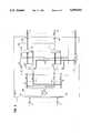
- FIG. 1is a block diagram of an illustrative telecommunication system embodying the invention
- FIG. 2is a block diagram of the communication format of the ring buses of the system of FIG. 1;
- FIG. 3is a block diagram of the switch of FIG. 1;
- FIG. 4is a block diagram of a time slot interchanger of the switch of FIG. 3.
- FIG. 1shows an illustrative communication system 10, which is illustratively a braodband integrated services digital network (BISDN).
- System 10comprises a plurality of ring networks 15 interconnected by a switch 11. Ring networks are well known in the art.
- a ring network 15comprises a ring bus 12 that functions as the communication medium of the network 15.
- bus 12is a serial, time-division, fiber optic bus operating at 45 Mbps.
- Connected to bus 12are a plurality of add/drop multiplexers ( ⁇ mux) 13, each one of which interfaces one or more units of terminal equipment (T.E.) 14 to bus 12.
- a multiplexer 13receives communications destined for its connected terminal equipment 14 over bus 12 and forwards them to connected terminal equipment 14.
- Multiplexer 13also receives communications from its connected terminal equipment 14 and transmits them over bus 12. Such multiplexers 13 are known in the art. Units of terminal equipment 14 are, for example, telephones, computers, audio transmiters and receivers, and video transmitters and receivers. Units of terminal equipment 14 may also include gateways to other communication systems.
- Network manager 16In one of the ring networks 15, and add/drop multiplexer 13 interfaces a network manager 16 to ring bus 12.
- Network manager 16is an intelligent unit (e.g., a computer) that controls the flow of communications within system 10. Specifically, manager 16 assigns bandwidth on buses 12 for use by multiplexers 13, and specifies the interconnections that are to be established and torn down by switch 11. For this latter purpose, manager 16 is communicatively connected to switch 11 by a control link 17. Communication network managers are well known in the art.
- FIG. 2shows the communication format used on bus 12.
- But 12is a synchronous communications medium. It carries communications in the form of repeating frames 200 each one of which comprises a plurality of time slots 201.
- Each frame 200illustratively consist of 5592 time slots 201, and each time slot 201 carries one bit data; consequently, both bits and time slots will subsequently be referred to by the numeral 201.
- Each frame 200has a duration of 125 ⁇ s, giving each time slot 201 and 8 Kbps bandwidth.
- Each time slot 201 of a frame 200may form a separate communications channel, or a plurality of time slots 201 of a frame 200 may be combined to form a higher-speed channel. In this example, the maximum channel bandwidth is 45 Mbps.
- Bandwidthmay be allocated to channels in one time slot 201, or 8 Kbps, increments. As shown in FIG. 2, some number of bits 201 of each frame 200 are used as framing and control bits 204. The number and placement of these bits 204 within a frame 200 are a function of the particular communication format adopted for buses 12. All but of the remaining time slots 201 of each frame 200 may be used to form customer channels 202, while the remaining one time slot 201 of each frame 200 is always reserved for a control channel 203. However, additional time slots 201 may be dynamically allocated to control channel 203, or to the information of additonal control channels 203, by network manager 16. Customer channels 202 are circuit-switched, while the one or more control channels 203 are message-based, e.g., packetized.
- Add/drop multiplexers 13communicate with network manager 16 via the one more control channels 203 in a conventional manner. Multiplexers 13 use channels 203 to request allocation and deallocation of time slots 201 to customer channels 202 for use by their connected terminal equipment 14, and to provide manager 16 with destination addresses for those channels 202. Multiplexers also use channels 203 to receive from manager 16 the requested allocations and deallocations, including information identifying the particular allocated and deallocated time slots 201, as well as information idetifying channels 202 incoming from terminal equipment 14 connected to other multiplexers 13. Multiplexers 13 retrieve information destined for their connected terminal equipment 14 from time slots 201 of the allocated incoming channels 202, and insert information from their connected equipment 14 into time slots 201 of the allocated outgoing channels 202.
- Switch 11is shown in FIG. 3.
- Switch 11includes a plurality of input ports 305 and a plurality of output ports 306. While in the example of FIG. 1, the number of input ports 305 and output ports 306 is the same, it need not always be so; the number of input ports may be greater than or smaller than the number of output ports.
- Each ring bus 12is connected to one input port 305 and one output port 306 of switch 11. Communication signals flow in a bus 12 in one direction only, and each bus 12 is connected to switch 11 in such a manner that communications flow from bus 12 into switch 11 at an input port 305 and flow from switch 11 into bus 12 at an output port 306. From input ports 305, incoming communications flow into a frame aligner circuit 300.
- Circuit 300ensures that transitions between two adjacent frames 200 incoming into switch 11 from a bus 12 occur at the same instant on all buses 12, in a conventional manner. Circuit 300 then outputs the frame-aligned communications to the remainder of switch 11 via links 120. A different link 120 serves each input port 305.
- Switch 11includes two stages of switching: a time stage 301 followed by a space stage 302.
- Time stage 301comprises a plurality of time slot interchangers (TSIs) 303, one for each output port 306. All links 120 are connected to inputs of each TSI 303. Consequently, each TSI 303 receives all communications incoming to switch 11 at every port 305, i.e., across every bus 12.
- Space stage 302is a time-multiplexed space switch that comprises a plurality of multiplexers 304, one for each TSI 303. The input of a different multiplexer 304 is connected to the output of each TSI 303, and the output of a different multiplexer 304 is connected to each bus 12 via an output port 306. Control over the operation of switch 11 is exercised by a controller 307. Controller 307 receives its instructions from network manager 16 via control link 17, and exercises its control over switch 11 via a control bus 310 that connects to each TSI 303.
- TSIstime
- TSI 303includes a data store 400 that stores a plurality of memory words 401.
- the number of words 401is twice the number of time slots 201 in a frame 200, or 11184 words.
- Each word 401has a plurality of bits 405, one bit 405 for each input port 305.
- Each bit 405 position in words 401has a bit-serial input connected to a different link 120.
- Each bit 405 position in words 401also has a bit-serial output, giving data store 400 a word 401-wide bit-parallel output which is connected to a bit-parallel input of multiplexer 304.
- Counter 402is a cyclical counter that sequentially generates the numbers of twice the number of time slots 201 of a frame 200 once every two frame time periods. These numbers are applied as addresses of sequential words 401 to a write address control input of data store 400, where they control the storage of data coming into data store 400 on each link 120.
- each word 401is write-addressed once every two frame 200 time periods; each word 401 stores one bit 201 from each bus 12; successive words 401 store successive incoming bits 201; and words 401 together store up to two successive frames 200 from each bus 12.
- Control store 403stores a plurality of memory words 404, one for each time slot 201 of two frames 200. Each control store 403 word 404 contains the address (i.e., the number) of a data store 400 word 401 and of a bit 405 within that word 401.
- the contents of the control store 403 word 404 which is addressed therbyare output by control store 403.
- the portion thereof that identifies a word 401is applied to a read address control input of data store 400, and a portion that identifies a bit 405 within that word 401 is applied to a select control input of multiplexer 304.
- the address control input of data store 400determines which word 401 is supplied by data store 400 to multiplexer 304, and the select control input of multiplexer 304 to the connected output port 306. As a result, during each time slot 201 period, a word is read out from data store 400 and a bit of that word 401 is output by a multiplexer 304 onto the connected bus 12.
- the read and write addresses supplied to data store 400always address words 401 in different halves of data store 400, i.e., while bits 201 of a frame 200 that is stored in data store 400 are being read out, bits 201 of the successive incoming frame 200 are being written into data store 400. This occurs at each TSI 303 and multiplexer 304.
- R maxthe highest per-channel bit rate that is to be handled
- R minthe lowest per-channel (including substrate channel) bit rate that is to be handled
- a time slot 201 from every link 120is received by data store 400 of each time slot interchanger 303 every time slot period. Simultaneously-received time slots 201, one from each link 120 are stored in a single word 401 of data store 400; successively-received time slots 201 are stored in successive words 401. Consequently, every time slot interchanger 303 receives the same input.
- control store 403uses the READ ADDR line to read out of data store 400 the word 401 which stores the particular, selected time slot 201 of each of the received frames 200.
- control stores 403 of different time slot interchangers 303may select the same word 401 or different words 401 of their corresponding data stores 400. Also during each time slot period, the particular time slot 201 of a particular received frame 200 is selected by multiplexer 304: control store 403 uses the SEL control input of multiplexer 304 to select only one of the bits 405 of the word 401 that has been read out of data store 400. The selected time slot 201 of the selected frame 200 is then transmitted at output port 306. Again, during a time slot period, multiplexers 304 associated with different time slot interchangers 303 may select the same bit 405 or different bits 405 of a read-out word 401. Thus, during any time slot period, different output ports 306 may transmit the same time slot 201 of the same frame 200, or different time slots 201 of the same frame 200, or the same slot 201 of different frames 200, or different time slots 201 of different frames 200.
- any time slot 201 incoming to switch 11 on any bus 12can be switched by switch 11 to any outgoing time slot 201 of any bus 12, in a completely non-blocking manner, and with only a one frame 200 time delay caused by switch 11. Furthermore, any incoming time slot 201 can be switched to a plurality of outgoing time slots, giving switch 11 a broadcasting capability without increasing the time delay caused by switch 11.
- Control store 403is programmed by controller 307 via control bus 310. Controller 307 applies addresses of words 404 to a write address control input of control store 403 at the same time that it applies data that is to be stored by words 404 to a data input of control store 403.
Landscapes
- Engineering & Computer Science (AREA)
- Computer Networks & Wireless Communication (AREA)
- Signal Processing (AREA)
- Data Exchanges In Wide-Area Networks (AREA)
Abstract
Description
Claims (17)
Priority Applications (1)
| Application Number | Priority Date | Filing Date | Title |
|---|---|---|---|
| US07/441,794US4999832A (en) | 1989-11-27 | 1989-11-27 | Broadband multirate switching architecture |
Applications Claiming Priority (1)
| Application Number | Priority Date | Filing Date | Title |
|---|---|---|---|
| US07/441,794US4999832A (en) | 1989-11-27 | 1989-11-27 | Broadband multirate switching architecture |
Publications (1)
| Publication Number | Publication Date |
|---|---|
| US4999832Atrue US4999832A (en) | 1991-03-12 |
Family
ID=23754314
Family Applications (1)
| Application Number | Title | Priority Date | Filing Date |
|---|---|---|---|
| US07/441,794Expired - LifetimeUS4999832A (en) | 1989-11-27 | 1989-11-27 | Broadband multirate switching architecture |
Country Status (1)
| Country | Link |
|---|---|
| US (1) | US4999832A (en) |
Cited By (36)
| Publication number | Priority date | Publication date | Assignee | Title |
|---|---|---|---|---|
| US5208806A (en)* | 1989-11-17 | 1993-05-04 | Fujitsu Limited | Isdn terminal equipment operating with circuit switching mode and packet switching mode |
| WO1993012625A1 (en)* | 1991-12-16 | 1993-06-24 | Telefonaktiebolaget Lm Ericsson | A uniswitch comprising a plurality of units which are distributed locally and which are connected by means of physical links |
| EP0529649A3 (en)* | 1991-08-30 | 1993-08-18 | Nec Corporation | Virtual tributary path idle insertion using timeslot interchange |
| US5249184A (en)* | 1990-01-30 | 1993-09-28 | Johnson Service Company | Network control system with improved reliability |
| US5282199A (en)* | 1992-12-29 | 1994-01-25 | International Business Machines Corporation | Method and apparatus for interoperation of FDDI-I and FDDI-II networks |
| US5299312A (en)* | 1990-11-15 | 1994-03-29 | Massachusetts Institute Of Technology | Network fault recovery by controllable switching of subnetworks |
| US5329524A (en)* | 1992-10-20 | 1994-07-12 | At&T Bell Laboratories | TDM circuit-switching arrangement that handles frames of different sizes |
| US5412650A (en)* | 1992-09-05 | 1995-05-02 | U.S. Philips Corporation | Method of, and system for, transmitting data over a communications channel |
| EP0663743A1 (en)* | 1993-12-27 | 1995-07-19 | Mitsubishi Denki Kabushiki Kaisha | Time-division multiplexer with reduced delay time |
| US5453985A (en)* | 1992-02-10 | 1995-09-26 | Telefonaktiebolaget Lm Ericsson | Digital bit oriented switch, general digital switch and PCM transmission system |
| WO1995028779A1 (en)* | 1994-04-15 | 1995-10-26 | Dsc Communications Corporation | Multi-service switch for a telecommunications network |
| US5469428A (en)* | 1991-03-26 | 1995-11-21 | Nippon Telegraph And Telephone Corporation | Loop-back system in a dual ring network |
| US5742774A (en)* | 1995-11-03 | 1998-04-21 | Lucent Technologies Inc | Multi-ring SONET architecture having shared gateways daisy chained to complete the main and subsidiary ring controlled by a common master controller |
| WO1998020651A1 (en)* | 1996-11-06 | 1998-05-14 | Pluris, Inc. | Fault-tolerant butterfly switch |
| US5796795A (en)* | 1994-11-30 | 1998-08-18 | Gte Laboratories Incorporated | Data transferring circuit which aligns clock and data |
| WO1999022496A1 (en)* | 1997-10-28 | 1999-05-06 | Abrizio, Inc. | Stream-line data network |
| FR2779312A1 (en)* | 1998-03-20 | 1999-12-03 | Fujitsu Ltd | CIRCUIT ASSIGNING TIME WINDOWS |
| EP0964337A1 (en)* | 1998-06-12 | 1999-12-15 | ELA MEDICAL (Société anonyme) | Interconnection structure to exchange data between the various addressable devices of a microcomputer |
| EP0752768A3 (en)* | 1995-07-06 | 1999-12-22 | Telia Ab | Telecommunication system and network element at telecommunication system |
| US6058427A (en)* | 1997-02-14 | 2000-05-02 | Advanced Micro Devices, Inc. | Apparatus and method for generating a serial data stream carrying data for multiple network switch ports for use by a physical transceiver |
| US6128113A (en)* | 1998-03-04 | 2000-10-03 | Dynamics Research Corporation | Transparent optical communications switch |
| US6175552B1 (en)* | 1997-07-25 | 2001-01-16 | Nortel Networks Limited | Disaster recovery in a telecommunications network |
| US6490247B1 (en) | 1996-06-26 | 2002-12-03 | Gateway, Inc | Ring-ordered dynamically reconfigurable network using an existing communications system |
| US20030002541A1 (en)* | 2001-06-07 | 2003-01-02 | Fowler Michael L. | Mid-connect architecture with point-to-point connections for high speed data transfer |
| US6567429B1 (en) | 1998-06-02 | 2003-05-20 | Dynamics Research Corporation | Wide area multi-service broadband network |
| US20040023558A1 (en)* | 2001-06-07 | 2004-02-05 | Fowler Michael L. | Mid-connect architecture with point-to-point connections for high speed data transfer |
| US6747985B1 (en)* | 1998-08-03 | 2004-06-08 | Samsung Electronics Co., Ltd. | Systems and methods for optimizing communications in an ethernet network |
| US6748451B2 (en) | 1998-05-26 | 2004-06-08 | Dow Global Technologies Inc. | Distributed computing environment using real-time scheduling logic and time deterministic architecture |
| US6895015B1 (en)* | 1999-05-05 | 2005-05-17 | Advanced Micro Devices, Inc. | Dynamic time slot allocation in internal rules checker scheduler |
| EP0944279A3 (en)* | 1998-03-20 | 2005-06-22 | Fujitsu Limited | Time slot assignment circuit |
| US6970455B2 (en)* | 1998-11-13 | 2005-11-29 | Lucent Technologies Inc. | Space/time switch architecture |
| EP1633065A3 (en)* | 1996-11-21 | 2008-05-14 | Yazaki Corporation | Transmitter, receiver, communication apparatus, communication method and communication system |
| US20080304508A1 (en)* | 2007-06-07 | 2008-12-11 | Fujitsu Limited | Time slot interchanger |
| US20120213229A1 (en)* | 2011-02-17 | 2012-08-23 | Bradley Ronald Kangas | Method and Apparatus for an Expandable Switching Element |
| JP2015041946A (en)* | 2013-08-23 | 2015-03-02 | 日本電信電話株式会社 | Node |
| JP2015133646A (en)* | 2014-01-15 | 2015-07-23 | 日本電信電話株式会社 | Node and scheduler |
Citations (17)
| Publication number | Priority date | Publication date | Assignee | Title |
|---|---|---|---|---|
| US3890471A (en)* | 1973-12-17 | 1975-06-17 | Bell Telephone Labor Inc | Loop data transmission arrangement employing an interloop communication terminal |
| US4206322A (en)* | 1978-09-25 | 1980-06-03 | Bell Telephone Laboratories, Incorporated | Time-division switching system for multirate data |
| US4322843A (en)* | 1979-12-26 | 1982-03-30 | Bell Telephone Laboratories, Incorporated | Control information communication arrangement for a time division switching system |
| US4485469A (en)* | 1982-08-30 | 1984-11-27 | At&T Bell Laboratories | Time slot interchanger |
| US4547877A (en)* | 1983-06-09 | 1985-10-15 | At&T Bell Laboratories | System for switching multirate digitized voice and data |
| US4553234A (en)* | 1983-01-06 | 1985-11-12 | U.S. Philips Corporation | Method and system of transmitting digital information in a transmission ring |
| US4558444A (en)* | 1983-05-11 | 1985-12-10 | At&T Laboratories | Switching system having selectively interconnected remote switching modules |
| US4587651A (en)* | 1983-05-04 | 1986-05-06 | Cxc Corporation | Distributed variable bandwidth switch for voice, data, and image communications |
| US4630259A (en)* | 1984-11-14 | 1986-12-16 | At&T Bell Laboratories | Lockup detection and recovery in a packet switching network |
| US4679191A (en)* | 1983-05-04 | 1987-07-07 | Cxc Corporation | Variable bandwidth switching system |
| US4713807A (en)* | 1985-05-24 | 1987-12-15 | Stc Plc | Intelligence transmission system of the local area network type |
| US4718058A (en)* | 1984-02-24 | 1988-01-05 | Staat Der Nederlanden | Digital switching network for switching signals of different bit rates |
| US4736371A (en)* | 1985-12-30 | 1988-04-05 | Nec Corporation | Satellite communications system with random multiple access and time slot reservation |
| US4763317A (en)* | 1985-12-13 | 1988-08-09 | American Telephone And Telegraph Company, At&T Bell Laboratories | Digital communication network architecture for providing universal information services |
| US4769839A (en)* | 1983-05-31 | 1988-09-06 | Ostereichisehes Forschungszentrum Seibersdorf G.m.b.H. | Method and device for the transfer of data in a data loop |
| US4780870A (en)* | 1986-09-05 | 1988-10-25 | American Telephone And Telegraph Company, At&T Bell Laboratories | Packet switch |
| US4821259A (en)* | 1986-09-05 | 1989-04-11 | American Telephone And Telegraph Company, At&T Bell Laboratories | Control information communication arrangement for a distributed control switching system |
- 1989
- 1989-11-27USUS07/441,794patent/US4999832A/ennot_activeExpired - Lifetime
Patent Citations (17)
| Publication number | Priority date | Publication date | Assignee | Title |
|---|---|---|---|---|
| US3890471A (en)* | 1973-12-17 | 1975-06-17 | Bell Telephone Labor Inc | Loop data transmission arrangement employing an interloop communication terminal |
| US4206322A (en)* | 1978-09-25 | 1980-06-03 | Bell Telephone Laboratories, Incorporated | Time-division switching system for multirate data |
| US4322843A (en)* | 1979-12-26 | 1982-03-30 | Bell Telephone Laboratories, Incorporated | Control information communication arrangement for a time division switching system |
| US4485469A (en)* | 1982-08-30 | 1984-11-27 | At&T Bell Laboratories | Time slot interchanger |
| US4553234A (en)* | 1983-01-06 | 1985-11-12 | U.S. Philips Corporation | Method and system of transmitting digital information in a transmission ring |
| US4587651A (en)* | 1983-05-04 | 1986-05-06 | Cxc Corporation | Distributed variable bandwidth switch for voice, data, and image communications |
| US4679191A (en)* | 1983-05-04 | 1987-07-07 | Cxc Corporation | Variable bandwidth switching system |
| US4558444A (en)* | 1983-05-11 | 1985-12-10 | At&T Laboratories | Switching system having selectively interconnected remote switching modules |
| US4769839A (en)* | 1983-05-31 | 1988-09-06 | Ostereichisehes Forschungszentrum Seibersdorf G.m.b.H. | Method and device for the transfer of data in a data loop |
| US4547877A (en)* | 1983-06-09 | 1985-10-15 | At&T Bell Laboratories | System for switching multirate digitized voice and data |
| US4718058A (en)* | 1984-02-24 | 1988-01-05 | Staat Der Nederlanden | Digital switching network for switching signals of different bit rates |
| US4630259A (en)* | 1984-11-14 | 1986-12-16 | At&T Bell Laboratories | Lockup detection and recovery in a packet switching network |
| US4713807A (en)* | 1985-05-24 | 1987-12-15 | Stc Plc | Intelligence transmission system of the local area network type |
| US4763317A (en)* | 1985-12-13 | 1988-08-09 | American Telephone And Telegraph Company, At&T Bell Laboratories | Digital communication network architecture for providing universal information services |
| US4736371A (en)* | 1985-12-30 | 1988-04-05 | Nec Corporation | Satellite communications system with random multiple access and time slot reservation |
| US4780870A (en)* | 1986-09-05 | 1988-10-25 | American Telephone And Telegraph Company, At&T Bell Laboratories | Packet switch |
| US4821259A (en)* | 1986-09-05 | 1989-04-11 | American Telephone And Telegraph Company, At&T Bell Laboratories | Control information communication arrangement for a distributed control switching system |
Non-Patent Citations (2)
| Title |
|---|
| D. L. Carney et al., "The 5ESS Switching System: Architectural Overview", AT&T Technical Journal, vol. 64, No. 6 (Jul.-Aug. 85), pp. 1339-1357. |
| D. L. Carney et al., The 5ESS Switching System: Architectural Overview , AT&T Technical Journal, vol. 64, No. 6 (Jul. Aug. 85), pp. 1339 1357.* |
Cited By (48)
| Publication number | Priority date | Publication date | Assignee | Title |
|---|---|---|---|---|
| US5208806A (en)* | 1989-11-17 | 1993-05-04 | Fujitsu Limited | Isdn terminal equipment operating with circuit switching mode and packet switching mode |
| US5249184A (en)* | 1990-01-30 | 1993-09-28 | Johnson Service Company | Network control system with improved reliability |
| US5299312A (en)* | 1990-11-15 | 1994-03-29 | Massachusetts Institute Of Technology | Network fault recovery by controllable switching of subnetworks |
| US5469428A (en)* | 1991-03-26 | 1995-11-21 | Nippon Telegraph And Telephone Corporation | Loop-back system in a dual ring network |
| US5434858A (en)* | 1991-08-30 | 1995-07-18 | Nec Corporation | Virtual tributary path idle insertion using timeslot interchange |
| EP0529649A3 (en)* | 1991-08-30 | 1993-08-18 | Nec Corporation | Virtual tributary path idle insertion using timeslot interchange |
| AU667863B2 (en)* | 1991-12-16 | 1996-04-18 | Telefonaktiebolaget Lm Ericsson (Publ) | A uniswitch comprising a plurality of units which are distributed locally and which are connected by means of physical links |
| US5347513A (en)* | 1991-12-16 | 1994-09-13 | Telefonaktiebolaget L M Ericsson | Fast operating program controlled digital uniswitch |
| WO1993012625A1 (en)* | 1991-12-16 | 1993-06-24 | Telefonaktiebolaget Lm Ericsson | A uniswitch comprising a plurality of units which are distributed locally and which are connected by means of physical links |
| US5453985A (en)* | 1992-02-10 | 1995-09-26 | Telefonaktiebolaget Lm Ericsson | Digital bit oriented switch, general digital switch and PCM transmission system |
| US5412650A (en)* | 1992-09-05 | 1995-05-02 | U.S. Philips Corporation | Method of, and system for, transmitting data over a communications channel |
| US5329524A (en)* | 1992-10-20 | 1994-07-12 | At&T Bell Laboratories | TDM circuit-switching arrangement that handles frames of different sizes |
| US5282199A (en)* | 1992-12-29 | 1994-01-25 | International Business Machines Corporation | Method and apparatus for interoperation of FDDI-I and FDDI-II networks |
| EP0663743A1 (en)* | 1993-12-27 | 1995-07-19 | Mitsubishi Denki Kabushiki Kaisha | Time-division multiplexer with reduced delay time |
| US5521920A (en)* | 1993-12-27 | 1996-05-28 | Mitsubishi Denki Kabushiki Kaisha | Time-division multiplexer with reduced delay time |
| WO1995028779A1 (en)* | 1994-04-15 | 1995-10-26 | Dsc Communications Corporation | Multi-service switch for a telecommunications network |
| US5526349A (en)* | 1994-04-15 | 1996-06-11 | Dsc Communications Corporation | Data formats for telecommunications networks |
| US5796795A (en)* | 1994-11-30 | 1998-08-18 | Gte Laboratories Incorporated | Data transferring circuit which aligns clock and data |
| EP0752768A3 (en)* | 1995-07-06 | 1999-12-22 | Telia Ab | Telecommunication system and network element at telecommunication system |
| US5742774A (en)* | 1995-11-03 | 1998-04-21 | Lucent Technologies Inc | Multi-ring SONET architecture having shared gateways daisy chained to complete the main and subsidiary ring controlled by a common master controller |
| US6490247B1 (en) | 1996-06-26 | 2002-12-03 | Gateway, Inc | Ring-ordered dynamically reconfigurable network using an existing communications system |
| WO1998020651A1 (en)* | 1996-11-06 | 1998-05-14 | Pluris, Inc. | Fault-tolerant butterfly switch |
| US5940367A (en)* | 1996-11-06 | 1999-08-17 | Pluris, Inc. | Fault-tolerant butterfly switch |
| EP1633065A3 (en)* | 1996-11-21 | 2008-05-14 | Yazaki Corporation | Transmitter, receiver, communication apparatus, communication method and communication system |
| US6058427A (en)* | 1997-02-14 | 2000-05-02 | Advanced Micro Devices, Inc. | Apparatus and method for generating a serial data stream carrying data for multiple network switch ports for use by a physical transceiver |
| US6175552B1 (en)* | 1997-07-25 | 2001-01-16 | Nortel Networks Limited | Disaster recovery in a telecommunications network |
| WO1999022496A1 (en)* | 1997-10-28 | 1999-05-06 | Abrizio, Inc. | Stream-line data network |
| US6128113A (en)* | 1998-03-04 | 2000-10-03 | Dynamics Research Corporation | Transparent optical communications switch |
| EP0944279A3 (en)* | 1998-03-20 | 2005-06-22 | Fujitsu Limited | Time slot assignment circuit |
| FR2779312A1 (en)* | 1998-03-20 | 1999-12-03 | Fujitsu Ltd | CIRCUIT ASSIGNING TIME WINDOWS |
| US6587459B1 (en)* | 1998-03-20 | 2003-07-01 | Fujitsu Limited | Time slot assignment circuit |
| US6748451B2 (en) | 1998-05-26 | 2004-06-08 | Dow Global Technologies Inc. | Distributed computing environment using real-time scheduling logic and time deterministic architecture |
| US6567429B1 (en) | 1998-06-02 | 2003-05-20 | Dynamics Research Corporation | Wide area multi-service broadband network |
| US6532238B1 (en) | 1998-06-12 | 2003-03-11 | Ela Medical S.A. | Interconnection between addressable elements of a microcomputer for active implantable medical devices |
| EP0964337A1 (en)* | 1998-06-12 | 1999-12-15 | ELA MEDICAL (Société anonyme) | Interconnection structure to exchange data between the various addressable devices of a microcomputer |
| FR2779844A1 (en)* | 1998-06-12 | 1999-12-17 | Ela Medical Sa | INTERCONNECTION STRUCTURE BETWEEN ADDRESSABLE ORGANS OF A MICROCALCULATOR, IN PARTICULAR FOR AN IMPLANTABLE ACTIVE MEDICAL DEVICE SUCH AS A CARDIAC STIMULATOR OR DEFIBRILLATOR |
| US6747985B1 (en)* | 1998-08-03 | 2004-06-08 | Samsung Electronics Co., Ltd. | Systems and methods for optimizing communications in an ethernet network |
| US6970455B2 (en)* | 1998-11-13 | 2005-11-29 | Lucent Technologies Inc. | Space/time switch architecture |
| US6895015B1 (en)* | 1999-05-05 | 2005-05-17 | Advanced Micro Devices, Inc. | Dynamic time slot allocation in internal rules checker scheduler |
| US20030002541A1 (en)* | 2001-06-07 | 2003-01-02 | Fowler Michael L. | Mid-connect architecture with point-to-point connections for high speed data transfer |
| US20040023558A1 (en)* | 2001-06-07 | 2004-02-05 | Fowler Michael L. | Mid-connect architecture with point-to-point connections for high speed data transfer |
| US20080304508A1 (en)* | 2007-06-07 | 2008-12-11 | Fujitsu Limited | Time slot interchanger |
| CN101321403B (en)* | 2007-06-07 | 2012-03-07 | 富士通株式会社 | Time slot interchanger |
| US8582597B2 (en) | 2007-06-07 | 2013-11-12 | Fujitsu Limited | Time slot interchanger |
| US20120213229A1 (en)* | 2011-02-17 | 2012-08-23 | Bradley Ronald Kangas | Method and Apparatus for an Expandable Switching Element |
| US9215192B2 (en)* | 2011-02-17 | 2015-12-15 | Tellabs Operations, Inc. | Method and apparatus for an expandable switching element |
| JP2015041946A (en)* | 2013-08-23 | 2015-03-02 | 日本電信電話株式会社 | Node |
| JP2015133646A (en)* | 2014-01-15 | 2015-07-23 | 日本電信電話株式会社 | Node and scheduler |
Similar Documents
| Publication | Publication Date | Title |
|---|---|---|
| US4999832A (en) | Broadband multirate switching architecture | |
| US5533018A (en) | Multi-protocol packet framing over an isochronous network | |
| JP2890348B2 (en) | Telephone subscriber accommodation in broadband networks. | |
| US4763319A (en) | Multi-rate synchronous virtual circuit network for voice and data communications | |
| US5519700A (en) | Telecommunication system with synchronous-asynchronous interface | |
| US4893306A (en) | Method and apparatus for multiplexing circuit and packet traffic | |
| US5115427A (en) | Arrangements for switching multiple packet types combined in a single packet stream | |
| EP0450818B1 (en) | Broadband ISDN packet switching arrangements | |
| US4855999A (en) | DTDM multiplexer with cross-point switch | |
| US4704716A (en) | Method and apparatus for establishing a wideband communication facility through a communication network having narrow bandwidth channels | |
| US4833673A (en) | Time division multiplexer for DTDM bit streams | |
| US4866703A (en) | Integrated services digital network module | |
| JP2761872B2 (en) | Multiple information exchange method and apparatus therefor | |
| EP0266530B1 (en) | A method of controlling a multi-stage interconnection network | |
| US4819226A (en) | Framer circuit for use in a DTDM network | |
| US5696761A (en) | Method and apparatus for interfacing low speed access links to a high speed time multiplexed switch fabric | |
| US5467346A (en) | Packet communication method and packet communication apparatus | |
| RU2134024C1 (en) | Device and method of processing of elements of data on mode of asynchronous transmission in system of commutation of mode of asynchronous transmission | |
| JPH03173243A (en) | Network node interface of digital communication system | |
| US4811332A (en) | Apparatus and method for TDM data switching | |
| US5787087A (en) | Method and apparatus for interconnecting a plurality of terminal equipments to the ISDN | |
| US6430186B1 (en) | Asynchronous bit-table calendar for ATM switch | |
| JPH089058A (en) | Multiplexer with transmission line backup function | |
| CA2002999A1 (en) | Packet-switching exchange and input converter unit therefor | |
| JPH11331267A (en) | Subscriber line transmitter |
Legal Events
| Date | Code | Title | Description |
|---|---|---|---|
| AS | Assignment | Owner name:AT&T INFORMATION SYSTEMS INC., 100 SOUTHGATE PARKW Free format text:ASSIGNMENT OF ASSIGNORS INTEREST.;ASSIGNORS:CHEN, HUNG-SAN;FARLEIGH, SCOTT E.;HELTON, JOHN S.;AND OTHERS;REEL/FRAME:005188/0949;SIGNING DATES FROM 19891122 TO 19891127 Owner name:AMERICAN TELEPHONE AND TELEGRAPH COMPANY, 550 MADI Free format text:ASSIGNMENT OF ASSIGNORS INTEREST.;ASSIGNORS:CHEN, HUNG-SAN;FARLEIGH, SCOTT E.;HELTON, JOHN S.;AND OTHERS;REEL/FRAME:005188/0949;SIGNING DATES FROM 19891122 TO 19891127 | |
| STCF | Information on status: patent grant | Free format text:PATENTED CASE | |
| FPAY | Fee payment | Year of fee payment:4 | |
| FEPP | Fee payment procedure | Free format text:PAYER NUMBER DE-ASSIGNED (ORIGINAL EVENT CODE: RMPN); ENTITY STATUS OF PATENT OWNER: LARGE ENTITY Free format text:PAYOR NUMBER ASSIGNED (ORIGINAL EVENT CODE: ASPN); ENTITY STATUS OF PATENT OWNER: LARGE ENTITY | |
| FEPP | Fee payment procedure | Free format text:PAYOR NUMBER ASSIGNED (ORIGINAL EVENT CODE: ASPN); ENTITY STATUS OF PATENT OWNER: LARGE ENTITY | |
| FPAY | Fee payment | Year of fee payment:8 | |
| AS | Assignment | Owner name:LUCENT TECHNOLOGIES, INC., NEW JERSEY Free format text:ASSIGNMENT OF ASSIGNORS INTEREST;ASSIGNOR:AT&T CORP.;REEL/FRAME:012754/0365 Effective date:19960329 Owner name:AVAYA TECHNOLOGY CORP., NEW JERSEY Free format text:ASSIGNMENT OF ASSIGNORS INTEREST;ASSIGNOR:LUCENT TECHNOLOGIES INC.;REEL/FRAME:012754/0770 Effective date:20000929 | |
| AS | Assignment | Owner name:BANK OF NEW YORK, THE, NEW YORK Free format text:SECURITY INTEREST;ASSIGNOR:AVAYA TECHNOLOGY CORP.;REEL/FRAME:012762/0160 Effective date:20020405 | |
| FPAY | Fee payment | Year of fee payment:12 | |
| AS | Assignment | Owner name:CITIBANK, N.A., AS ADMINISTRATIVE AGENT, NEW YORK Free format text:SECURITY AGREEMENT;ASSIGNORS:AVAYA, INC.;AVAYA TECHNOLOGY LLC;OCTEL COMMUNICATIONS LLC;AND OTHERS;REEL/FRAME:020156/0149 Effective date:20071026 Owner name:CITIBANK, N.A., AS ADMINISTRATIVE AGENT,NEW YORK Free format text:SECURITY AGREEMENT;ASSIGNORS:AVAYA, INC.;AVAYA TECHNOLOGY LLC;OCTEL COMMUNICATIONS LLC;AND OTHERS;REEL/FRAME:020156/0149 Effective date:20071026 | |
| AS | Assignment | Owner name:CITICORP USA, INC., AS ADMINISTRATIVE AGENT, NEW Y Free format text:SECURITY AGREEMENT;ASSIGNORS:AVAYA, INC.;AVAYA TECHNOLOGY LLC;OCTEL COMMUNICATIONS LLC;AND OTHERS;REEL/FRAME:020166/0705 Effective date:20071026 Owner name:CITICORP USA, INC., AS ADMINISTRATIVE AGENT, NEW YORK Free format text:SECURITY AGREEMENT;ASSIGNORS:AVAYA, INC.;AVAYA TECHNOLOGY LLC;OCTEL COMMUNICATIONS LLC;AND OTHERS;REEL/FRAME:020166/0705 Effective date:20071026 Owner name:CITICORP USA, INC., AS ADMINISTRATIVE AGENT,NEW YO Free format text:SECURITY AGREEMENT;ASSIGNORS:AVAYA, INC.;AVAYA TECHNOLOGY LLC;OCTEL COMMUNICATIONS LLC;AND OTHERS;REEL/FRAME:020166/0705 Effective date:20071026 | |
| AS | Assignment | Owner name:AVAYA INC., NEW JERSEY Free format text:REASSIGNMENT;ASSIGNOR:AVAYA TECHNOLOGY LLC;REEL/FRAME:021158/0290 Effective date:20080625 | |
| FEPP | Fee payment procedure | Free format text:PAYER NUMBER DE-ASSIGNED (ORIGINAL EVENT CODE: RMPN); ENTITY STATUS OF PATENT OWNER: LARGE ENTITY Free format text:PAYOR NUMBER ASSIGNED (ORIGINAL EVENT CODE: ASPN); ENTITY STATUS OF PATENT OWNER: LARGE ENTITY | |
| AS | Assignment | Owner name:AVAYA TECHNOLOGY LLC, NEW JERSEY Free format text:CONVERSION FROM CORP TO LLC;ASSIGNOR:AVAYA TECHNOLOGY CORP.;REEL/FRAME:022071/0420 Effective date:20051004 | |
| AS | Assignment | Owner name:OCTEL COMMUNICATIONS LLC, CALIFORNIA Free format text:RELEASE BY SECURED PARTY;ASSIGNOR:CITICORP USA, INC.;REEL/FRAME:045032/0213 Effective date:20171215 Owner name:SIERRA HOLDINGS CORP., NEW JERSEY Free format text:RELEASE BY SECURED PARTY;ASSIGNOR:CITICORP USA, INC.;REEL/FRAME:045032/0213 Effective date:20171215 Owner name:AVAYA, INC., CALIFORNIA Free format text:RELEASE BY SECURED PARTY;ASSIGNOR:CITICORP USA, INC.;REEL/FRAME:045032/0213 Effective date:20171215 Owner name:VPNET TECHNOLOGIES, INC., NEW JERSEY Free format text:RELEASE BY SECURED PARTY;ASSIGNOR:CITICORP USA, INC.;REEL/FRAME:045032/0213 Effective date:20171215 Owner name:AVAYA TECHNOLOGY, LLC, NEW JERSEY Free format text:RELEASE BY SECURED PARTY;ASSIGNOR:CITICORP USA, INC.;REEL/FRAME:045032/0213 Effective date:20171215 |