US4999812A - Architecture for a flash erase EEPROM memory - Google Patents
Architecture for a flash erase EEPROM memoryDownload PDFInfo
- Publication number
- US4999812A US4999812AUS07/275,380US27538088AUS4999812AUS 4999812 AUS4999812 AUS 4999812AUS 27538088 AUS27538088 AUS 27538088AUS 4999812 AUS4999812 AUS 4999812A
- Authority
- US
- United States
- Prior art keywords
- region
- drain
- source
- programming
- gate electrode
- Prior art date
- Legal status (The legal status is an assumption and is not a legal conclusion. Google has not performed a legal analysis and makes no representation as to the accuracy of the status listed.)
- Expired - Fee Related
Links
- 230000015654memoryEffects0.000titleclaimsabstractdescription90
- 230000001965increasing effectEffects0.000claimsabstractdescription18
- 230000015556catabolic processEffects0.000claimsdescription15
- 239000002784hot electronSubstances0.000claimsdescription4
- 238000002955isolationMethods0.000claimsdescription4
- 238000007599dischargingMethods0.000claims3
- 238000002347injectionMethods0.000claims2
- 239000007924injectionSubstances0.000claims2
- 230000003071parasitic effectEffects0.000claims2
- 230000004044responseEffects0.000claims1
- 230000006870functionEffects0.000abstractdescription2
- 238000011017operating methodMethods0.000abstractdescription2
- 238000010586diagramMethods0.000description6
- 239000007943implantSubstances0.000description6
- 230000003247decreasing effectEffects0.000description3
- 229910021420polycrystalline siliconInorganic materials0.000description3
- 230000005689Fowler Nordheim tunnelingEffects0.000description2
- 230000007423decreaseEffects0.000description2
- 230000002939deleterious effectEffects0.000description2
- ZOXJGFHDIHLPTG-UHFFFAOYSA-NBoronChemical compound[B]ZOXJGFHDIHLPTG-UHFFFAOYSA-N0.000description1
- XUIMIQQOPSSXEZ-UHFFFAOYSA-NSiliconChemical group[Si]XUIMIQQOPSSXEZ-UHFFFAOYSA-N0.000description1
- 229910052796boronInorganic materials0.000description1
- 239000000872bufferSubstances0.000description1
- 230000001186cumulative effectEffects0.000description1
- 230000001419dependent effectEffects0.000description1
- 238000009792diffusion processMethods0.000description1
- 230000005684electric fieldEffects0.000description1
- 230000002708enhancing effectEffects0.000description1
- 230000036039immunityEffects0.000description1
- 238000001465metallisationMethods0.000description1
- 238000012986modificationMethods0.000description1
- 230000004048modificationEffects0.000description1
- 230000002093peripheral effectEffects0.000description1
- 230000005641tunnelingEffects0.000description1
Images


Classifications
- G—PHYSICS
- G11—INFORMATION STORAGE
- G11C—STATIC STORES
- G11C17/00—Read-only memories programmable only once; Semi-permanent stores, e.g. manually-replaceable information cards
- G—PHYSICS
- G11—INFORMATION STORAGE
- G11C—STATIC STORES
- G11C16/00—Erasable programmable read-only memories
- G11C16/02—Erasable programmable read-only memories electrically programmable
- G11C16/06—Auxiliary circuits, e.g. for writing into memory
- G11C16/34—Determination of programming status, e.g. threshold voltage, overprogramming or underprogramming, retention
- G11C16/3418—Disturbance prevention or evaluation; Refreshing of disturbed memory data
- G11C16/3427—Circuits or methods to prevent or reduce disturbance of the state of a memory cell when neighbouring cells are read or written
- G—PHYSICS
- G11—INFORMATION STORAGE
- G11C—STATIC STORES
- G11C16/00—Erasable programmable read-only memories
- G11C16/02—Erasable programmable read-only memories electrically programmable
- G11C16/06—Auxiliary circuits, e.g. for writing into memory
- G11C16/26—Sensing or reading circuits; Data output circuits
- G—PHYSICS
- G11—INFORMATION STORAGE
- G11C—STATIC STORES
- G11C16/00—Erasable programmable read-only memories
- G11C16/02—Erasable programmable read-only memories electrically programmable
- G11C16/06—Auxiliary circuits, e.g. for writing into memory
- G11C16/34—Determination of programming status, e.g. threshold voltage, overprogramming or underprogramming, retention
- G11C16/3418—Disturbance prevention or evaluation; Refreshing of disturbed memory data
- H—ELECTRICITY
- H10—SEMICONDUCTOR DEVICES; ELECTRIC SOLID-STATE DEVICES NOT OTHERWISE PROVIDED FOR
- H10D—INORGANIC ELECTRIC SEMICONDUCTOR DEVICES
- H10D30/00—Field-effect transistors [FET]
- H10D30/60—Insulated-gate field-effect transistors [IGFET]
- H10D30/68—Floating-gate IGFETs
- H10D30/681—Floating-gate IGFETs having only two programming levels
- H10D30/683—Floating-gate IGFETs having only two programming levels programmed by tunnelling of carriers, e.g. Fowler-Nordheim tunnelling
- H—ELECTRICITY
- H10—SEMICONDUCTOR DEVICES; ELECTRIC SOLID-STATE DEVICES NOT OTHERWISE PROVIDED FOR
- H10D—INORGANIC ELECTRIC SEMICONDUCTOR DEVICES
- H10D30/00—Field-effect transistors [FET]
- H10D30/60—Insulated-gate field-effect transistors [IGFET]
- H10D30/68—Floating-gate IGFETs
- H10D30/681—Floating-gate IGFETs having only two programming levels
- H10D30/684—Floating-gate IGFETs having only two programming levels programmed by hot carrier injection
- Y—GENERAL TAGGING OF NEW TECHNOLOGICAL DEVELOPMENTS; GENERAL TAGGING OF CROSS-SECTIONAL TECHNOLOGIES SPANNING OVER SEVERAL SECTIONS OF THE IPC; TECHNICAL SUBJECTS COVERED BY FORMER USPC CROSS-REFERENCE ART COLLECTIONS [XRACs] AND DIGESTS
- Y10—TECHNICAL SUBJECTS COVERED BY FORMER USPC
- Y10S—TECHNICAL SUBJECTS COVERED BY FORMER USPC CROSS-REFERENCE ART COLLECTIONS [XRACs] AND DIGESTS
- Y10S257/00—Active solid-state devices, e.g. transistors, solid-state diodes
- Y10S257/906—Dram with capacitor electrodes used for accessing, e.g. bit line is capacitor plate
Definitions
- This inventionpertains to memory devices and more particularly to flash erase EEPROM memories.
- EEPROMsElectrically erasable programmable read only memories
- EEPROMslike other memory devices, include a plurality of memory cells, each capable of storing a single binary digit (bit).
- the binary value stored in each cellis programmed to a logical zero or logical one value by placing an appropriate charge on the floating gate of a MOS transistor forming the cell.
- the threshold voltage required to be applied to the control gate of the floating gate transistoris changed to either a voltage level representing a logical one or a voltage level representing a logical zero.
- a voltageis applied to the control gate which is greater than the threshold voltage associated with a logical one but less than the threshold voltage associated with a logical zero.
- the floating gate transistorturns on if it stores a logical one, but remains off if it stores a logical zero.
- a sense amplifierwell known in the art, is used to determine if the transistor is on or off.
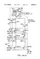
- FIG. 1is a schematic diagram of a typical prior art EEPROM.
- the circuit of FIG. 1allows for flash erasure of all bits stored in the memory array, that is to say the cells are written on a bit-by-bit, or word-by-word basis, the array is read on a word-by-word basis, and the array is erased by erasing all cells simultaneously to the logical one state.
- flash erase EEPROM circuit 100includes a plurality of row lines 101-1 through 101 N, and a plurality of columns or "bit lines" 102-1 through 102-M. Associated with each combination of row line and bit line is one of floating gate memory cell transistors 105-1-1 through 105-N-M.
- each memory cell transistor 105-1-1 through 105-N-Mare connected to their associated row lines 101-1 through 101-N.
- the drains of each memory cell transistorare connected to their associated bit lines.
- the sources of each memory cell transistorare connected in common to the drain of erase transistor 112, as is more fully described later.
- Poweris supplied to each bit line 102-1 through 102-M through column select transistors 104-1 through 104-M, each receiving an appropriate column select signal on their gate leads 103-1 through 103-M, respectively.
- the entire block of array transistors 105-1-1 through 105-N-Mis selected by block transistor 106 receiving a block select signal (for example, a decoded signal based on one or more most significant address bits, with the least significant address bits defining individual memory cells within the block) applied to its gate lead 107.
- a block select signalfor example, a decoded signal based on one or more most significant address bits, with the least significant address bits defining individual memory cells within the block
- block select transistor 106When block select transistor 106 is turned on, the block containing memory cells 105-1-1 through 105-N-M is selected and when one or more column select transistors 104-1 through 104-M are turned on, desired ones of bit lines 102-1 through 102-M are selected. This enables the appropriate voltages to be applied to desired ones of
- a programming voltage VPP(typically 12 volts during programming and 17 volts during erasure) is selectively applied to selected bit lines when programming/erase control circuitry 119 provides a signal to the gate of programming/erase transistor 108 causing transistor 108 to conduct.
- VPPprogramming voltage
- the voltage level of a selected bit lineis applied via transistor 110 to sense amplifier 111 in order to determine the value of the bit stored in a selected memory cell.
- circuit 100in the programming, reading, and erasure modes is depicted in Table 1.
- memory array transistorsare written individually by selectively addressing desired rows and columns.
- a selected rowreceives a voltage (typically approximately 14 volts) thereby enabling the memory transistors within the row to turn on.
- deselected rowseach receive a logical zero, preventing the memory transistors of the deselected rows from turning on.
- their associated bit linesreceive a logical zero by causing their associated column select transistors 104-1 through 104-M to remain off.
- columns whose memory cells are to store a logical oneare deselected.
- columns associated with memory cells which are to store a logical zeroare selected by turning on their associated column select transistors 104-1 through 104-M, and programming/erase control circuitry 119 causes transistor 108 to turn on, thereby applying programming voltage VPP to the selected columns.
- This actioncauses the memory transistors which are to store a logical one to turn on and, with a relatively high voltage VPP applied to their drains, 0 volts on their sources, and a high voltage (typically 14 volts) applied to the control gate, cause hot electrons to be injected from the drain to the floating gate, thereby increasing the control gate threshold voltage to that threshold voltage associated with a logical zero.
- row line 101-1is selected by applying voltage VCC of approximately 5 volts with row lines 101-2 through 101-N being deselected by applying zero volts.
- Bit line 102-1is selected by causing column select transistor 104-1 to turn on, while deselecting bit lines 102-2 through 102-M by causing column select transistors 104-2 through 104-M to be turned off.
- programming/erase transistor 108is turned off, and a reference voltage VREF (typically 2.5 volts) is applied to the gate of pass transistor 110. This causes the voltage on the selected bit line 102-1 to be applied to the input lead of sense amplifier 111, which in turn provides an output signal indicating whether the selected memory cell 105-1-1 stores a logical zero or a logical one.
- VREFtypically 2.5 volts
- memory cell 105-1-1When memory cell 105-1-1 stores a logical one, its control gate threshold voltage is less than the read voltage applied to row line 101-1, and thus memory cell transistor 105-1-1 is turned on pulling the input lead of sense amplifier 111 low through transistors 110, 106, 104-1, 105-1-1, and 112. Conversely, when memory cell 105-1-1 stores a logical zero, its control gate threshold voltage is greater than the read voltage applied to row line 101-1, memory cell transistor 105-1-1 does not turn on, and the input lead of sense amplifier 111 is not pulled low. Thus, sense amplifier 111 can detect the two possible values of the bits stored by the memory selected for reading.
- memory cells 105-1-1 through 105-N-Mare "flash" erased, i.e., all erased simultaneously such that they store logical zeros. This is accomplished by applying 0 volts to the row lines connected to the control gates of the memory transistors, a high voltage (typically 17 volts) to the bit lines connected to the drains of the memory cell transistors, and leaving the erase line, which is connected to the sources of the memory cell transistors, floating.
- a relatively high voltage VPPis applied to selected bit lines 102-1 through 102-M.
- a gated diodeis a PN junction located under the gate electrode.
- the breakdown voltage of the gated diodeis much lower than the breakdown voltage of the gated diode when the gate is not grounded. Furthermore, the gated diode breakdown voltage is lower with thinner gate oxides and shallower junctions depths.
- these transistorsare typically formed utilizing a relatively thick gate oxide (typically 350 ⁇ thick) as compared with the relatively thin gate oxide utilized by the peripheral transistors in the speed path, such as the transistors (not shown) of sense amplifier 111, and the transistors of the address buffers, also not shown, which typically have gate oxide thicknesses on the order of 250 ⁇ .
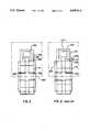
- FIG. 2is a top view of a pair of typical prior art EEPROM memory cells including N+ drain diffusion 201, which is connected via electrical contact 202 to metallization layer 203.
- Cell 200also includes a first layer of polycrystalline silicon 204 which serves as the floating gate of the EEPROM memory transistor, and a second layer of polycrystalline silicon 205 which serves as the control gate and which forms part of a row line.
- programming, reading, and erasure of cell 200is all performed from the drain 201 side of the memory cell.
- speed of an EEPROM deviceis enhanced by utilizing a unique circuit design and operating method which obviates the need for applying a high programming or erase voltage in the path between the memory array and sense amplifier.
- high programming and erase voltagesare applied, as needed, directly to the memory array, thereby allowing all transistors which carry signals from the memory array to the sense amplifier to be fabricated as low voltage devices, thereby increasing their speed of operation and thus the speed of operation of the memory device as a whole.
- FIG. 1is a schematic diagram of a typical prior art flash erase EEPROM device
- FIG. 2is a plan view of a typical prior art EEPROM cell
- FIG. 3is a plan view of an EEPROM cell constructed in accordance with the teachings of this invention.
- FIG. 4is a schematic diagram of one embodiment of a flash erase EEPROM constructed in accordance with the teaching of this invention.
- FIG. 5is a schematic diagram of another embodiment of a flash erase EEPROM constructed in accordance with the teachings of this invention.
- FIG. 4is a schematic diagram of one embodiment of a memory device 400 constructed in accordance with the teachings of this invention.
- FIG. 3is a plan view of a pair of EEPROM memory cells constructed in accordance with the teachings of this invention in which a first layer P1 of polycrystalline silicon forms floating gate 304 located near source 306, rather than near drain 301.
- readingis performed from the drain 301 side of memory cell 300, and programming and erasing performed from the source 306 side of memory cell 300.
- memory device 400includes row lines 401-1 through 401-N, bit lines 402-1 through 402-M, column select transistors 104-1 through 104-M, and memory array transistors 405-1-1 through 405-N-M.
- Block select transistor 406is utilized to access the block of memory cells 405-1-1 through 405-N-M.
- memory cell transistors 405-1-1 through 405-N-Mare fabricated such that their floating gates are located near their sources, rather than near their drains.
- V DSATdrain saturation voltage
- V DSATthe drain saturation voltage
- V GSthe gate-to-source voltage
- V Tthe threshold voltage
- the read currentis limited by the floating gate voltage, which is typically 60 to 70% of the control gate voltage.
- the floating gate voltagetypically 60 to 70% of the control gate voltage.
- the read current through the selected memory cell during the read operationis increased since the saturation voltage V DSAT is increased since the drain is influenced by the control gate voltage, rather than the lesser floating gate voltage.
- reading speedis increased. It has been determined that placing the floating gate near the source rather than near the drain increases the read current by about 10 to 15 percent.
- increased speedis also provided due to the fact that column read voltages may be increased, thereby additionally providing increased read current through a selected array transistor, without risking undesirable "soft" writes of the memory cell being read, since the higher read voltage is applied to the drain which is not located near the floating gate.
- undesirable chargingmay cause a cumulative charge to be placed on the floating gate of a deselected transistor, thereby causing a "soft" write.
- P+ (e.g., Boron) ion implantsneed not be made to the drains of the memory array transistors as is often the case in prior art structures for enhancing the ability to program the cell, since having a P+N+ junction rather than a P-N+ junction increases the maximum field at the junction leading to greater hot electron generation.
- ion implantscan be used on the source side of the memory array transistors where, in accordance with the teachings of this invention, programming occurs by charging the floating gate. By avoiding ion implants on the drains of the memory array transistors, bit line capacitance is reduced, thereby increasing reading speed.
- the P type field implantis not performed near the source of the memory cell transistors, thus increasing the gated diode breakdown voltage of the source junction, which in turn allows greater voltages to be applied to the source in order to improve the performance of the Fowler Nordheim electron tunneling between the source and the floating gate, as well as decreasing susceptibility of the junction to breakdown.
- Fowler Nordheim tunnelingis independent of temperature and is effective only at high electric fields (typically 7 to 10 Megavolts per centimeter).
- Programming of a selected memory array transistoris performed by applying programming voltage VPP to a selected row line while holding deselected row lines at zero volts, and applying programming voltage VPP through transistor 443 to the sources of all memory array transistors.
- a selected columnis grounded by turning on its associated column select transistor, and block select transistor 406 and transistor 421. This causes electrons to be tunneled from the source to the floating gate of the selected transistor.
- programming set transistors 432-1 through 432-M and programming reset transistors 423-1 through 423-Mare utilized to minimize the potential for soft programming cells along the selected row line but along deselected columns, which are left floating and thus may be undesirably charged by current flowing from its source to its drain.
- such soft writingis avoided by precharging the deselected bit lines, thereby preventing current from flowing through deselected memory array transistors, which in turn prevents any amount of charging of the floating gates of deselected transistors during the programming of a selected memory array transistor.
- programming a selected memory array cellfor example transistor 405-1-1, is performed by first applying a PRGSET signal to lead 432, thus turning on precharge transistors 432-1 through 432-M which apply a predefined voltage (for example, 10 volts) to bit lines 402-1 through 402-M, respectively.
- the PRGSET signalthen goes low, turning off transistors 432-1 through 432-M while leaving bit lines 402-1 through 402-M precharged.
- Transistor 421is then turned on, thereby causing selected bit line 402-1 to be discharged through conducting column select transistor 104-1 and block select transistor 406.
- the deselected columns 402-2 through 402-Mremain precharged since their column select transistors 104-2 through 104-M are turned off.
- Source pull down transistor 442is turned off, and programming voltage VPP is applied through transistor 443 to the sources of all memory array transistors 405-1-1 through 405-N-M.
- Selected memory array transistor 405-1-1conducts current from its source to its drain, thereby placing a charge on its floating gate.
- bit lines 402-2 through 402-Mare discharged by applying a PRG reset signal to lead 422, thus turning on reset transistors 423-1 through 423 M.
- reset transistors 423-1 through 423-Mare not used, and the bit lines are discharged by enabling all column select transistors 104-1 through 104-M while transistor 421 is turned on.
Landscapes
- Non-Volatile Memory (AREA)
- Read Only Memory (AREA)
- Semiconductor Memories (AREA)
Abstract
Description
V.sub.DSAT ≃V.sub.GS -V.sub.T ;
TABLE 1 ______________________________________ Programming Row line (control gate) selected: 14 volts deselected: 0 volts bit line (drain) logical 1: 0 volts (column deselected) logical 0: VPP = 9 volts (column selected) erase line (source): 0 volts Reading Row line (control gate) selected: VCC (5 volts) deselected: 0 volts bit line (drain) precharged to V.sub.ref -V.sub.T (typically 1.5 volts) logical 0 stored: pulled low by array transistor, by at least 0.2 volts from pre- charged level logical 0 stored: not pulled low by array transistor erase line (source): 0 volts Erasure Row line (control gate): 0 volts bit line (drain): 17 volts erase line (source): Floating ______________________________________
TABLE 2 ______________________________________ Programming Row line (control gate) selected: VPP = 14 volts deselected: 0 volts bit line (drain) logical 0: selected: approximately 0 volts deselected: approximately 9 volts volts logical 1: 0 volts erase line (source): VSP = 9 volts Reading Row line (control gate) selected: VCC (5 volts) deselected: 0 bit line (drain) logical 0 stored: 2 volts logical 1 stored: 1.8 volts erase line (source): 0 Erasure Row line (control gate): 0 volts bit line (drain): Floating erase line (source): VEE = 17 volts ______________________________________
Claims (21)
Priority Applications (4)
| Application Number | Priority Date | Filing Date | Title |
|---|---|---|---|
| US07/275,380US4999812A (en) | 1988-11-23 | 1988-11-23 | Architecture for a flash erase EEPROM memory |
| EP19890121391EP0370416A3 (en) | 1988-11-23 | 1989-11-18 | Novel architecture for a flash erase eprom memory |
| KR1019890016950AKR0155357B1 (en) | 1988-11-23 | 1989-11-22 | New Structure for Flash Erasing Epiromem Memory |
| JP1303482AJPH03155667A (en) | 1988-11-23 | 1989-11-24 | New architecture for flash erasable eprom memory |
Applications Claiming Priority (1)
| Application Number | Priority Date | Filing Date | Title |
|---|---|---|---|
| US07/275,380US4999812A (en) | 1988-11-23 | 1988-11-23 | Architecture for a flash erase EEPROM memory |
Publications (1)
| Publication Number | Publication Date |
|---|---|
| US4999812Atrue US4999812A (en) | 1991-03-12 |
Family
ID=23052047
Family Applications (1)
| Application Number | Title | Priority Date | Filing Date |
|---|---|---|---|
| US07/275,380Expired - Fee RelatedUS4999812A (en) | 1988-11-23 | 1988-11-23 | Architecture for a flash erase EEPROM memory |
Country Status (4)
| Country | Link |
|---|---|
| US (1) | US4999812A (en) |
| EP (1) | EP0370416A3 (en) |
| JP (1) | JPH03155667A (en) |
| KR (1) | KR0155357B1 (en) |
Cited By (26)
| Publication number | Priority date | Publication date | Assignee | Title |
|---|---|---|---|---|
| US5166562A (en)* | 1991-05-09 | 1992-11-24 | Synaptics, Incorporated | Writable analog reference voltage storage device |
| US5241507A (en)* | 1991-05-03 | 1993-08-31 | Hyundai Electronics America | One transistor cell flash memory assay with over-erase protection |
| US5293328A (en)* | 1992-01-15 | 1994-03-08 | National Semiconductor Corporation | Electrically reprogrammable EPROM cell with merged transistor and optiumum area |
| US5376573A (en)* | 1993-12-10 | 1994-12-27 | Advanced Micro Devices, Inc. | Method of making a flash EPROM device utilizing a single masking step for etching and implanting source regions within the EPROM core and redundancy areas |
| US5384743A (en)* | 1992-03-06 | 1995-01-24 | Sgs-Thomson Microelectronics, S.A. | Structure and method for flash eprom memory erasable by sectors |
| US5396458A (en)* | 1991-10-21 | 1995-03-07 | Rohm Co., Ltd. | Semiconductor memory device and method of writing and reading out information for the same |
| US5427963A (en)* | 1993-12-10 | 1995-06-27 | Advanced Micro Devices, Inc. | Method of making a MOS device with drain side channel implant |
| US5430678A (en)* | 1990-10-02 | 1995-07-04 | Kabushiki Kaisha Toshiba | Semiconductor memory having redundant cells |
| US5528537A (en)* | 1993-03-31 | 1996-06-18 | Samsung Electronics Co., Ltd. | Nonvolatile semiconductor memories with a cell structure suitable for a high speed operation and a low power supply voltage |
| US5581485A (en)* | 1994-12-08 | 1996-12-03 | Omni Microelectronics, Inc. | Analog vector distance measuring and vector quantization architecture |
| US5629891A (en)* | 1991-05-09 | 1997-05-13 | Synaptics, Incorporated | Writable analog reference voltage storage device |
| US5677871A (en)* | 1993-07-29 | 1997-10-14 | Sgs-Thomson Microelectronics S.R.L. | Circuit structure for a memory matrix and corresponding manufacturing method |
| US5748529A (en)* | 1995-11-15 | 1998-05-05 | Samsung Electronics Co., Ltd. | Integrated circuit memory devices having direct read capability |
| US5801076A (en)* | 1995-02-21 | 1998-09-01 | Advanced Micro Devices, Inc. | Method of making non-volatile memory device having a floating gate with enhanced charge retention |
| US5828603A (en)* | 1997-04-23 | 1998-10-27 | Atmel Corporation | Memory device having a power supply-independent low power consumption bit line voltage clamp |
| US5898616A (en)* | 1997-05-08 | 1999-04-27 | Oki Electric Industry Co., Ltd. | Semiconductor nonvolatile memory and source circuit for this memory |
| US5920296A (en)* | 1995-02-01 | 1999-07-06 | Pixel International | Flat screen having individually dipole-protected microdots |
| US6031765A (en)* | 1999-04-22 | 2000-02-29 | Aplus Flash Technology, Inc. | Reversed split-gate cell array |
| US6175520B1 (en) | 1997-05-30 | 2001-01-16 | Alliance Semiconductor Corporation | Nonvolatile memory array having local program load line repeaters |
| US6181607B1 (en) | 1999-04-22 | 2001-01-30 | Aplus Flash Technology, Inc. | Reversed split-gate cell array |
| US20040103239A1 (en)* | 2002-11-21 | 2004-05-27 | Micron Technology, Inc. | Preconditioning of defective and redundant columns in a memory device |
| US20050145895A1 (en)* | 2004-01-05 | 2005-07-07 | International Business Machines Corporation | Amplifiers using gated diodes |
| US20060050581A1 (en)* | 2004-09-03 | 2006-03-09 | International Business Machines Corporation | Sense amplifier circuits and high speed latch circuits using gated diodes |
| US20090307140A1 (en)* | 2008-06-06 | 2009-12-10 | Upendra Mardikar | Mobile device over-the-air (ota) registration and point-of-sale (pos) payment |
| US7995384B2 (en) | 2008-08-15 | 2011-08-09 | Macronix International Co., Ltd. | Electrically isolated gated diode nonvolatile memory |
| US11595820B2 (en) | 2011-09-02 | 2023-02-28 | Paypal, Inc. | Secure elements broker (SEB) for application communication channel selector optimization |
Families Citing this family (1)
| Publication number | Priority date | Publication date | Assignee | Title |
|---|---|---|---|---|
| WO2006038249A1 (en)* | 2004-09-30 | 2006-04-13 | Spansion Llc | Semiconductor device and method for controlling the same |
Citations (2)
| Publication number | Priority date | Publication date | Assignee | Title |
|---|---|---|---|---|
| US4462090A (en)* | 1978-12-14 | 1984-07-24 | Tokyo Shibaura Denki Kabushiki Kaisha | Method of operating a semiconductor memory circuit |
| US4852062A (en)* | 1987-09-28 | 1989-07-25 | Motorola, Inc. | EPROM device using asymmetrical transistor characteristics |
Family Cites Families (1)
| Publication number | Priority date | Publication date | Assignee | Title |
|---|---|---|---|---|
| US4698787A (en)* | 1984-11-21 | 1987-10-06 | Exel Microelectronics, Inc. | Single transistor electrically programmable memory device and method |
- 1988
- 1988-11-23USUS07/275,380patent/US4999812A/ennot_activeExpired - Fee Related
- 1989
- 1989-11-18EPEP19890121391patent/EP0370416A3/ennot_activeWithdrawn
- 1989-11-22KRKR1019890016950Apatent/KR0155357B1/ennot_activeExpired - Fee Related
- 1989-11-24JPJP1303482Apatent/JPH03155667A/enactivePending
Patent Citations (2)
| Publication number | Priority date | Publication date | Assignee | Title |
|---|---|---|---|---|
| US4462090A (en)* | 1978-12-14 | 1984-07-24 | Tokyo Shibaura Denki Kabushiki Kaisha | Method of operating a semiconductor memory circuit |
| US4852062A (en)* | 1987-09-28 | 1989-07-25 | Motorola, Inc. | EPROM device using asymmetrical transistor characteristics |
Cited By (41)
| Publication number | Priority date | Publication date | Assignee | Title |
|---|---|---|---|---|
| US5430678A (en)* | 1990-10-02 | 1995-07-04 | Kabushiki Kaisha Toshiba | Semiconductor memory having redundant cells |
| US5241507A (en)* | 1991-05-03 | 1993-08-31 | Hyundai Electronics America | One transistor cell flash memory assay with over-erase protection |
| US5629891A (en)* | 1991-05-09 | 1997-05-13 | Synaptics, Incorporated | Writable analog reference voltage storage device |
| US5166562A (en)* | 1991-05-09 | 1992-11-24 | Synaptics, Incorporated | Writable analog reference voltage storage device |
| US5396458A (en)* | 1991-10-21 | 1995-03-07 | Rohm Co., Ltd. | Semiconductor memory device and method of writing and reading out information for the same |
| US5293328A (en)* | 1992-01-15 | 1994-03-08 | National Semiconductor Corporation | Electrically reprogrammable EPROM cell with merged transistor and optiumum area |
| US5455793A (en)* | 1992-01-15 | 1995-10-03 | National Semiconductor Corp. | Electrically reprogrammable EPROM cell with merged transistor and optimum area |
| US5384743A (en)* | 1992-03-06 | 1995-01-24 | Sgs-Thomson Microelectronics, S.A. | Structure and method for flash eprom memory erasable by sectors |
| US5635747A (en)* | 1993-03-31 | 1997-06-03 | Samsung Electronics Co., Ltd. | Nonvolatile semiconductor memories with a cell structure suitable for a high speed operation and a low power supply voltage |
| US5528537A (en)* | 1993-03-31 | 1996-06-18 | Samsung Electronics Co., Ltd. | Nonvolatile semiconductor memories with a cell structure suitable for a high speed operation and a low power supply voltage |
| US5677871A (en)* | 1993-07-29 | 1997-10-14 | Sgs-Thomson Microelectronics S.R.L. | Circuit structure for a memory matrix and corresponding manufacturing method |
| US5376573A (en)* | 1993-12-10 | 1994-12-27 | Advanced Micro Devices, Inc. | Method of making a flash EPROM device utilizing a single masking step for etching and implanting source regions within the EPROM core and redundancy areas |
| US5427963A (en)* | 1993-12-10 | 1995-06-27 | Advanced Micro Devices, Inc. | Method of making a MOS device with drain side channel implant |
| US5581485A (en)* | 1994-12-08 | 1996-12-03 | Omni Microelectronics, Inc. | Analog vector distance measuring and vector quantization architecture |
| US5920296A (en)* | 1995-02-01 | 1999-07-06 | Pixel International | Flat screen having individually dipole-protected microdots |
| US5801076A (en)* | 1995-02-21 | 1998-09-01 | Advanced Micro Devices, Inc. | Method of making non-volatile memory device having a floating gate with enhanced charge retention |
| US5805013A (en)* | 1995-02-21 | 1998-09-08 | Advanced Micro Devices, Inc. | Non-volatile memory device having a floating gate with enhanced charge retention |
| US5748529A (en)* | 1995-11-15 | 1998-05-05 | Samsung Electronics Co., Ltd. | Integrated circuit memory devices having direct read capability |
| US5828603A (en)* | 1997-04-23 | 1998-10-27 | Atmel Corporation | Memory device having a power supply-independent low power consumption bit line voltage clamp |
| US5898616A (en)* | 1997-05-08 | 1999-04-27 | Oki Electric Industry Co., Ltd. | Semiconductor nonvolatile memory and source circuit for this memory |
| US6175520B1 (en) | 1997-05-30 | 2001-01-16 | Alliance Semiconductor Corporation | Nonvolatile memory array having local program load line repeaters |
| US6031765A (en)* | 1999-04-22 | 2000-02-29 | Aplus Flash Technology, Inc. | Reversed split-gate cell array |
| US6181607B1 (en) | 1999-04-22 | 2001-01-30 | Aplus Flash Technology, Inc. | Reversed split-gate cell array |
| US7145800B2 (en) | 2002-11-21 | 2006-12-05 | Micron Technology, Inc. | Preconditioning of defective and redundant columns in a memory device |
| US20040103239A1 (en)* | 2002-11-21 | 2004-05-27 | Micron Technology, Inc. | Preconditioning of defective and redundant columns in a memory device |
| US6977841B2 (en)* | 2002-11-21 | 2005-12-20 | Micron Technology, Inc. | Preconditioning of defective and redundant columns in a memory device |
| US20060034126A1 (en)* | 2002-11-21 | 2006-02-16 | Micron Technology, Inc. | Preconditioning of defective and redundant columns in a memory device |
| US8324667B2 (en)* | 2004-01-05 | 2012-12-04 | International Business Machines Corporation | Amplifiers using gated diodes |
| US8941412B2 (en) | 2004-01-05 | 2015-01-27 | International Business Machines Corporation | Amplifiers using gated diodes |
| US8120386B2 (en)* | 2004-01-05 | 2012-02-21 | International Business Machines Corporation | Amplifiers using gated diodes |
| US20090302936A1 (en)* | 2004-01-05 | 2009-12-10 | International Business Machines Corporation | Amplifiers using gated diodes |
| US20050145895A1 (en)* | 2004-01-05 | 2005-07-07 | International Business Machines Corporation | Amplifiers using gated diodes |
| US20060050581A1 (en)* | 2004-09-03 | 2006-03-09 | International Business Machines Corporation | Sense amplifier circuits and high speed latch circuits using gated diodes |
| US20060255850A1 (en)* | 2004-09-03 | 2006-11-16 | International Business Machines Corporation | High speed latch circuits using gated diodes |
| US7242629B2 (en) | 2004-09-03 | 2007-07-10 | International Business Machines Corporation | High speed latch circuits using gated diodes |
| US7116594B2 (en) | 2004-09-03 | 2006-10-03 | International Business Machines Corporation | Sense amplifier circuits and high speed latch circuits using gated diodes |
| US20090307140A1 (en)* | 2008-06-06 | 2009-12-10 | Upendra Mardikar | Mobile device over-the-air (ota) registration and point-of-sale (pos) payment |
| US11521194B2 (en) | 2008-06-06 | 2022-12-06 | Paypal, Inc. | Trusted service manager (TSM) architectures and methods |
| US7995384B2 (en) | 2008-08-15 | 2011-08-09 | Macronix International Co., Ltd. | Electrically isolated gated diode nonvolatile memory |
| US11595820B2 (en) | 2011-09-02 | 2023-02-28 | Paypal, Inc. | Secure elements broker (SEB) for application communication channel selector optimization |
| US12022290B2 (en) | 2011-09-02 | 2024-06-25 | Paypal, Inc. | Secure elements broker (SEB) for application communication channel selector optimization |
Also Published As
| Publication number | Publication date |
|---|---|
| KR0155357B1 (en) | 1998-12-01 |
| KR900008528A (en) | 1990-06-04 |
| EP0370416A2 (en) | 1990-05-30 |
| EP0370416A3 (en) | 1990-12-05 |
| JPH03155667A (en) | 1991-07-03 |
Similar Documents
| Publication | Publication Date | Title |
|---|---|---|
| US4999812A (en) | Architecture for a flash erase EEPROM memory | |
| US5511022A (en) | Depletion mode NAND string electrically erasable programmable semiconductor memory device and method for erasing and programming thereof | |
| US5596525A (en) | Memory cell of nonvolatile semiconductor memory device | |
| EP0545904B1 (en) | Nonvolatile semiconductor memory device | |
| US5294819A (en) | Single-transistor cell EEPROM array for analog or digital storage | |
| US5812452A (en) | Electrically byte-selectable and byte-alterable memory arrays | |
| US4366555A (en) | Electrically erasable programmable read only memory | |
| US4425632A (en) | Nonvolatile semiconductor memory device | |
| EP0558404A2 (en) | Single transistor flash electrically programmable memory | |
| JPH08279297A (en) | NAND structure non-volatile semiconductor memory and programming method thereof | |
| KR20010030062A (en) | Nonvolatile semiconductor memory | |
| US5521867A (en) | Adjustable threshold voltage conversion circuit | |
| US5912837A (en) | Bitline disturb reduction | |
| US7995399B2 (en) | NAND memory device and programming methods | |
| US7436716B2 (en) | Nonvolatile memory | |
| US5576993A (en) | Flash memory array with self-limiting erase | |
| KR19990014206A (en) | Nonvolatile Semiconductor Memory | |
| US6011717A (en) | EEPROM memory programmable and erasable by Fowler-Nordheim effect | |
| KR19990013057A (en) | Read and write method of flash memory device for selectively storing single bit data and multiple bit data on same chip | |
| US5943268A (en) | Non-volatile latch having PMOS floating gate memory cells | |
| US5544099A (en) | Method of writing data into electrically erasable and programmable read only memory cell without disturbance to other cells | |
| JPH0314272A (en) | Nonvolatile semiconductor storage device | |
| US3781831A (en) | Read only memory utilizing floating gate transistors and method of programming | |
| KR960011187B1 (en) | Non-volatile semiconductor memory using a thin film transistor | |
| US5808940A (en) | Nonvolatile semiconductor memory |
Legal Events
| Date | Code | Title | Description |
|---|---|---|---|
| AS | Assignment | Owner name:NATIONAL SEMICONDUCTOR CORPORATION, CALIFORNIA Free format text:ASSIGNMENT OF ASSIGNORS INTEREST.;ASSIGNOR:AMIN, ALAAELDIN;REEL/FRAME:005039/0284 Effective date:19890118 | |
| FPAY | Fee payment | Year of fee payment:4 | |
| AS | Assignment | Owner name:FAIRCHILD SEMICONDUCTOR CORPORATION, MAINE Free format text:ASSIGNMENT OF ASSIGNORS INTEREST;ASSIGNOR:NATIONAL SEMICONDUCTOR CORPORATION;REEL/FRAME:008535/0103 Effective date:19970311 Owner name:BANKERS TRUST COMPANY, NEW YORK Free format text:SECURITY INTEREST;ASSIGNOR:FAIRCHILD SEMICONDUCTOR CORPORATION;REEL/FRAME:008454/0101 Effective date:19970311 | |
| FEPP | Fee payment procedure | Free format text:PAYOR NUMBER ASSIGNED (ORIGINAL EVENT CODE: ASPN); ENTITY STATUS OF PATENT OWNER: LARGE ENTITY | |
| REMI | Maintenance fee reminder mailed | ||
| FPAY | Fee payment | Year of fee payment:8 | |
| SULP | Surcharge for late payment | ||
| AS | Assignment | Owner name:CREDIT SUISSE FIRST BOSTON, NEW YORK Free format text:SECURITY AGREEMENT;ASSIGNOR:FAIRCHILD SEMICONDUCTOR CORPORATION;REEL/FRAME:009883/0800 Effective date:19990414 | |
| AS | Assignment | Owner name:FAIRCHILD SEMICONDUCTOR CORPORATION, MAINE Free format text:RELEASE BY SECURED PARTY;ASSIGNOR:BANKERS TRUST COMPANY;REEL/FRAME:009901/0528 Effective date:19990414 | |
| AS | Assignment | Owner name:FAIRCHILD SEMICONDUCTOR CORPORATION, MAINE Free format text:RELEASE;ASSIGNOR:CREDIT SUISSE FIRST BOSTON;REEL/FRAME:010996/0537 Effective date:20000602 | |
| LAPS | Lapse for failure to pay maintenance fees | ||
| STCH | Information on status: patent discontinuation | Free format text:PATENT EXPIRED DUE TO NONPAYMENT OF MAINTENANCE FEES UNDER 37 CFR 1.362 | |
| FP | Lapsed due to failure to pay maintenance fee | Effective date:20030312 |