US4997789A - Aluminum contact etch mask and etchstop for tungsten etchback - Google Patents
Aluminum contact etch mask and etchstop for tungsten etchbackDownload PDFInfo
- Publication number
- US4997789A US4997789AUS07/265,162US26516288AUS4997789AUS 4997789 AUS4997789 AUS 4997789AUS 26516288 AUS26516288 AUS 26516288AUS 4997789 AUS4997789 AUS 4997789A
- Authority
- US
- United States
- Prior art keywords
- layer
- metal
- tungsten
- forming
- aluminum
- Prior art date
- Legal status (The legal status is an assumption and is not a legal conclusion. Google has not performed a legal analysis and makes no representation as to the accuracy of the status listed.)
- Expired - Fee Related
Links
- 229910052721tungstenInorganic materials0.000titleclaimsabstractdescription29
- 239000010937tungstenSubstances0.000titleclaimsabstractdescription29
- WFKWXMTUELFFGS-UHFFFAOYSA-NtungstenChemical compound[W]WFKWXMTUELFFGS-UHFFFAOYSA-N0.000titleclaimsabstractdescription28
- 229910052782aluminiumInorganic materials0.000titleclaimsabstractdescription22
- XAGFODPZIPBFFR-UHFFFAOYSA-NaluminiumChemical compound[Al]XAGFODPZIPBFFR-UHFFFAOYSA-N0.000titleclaimsabstractdescription22
- 238000000034methodMethods0.000claimsabstractdescription31
- 238000005530etchingMethods0.000claimsabstractdescription11
- 239000004065semiconductorSubstances0.000claimsabstractdescription10
- 229910052751metalInorganic materials0.000claimsdescription28
- 239000002184metalSubstances0.000claimsdescription28
- 230000004888barrier functionEffects0.000claimsdescription11
- 238000000151depositionMethods0.000claimsdescription8
- 239000000463materialSubstances0.000claimsdescription6
- 238000001465metallisationMethods0.000claimsdescription6
- XUIMIQQOPSSXEZ-UHFFFAOYSA-NSiliconChemical compound[Si]XUIMIQQOPSSXEZ-UHFFFAOYSA-N0.000claimsdescription3
- 230000008021depositionEffects0.000claimsdescription3
- 229910052710siliconInorganic materials0.000claimsdescription3
- 239000010703siliconSubstances0.000claimsdescription3
- RTAQQCXQSZGOHL-UHFFFAOYSA-NTitaniumChemical compound[Ti]RTAQQCXQSZGOHL-UHFFFAOYSA-N0.000claims4
- 239000012212insulatorSubstances0.000claims4
- 239000010936titaniumSubstances0.000claims4
- 229910052719titaniumInorganic materials0.000claims4
- VYPSYNLAJGMNEJ-UHFFFAOYSA-NSilicium dioxideChemical groupO=[Si]=OVYPSYNLAJGMNEJ-UHFFFAOYSA-N0.000claims2
- 229910001080W alloyInorganic materials0.000claims2
- 238000000059patterningMethods0.000claims2
- 229910000838Al alloyInorganic materials0.000claims1
- RYGMFSIKBFXOCR-UHFFFAOYSA-NCopperChemical compound[Cu]RYGMFSIKBFXOCR-UHFFFAOYSA-N0.000claims1
- 229910052802copperInorganic materials0.000claims1
- 239000010949copperSubstances0.000claims1
- 235000012239silicon dioxideNutrition0.000claims1
- 239000000377silicon dioxideSubstances0.000claims1
- MAKDTFFYCIMFQP-UHFFFAOYSA-Ntitanium tungstenChemical compound[Ti].[W]MAKDTFFYCIMFQP-UHFFFAOYSA-N0.000claims1
- 230000015572biosynthetic processEffects0.000abstractdescription4
- 229920002120photoresistant polymerPolymers0.000description9
- 230000008901benefitEffects0.000description7
- 239000000758substrateSubstances0.000description6
- 238000002955isolationMethods0.000description2
- 229910021420polycrystalline siliconInorganic materials0.000description2
- 229920005591polysiliconPolymers0.000description2
- 229910016570AlCuInorganic materials0.000description1
- 229910000881Cu alloyInorganic materials0.000description1
- WPPDFTBPZNZZRP-UHFFFAOYSA-Naluminum copperChemical compound[Al].[Cu]WPPDFTBPZNZZRP-UHFFFAOYSA-N0.000description1
- 238000010420art techniqueMethods0.000description1
- 238000007796conventional methodMethods0.000description1
- 238000005516engineering processMethods0.000description1
- 238000007689inspectionMethods0.000description1
- 230000010354integrationEffects0.000description1
- 238000004519manufacturing processMethods0.000description1
- 238000005259measurementMethods0.000description1
- JTJMJGYZQZDUJJ-UHFFFAOYSA-NphencyclidineChemical compoundC1CCCCN1C1(C=2C=CC=CC=2)CCCCC1JTJMJGYZQZDUJJ-UHFFFAOYSA-N0.000description1
- 229920000642polymerPolymers0.000description1
- 238000002360preparation methodMethods0.000description1
- 230000003449preventive effectEffects0.000description1
Images


Classifications
- H—ELECTRICITY
- H01—ELECTRIC ELEMENTS
- H01L—SEMICONDUCTOR DEVICES NOT COVERED BY CLASS H10
- H01L21/00—Processes or apparatus adapted for the manufacture or treatment of semiconductor or solid state devices or of parts thereof
- H01L21/70—Manufacture or treatment of devices consisting of a plurality of solid state components formed in or on a common substrate or of parts thereof; Manufacture of integrated circuit devices or of parts thereof
- H01L21/71—Manufacture of specific parts of devices defined in group H01L21/70
- H01L21/768—Applying interconnections to be used for carrying current between separate components within a device comprising conductors and dielectrics
- H01L21/76838—Applying interconnections to be used for carrying current between separate components within a device comprising conductors and dielectrics characterised by the formation and the after-treatment of the conductors
- H01L21/7684—Smoothing; Planarisation
- H—ELECTRICITY
- H01—ELECTRIC ELEMENTS
- H01L—SEMICONDUCTOR DEVICES NOT COVERED BY CLASS H10
- H01L21/00—Processes or apparatus adapted for the manufacture or treatment of semiconductor or solid state devices or of parts thereof
- H01L21/02—Manufacture or treatment of semiconductor devices or of parts thereof
- H01L21/04—Manufacture or treatment of semiconductor devices or of parts thereof the devices having potential barriers, e.g. a PN junction, depletion layer or carrier concentration layer
- H01L21/18—Manufacture or treatment of semiconductor devices or of parts thereof the devices having potential barriers, e.g. a PN junction, depletion layer or carrier concentration layer the devices having semiconductor bodies comprising elements of Group IV of the Periodic Table or AIIIBV compounds with or without impurities, e.g. doping materials
- H01L21/30—Treatment of semiconductor bodies using processes or apparatus not provided for in groups H01L21/20 - H01L21/26
- H01L21/31—Treatment of semiconductor bodies using processes or apparatus not provided for in groups H01L21/20 - H01L21/26 to form insulating layers thereon, e.g. for masking or by using photolithographic techniques; After treatment of these layers; Selection of materials for these layers
- H01L21/3205—Deposition of non-insulating-, e.g. conductive- or resistive-, layers on insulating layers; After-treatment of these layers
- H01L21/321—After treatment
- H01L21/3213—Physical or chemical etching of the layers, e.g. to produce a patterned layer from a pre-deposited extensive layer
- H01L21/32139—Physical or chemical etching of the layers, e.g. to produce a patterned layer from a pre-deposited extensive layer using masks
- H—ELECTRICITY
- H01—ELECTRIC ELEMENTS
- H01L—SEMICONDUCTOR DEVICES NOT COVERED BY CLASS H10
- H01L21/00—Processes or apparatus adapted for the manufacture or treatment of semiconductor or solid state devices or of parts thereof
- H01L21/70—Manufacture or treatment of devices consisting of a plurality of solid state components formed in or on a common substrate or of parts thereof; Manufacture of integrated circuit devices or of parts thereof
- H01L21/71—Manufacture of specific parts of devices defined in group H01L21/70
- H01L21/768—Applying interconnections to be used for carrying current between separate components within a device comprising conductors and dielectrics
- H01L21/76838—Applying interconnections to be used for carrying current between separate components within a device comprising conductors and dielectrics characterised by the formation and the after-treatment of the conductors
- H01L21/76841—Barrier, adhesion or liner layers
- H—ELECTRICITY
- H01—ELECTRIC ELEMENTS
- H01L—SEMICONDUCTOR DEVICES NOT COVERED BY CLASS H10
- H01L21/00—Processes or apparatus adapted for the manufacture or treatment of semiconductor or solid state devices or of parts thereof
- H01L21/70—Manufacture or treatment of devices consisting of a plurality of solid state components formed in or on a common substrate or of parts thereof; Manufacture of integrated circuit devices or of parts thereof
- H01L21/71—Manufacture of specific parts of devices defined in group H01L21/70
- H01L21/768—Applying interconnections to be used for carrying current between separate components within a device comprising conductors and dielectrics
- H01L21/76838—Applying interconnections to be used for carrying current between separate components within a device comprising conductors and dielectrics characterised by the formation and the after-treatment of the conductors
- H01L21/76877—Filling of holes, grooves or trenches, e.g. vias, with conductive material
- Y—GENERAL TAGGING OF NEW TECHNOLOGICAL DEVELOPMENTS; GENERAL TAGGING OF CROSS-SECTIONAL TECHNOLOGIES SPANNING OVER SEVERAL SECTIONS OF THE IPC; TECHNICAL SUBJECTS COVERED BY FORMER USPC CROSS-REFERENCE ART COLLECTIONS [XRACs] AND DIGESTS
- Y10—TECHNICAL SUBJECTS COVERED BY FORMER USPC
- Y10S—TECHNICAL SUBJECTS COVERED BY FORMER USPC CROSS-REFERENCE ART COLLECTIONS [XRACs] AND DIGESTS
- Y10S438/00—Semiconductor device manufacturing: process
- Y10S438/942—Masking
- Y10S438/945—Special, e.g. metal
Definitions
- the present inventionrelates generally to semiconductor etching techniques and more particularly to using aluminum as an etch mask and etchstop for tungsten etchback.
- the present inventioncomprises a method for using aluminum as an etchstop in the process for forming CVD tungsten filled contacts.
- the aluminum etchstopmay also be used as a mask during the contact/via etch prior to the non-selective CVD tungsten deposition. This technique has several advantages over the conventional use of a photoresist mask.
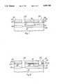
- FIGS. 1-5depict cross-sectional views showing various stages in a preferred embodiment of the present method for utilizing aluminum as an etch-stop.
- FIG. 1illustrates an intermediate step in the present inventive process.
- the FIG. 1 struture 10comprises a conventional silicon substrate 12 having active moat area isolation oxide regions 14a-b. Overlying a portion of oxide isolation region 14b is a polysilicon emitter 18 having oxide sidewall 16. Although the structure is illustrated as a bipolar device, the teachings of the present invention are compatible with FET and BICMOS technologies. Disposed over substrate 12 is a layer of field oxide 20. Oxide layer 20 shown is pre-metal planarized or via planarized in preparation for contact/via formation in accordance with the teachings of the present invention.
- a conventional titaninum-tungsten TiW, or other barrier metal, layer 22is disposed on the planar oxide surface.
- the preferred thickness of the barrier layeris approximately 200 nanometers.
- layer 22can be formed in the range of 0 to 400 nanometers.
- a thinner TiW layerhelps to prevent undercutting of the TiW beneath the aluminum during the metal or oxide etch.
- Disposed on barrier layer 22is approximately 200 to 300 nanometers of an aluminum or aluminum-copper alloy 24. In prior art techniques this is the metallization layer and is conventionally deposited to approximately 700 nanometers.
- the contacts or viasare patterned and etched using conventional and well known photoresist/photolithographic techniques.
- the resist materialis identified by reference numeral 26.
- the AlCu and TiW layersare etched in the exposed regions to the level of oxide layer 20 to define contact/via openings such as 28 and 30.
- the photoresist materialmay be stripped at this time and the substrate may be inspected to ensure that no missing or closing contacts or vias are present. If such detriments do exist it is easier to strip the metal, redeposit, repattern and reetch at.
- oxide layer 20is now ready for etching.
- photoresist layer 26can be removed and aluminum layer 24 will then serve as an etch mask.
- oxide layer 20is shown etched to the surface of silicon layer 12 in contact 28 and to the surface of polysilicon layer 18 in via opening 30. As shown in FIG. 3, the remaining photoresist material 26 has been removed and a conformal layer of tungsten 32 is shown disposed over the substrate filling respective vias 28 and 30.
- a TiW "sticky layer"(not shown) of approximately 50 nanometers may be deposited over the oxide in the via openings 28 and 30 to ensure that the W will adhere to the oxide surfaces of the contact openings.
- a post tungsten deposition resist etchbackhas been performed on the substrate.
- the resist etchbackplanarizes the wafer surface, removing the W disposed on the surface of the aluminum layer.
- Over etching of the tungsten contacts into oxide layer 20is prevented as heretofore mentioned because aluminum layer 24 additionally acts as an etch stop for the etching process.
- barrier layercan be formed without the requirement that other preventive measures be taken to prevent over etching. If after the etching step the aluminum is in an acceptable condition, i.e., is not damaged and may be used for metallization, the remaining amount of aluminum 34 required for metallization may be deposited directly over aluminum layer 24, as shown in FIG. 5. If Al layer 24 is unacceptable it may be removed by such conventional techniques as an Al leach, Sherman etch, etc., down to barrier layer 22. Then the conventional metallization thickness of approximately 700 nanometers may be deposited.
- the aluminumcould be stripped after the tungsten resist etchback and an additional amount of TiW could be deposited to correct any undercutting which may have occurred. Thereafter the aluminum can be replaced for lead definition.
- Another technical advantage of the invention presentedis that it facilitates inspection for missing or closing contacts thus allowing better opportunity for reworking the substrate. Additionally, the contacts formed in accordance with the present method have less flaring at the tops thereof.
- Yet another technical advantage of the present inventive methodis that high selectivity between tungsten/TiW and oxide is no longer required. Thus tungsten resist etchback is performed without thinning the CVD oxide layer over the active devices. By using the present method precise measurement of the amount of metal remaining over the CVD oxide after the planarization is not required.
Landscapes
- Engineering & Computer Science (AREA)
- Physics & Mathematics (AREA)
- Condensed Matter Physics & Semiconductors (AREA)
- General Physics & Mathematics (AREA)
- Manufacturing & Machinery (AREA)
- Computer Hardware Design (AREA)
- Microelectronics & Electronic Packaging (AREA)
- Power Engineering (AREA)
- Internal Circuitry In Semiconductor Integrated Circuit Devices (AREA)
Abstract
Description
Claims (9)
Priority Applications (1)
| Application Number | Priority Date | Filing Date | Title |
|---|---|---|---|
| US07/265,162US4997789A (en) | 1988-10-31 | 1988-10-31 | Aluminum contact etch mask and etchstop for tungsten etchback |
Applications Claiming Priority (1)
| Application Number | Priority Date | Filing Date | Title |
|---|---|---|---|
| US07/265,162US4997789A (en) | 1988-10-31 | 1988-10-31 | Aluminum contact etch mask and etchstop for tungsten etchback |
Publications (1)
| Publication Number | Publication Date |
|---|---|
| US4997789Atrue US4997789A (en) | 1991-03-05 |
Family
ID=23009283
Family Applications (1)
| Application Number | Title | Priority Date | Filing Date |
|---|---|---|---|
| US07/265,162Expired - Fee RelatedUS4997789A (en) | 1988-10-31 | 1988-10-31 | Aluminum contact etch mask and etchstop for tungsten etchback |
Country Status (1)
| Country | Link |
|---|---|
| US (1) | US4997789A (en) |
Cited By (15)
| Publication number | Priority date | Publication date | Assignee | Title |
|---|---|---|---|---|
| US5164330A (en)* | 1991-04-17 | 1992-11-17 | Intel Corporation | Etchback process for tungsten utilizing a NF3/AR chemistry |
| US5225040A (en)* | 1990-04-16 | 1993-07-06 | Raytheon Company | Process for patterning metal connections in small-geometry semiconductor structures |
| US5252516A (en)* | 1992-02-20 | 1993-10-12 | International Business Machines Corporation | Method for producing interlevel stud vias |
| US5372971A (en)* | 1991-10-02 | 1994-12-13 | Hyundai Electronics Industries Co. Ltd. | Method for forming via hole in multiple metal layers of semiconductor device |
| US5466639A (en)* | 1994-10-06 | 1995-11-14 | Micron Semiconductor, Inc. | Double mask process for forming trenches and contacts during the formation of a semiconductor memory device |
| US5534462A (en)* | 1995-02-24 | 1996-07-09 | Motorola, Inc. | Method for forming a plug and semiconductor device having the same |
| US5897374A (en)* | 1995-05-22 | 1999-04-27 | Taiwan Semiconductor Manufacturing Company, Ltd. | Vertical via/contact with undercut dielectric |
| US5948700A (en)* | 1996-05-20 | 1999-09-07 | Chartered Semiconductor Manufacturing Ltd. | Method of planarization of an intermetal dielectric layer using chemical mechanical polishing |
| US5989784A (en)* | 1998-04-06 | 1999-11-23 | Taiwan Semiconductor Manufacturing Company, Ltd. | Etch recipe for embedded DRAM passivation with etch stopping layer scheme |
| US6016008A (en)* | 1995-03-30 | 2000-01-18 | Siemens Aktiengesellschaft | Integrated circuit interconnection employing tungsten/aluminum layers |
| US6028363A (en)* | 1997-06-04 | 2000-02-22 | Taiwan Semiconductor Manufacturing Company | Vertical via/contact |
| US6069051A (en)* | 1996-06-17 | 2000-05-30 | International Business Machines Corporation | Method of producing planar metal-to-metal capacitor for use in integrated circuits |
| US6124189A (en)* | 1997-03-14 | 2000-09-26 | Kabushiki Kaisha Toshiba | Metallization structure and method for a semiconductor device |
| US6414392B1 (en)* | 1992-07-28 | 2002-07-02 | Micron Technology, Inc. | Integrated circuit contact |
| US20060079072A1 (en)* | 2004-10-08 | 2006-04-13 | Ludwig David | Method for precision integrated circuit die singulation using differential etch rates |
Citations (13)
| Publication number | Priority date | Publication date | Assignee | Title |
|---|---|---|---|---|
| US4184909A (en)* | 1978-08-21 | 1980-01-22 | International Business Machines Corporation | Method of forming thin film interconnection systems |
| US4367119A (en)* | 1980-08-18 | 1983-01-04 | International Business Machines Corporation | Planar multi-level metal process with built-in etch stop |
| US4517225A (en)* | 1983-05-02 | 1985-05-14 | Signetics Corporation | Method for manufacturing an electrical interconnection by selective tungsten deposition |
| US4630357A (en)* | 1985-08-02 | 1986-12-23 | Ncr Corporation | Method for forming improved contacts between interconnect layers of an integrated circuit |
| US4631806A (en)* | 1985-05-22 | 1986-12-30 | Gte Laboratories Incorporated | Method of producing integrated circuit structures |
| US4666737A (en)* | 1986-02-11 | 1987-05-19 | Harris Corporation | Via metallization using metal fillets |
| US4670091A (en)* | 1984-08-23 | 1987-06-02 | Fairchild Semiconductor Corporation | Process for forming vias on integrated circuits |
| US4721689A (en)* | 1986-08-28 | 1988-01-26 | International Business Machines Corporation | Method for simultaneously forming an interconnection level and via studs |
| US4753709A (en)* | 1987-02-05 | 1988-06-28 | Texas Instuments Incorporated | Method for etching contact vias in a semiconductor device |
| US4789648A (en)* | 1985-10-28 | 1988-12-06 | International Business Machines Corporation | Method for producing coplanar multi-level metal/insulator films on a substrate and for forming patterned conductive lines simultaneously with stud vias |
| US4808552A (en)* | 1985-09-11 | 1989-02-28 | Texas Instruments Incorporated | Process for making vertically-oriented interconnections for VLSI devices |
| US4824802A (en)* | 1986-02-28 | 1989-04-25 | General Electric Company | Method of filling interlevel dielectric via or contact holes in multilevel VLSI metallization structures |
| US4855252A (en)* | 1988-08-22 | 1989-08-08 | International Business Machines Corporation | Process for making self-aligned contacts |
- 1988
- 1988-10-31USUS07/265,162patent/US4997789A/ennot_activeExpired - Fee Related
Patent Citations (13)
| Publication number | Priority date | Publication date | Assignee | Title |
|---|---|---|---|---|
| US4184909A (en)* | 1978-08-21 | 1980-01-22 | International Business Machines Corporation | Method of forming thin film interconnection systems |
| US4367119A (en)* | 1980-08-18 | 1983-01-04 | International Business Machines Corporation | Planar multi-level metal process with built-in etch stop |
| US4517225A (en)* | 1983-05-02 | 1985-05-14 | Signetics Corporation | Method for manufacturing an electrical interconnection by selective tungsten deposition |
| US4670091A (en)* | 1984-08-23 | 1987-06-02 | Fairchild Semiconductor Corporation | Process for forming vias on integrated circuits |
| US4631806A (en)* | 1985-05-22 | 1986-12-30 | Gte Laboratories Incorporated | Method of producing integrated circuit structures |
| US4630357A (en)* | 1985-08-02 | 1986-12-23 | Ncr Corporation | Method for forming improved contacts between interconnect layers of an integrated circuit |
| US4808552A (en)* | 1985-09-11 | 1989-02-28 | Texas Instruments Incorporated | Process for making vertically-oriented interconnections for VLSI devices |
| US4789648A (en)* | 1985-10-28 | 1988-12-06 | International Business Machines Corporation | Method for producing coplanar multi-level metal/insulator films on a substrate and for forming patterned conductive lines simultaneously with stud vias |
| US4666737A (en)* | 1986-02-11 | 1987-05-19 | Harris Corporation | Via metallization using metal fillets |
| US4824802A (en)* | 1986-02-28 | 1989-04-25 | General Electric Company | Method of filling interlevel dielectric via or contact holes in multilevel VLSI metallization structures |
| US4721689A (en)* | 1986-08-28 | 1988-01-26 | International Business Machines Corporation | Method for simultaneously forming an interconnection level and via studs |
| US4753709A (en)* | 1987-02-05 | 1988-06-28 | Texas Instuments Incorporated | Method for etching contact vias in a semiconductor device |
| US4855252A (en)* | 1988-08-22 | 1989-08-08 | International Business Machines Corporation | Process for making self-aligned contacts |
Cited By (35)
| Publication number | Priority date | Publication date | Assignee | Title |
|---|---|---|---|---|
| US5225040A (en)* | 1990-04-16 | 1993-07-06 | Raytheon Company | Process for patterning metal connections in small-geometry semiconductor structures |
| US5164330A (en)* | 1991-04-17 | 1992-11-17 | Intel Corporation | Etchback process for tungsten utilizing a NF3/AR chemistry |
| US5372971A (en)* | 1991-10-02 | 1994-12-13 | Hyundai Electronics Industries Co. Ltd. | Method for forming via hole in multiple metal layers of semiconductor device |
| US5252516A (en)* | 1992-02-20 | 1993-10-12 | International Business Machines Corporation | Method for producing interlevel stud vias |
| US7282447B2 (en) | 1992-07-28 | 2007-10-16 | Micron Technology, Inc. | Method for an integrated circuit contact |
| US7282440B2 (en) | 1992-07-28 | 2007-10-16 | Micron Technology, Inc. | Integrated circuit contact |
| US20100019388A1 (en)* | 1992-07-28 | 2010-01-28 | Micron Technology, Inc. | Method for an integrated circuit contact |
| US7569485B2 (en) | 1992-07-28 | 2009-08-04 | Micron Technology, Inc. | Method for an integrated circuit contact |
| US7315082B2 (en) | 1992-07-28 | 2008-01-01 | Micron Technology, Inc. | Semiconductor device having integrated circuit contact |
| US20070281487A1 (en)* | 1992-07-28 | 2007-12-06 | Micron Technology, Inc. | Method for an integrated circuit contact |
| US20050020090A1 (en)* | 1992-07-28 | 2005-01-27 | Dennison Charles H. | Method for an integrated circuit contact |
| US7871934B2 (en) | 1992-07-28 | 2011-01-18 | Round Rock Research, Llc | Method for an integrated circuit contact |
| US7276448B2 (en) | 1992-07-28 | 2007-10-02 | Micron Technology, Inc. | Method for an integrated circuit contact |
| US20050020056A1 (en)* | 1992-07-28 | 2005-01-27 | Dennison Charles H. | Method for an integrated circuit contact |
| US20050020049A1 (en)* | 1992-07-28 | 2005-01-27 | Dennison Charles H. | Method for an integrated circuit contact |
| US6414392B1 (en)* | 1992-07-28 | 2002-07-02 | Micron Technology, Inc. | Integrated circuit contact |
| US8097514B2 (en) | 1992-07-28 | 2012-01-17 | Round Rock Research, Llc | Method for an integrated circuit contact |
| US20020130395A1 (en)* | 1992-07-28 | 2002-09-19 | Dennison Charles H. | Integrated circuit contact |
| US6573601B2 (en) | 1992-07-28 | 2003-06-03 | Micron Technology, Inc. | Integrated circuit contact |
| US20030197273A1 (en)* | 1992-07-28 | 2003-10-23 | Dennison Charles H. | Integrated circuit contact |
| US6420257B2 (en) | 1994-10-06 | 2002-07-16 | Micron Technology, Inc. | Process for forming trenches and contacts during the formation of a semiconductor memory device |
| US5466639A (en)* | 1994-10-06 | 1995-11-14 | Micron Semiconductor, Inc. | Double mask process for forming trenches and contacts during the formation of a semiconductor memory device |
| US6165889A (en)* | 1994-10-06 | 2000-12-26 | Micron Technology, Inc. | Process for forming trenches and contacts during the formation of a semiconductor memory device |
| US5534462A (en)* | 1995-02-24 | 1996-07-09 | Motorola, Inc. | Method for forming a plug and semiconductor device having the same |
| US5578523A (en)* | 1995-02-24 | 1996-11-26 | Motorola, Inc. | Method for forming inlaid interconnects in a semiconductor device |
| US6016008A (en)* | 1995-03-30 | 2000-01-18 | Siemens Aktiengesellschaft | Integrated circuit interconnection employing tungsten/aluminum layers |
| US5897374A (en)* | 1995-05-22 | 1999-04-27 | Taiwan Semiconductor Manufacturing Company, Ltd. | Vertical via/contact with undercut dielectric |
| US5948700A (en)* | 1996-05-20 | 1999-09-07 | Chartered Semiconductor Manufacturing Ltd. | Method of planarization of an intermetal dielectric layer using chemical mechanical polishing |
| US6069051A (en)* | 1996-06-17 | 2000-05-30 | International Business Machines Corporation | Method of producing planar metal-to-metal capacitor for use in integrated circuits |
| US6124189A (en)* | 1997-03-14 | 2000-09-26 | Kabushiki Kaisha Toshiba | Metallization structure and method for a semiconductor device |
| US6028363A (en)* | 1997-06-04 | 2000-02-22 | Taiwan Semiconductor Manufacturing Company | Vertical via/contact |
| US5989784A (en)* | 1998-04-06 | 1999-11-23 | Taiwan Semiconductor Manufacturing Company, Ltd. | Etch recipe for embedded DRAM passivation with etch stopping layer scheme |
| US7335576B2 (en)* | 2004-10-08 | 2008-02-26 | Irvine Sensors Corp. | Method for precision integrated circuit die singulation using differential etch rates |
| US20060079072A1 (en)* | 2004-10-08 | 2006-04-13 | Ludwig David | Method for precision integrated circuit die singulation using differential etch rates |
| USRE43877E1 (en) | 2004-10-08 | 2012-12-25 | Aprolase Development Co., Llc | Method for precision integrated circuit die singulation using differential etch rates |
Similar Documents
| Publication | Publication Date | Title |
|---|---|---|
| US4920072A (en) | Method of forming metal interconnects | |
| US6103629A (en) | Self-aligned interconnect using high selectivity metal pillars and a via exclusion mask | |
| US4997789A (en) | Aluminum contact etch mask and etchstop for tungsten etchback | |
| US6162686A (en) | Method for forming a fuse in integrated circuit application | |
| US4824803A (en) | Multilayer metallization method for integrated circuits | |
| US4824802A (en) | Method of filling interlevel dielectric via or contact holes in multilevel VLSI metallization structures | |
| US5851903A (en) | Method of forming closely pitched polysilicon fuses | |
| US5640049A (en) | Metal interconnect structures for use with integrated circuit devices to form integrated circuit structures | |
| US5243220A (en) | Semiconductor device having miniaturized contact electrode and wiring structure | |
| JP3526376B2 (en) | Semiconductor device and manufacturing method thereof | |
| US5470793A (en) | Method of via formation for the multilevel interconnect integrated circuits | |
| US6472304B2 (en) | Wire bonding to copper | |
| US6803306B2 (en) | High density metal capacitor using via etch stopping layer as field dielectric in dual-damascence interconnect process | |
| US5434451A (en) | Tungsten liner process for simultaneous formation of integral contact studs and interconnect lines | |
| EP0680085A1 (en) | Via formation in polymeric materials | |
| US5008730A (en) | Contact stud structure for semiconductor devices | |
| US5403777A (en) | Semiconductor bond pad structure and method | |
| EP0534631B1 (en) | Method of forming vias structure obtained | |
| US11450556B2 (en) | Semiconductor structure | |
| US6348734B1 (en) | Self-aligned copper interconnect architecture with enhanced copper diffusion barrier | |
| EP0326293A1 (en) | Method for forming interconnects | |
| US6130149A (en) | Approach for aluminum bump process | |
| EP0234407A1 (en) | Method filling interlevel dielectric via or contact holes in multilevel VLSI metallization structures | |
| EP0363297B1 (en) | Improved contact stud structure for semiconductor devices | |
| US6518669B2 (en) | Semiconductor device including a pad and a method of manufacturing the same |
Legal Events
| Date | Code | Title | Description |
|---|---|---|---|
| AS | Assignment | Owner name:TEXAS INSTRUMENTS INCORPORATED, 13500 NORTH CENTRA Free format text:ASSIGNMENT OF ASSIGNORS INTEREST.;ASSIGNOR:HARPER, RALPH G.;REEL/FRAME:004985/0626 Effective date:19881108 Owner name:TEXAS INSTRUMENTS INCORPORATED, 13500 NORTH CENTRA Free format text:ASSIGNMENT OF ASSIGNORS INTEREST.;ASSIGNORS:KELLER, STEPHEN A.;SPRY, PIPER A.;ADAMS, MARTHA S.;REEL/FRAME:004985/0627 Effective date:19881108 Owner name:TEXAS INSTRUMENTS INCORPORATED, A CORP. OF DE., TE Free format text:ASSIGNMENT OF ASSIGNORS INTEREST;ASSIGNOR:HARPER, RALPH G.;REEL/FRAME:004985/0626 Effective date:19881108 Owner name:TEXAS INSTRUMENTS INCORPORATED, A CORP. OF DE., TE Free format text:ASSIGNMENT OF ASSIGNORS INTEREST;ASSIGNORS:KELLER, STEPHEN A.;SPRY, PIPER A.;ADAMS, MARTHA S.;REEL/FRAME:004985/0627 Effective date:19881108 | |
| FEPP | Fee payment procedure | Free format text:PAYOR NUMBER ASSIGNED (ORIGINAL EVENT CODE: ASPN); ENTITY STATUS OF PATENT OWNER: LARGE ENTITY | |
| FPAY | Fee payment | Year of fee payment:4 | |
| REMI | Maintenance fee reminder mailed | ||
| LAPS | Lapse for failure to pay maintenance fees | ||
| FP | Lapsed due to failure to pay maintenance fee | Effective date:19990305 | |
| STCH | Information on status: patent discontinuation | Free format text:PATENT EXPIRED DUE TO NONPAYMENT OF MAINTENANCE FEES UNDER 37 CFR 1.362 |