US4996584A - Thin-film electrical connections for integrated circuits - Google Patents
Thin-film electrical connections for integrated circuitsDownload PDFInfo
- Publication number
- US4996584A US4996584AUS07/257,171US25717188AUS4996584AUS 4996584 AUS4996584 AUS 4996584AUS 25717188 AUS25717188 AUS 25717188AUS 4996584 AUS4996584 AUS 4996584A
- Authority
- US
- United States
- Prior art keywords
- interconnect lines
- substrate
- interconnect
- substantially planar
- pattern
- Prior art date
- Legal status (The legal status is an assumption and is not a legal conclusion. Google has not performed a legal analysis and makes no representation as to the accuracy of the status listed.)
- Expired - Lifetime
Links
Images

Classifications
- H—ELECTRICITY
- H05—ELECTRIC TECHNIQUES NOT OTHERWISE PROVIDED FOR
- H05K—PRINTED CIRCUITS; CASINGS OR CONSTRUCTIONAL DETAILS OF ELECTRIC APPARATUS; MANUFACTURE OF ASSEMBLAGES OF ELECTRICAL COMPONENTS
- H05K3/00—Apparatus or processes for manufacturing printed circuits
- H05K3/46—Manufacturing multilayer circuits
- H05K3/4644—Manufacturing multilayer circuits by building the multilayer layer by layer, i.e. build-up multilayer circuits
- H05K3/465—Manufacturing multilayer circuits by building the multilayer layer by layer, i.e. build-up multilayer circuits by applying an insulating layer having channels for the next circuit layer
- H—ELECTRICITY
- H01—ELECTRIC ELEMENTS
- H01L—SEMICONDUCTOR DEVICES NOT COVERED BY CLASS H10
- H01L21/00—Processes or apparatus adapted for the manufacture or treatment of semiconductor or solid state devices or of parts thereof
- H01L21/02—Manufacture or treatment of semiconductor devices or of parts thereof
- H01L21/04—Manufacture or treatment of semiconductor devices or of parts thereof the devices having potential barriers, e.g. a PN junction, depletion layer or carrier concentration layer
- H01L21/48—Manufacture or treatment of parts, e.g. containers, prior to assembly of the devices, using processes not provided for in a single one of the groups H01L21/18 - H01L21/326 or H10D48/04 - H10D48/07
- H01L21/4814—Conductive parts
- H01L21/4846—Leads on or in insulating or insulated substrates, e.g. metallisation
- H—ELECTRICITY
- H01—ELECTRIC ELEMENTS
- H01L—SEMICONDUCTOR DEVICES NOT COVERED BY CLASS H10
- H01L23/00—Details of semiconductor or other solid state devices
- H01L23/12—Mountings, e.g. non-detachable insulating substrates
- H01L23/14—Mountings, e.g. non-detachable insulating substrates characterised by the material or its electrical properties
- H01L23/147—Semiconductor insulating substrates
- H—ELECTRICITY
- H01—ELECTRIC ELEMENTS
- H01L—SEMICONDUCTOR DEVICES NOT COVERED BY CLASS H10
- H01L23/00—Details of semiconductor or other solid state devices
- H01L23/52—Arrangements for conducting electric current within the device in operation from one component to another, i.e. interconnections, e.g. wires, lead frames
- H01L23/538—Arrangements for conducting electric current within the device in operation from one component to another, i.e. interconnections, e.g. wires, lead frames the interconnection structure between a plurality of semiconductor chips being formed on, or in, insulating substrates
- H—ELECTRICITY
- H05—ELECTRIC TECHNIQUES NOT OTHERWISE PROVIDED FOR
- H05K—PRINTED CIRCUITS; CASINGS OR CONSTRUCTIONAL DETAILS OF ELECTRIC APPARATUS; MANUFACTURE OF ASSEMBLAGES OF ELECTRICAL COMPONENTS
- H05K3/00—Apparatus or processes for manufacturing printed circuits
- H05K3/10—Apparatus or processes for manufacturing printed circuits in which conductive material is applied to the insulating support in such a manner as to form the desired conductive pattern
- H05K3/107—Apparatus or processes for manufacturing printed circuits in which conductive material is applied to the insulating support in such a manner as to form the desired conductive pattern by filling grooves in the support with conductive material
- H—ELECTRICITY
- H01—ELECTRIC ELEMENTS
- H01L—SEMICONDUCTOR DEVICES NOT COVERED BY CLASS H10
- H01L2924/00—Indexing scheme for arrangements or methods for connecting or disconnecting semiconductor or solid-state bodies as covered by H01L24/00
- H01L2924/0001—Technical content checked by a classifier
- H01L2924/0002—Not covered by any one of groups H01L24/00, H01L24/00 and H01L2224/00
- H—ELECTRICITY
- H01—ELECTRIC ELEMENTS
- H01L—SEMICONDUCTOR DEVICES NOT COVERED BY CLASS H10
- H01L2924/00—Indexing scheme for arrangements or methods for connecting or disconnecting semiconductor or solid-state bodies as covered by H01L24/00
- H01L2924/30—Technical effects
- H01L2924/301—Electrical effects
- H01L2924/3011—Impedance
- H—ELECTRICITY
- H05—ELECTRIC TECHNIQUES NOT OTHERWISE PROVIDED FOR
- H05K—PRINTED CIRCUITS; CASINGS OR CONSTRUCTIONAL DETAILS OF ELECTRIC APPARATUS; MANUFACTURE OF ASSEMBLAGES OF ELECTRICAL COMPONENTS
- H05K1/00—Printed circuits
- H05K1/02—Details
- H05K1/0286—Programmable, customizable or modifiable circuits
- H05K1/0287—Programmable, customizable or modifiable circuits having an universal lay-out, e.g. pad or land grid patterns or mesh patterns
- H05K1/0289—Programmable, customizable or modifiable circuits having an universal lay-out, e.g. pad or land grid patterns or mesh patterns having a matrix lay-out, i.e. having selectively interconnectable sets of X-conductors and Y-conductors in different planes
- H—ELECTRICITY
- H05—ELECTRIC TECHNIQUES NOT OTHERWISE PROVIDED FOR
- H05K—PRINTED CIRCUITS; CASINGS OR CONSTRUCTIONAL DETAILS OF ELECTRIC APPARATUS; MANUFACTURE OF ASSEMBLAGES OF ELECTRICAL COMPONENTS
- H05K2201/00—Indexing scheme relating to printed circuits covered by H05K1/00
- H05K2201/01—Dielectrics
- H05K2201/0137—Materials
- H05K2201/0154—Polyimide
- H—ELECTRICITY
- H05—ELECTRIC TECHNIQUES NOT OTHERWISE PROVIDED FOR
- H05K—PRINTED CIRCUITS; CASINGS OR CONSTRUCTIONAL DETAILS OF ELECTRIC APPARATUS; MANUFACTURE OF ASSEMBLAGES OF ELECTRICAL COMPONENTS
- H05K2201/00—Indexing scheme relating to printed circuits covered by H05K1/00
- H05K2201/03—Conductive materials
- H05K2201/0332—Structure of the conductor
- H05K2201/0364—Conductor shape
- H05K2201/0376—Flush conductors, i.e. flush with the surface of the printed circuit
- H—ELECTRICITY
- H05—ELECTRIC TECHNIQUES NOT OTHERWISE PROVIDED FOR
- H05K—PRINTED CIRCUITS; CASINGS OR CONSTRUCTIONAL DETAILS OF ELECTRIC APPARATUS; MANUFACTURE OF ASSEMBLAGES OF ELECTRICAL COMPONENTS
- H05K2201/00—Indexing scheme relating to printed circuits covered by H05K1/00
- H05K2201/09—Shape and layout
- H05K2201/09209—Shape and layout details of conductors
- H05K2201/095—Conductive through-holes or vias
- H05K2201/09563—Metal filled via
- H—ELECTRICITY
- H05—ELECTRIC TECHNIQUES NOT OTHERWISE PROVIDED FOR
- H05K—PRINTED CIRCUITS; CASINGS OR CONSTRUCTIONAL DETAILS OF ELECTRIC APPARATUS; MANUFACTURE OF ASSEMBLAGES OF ELECTRICAL COMPONENTS
- H05K2203/00—Indexing scheme relating to apparatus or processes for manufacturing printed circuits covered by H05K3/00
- H05K2203/07—Treatments involving liquids, e.g. plating, rinsing
- H05K2203/0703—Plating
- H05K2203/0723—Electroplating, e.g. finish plating
- H—ELECTRICITY
- H05—ELECTRIC TECHNIQUES NOT OTHERWISE PROVIDED FOR
- H05K—PRINTED CIRCUITS; CASINGS OR CONSTRUCTIONAL DETAILS OF ELECTRIC APPARATUS; MANUFACTURE OF ASSEMBLAGES OF ELECTRICAL COMPONENTS
- H05K2203/00—Indexing scheme relating to apparatus or processes for manufacturing printed circuits covered by H05K3/00
- H05K2203/07—Treatments involving liquids, e.g. plating, rinsing
- H05K2203/0703—Plating
- H05K2203/0733—Method for plating stud vias, i.e. massive vias formed by plating the bottom of a hole without plating on the walls
- H—ELECTRICITY
- H05—ELECTRIC TECHNIQUES NOT OTHERWISE PROVIDED FOR
- H05K—PRINTED CIRCUITS; CASINGS OR CONSTRUCTIONAL DETAILS OF ELECTRIC APPARATUS; MANUFACTURE OF ASSEMBLAGES OF ELECTRICAL COMPONENTS
- H05K3/00—Apparatus or processes for manufacturing printed circuits
- H05K3/0011—Working of insulating substrates or insulating layers
- H05K3/0017—Etching of the substrate by chemical or physical means
- H05K3/0023—Etching of the substrate by chemical or physical means by exposure and development of a photosensitive insulating layer
- H—ELECTRICITY
- H05—ELECTRIC TECHNIQUES NOT OTHERWISE PROVIDED FOR
- H05K—PRINTED CIRCUITS; CASINGS OR CONSTRUCTIONAL DETAILS OF ELECTRIC APPARATUS; MANUFACTURE OF ASSEMBLAGES OF ELECTRICAL COMPONENTS
- H05K3/00—Apparatus or processes for manufacturing printed circuits
- H05K3/10—Apparatus or processes for manufacturing printed circuits in which conductive material is applied to the insulating support in such a manner as to form the desired conductive pattern
- H05K3/108—Apparatus or processes for manufacturing printed circuits in which conductive material is applied to the insulating support in such a manner as to form the desired conductive pattern by semi-additive methods; masks therefor
- H—ELECTRICITY
- H05—ELECTRIC TECHNIQUES NOT OTHERWISE PROVIDED FOR
- H05K—PRINTED CIRCUITS; CASINGS OR CONSTRUCTIONAL DETAILS OF ELECTRIC APPARATUS; MANUFACTURE OF ASSEMBLAGES OF ELECTRICAL COMPONENTS
- H05K3/00—Apparatus or processes for manufacturing printed circuits
- H05K3/22—Secondary treatment of printed circuits
- H05K3/24—Reinforcing the conductive pattern
- H05K3/241—Reinforcing the conductive pattern characterised by the electroplating method; means therefor, e.g. baths or apparatus
- H05K3/242—Reinforcing the conductive pattern characterised by the electroplating method; means therefor, e.g. baths or apparatus characterised by using temporary conductors on the printed circuit for electrically connecting areas which are to be electroplated
- H—ELECTRICITY
- H05—ELECTRIC TECHNIQUES NOT OTHERWISE PROVIDED FOR
- H05K—PRINTED CIRCUITS; CASINGS OR CONSTRUCTIONAL DETAILS OF ELECTRIC APPARATUS; MANUFACTURE OF ASSEMBLAGES OF ELECTRICAL COMPONENTS
- H05K3/00—Apparatus or processes for manufacturing printed circuits
- H05K3/22—Secondary treatment of printed circuits
- H05K3/24—Reinforcing the conductive pattern
- H05K3/244—Finish plating of conductors, especially of copper conductors, e.g. for pads or lands
- H—ELECTRICITY
- H05—ELECTRIC TECHNIQUES NOT OTHERWISE PROVIDED FOR
- H05K—PRINTED CIRCUITS; CASINGS OR CONSTRUCTIONAL DETAILS OF ELECTRIC APPARATUS; MANUFACTURE OF ASSEMBLAGES OF ELECTRICAL COMPONENTS
- H05K3/00—Apparatus or processes for manufacturing printed circuits
- H05K3/38—Improvement of the adhesion between the insulating substrate and the metal
- H05K3/388—Improvement of the adhesion between the insulating substrate and the metal by the use of a metallic or inorganic thin film adhesion layer
- H—ELECTRICITY
- H05—ELECTRIC TECHNIQUES NOT OTHERWISE PROVIDED FOR
- H05K—PRINTED CIRCUITS; CASINGS OR CONSTRUCTIONAL DETAILS OF ELECTRIC APPARATUS; MANUFACTURE OF ASSEMBLAGES OF ELECTRICAL COMPONENTS
- H05K3/00—Apparatus or processes for manufacturing printed circuits
- H05K3/46—Manufacturing multilayer circuits
- H05K3/4644—Manufacturing multilayer circuits by building the multilayer layer by layer, i.e. build-up multilayer circuits
Definitions
- This inventionrelates generally to devices and method of forming electrical connections for integrated circuits and more specifically relates to devices and methods of fabricating thin-film multilayer, interconnect signal planes for connecting semiconductor integrated circuits.
- the packaging of the chips in a computer systembecomes a very important issue.
- the packagemust be capable of (i) handling a large number of signal lines, (ii) minimizing the distortion and delay of pulses propagating between chips, and (iii) enhancing its capability to dissipate an increasing amount of heat generated by the VLSI chips.
- the inventioncan be described as a device for connecting semiconductor integrated circuits and as a method for fabricating thin-film multilayer interconnect signal planes for connecting semiconductor integrated circuits (chips).
- a thin-film metallic patternis deposited on a substrate.
- a dielectric layeris then provided over the substrate and the metallic pattern.
- a portion of the dielectric layeris removed to expose the underlying metallic pattern and to form a series of trenches over the pattern.
- the metallic patternis then electroplated to cause thicker metal interconnect lines to be formed such that the thicker metal interconnect lines and the remaining dielectric layer form a substantially planar surface.
- the dielectric layeris typically force from a polymer which may be progressively cured during various fabrication stages to increase long-term reliability of the device and to affect the final thickness of the dielectric layer. This process can be repeated to form multiple interconnect signal planes. In the preferred embodiment, vias may be provided between signal planes for electrical connection purposes.
- An object of the subject inventionis to provide a method to fabricate multilayer interconnect signal planes in which each plane has a very high density of interconnect lines.
- Another object of the present inventionis to provide a method of fabricating planarized multilayer interconnect signal planes in which the characteristic impedance can be accurately controlled.
- Another object of the present inventionis to provide a method of fabricating multilayer interconnect signal planes in which the value of the characteristic impedance can be controlled to be between 30 to 200 ohms.
- Another object of the present inventionis to provide a method of fabricating multilayer interconnect signal planes which provide a reasonably high yield for commercial production purposes.
- Another object of the present inventionis to provide a method of fabricating multilayer interconnect signal planes which will enhance the performance of systems using high-speed semiconductor devices.
- Another object of the present inventionis to provide a manufacturing technique which is relatively easy to implement and is not unduly expensive.
- FIG. 1is a cross-sectional schematic view illustrating a multilayer interconnect device using step coverage techniques common in the prior art
- FIG. 2is a cross-sectional schematic view illustrating the subject invention in an intermediate phase of fabrication
- FIG. 3is a cross-sectional schematic view illustrating a thin-film multilayer interconnect signal plane device fabricated using the subject invention having two signal planes;
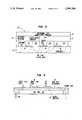
- FIG. 4is a cross-sectional schematic view of a multichip thin-film module.
- each interconnect signal planerequires approximately ten (1) separate steps. These steps can be briefly described as follows:
- the substrate 14, FIG. 2is a standard silicon wafer in the preferred embodiment. Due to the particular materials used in the preferred embodiment, it is desirable to provide a diffusion barrier for the metal used in Step 2, discussed below. Other materials can be used as the substrate such as alumina, silicon carbide or other kinds of ceramic can also be used.
- the substrategoes through a standard cleaning procedure typically used for silicon wafers. The cleaning procedure includes a ten-minute immersion in a boiling solution of ammonium hydroxide, hydrogen peroxide and water. This is followed by a ten-minute rinse in flowing deionized water. After the wafer is rinsed, it is then immersed for ten minutes in a boiling solution of sulfuric acid and hydrogen peroxide.
- the second immersionis then followed by a second ten-minute rinse in flowing deionized water and then the wafer is spun dried in a nitrogen environment. It should be noted that other cleaning procedures can be used.
- the major objects of the cleaning stepare to provide a wafer free of particles and organic contaminants.
- the cleaned wafersare then loaded into planetary fixtures.
- a planetary fixtureis a device in which a plurality of wafers may be subjected to rotation about an axis to ensure uniform metallization as discussed below.
- three planetary fixtures, each containing seven wafers,may be inserted in an evaporator at a time.
- the wafersare then patterned using standard photolithographic techniques to form a first pattern 16, FIG. 2, of thin-film metallic interconnect lines on the surface of the substrate.
- the thickness of the thin-film metallic interconnect linesis in the range of 500 to 5,000 Angstroms.
- the thickness of the thin-film metallic interconnect linesis approximately 1,000 Angstroms consisting of approximately 100 Angstroms of chromium overlaid by 900 Angstroms of gold. These thin-film are sufficiently thin that planarization is easily accomplished. It should be noted that in other embodiments, other materials ay be used to form the thin-film metallic pattern such as copper or silver.
- Another technique for providing the thin-film patternis the use of the "lift-off" technique.
- the waferis coated with a photoresist on which the thin-film pattern is defined.
- Metalis then evaporated onto the defined pattern and the photoresist is rinsed away, leaving the metal adhering in only the desired areas.
- a photosensitive polyimide precursor 18, FIG. 2is applied by spin coating on the patterned thin-film metallized substrate.
- other methods of applicationmay be used such as spraying, dipping and rolling.
- sprayingdipping and rolling.
- other materialsmay be used. These materials will be mentioned below and will not be discussed here since each particular material may require difference procedures than those discussed in the preferred embodiment.
- the product produced by Step 3is then prebaked at 70 degrees Centigrade for 180 mnutes to remove the solvent and partially harden the polyimide precursor.
- the prebake timeis dependent on the thickness of the polyimide precursor.
- the thickness of the polyimide precursoris typically 11 microns in the preferred embodiment.
- the polyimide precursoris next exposed using relatively standard photolithographic techniques. First a photomask containing a pattern of the thin-film metallic interconnect lines is aligned with the thin-film metallic interconnect lines on the substrate. In the preferred embodiment, it is possible to see the thin-film metallic interconnect lines through the dielectric in order to accomplish the alignment process. After alignment, the polyimide precursor is then exposed to ultraviolet light to render the exposed areas insoluble.
- the exposed polyimide photoresistis then subjected to a fairly standard spray development technique.
- Other techniquesmay be used to develop the photoresist such as dipping techniques.
- the spray techniquethe wafer is placed on a spinner and then the developer is sprayed onto the spinning wafer. This technique is repeated until a series of trenches 20, FIG. 2, are formed over the thin-film metallic interconnect lines.
- the deviceis then placed into a plasma etcher to remove any dielectric residue remaining in the trenches over the thin-film metallic interconnect lines.
- a plasma etcherto remove any dielectric residue remaining in the trenches over the thin-film metallic interconnect lines.
- an eight percent oxygen/argon plasmais used at a pressure of 3 torr for 2 minutes at a power of 100 watts.
- the wafersare then subjected to an intermediate bake procedure to partially cure the dielectric.
- thisentails heating the wafers to 200 degrees Centigrade for 90 minutes.
- the purpose of the next stepwhich is the electroplating step. If the dielectric layer is not sufficiently cured prior to the electroplating, the dielectric may peel off during the electroplating stage.
- One of the effects of the intermediate bakeis to partially transform the polyimide precursor into polyimide.
- the thin-film metallic interconnect patternis next subjected to an electroplating procedure.
- This procedureincludes placing each wafer in a fixture in which electrical connection can be made to the thin-film metallic pattern.
- the wafer and fixtureare then placed in an electroplating bath and a series of thicker metallic interconnect lines 22, FIG. 2, are formed over the thin-film metallic interconnect pattern.
- the final thickness of the dielectric layeris chosen so that it is approximately equal to the thickness of the electroplated conductors.
- the thickness of the electroplated conductorsis approximately 5 microns.
- the thicker metal inter connect linesmay be in the rang of 1 to 10 microns. It should also be noted that other techniques for forming the thicker metal interconnect lines may be used such as electroless plating.
- the product produced by Step 9is then subjected to a final bake to completely cure the polymer.
- the wafersare subjected to a post bake of 400 degrees Centigrade for 50 minutes in an inert atmosphere.
- the purpose of the post bakeis to fully convert the polyimide precursor to polyimide.
- One of the effects of the conversion of the precursor to polyimideis to cause the polymer to shrink in a predictable fashion.
- the polyimide dielectric layer and the thicker metal interconnect linesform a substantially planar surface.
- the process described abovemay be repeated to produce multilayered interconnect signal planes for connecting multiple integrated circuits as illustrated by device 24 in FIG. 3. It should be noted that before the procedures described above are repeated to produce each signal plane, an intermediate layer of dielectric 31 must be deposited for insulation purposes.
- the intermediate layercontains vias 26, FIG. 3, for electrical connection between selected interconnect lines.
- the interconnect lines 28 in the lower planeare in a direction generally orthogonal to the interconnect lines 30 in the upper plane.
- the intermediate dielectric layer and the metallic viasare produced in a fashion very similar to the production of the thicker metal interconnect lines. However, it is not necessary to produce a thin-film metallic base since the underlying metal conductors act as a base for the growth of metal in vias.
- a plurality of semiconductor integrated circuitsmay be electrically connected to the electrical interconnect planes of the subject invention.
- FIG. 4As can be seen in the figure, a silicon substrate 32 having thin-film multilayer interconnect signal planes 35 in accordance with the subject invention is electrically connected 34 to a plurality of semiconductor integrated circuits chips 36.
- a heat sink 38may be provided which is further described in U.S. patent application No. 698,472, entitled A NEW MULTICHIP THIN-FILM MODULE.
- this pathis typically formed along a perimeter of the substrate so that the path can be subsequently destroyed after the thicker metallic interconnect lines have been formed. In other embodiments, this path may be located in other portions on the substrate. In those embodiments in which electroless plating is used to form the thicker metallic interconnect lines, this path is not necessary.
- a convention polyimide precursormay be used instead of using a photosensitive polyimide precursor.
- a conventional polyimide precursoris used that is not photosensitive, different techniques must be used for creating patterns on the dielectric layer.
- Other techniquesinclude masking the polyimide with an inorganic layer such as silicon dioxide or aluminum. These inorganic layers are patterned with conventional photolithography and serve as an etching mask for the polyimide.
- the etching procedure for the polyimideentails exposing the polyimide and mask structure to oxygen, or other plasma, which then removes the exposed area which form the trenches discussed above.
- polymersmay be used instead of any form of polyimide.
- polymethylmethacrylate, or polytetrafluoroethyleneas the dielectric material.
- nonpolymeric materialsfor example, silicon dioxide or silicon nitride may be used as the dielectric. If a non-polymeric material is used as the dielectric, a polymeric etching mask is typically applied and the above-discussed trenches are etched by liquid echants or plasma etching methods.
- the subject inventionis advantageous in that the characteristic impedance can be controlled to be within 30 to 300 ohms because the subject invention provides for well-defined geometrics which are highly planar.
- the precise geometric configuration of the conductive interconnect lines and their relationship to the dielectric layerscan be well controlled to produce interconnect lines which are substantially rectangular as opposed to trapezoidal interconnect lines.
- the fact that the interconnect lines are substantially rectangular as opposed to trapezoidalis important, not so much from any specific shape requirements, but is important from the point of view that the specific dimensions (regardless of what dimensions or shape are chosen) are highly reproducible and uniform using the fabrication methods described here.
- the actual device produced in accordance with the methods described hereinis closer to theoretical geometrics than devices using prior-art techniques.
- the impedance of the devicedepends on the dielectric constant and its geometrical dimensions which can both be fabricated to high precision with the planarized electrical connection process discussed in this patent application.
- the planarized processis superior to other non-planar processes because firstly, all dimension of the device are better defined and secondly the planar process is inherently less susceptible to defects (either a short between the differential metal layers, or an open within a metal layer). It is a practical way to make multi-metal layer with thin dielectric insulator layers in between the metal layer.
Landscapes
- Engineering & Computer Science (AREA)
- Microelectronics & Electronic Packaging (AREA)
- Physics & Mathematics (AREA)
- Condensed Matter Physics & Semiconductors (AREA)
- General Physics & Mathematics (AREA)
- Computer Hardware Design (AREA)
- Power Engineering (AREA)
- Manufacturing & Machinery (AREA)
- Ceramic Engineering (AREA)
- Internal Circuitry In Semiconductor Integrated Circuit Devices (AREA)
Abstract
Description
Claims (7)
Priority Applications (1)
| Application Number | Priority Date | Filing Date | Title |
|---|---|---|---|
| US07/257,171US4996584A (en) | 1985-01-31 | 1988-10-13 | Thin-film electrical connections for integrated circuits |
Applications Claiming Priority (3)
| Application Number | Priority Date | Filing Date | Title |
|---|---|---|---|
| US06/697,092US4705606A (en) | 1985-01-31 | 1985-01-31 | Thin-film electrical connections for integrated circuits |
| US18065388A | 1988-04-11 | 1988-04-11 | |
| US07/257,171US4996584A (en) | 1985-01-31 | 1988-10-13 | Thin-film electrical connections for integrated circuits |
Related Parent Applications (1)
| Application Number | Title | Priority Date | Filing Date |
|---|---|---|---|
| US18065388AContinuation | 1985-01-31 | 1988-04-11 |
Publications (1)
| Publication Number | Publication Date |
|---|---|
| US4996584Atrue US4996584A (en) | 1991-02-26 |
Family
ID=27391314
Family Applications (1)
| Application Number | Title | Priority Date | Filing Date |
|---|---|---|---|
| US07/257,171Expired - LifetimeUS4996584A (en) | 1985-01-31 | 1988-10-13 | Thin-film electrical connections for integrated circuits |
Country Status (1)
| Country | Link |
|---|---|
| US (1) | US4996584A (en) |
Cited By (34)
| Publication number | Priority date | Publication date | Assignee | Title |
|---|---|---|---|---|
| US5243222A (en)* | 1991-04-05 | 1993-09-07 | International Business Machines Corporation | Copper alloy metallurgies for VLSI interconnection structures |
| US5247204A (en)* | 1990-06-05 | 1993-09-21 | Seiko Epson Corporation | Semiconductor device having multilayer interconnection structure |
| US5296742A (en)* | 1990-11-21 | 1994-03-22 | Nec Corporation | Multilayered integrated circuit chip wiring arrangement |
| US5442237A (en)* | 1991-10-21 | 1995-08-15 | Motorola Inc. | Semiconductor device having a low permittivity dielectric |
| US5880015A (en)* | 1991-04-30 | 1999-03-09 | Sgs-Thomson Microelectronics, Inc. | Method of producing stepped wall interconnects and gates |
| US5940729A (en)* | 1996-04-17 | 1999-08-17 | International Business Machines Corp. | Method of planarizing a curved substrate and resulting structure |
| US6002176A (en)* | 1996-10-11 | 1999-12-14 | Sharp Laboratories Of America, Inc. | Differential copper deposition on integrated circuit surfaces |
| US6020266A (en)* | 1997-12-31 | 2000-02-01 | Intel Corporation | Single step electroplating process for interconnect via fill and metal line patterning |
| US6107674A (en)* | 1993-05-05 | 2000-08-22 | Ixys Corporation | Isolated multi-chip devices |
| US6147408A (en)* | 1997-09-18 | 2000-11-14 | Ebara Corporation | Method of forming embedded copper interconnections and embedded copper interconnection structure |
| US6147393A (en)* | 1993-05-05 | 2000-11-14 | Ixys Corporation | Isolated multi-chip devices |
| US6169024B1 (en) | 1998-09-30 | 2001-01-02 | Intel Corporation | Process to manufacture continuous metal interconnects |
| US6171953B1 (en) | 1998-08-20 | 2001-01-09 | The United States Of America As Represented By The Secretary Of The Navy | Processes for making electronic devices with rubidum barrier film |
| US6208016B1 (en) | 1998-09-10 | 2001-03-27 | Micron Technology, Inc. | Forming submicron integrated-circuit wiring from gold, silver, copper and other metals |
| US6211073B1 (en) | 1998-02-27 | 2001-04-03 | Micron Technology, Inc. | Methods for making copper and other metal interconnections in integrated circuits |
| US6261941B1 (en)* | 1998-02-12 | 2001-07-17 | Georgia Tech Research Corp. | Method for manufacturing a multilayer wiring substrate |
| US6284656B1 (en) | 1998-08-04 | 2001-09-04 | Micron Technology, Inc. | Copper metallurgy in integrated circuits |
| US6326253B1 (en)* | 1998-07-08 | 2001-12-04 | Matsushita Electric Industrial Co., Ltd. | Method for fabricating semiconductor device including MIS and bipolar transistors |
| US6351036B1 (en)* | 1998-08-20 | 2002-02-26 | The United States Of America As Represented By The Secretary Of The Navy | Electronic devices with a barrier film and process for making same |
| US20020025675A1 (en)* | 2000-05-03 | 2002-02-28 | Chu Tak Kin | Electronic devices with diffusion barrier and process for making same |
| US6413854B1 (en) | 1999-08-24 | 2002-07-02 | International Business Machines Corp. | Method to build multi level structure |
| US20020098677A1 (en)* | 2000-05-31 | 2002-07-25 | Micron Technology, Inc. | Multilevel copper interconnects with low-k dielectrics and air gaps |
| US20020127845A1 (en)* | 1999-03-01 | 2002-09-12 | Paul A. Farrar | Conductive structures in integrated circuits |
| US20030146516A1 (en)* | 1999-01-22 | 2003-08-07 | Mitsubishi Denki Kabushiki Kaisha | Semiconductor device including a plurality of interconnection layers, manufacturing method thereof and method of designing semiconductor circuit used in the manufacturing method |
| US6743716B2 (en) | 2000-01-18 | 2004-06-01 | Micron Technology, Inc. | Structures and methods to enhance copper metallization |
| US6756298B2 (en) | 2000-01-18 | 2004-06-29 | Micron Technology, Inc. | Methods and apparatus for making integrated-circuit wiring from copper, silver, gold, and other metals |
| US20040169213A1 (en)* | 2000-01-18 | 2004-09-02 | Micron Technology, Inc. | Integrated circuit and seed layers |
| US20050023699A1 (en)* | 2000-01-18 | 2005-02-03 | Micron Technology, Inc. | Selective electroless-plated copper metallization |
| US20050032352A1 (en)* | 2003-08-05 | 2005-02-10 | Micron Technology, Inc. | H2 plasma treatment |
| US20050112871A1 (en)* | 2000-05-31 | 2005-05-26 | Micron Technology, Inc. | Multilevel copper interconnect with double passivation |
| US20050230262A1 (en)* | 2004-04-20 | 2005-10-20 | Semitool, Inc. | Electrochemical methods for the formation of protective features on metallized features |
| US20060024947A1 (en)* | 2002-07-29 | 2006-02-02 | Wolfgang Clements | Electronic component comprising predominantly organic functional materials and a method for the production thereof |
| US20060246733A1 (en)* | 2000-01-18 | 2006-11-02 | Micron Technology, Inc. | Method for making integrated circuits |
| US20120112364A1 (en)* | 2010-11-04 | 2012-05-10 | Samsung Electronics Co., Ltd. | Wiring structure of semiconductor device |
Citations (30)
| Publication number | Priority date | Publication date | Assignee | Title |
|---|---|---|---|---|
| US3189973A (en)* | 1961-11-27 | 1965-06-22 | Bell Telephone Labor Inc | Method of fabricating a semiconductor device |
| US3360349A (en)* | 1965-04-01 | 1967-12-26 | Sperry Rand Corp | Copper layer bonded to a non-conductive layer by means of a copper alloy |
| DE2015643A1 (en)* | 1969-04-02 | 1970-11-05 | International Business Machines Corp., Armonk, N.Y. (V.St.A.) | Process for the production of multilayer electrical circuit panels |
| US3729814A (en)* | 1967-04-04 | 1973-05-01 | Gen Electric | Method for making a composite |
| US3781596A (en)* | 1972-07-07 | 1973-12-25 | R Galli | Semiconductor chip carriers and strips thereof |
| US3791858A (en)* | 1971-12-13 | 1974-02-12 | Ibm | Method of forming multi-layer circuit panels |
| US3876460A (en)* | 1974-01-24 | 1975-04-08 | Plessey Inc | Fine-line thick-film substrate fabrication |
| US3981691A (en)* | 1974-07-01 | 1976-09-21 | Minnesota Mining And Manufacturing Company | Metal-clad dielectric sheeting having an improved bond between the metal and dielectric layers |
| US4021838A (en)* | 1974-11-20 | 1977-05-03 | International Business Machines Corporation | Semiconductor integrated circuit devices |
| US4074342A (en)* | 1974-12-20 | 1978-02-14 | International Business Machines Corporation | Electrical package for lsi devices and assembly process therefor |
| US4101402A (en)* | 1975-07-25 | 1978-07-18 | Rca Corporation | Adherence of metal films to polymeric materials |
| US4134125A (en)* | 1977-07-20 | 1979-01-09 | Bell Telephone Laboratories, Incorporated | Passivation of metallized semiconductor substrates |
| US4193849A (en)* | 1977-03-18 | 1980-03-18 | Nippon Mining Co., Ltd. | Method for making a raw board for use in printed circuits |
| DE2945385A1 (en)* | 1978-11-09 | 1980-05-14 | Maruman Integrated Circuits In | Multilayer substrate for semiconductor chip esp. integrated circuit - with conducting zones sepd. by insulating layers |
| US4210885A (en)* | 1978-06-30 | 1980-07-01 | International Business Machines Corporation | Thin film lossy line for preventing reflections in microcircuit chip package interconnections |
| US4221047A (en)* | 1979-03-23 | 1980-09-09 | International Business Machines Corporation | Multilayered glass-ceramic substrate for mounting of semiconductor device |
| US4231848A (en)* | 1978-05-08 | 1980-11-04 | Nippon Mining Co., Ltd. | Method for making a raw board for use in printed circuits |
| US4254445A (en)* | 1979-05-07 | 1981-03-03 | International Business Machines Corporation | Discretionary fly wire chip interconnection |
| JPS5718356A (en)* | 1980-07-07 | 1982-01-30 | Mitsubishi Electric Corp | Semiconductor memory storage |
| EP0046525A2 (en)* | 1980-08-18 | 1982-03-03 | International Business Machines Corporation | Planar multi-level metal-insulator structure comprising a substrate, a conductive interconnection pattern and a superposed conductive structure and a method to form such a structure |
| US4328530A (en)* | 1980-06-30 | 1982-05-04 | International Business Machines Corporation | Multiple layer, ceramic carrier for high switching speed VLSI chips |
| JPS57145997A (en)* | 1981-03-03 | 1982-09-09 | Matsushita Electric Ind Co Ltd | Formation of metallic film on film |
| US4349862A (en)* | 1980-08-11 | 1982-09-14 | International Business Machines Corporation | Capacitive chip carrier and multilayer ceramic capacitors |
| EP0060682A2 (en)* | 1981-03-12 | 1982-09-22 | Honeywell Inc. | Process for making dielectric stencilled microcircuits |
| EP0083020A2 (en)* | 1981-12-24 | 1983-07-06 | International Business Machines Corporation | Process for making multilayer integrated circuit substrate |
| US4395313A (en)* | 1982-07-29 | 1983-07-26 | General Motors Corporation | Vacuum pretreatment process for durable electroplated coatings on ABS and PPO plastics |
| US4430690A (en)* | 1982-10-07 | 1984-02-07 | International Business Machines Corporation | Low inductance MLC capacitor with metal impregnation and solder bar contact |
| US4566940A (en)* | 1981-04-21 | 1986-01-28 | Nippon Telegraph And Telephone Public Corporation | Manufacturing process for semiconductor integrated circuits |
| US4568413A (en)* | 1983-07-25 | 1986-02-04 | James J. Toth | Metallized and plated laminates |
| US4617193A (en)* | 1983-06-16 | 1986-10-14 | Digital Equipment Corporation | Planar interconnect for integrated circuits |
- 1988
- 1988-10-13USUS07/257,171patent/US4996584A/ennot_activeExpired - Lifetime
Patent Citations (31)
| Publication number | Priority date | Publication date | Assignee | Title |
|---|---|---|---|---|
| US3189973A (en)* | 1961-11-27 | 1965-06-22 | Bell Telephone Labor Inc | Method of fabricating a semiconductor device |
| US3360349A (en)* | 1965-04-01 | 1967-12-26 | Sperry Rand Corp | Copper layer bonded to a non-conductive layer by means of a copper alloy |
| US3729814A (en)* | 1967-04-04 | 1973-05-01 | Gen Electric | Method for making a composite |
| DE2015643A1 (en)* | 1969-04-02 | 1970-11-05 | International Business Machines Corp., Armonk, N.Y. (V.St.A.) | Process for the production of multilayer electrical circuit panels |
| US3791858A (en)* | 1971-12-13 | 1974-02-12 | Ibm | Method of forming multi-layer circuit panels |
| US3781596A (en)* | 1972-07-07 | 1973-12-25 | R Galli | Semiconductor chip carriers and strips thereof |
| US3876460A (en)* | 1974-01-24 | 1975-04-08 | Plessey Inc | Fine-line thick-film substrate fabrication |
| US3981691A (en)* | 1974-07-01 | 1976-09-21 | Minnesota Mining And Manufacturing Company | Metal-clad dielectric sheeting having an improved bond between the metal and dielectric layers |
| US4021838A (en)* | 1974-11-20 | 1977-05-03 | International Business Machines Corporation | Semiconductor integrated circuit devices |
| US4074342A (en)* | 1974-12-20 | 1978-02-14 | International Business Machines Corporation | Electrical package for lsi devices and assembly process therefor |
| US4101402A (en)* | 1975-07-25 | 1978-07-18 | Rca Corporation | Adherence of metal films to polymeric materials |
| US4193849A (en)* | 1977-03-18 | 1980-03-18 | Nippon Mining Co., Ltd. | Method for making a raw board for use in printed circuits |
| US4134125A (en)* | 1977-07-20 | 1979-01-09 | Bell Telephone Laboratories, Incorporated | Passivation of metallized semiconductor substrates |
| US4231848A (en)* | 1978-05-08 | 1980-11-04 | Nippon Mining Co., Ltd. | Method for making a raw board for use in printed circuits |
| US4210885A (en)* | 1978-06-30 | 1980-07-01 | International Business Machines Corporation | Thin film lossy line for preventing reflections in microcircuit chip package interconnections |
| DE2945385A1 (en)* | 1978-11-09 | 1980-05-14 | Maruman Integrated Circuits In | Multilayer substrate for semiconductor chip esp. integrated circuit - with conducting zones sepd. by insulating layers |
| EP0016306A1 (en)* | 1979-03-23 | 1980-10-01 | International Business Machines Corporation | Method of manufacturing a multi-layered glass-ceramic package for the mounting of semiconductor devices |
| US4221047A (en)* | 1979-03-23 | 1980-09-09 | International Business Machines Corporation | Multilayered glass-ceramic substrate for mounting of semiconductor device |
| US4254445A (en)* | 1979-05-07 | 1981-03-03 | International Business Machines Corporation | Discretionary fly wire chip interconnection |
| US4328530A (en)* | 1980-06-30 | 1982-05-04 | International Business Machines Corporation | Multiple layer, ceramic carrier for high switching speed VLSI chips |
| JPS5718356A (en)* | 1980-07-07 | 1982-01-30 | Mitsubishi Electric Corp | Semiconductor memory storage |
| US4349862A (en)* | 1980-08-11 | 1982-09-14 | International Business Machines Corporation | Capacitive chip carrier and multilayer ceramic capacitors |
| EP0046525A2 (en)* | 1980-08-18 | 1982-03-03 | International Business Machines Corporation | Planar multi-level metal-insulator structure comprising a substrate, a conductive interconnection pattern and a superposed conductive structure and a method to form such a structure |
| JPS57145997A (en)* | 1981-03-03 | 1982-09-09 | Matsushita Electric Ind Co Ltd | Formation of metallic film on film |
| EP0060682A2 (en)* | 1981-03-12 | 1982-09-22 | Honeywell Inc. | Process for making dielectric stencilled microcircuits |
| US4566940A (en)* | 1981-04-21 | 1986-01-28 | Nippon Telegraph And Telephone Public Corporation | Manufacturing process for semiconductor integrated circuits |
| EP0083020A2 (en)* | 1981-12-24 | 1983-07-06 | International Business Machines Corporation | Process for making multilayer integrated circuit substrate |
| US4395313A (en)* | 1982-07-29 | 1983-07-26 | General Motors Corporation | Vacuum pretreatment process for durable electroplated coatings on ABS and PPO plastics |
| US4430690A (en)* | 1982-10-07 | 1984-02-07 | International Business Machines Corporation | Low inductance MLC capacitor with metal impregnation and solder bar contact |
| US4617193A (en)* | 1983-06-16 | 1986-10-14 | Digital Equipment Corporation | Planar interconnect for integrated circuits |
| US4568413A (en)* | 1983-07-25 | 1986-02-04 | James J. Toth | Metallized and plated laminates |
Non-Patent Citations (27)
| Title |
|---|
| "A Planar Metallization Process--Its Application to Tri-Level Aluminum Interconnection", by Moriya, et al. dated 1983, pp. 550-553. |
| "Electrical Design of a High Speed Computer Packaging System", by Evan E. Davidson dated Sep., 1983, pp. 272-282. |
| "High-Density High-Impedance Hybrid Circuit Technology for Gigahertz Logic", by Edward T. Lewis dated Dec. 1979, pp. 441-450. |
| "High-Density Multilayer Interconnection with Photo-Sensitive Polyimide Dielectric and Electroplating Conductor", by Moriya et al. dated 1984, pp. 82-87. |
| "Silicon-on-Silicon Packaging", by Spielberger, et al. dated Jun. 1984, pp. 193-196. |
| "The Thin-Film Module as a High Performance Semiconductor Package", IBM J. Res. Develop., vol. 26, No. 3, May 1982. |
| A Planar Metallization Process Its Application to Tri Level Aluminum Interconnection , by Moriya, et al. dated 1983, pp. 550 553.* |
| C. W. Ho et al., The Thin Film Module as a High Performance Semiconductor Package, IBM J. Res. Develop., vol. 26, No. 3, May, 1982.* |
| C. W. Ho et al., The Thin-Film Module as a High-Performance Semiconductor Package, IBM J. Res. Develop., vol. 26, No. 3, May, 1982. |
| Davidson, "Electrical Design of High Speed Computer Packaging System," (Sep. 1983), IEEE Trans. on Components Hybrids & Mftr. Tech., CHMT-6, #3, pp. 272-282. |
| Davidson, Electrical Design of High Speed Computer Packaging System, (Sep. 1983), IEEE Trans. on Components Hybrids & Mftr. Tech., CHMT 6, 3, pp. 272 282.* |
| Electrical Design of a High Speed Computer Packaging System , by Evan E. Davidson dated Sep., 1983, pp. 272 282.* |
| European Search Report for Application No. EP 85 30 8479 Completed 10 22 86; pp. 1 3.* |
| European Search Report for Application No. EP 85 30 8479 Completed 10-22-86; pp. 1-3. |
| High Density High Impedance Hybrid Circuit Technology for Gigahertz Logic , by Edward T. Lewis dated Dec. 1979, pp. 441 450.* |
| High Density Multilayer Interconnection with Photo Sensitive Polyimide Dielectric and Electroplating Conductor , by Moriya et al. dated 1984, pp. 82 87.* |
| IBM Technical Disclosure Bulletin, vol. 13, No. 6, Nov. 1970, Planar Process by S. A. Abbas et al.* |
| Lewis, "High Density High Impedance Hybrid Circuit Tech., Etc.," (Dec. 1979), IEEE Trans. on Components, Hybrids & Mftr. Tech., CHMT-2, #4, pp. 441-450. |
| Lewis, High Density High Impedance Hybrid Circuit Tech., Etc., (Dec. 1979), IEEE Trans. on Components, Hybrids & Mftr. Tech., CHMT 2, 4, pp. 441 450.* |
| Moriya et al., "A Planar Metallization Process, Etc.", (1983), International Electron Devices Mtg., IEEE, pp. 550-552. |
| Moriya et al., "High Density Multilayer Interconnection, Etc.", (1984), 1984 Proceedings of 34th Elec. Components Conf., pp. 82-87. |
| Moriya et al., A Planar Metallization Process, Etc. , (1983), International Electron Devices Mtg., IEEE, pp. 550 552.* |
| Moriya et al., High Density Multilayer Interconnection, Etc. , (1984), 1984 Proceedings of 34th Elec. Components Conf., pp. 82 87.* |
| Silicon on Silicon Packaging , by Spielberger, et al. dated Jun. 1984, pp. 193 196.* |
| Spielberger et al., "Silicon-on-Silicon Packaging", (Jun. 1984), IEEE Transactions on Components, Hybrids & Mftr. Tech., CHMT-7, No. 7, pp. 193-196. |
| Spielberger et al., Silicon on Silicon Packaging , (Jun. 1984), IEEE Transactions on Components, Hybrids & Mftr. Tech., CHMT 7, No. 7, pp. 193 196.* |
| The Thin Film Module as a High Performance Semiconductor Package , IBM J. Res. Develop., vol. 26, No. 3, May 1982.* |
Cited By (75)
| Publication number | Priority date | Publication date | Assignee | Title |
|---|---|---|---|---|
| US5247204A (en)* | 1990-06-05 | 1993-09-21 | Seiko Epson Corporation | Semiconductor device having multilayer interconnection structure |
| US5296742A (en)* | 1990-11-21 | 1994-03-22 | Nec Corporation | Multilayered integrated circuit chip wiring arrangement |
| US5243222A (en)* | 1991-04-05 | 1993-09-07 | International Business Machines Corporation | Copper alloy metallurgies for VLSI interconnection structures |
| US5880015A (en)* | 1991-04-30 | 1999-03-09 | Sgs-Thomson Microelectronics, Inc. | Method of producing stepped wall interconnects and gates |
| US5442237A (en)* | 1991-10-21 | 1995-08-15 | Motorola Inc. | Semiconductor device having a low permittivity dielectric |
| US6107674A (en)* | 1993-05-05 | 2000-08-22 | Ixys Corporation | Isolated multi-chip devices |
| US6147393A (en)* | 1993-05-05 | 2000-11-14 | Ixys Corporation | Isolated multi-chip devices |
| US5940729A (en)* | 1996-04-17 | 1999-08-17 | International Business Machines Corp. | Method of planarizing a curved substrate and resulting structure |
| US6150255A (en)* | 1996-04-17 | 2000-11-21 | International Business Machines Corporation | Method of planarizing a curved substrate and resulting structure |
| US6002176A (en)* | 1996-10-11 | 1999-12-14 | Sharp Laboratories Of America, Inc. | Differential copper deposition on integrated circuit surfaces |
| US6147408A (en)* | 1997-09-18 | 2000-11-14 | Ebara Corporation | Method of forming embedded copper interconnections and embedded copper interconnection structure |
| US6020266A (en)* | 1997-12-31 | 2000-02-01 | Intel Corporation | Single step electroplating process for interconnect via fill and metal line patterning |
| US6384481B1 (en) | 1997-12-31 | 2002-05-07 | Intel Corporation | Single step electroplating process for interconnect via fill and metal line patterning |
| US6261941B1 (en)* | 1998-02-12 | 2001-07-17 | Georgia Tech Research Corp. | Method for manufacturing a multilayer wiring substrate |
| US6211073B1 (en) | 1998-02-27 | 2001-04-03 | Micron Technology, Inc. | Methods for making copper and other metal interconnections in integrated circuits |
| US6984891B2 (en) | 1998-02-27 | 2006-01-10 | Micron Technology, Inc. | Methods for making copper and other metal interconnections in integrated circuits |
| US6326253B1 (en)* | 1998-07-08 | 2001-12-04 | Matsushita Electric Industrial Co., Ltd. | Method for fabricating semiconductor device including MIS and bipolar transistors |
| US6614099B2 (en) | 1998-08-04 | 2003-09-02 | Micron Technology, Inc. | Copper metallurgy in integrated circuits |
| US6284656B1 (en) | 1998-08-04 | 2001-09-04 | Micron Technology, Inc. | Copper metallurgy in integrated circuits |
| US6188134B1 (en)* | 1998-08-20 | 2001-02-13 | The United States Of America As Represented By The Secretary Of The Navy | Electronic devices with rubidium barrier film and process for making same |
| US6171953B1 (en) | 1998-08-20 | 2001-01-09 | The United States Of America As Represented By The Secretary Of The Navy | Processes for making electronic devices with rubidum barrier film |
| US6351036B1 (en)* | 1998-08-20 | 2002-02-26 | The United States Of America As Represented By The Secretary Of The Navy | Electronic devices with a barrier film and process for making same |
| US6211049B1 (en) | 1998-09-10 | 2001-04-03 | Micron Technology, Inc. | Forming submicron integrated-circuit wiring from gold, silver, copper, and other metals |
| US6288442B1 (en)* | 1998-09-10 | 2001-09-11 | Micron Technology, Inc. | Integrated circuit with oxidation-resistant polymeric layer |
| US20010010403A1 (en)* | 1998-09-10 | 2001-08-02 | Micron Technology, Inc. | Forming submicron integrated-circuit wiring from gold, silver, copper, and other metals |
| US6208016B1 (en) | 1998-09-10 | 2001-03-27 | Micron Technology, Inc. | Forming submicron integrated-circuit wiring from gold, silver, copper and other metals |
| US6552432B2 (en) | 1998-09-10 | 2003-04-22 | Micron Technology, Inc. | Mask on a polymer having an opening width less than that of the opening in the polymer |
| US6849927B2 (en) | 1998-09-10 | 2005-02-01 | Micron Technology, Inc. | Forming submicron integrated-circuit wiring from gold, silver, copper, and other metals |
| US7166922B1 (en) | 1998-09-30 | 2007-01-23 | Intel Corporation | Continuous metal interconnects |
| US6169024B1 (en) | 1998-09-30 | 2001-01-02 | Intel Corporation | Process to manufacture continuous metal interconnects |
| US20030146516A1 (en)* | 1999-01-22 | 2003-08-07 | Mitsubishi Denki Kabushiki Kaisha | Semiconductor device including a plurality of interconnection layers, manufacturing method thereof and method of designing semiconductor circuit used in the manufacturing method |
| US6835647B2 (en)* | 1999-01-22 | 2004-12-28 | Renesas Technology Corp. | Semiconductor device including a plurality of interconnection layers, manufacturing method thereof and method of designing semiconductor circuit used in the manufacturing method |
| US20020127845A1 (en)* | 1999-03-01 | 2002-09-12 | Paul A. Farrar | Conductive structures in integrated circuits |
| US20050285272A1 (en)* | 1999-03-01 | 2005-12-29 | Micron Technology, Inc. | Conductive structures in integrated circuits |
| US6413854B1 (en) | 1999-08-24 | 2002-07-02 | International Business Machines Corp. | Method to build multi level structure |
| US20040206308A1 (en)* | 2000-01-18 | 2004-10-21 | Micron Technologies, Inc. | Methods and apparatus for making integrated-circuit wiring from copper, silver, gold, and other metals |
| US7368378B2 (en) | 2000-01-18 | 2008-05-06 | Micron Technology, Inc. | Methods for making integrated-circuit wiring from copper, silver, gold, and other metals |
| US20040217481A1 (en)* | 2000-01-18 | 2004-11-04 | Micron Technology, Inc. | Structures and methods to enhance copper metallization |
| US8779596B2 (en) | 2000-01-18 | 2014-07-15 | Micron Technology, Inc. | Structures and methods to enhance copper metallization |
| US6756298B2 (en) | 2000-01-18 | 2004-06-29 | Micron Technology, Inc. | Methods and apparatus for making integrated-circuit wiring from copper, silver, gold, and other metals |
| US20050023699A1 (en)* | 2000-01-18 | 2005-02-03 | Micron Technology, Inc. | Selective electroless-plated copper metallization |
| US7745934B2 (en) | 2000-01-18 | 2010-06-29 | Micron Technology, Inc. | Integrated circuit and seed layers |
| US7670469B2 (en) | 2000-01-18 | 2010-03-02 | Micron Technology, Inc. | Methods and apparatus for making integrated-circuit wiring from copper, silver, gold, and other metals |
| US20090243106A1 (en)* | 2000-01-18 | 2009-10-01 | Farrar Paul A | Structures and methods to enhance copper metallization |
| US7535103B2 (en) | 2000-01-18 | 2009-05-19 | Micron Technology, Inc. | Structures and methods to enhance copper metallization |
| US6743716B2 (en) | 2000-01-18 | 2004-06-01 | Micron Technology, Inc. | Structures and methods to enhance copper metallization |
| US20090001586A1 (en)* | 2000-01-18 | 2009-01-01 | Micron Technology, Inc. | Integrated circuit and seed layers |
| US7402516B2 (en) | 2000-01-18 | 2008-07-22 | Micron Technology, Inc. | Method for making integrated circuits |
| US7394157B2 (en) | 2000-01-18 | 2008-07-01 | Micron Technology, Inc. | Integrated circuit and seed layers |
| US7378737B2 (en) | 2000-01-18 | 2008-05-27 | Micron Technology, Inc. | Structures and methods to enhance copper metallization |
| US20040169213A1 (en)* | 2000-01-18 | 2004-09-02 | Micron Technology, Inc. | Integrated circuit and seed layers |
| US7105914B2 (en) | 2000-01-18 | 2006-09-12 | Micron Technology, Inc. | Integrated circuit and seed layers |
| US20060246733A1 (en)* | 2000-01-18 | 2006-11-02 | Micron Technology, Inc. | Method for making integrated circuits |
| US20060255462A1 (en)* | 2000-01-18 | 2006-11-16 | Micron Technology, Inc. | Structures and methods to enhance copper metallization |
| US7301190B2 (en) | 2000-01-18 | 2007-11-27 | Micron Technology, Inc. | Structures and methods to enhance copper metallization |
| US20070085213A1 (en)* | 2000-01-18 | 2007-04-19 | Micron Technology, Inc. | Selective electroless-plated copper metallization |
| US7285196B2 (en) | 2000-01-18 | 2007-10-23 | Micron Technology, Inc. | Methods and apparatus for making integrated-circuit wiring from copper, silver, gold, and other metals |
| US20070141830A1 (en)* | 2000-01-18 | 2007-06-21 | Micron Technology, Inc. | Methods for making integrated-circuit wiring from copper, silver, gold, and other metals |
| US7253521B2 (en) | 2000-01-18 | 2007-08-07 | Micron Technology, Inc. | Methods for making integrated-circuit wiring from copper, silver, gold, and other metals |
| US7262505B2 (en) | 2000-01-18 | 2007-08-28 | Micron Technology, Inc. | Selective electroless-plated copper metallization |
| US7262130B1 (en) | 2000-01-18 | 2007-08-28 | Micron Technology, Inc. | Methods for making integrated-circuit wiring from copper, silver, gold, and other metals |
| US6881669B2 (en) | 2000-05-03 | 2005-04-19 | The United States Of America As Represented By The Secretary Of The Navy | Process for making electronic devices having a monolayer diffusion barrier |
| US20020025675A1 (en)* | 2000-05-03 | 2002-02-28 | Chu Tak Kin | Electronic devices with diffusion barrier and process for making same |
| US20020098677A1 (en)* | 2000-05-31 | 2002-07-25 | Micron Technology, Inc. | Multilevel copper interconnects with low-k dielectrics and air gaps |
| US7067421B2 (en) | 2000-05-31 | 2006-06-27 | Micron Technology, Inc. | Multilevel copper interconnect with double passivation |
| US6995470B2 (en) | 2000-05-31 | 2006-02-07 | Micron Technology, Inc. | Multilevel copper interconnects with low-k dielectrics and air gaps |
| US20050112871A1 (en)* | 2000-05-31 | 2005-05-26 | Micron Technology, Inc. | Multilevel copper interconnect with double passivation |
| US7091611B2 (en) | 2000-05-31 | 2006-08-15 | Micron Technology, Inc. | Multilevel copper interconnects with low-k dielectrics and air gaps |
| US20040164419A1 (en)* | 2000-05-31 | 2004-08-26 | Micron Technology, Inc. | Multilevel copper interconnects with low-k dielectrics and air gaps |
| US20060024947A1 (en)* | 2002-07-29 | 2006-02-02 | Wolfgang Clements | Electronic component comprising predominantly organic functional materials and a method for the production thereof |
| US7220665B2 (en) | 2003-08-05 | 2007-05-22 | Micron Technology, Inc. | H2 plasma treatment |
| US7504674B2 (en) | 2003-08-05 | 2009-03-17 | Micron Technology, Inc. | Electronic apparatus having a core conductive structure within an insulating layer |
| US20050032352A1 (en)* | 2003-08-05 | 2005-02-10 | Micron Technology, Inc. | H2 plasma treatment |
| US20050230262A1 (en)* | 2004-04-20 | 2005-10-20 | Semitool, Inc. | Electrochemical methods for the formation of protective features on metallized features |
| US20120112364A1 (en)* | 2010-11-04 | 2012-05-10 | Samsung Electronics Co., Ltd. | Wiring structure of semiconductor device |
Similar Documents
| Publication | Publication Date | Title |
|---|---|---|
| US4996584A (en) | Thin-film electrical connections for integrated circuits | |
| US4705606A (en) | Thin-film electrical connections for integrated circuits | |
| Jensen et al. | Copper/polyimide materials system for high performance packaging | |
| EP0099544B1 (en) | Method for forming conductive lines and via studs on lsi carrier substrates | |
| US4770897A (en) | Multilayer interconnection system for multichip high performance semiconductor packaging | |
| US5106461A (en) | High-density, multi-level interconnects, flex circuits, and tape for tab | |
| US4980034A (en) | High-density, multi-level interconnects, flex circuits, and tape for TAB | |
| US4920639A (en) | Method of making a multilevel electrical airbridge interconnect | |
| US4918811A (en) | Multichip integrated circuit packaging method | |
| EP0411165B1 (en) | Method of forming of an integrated circuit chip packaging structure | |
| KR960013632B1 (en) | Multichip integrated circuit package configuration and method | |
| US5436504A (en) | Interconnect structures having tantalum/tantalum oxide layers | |
| US4367119A (en) | Planar multi-level metal process with built-in etch stop | |
| US5112448A (en) | Self-aligned process for fabrication of interconnect structures in semiconductor applications | |
| EP0450381B1 (en) | Multilayer interconnection structure | |
| CN114188300B (en) | A thin-film and thick-film hybrid integrated ceramic substrate and preparation method thereof | |
| US4447824A (en) | Planar multi-level metal process with built-in etch stop | |
| US6576542B2 (en) | Conductive lines, coaxial lines, integrated circuitry, and methods of forming conductive lines, coaxial lines, and integrated circuitry | |
| US4520554A (en) | Method of making a multi-level metallization structure for semiconductor device | |
| US5661341A (en) | Method of manufacturing a composite structure for use in electronic devices and structure, manufactured by said method | |
| McDonald et al. | Multilevel interconnections for wafer scale integration | |
| JPH04290249A (en) | Manufacture of semiconductor device | |
| JP3272945B2 (en) | Manufacturing method of wiring board | |
| CN112687616B (en) | Preparation method of radio frequency tube case and radio frequency tube case | |
| Ray et al. | Dual-level metal (DLM) method for fabricating thin film wiring structures |
Legal Events
| Date | Code | Title | Description |
|---|---|---|---|
| STCF | Information on status: patent grant | Free format text:PATENTED CASE | |
| AS | Assignment | Owner name:AMERICAN MICROSYSTEMS, INC., IDAHO Free format text:ASSIGNMENT OF ASSIGNORS INTEREST.;ASSIGNOR:GOULD INC.;REEL/FRAME:006404/0707 Effective date:19921215 | |
| FEPP | Fee payment procedure | Free format text:PAYOR NUMBER ASSIGNED (ORIGINAL EVENT CODE: ASPN); ENTITY STATUS OF PATENT OWNER: LARGE ENTITY | |
| FPAY | Fee payment | Year of fee payment:4 | |
| FPAY | Fee payment | Year of fee payment:8 | |
| AS | Assignment | Owner name:AMERICAN MICROSYSTEMS HOLDING CORPORATION, IDAHO Free format text:MERGER;ASSIGNOR:AMERICAN MICROSYSTEMS, INC.;REEL/FRAME:011277/0491 Effective date:19970725 Owner name:GA-TEK INC., OHIO Free format text:MERGER AND CHANGE OF NAME;ASSIGNOR:AMERICAN MICROSYSTEMS HOLDING CORPORATION;REEL/FRAME:011277/0509 Effective date:19980101 | |
| AS | Assignment | Owner name:AMI SPINCO, INC., IDAHO Free format text:ASSIGNMENT OF ASSIGNORS INTEREST;ASSIGNOR:GA-TEK, INC.;REEL/FRAME:011369/0264 Effective date:20000729 | |
| AS | Assignment | Owner name:CREDIT SUISSE FIRST BOSTON, AS COLLATERAL AGENT, N Free format text:SECURITY INTEREST;ASSIGNOR:AMI SPINCO, INC.;REEL/FRAME:011457/0562 Effective date:20001221 | |
| AS | Assignment | Owner name:AMI SEMICONDUCTOR, INC., IDAHO Free format text:MERGER/CHANGE OF NAME;ASSIGNOR:AMI SPINCO, INC.;REEL/FRAME:011601/0413 Effective date:20001221 | |
| FPAY | Fee payment | Year of fee payment:12 | |
| REMI | Maintenance fee reminder mailed | ||
| AS | Assignment | Owner name:CREDIT SUISSE (F/K/A CREDIT SUISEE FIRST BOSTON), Free format text:SECURITY INTEREST;ASSIGNOR:AMI SEMICONDUCTOR, INC.;REEL/FRAME:016290/0206 Effective date:20050401 | |
| AS | Assignment | Owner name:AMI SEMICONDUCTOR, INC., IDAHO Free format text:PATENT RELEASE;ASSIGNOR:CREDIT SUISSE;REEL/FRAME:020679/0505 Effective date:20080317 Owner name:AMI SEMICONDUCTOR, INC.,IDAHO Free format text:PATENT RELEASE;ASSIGNOR:CREDIT SUISSE;REEL/FRAME:020679/0505 Effective date:20080317 | |
| AS | Assignment | Owner name:JPMORGAN CHASE BANK, N.A., NEW YORK Free format text:SECURITY AGREEMENT;ASSIGNORS:SEMICONDUCTOR COMPONENTS INDUSTRIES, LLC;AMIS HOLDINGS, INC.;AMI SEMICONDUCTOR, INC.;AND OTHERS;REEL/FRAME:021138/0070 Effective date:20080325 Owner name:JPMORGAN CHASE BANK, N.A.,NEW YORK Free format text:SECURITY AGREEMENT;ASSIGNORS:SEMICONDUCTOR COMPONENTS INDUSTRIES, LLC;AMIS HOLDINGS, INC.;AMI SEMICONDUCTOR, INC.;AND OTHERS;REEL/FRAME:021138/0070 Effective date:20080325 | |
| AS | Assignment | Owner name:AMI SPINCO, INC., IDAHO Free format text:RELEASE BY SECURED PARTY;ASSIGNOR:CREDIT SUISSE AG, CAYMAN ISLANDS BRANCH (F/K/A CREDIT SUISSE FIRST BOSTON);REEL/FRAME:038355/0131 Effective date:20160401 Owner name:AMI SEMICONDUCTOR, INC., IDAHO Free format text:RELEASE BY SECURED PARTY;ASSIGNOR:CREDIT SUISSE AG, CAYMAN ISLANDS BRANCH (F/K/A CREDIT SUISSE FIRST BOSTON);REEL/FRAME:038355/0131 Effective date:20160401 |