US4996583A - Stack type semiconductor package - Google Patents
Stack type semiconductor packageDownload PDFInfo
- Publication number
- US4996583A US4996583AUS07/477,542US47754290AUS4996583AUS 4996583 AUS4996583 AUS 4996583AUS 47754290 AUS47754290 AUS 47754290AUS 4996583 AUS4996583 AUS 4996583A
- Authority
- US
- United States
- Prior art keywords
- leads
- stacked
- plural
- chips
- chip
- Prior art date
- Legal status (The legal status is an assumption and is not a legal conclusion. Google has not performed a legal analysis and makes no representation as to the accuracy of the status listed.)
- Expired - Lifetime
Links
Images


Classifications
- H—ELECTRICITY
- H01—ELECTRIC ELEMENTS
- H01L—SEMICONDUCTOR DEVICES NOT COVERED BY CLASS H10
- H01L25/00—Assemblies consisting of a plurality of semiconductor or other solid state devices
- H01L25/03—Assemblies consisting of a plurality of semiconductor or other solid state devices all the devices being of a type provided for in a single subclass of subclasses H10B, H10D, H10F, H10H, H10K or H10N, e.g. assemblies of rectifier diodes
- H01L25/04—Assemblies consisting of a plurality of semiconductor or other solid state devices all the devices being of a type provided for in a single subclass of subclasses H10B, H10D, H10F, H10H, H10K or H10N, e.g. assemblies of rectifier diodes the devices not having separate containers
- H01L25/065—Assemblies consisting of a plurality of semiconductor or other solid state devices all the devices being of a type provided for in a single subclass of subclasses H10B, H10D, H10F, H10H, H10K or H10N, e.g. assemblies of rectifier diodes the devices not having separate containers the devices being of a type provided for in group H10D89/00
- H01L25/0657—Stacked arrangements of devices
- H—ELECTRICITY
- H01—ELECTRIC ELEMENTS
- H01L—SEMICONDUCTOR DEVICES NOT COVERED BY CLASS H10
- H01L23/00—Details of semiconductor or other solid state devices
- H01L23/48—Arrangements for conducting electric current to or from the solid state body in operation, e.g. leads, terminal arrangements ; Selection of materials therefor
- H01L23/488—Arrangements for conducting electric current to or from the solid state body in operation, e.g. leads, terminal arrangements ; Selection of materials therefor consisting of soldered or bonded constructions
- H01L23/495—Lead-frames or other flat leads
- H01L23/49572—Lead-frames or other flat leads consisting of thin flexible metallic tape with or without a film carrier
- H—ELECTRICITY
- H01—ELECTRIC ELEMENTS
- H01L—SEMICONDUCTOR DEVICES NOT COVERED BY CLASS H10
- H01L2225/00—Details relating to assemblies covered by the group H01L25/00 but not provided for in its subgroups
- H01L2225/03—All the devices being of a type provided for in the same main group of the same subclass of class H10, e.g. assemblies of rectifier diodes
- H01L2225/04—All the devices being of a type provided for in the same main group of the same subclass of class H10, e.g. assemblies of rectifier diodes the devices not having separate containers
- H01L2225/065—All the devices being of a type provided for in the same main group of the same subclass of class H10
- H01L2225/06503—Stacked arrangements of devices
- H01L2225/06527—Special adaptation of electrical connections, e.g. rewiring, engineering changes, pressure contacts, layout
- H—ELECTRICITY
- H01—ELECTRIC ELEMENTS
- H01L—SEMICONDUCTOR DEVICES NOT COVERED BY CLASS H10
- H01L2225/00—Details relating to assemblies covered by the group H01L25/00 but not provided for in its subgroups
- H01L2225/03—All the devices being of a type provided for in the same main group of the same subclass of class H10, e.g. assemblies of rectifier diodes
- H01L2225/04—All the devices being of a type provided for in the same main group of the same subclass of class H10, e.g. assemblies of rectifier diodes the devices not having separate containers
- H01L2225/065—All the devices being of a type provided for in the same main group of the same subclass of class H10
- H01L2225/06503—Stacked arrangements of devices
- H01L2225/06555—Geometry of the stack, e.g. form of the devices, geometry to facilitate stacking
- H—ELECTRICITY
- H01—ELECTRIC ELEMENTS
- H01L—SEMICONDUCTOR DEVICES NOT COVERED BY CLASS H10
- H01L2225/00—Details relating to assemblies covered by the group H01L25/00 but not provided for in its subgroups
- H01L2225/03—All the devices being of a type provided for in the same main group of the same subclass of class H10, e.g. assemblies of rectifier diodes
- H01L2225/04—All the devices being of a type provided for in the same main group of the same subclass of class H10, e.g. assemblies of rectifier diodes the devices not having separate containers
- H01L2225/065—All the devices being of a type provided for in the same main group of the same subclass of class H10
- H01L2225/06503—Stacked arrangements of devices
- H01L2225/06579—TAB carriers; beam leads
- H—ELECTRICITY
- H01—ELECTRIC ELEMENTS
- H01L—SEMICONDUCTOR DEVICES NOT COVERED BY CLASS H10
- H01L2924/00—Indexing scheme for arrangements or methods for connecting or disconnecting semiconductor or solid-state bodies as covered by H01L24/00
- H01L2924/0001—Technical content checked by a classifier
- H01L2924/0002—Not covered by any one of groups H01L24/00, H01L24/00 and H01L2224/00
- H—ELECTRICITY
- H05—ELECTRIC TECHNIQUES NOT OTHERWISE PROVIDED FOR
- H05K—PRINTED CIRCUITS; CASINGS OR CONSTRUCTIONAL DETAILS OF ELECTRIC APPARATUS; MANUFACTURE OF ASSEMBLAGES OF ELECTRICAL COMPONENTS
- H05K1/00—Printed circuits
- H05K1/18—Printed circuits structurally associated with non-printed electric components
- H05K1/181—Printed circuits structurally associated with non-printed electric components associated with surface mounted components
- H—ELECTRICITY
- H05—ELECTRIC TECHNIQUES NOT OTHERWISE PROVIDED FOR
- H05K—PRINTED CIRCUITS; CASINGS OR CONSTRUCTIONAL DETAILS OF ELECTRIC APPARATUS; MANUFACTURE OF ASSEMBLAGES OF ELECTRICAL COMPONENTS
- H05K2201/00—Indexing scheme relating to printed circuits covered by H05K1/00
- H05K2201/10—Details of components or other objects attached to or integrated in a printed circuit board
- H05K2201/10431—Details of mounted components
- H05K2201/10507—Involving several components
- H05K2201/10515—Stacked components
- H—ELECTRICITY
- H05—ELECTRIC TECHNIQUES NOT OTHERWISE PROVIDED FOR
- H05K—PRINTED CIRCUITS; CASINGS OR CONSTRUCTIONAL DETAILS OF ELECTRIC APPARATUS; MANUFACTURE OF ASSEMBLAGES OF ELECTRICAL COMPONENTS
- H05K2201/00—Indexing scheme relating to printed circuits covered by H05K1/00
- H05K2201/10—Details of components or other objects attached to or integrated in a printed circuit board
- H05K2201/10613—Details of electrical connections of non-printed components, e.g. special leads
- H05K2201/10621—Components characterised by their electrical contacts
- H05K2201/10681—Tape Carrier Package [TCP]; Flexible sheet connector
Definitions
- the present inventionrelates to a semiconductor device having such a structure that a plurality of packages packaged in the TAB method are stacked.
- FIG. 5is a sectional view of an example of a conventional semiconductor device manufactured by the high density packaging
- a predetermined wiring pattern and electrodes 21a and 21bare formed on both sides of a circuit board 20.
- Each of wiring patterns formed on either sideis electrically connected by a through hole (not shown) with each other.
- Packaged semiconductor chips 22a and 22bare mounted on both sides of the circuit boards 20.
- a packaging density thereofbecomes at least two times higher than that of the same plane area by mounting the packages on both sides of the circuit board 20.
- the present inventionhas been made in an attempt to solve the above-described problem, and has an object to provide a stack type semiconductor package capable of achieving more than two times higher packaging density.
- Another object of the present inventionis to provide such a structure that leads of stacked semiconductor devices can be readily connected to a board.
- a still further object of the present inventionis to provide a stack structure suitable for stacking a semiconductor memory device.
- a structure of the present inventionis that in an outer lead region connected to an inner lead which is connected to an electrode terminal of a semiconductor chip, the outer lead is divided into plural leads; a plurality of TAB packages for packaging the semiconductor chip are stacked; at least one of the divided leads remains at each of stacked stages; a predetermined quantity of other divided leads are cut off; and the stacked TAB packages are mounted on a circuit board.
- the semiconductor chipscan be easily stacked on the circuit board with two or more stacked layers, and terminals other than the common terminals can be readily connected to the electrodes of the circuit board under this condition. As a result, it is possible to obtain such a package in which the semiconductor chips are stacked in a multi layer, and thus to realize more than twice packaging density.
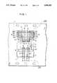
- FIG. 1is a plan view of a TAB package constituting a portion of a structure of a semiconductor device according to a preferred embodiment of the present invention
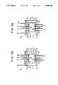
- FIGS. 2a to 2dare plan views for representing such conditions that the TAB packages on which LSI chips to be stacked have been packaged are cut off in a predetermined form for each stacked layer;
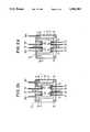
- FIG. 3is a sectional view for showing a packaging condition that the TAB package on which the respective LSI chips have been packaged is stacked;
- FIG. 4is a perspective view of a major portion of the TAB package.
- FIG. 5is a sectional view of the conventional high-density packaged semiconductor device.
- FIG. 1is a plan view of a TAB package constituting a portion of a structure of a semiconductor device according to one preferred embodiment of the present invention.
- FIGS. 3 and 4a description will be made to this preferred embodiment in which four chips of memory LSI chips are stacked.
- FIG. 1At least a device hole 3 and an outer lead hole 4 are opened on a resin film (film carrier tape) 1 such as polyimide and glass epoxy (epoxy containing a glass fiber), and inner leads 5 and 7 which are formed by copper foils and plated are arranged which a projected form on the device hole 3.
- a lead 100is constructed of the inner leads 5 and 7, and outer leads integrally formed with these inner leads.
- a region of the outer lead 8is divided into a plurality of outer leads 8a to 8h.
- a chip 2has eight electrodes to which eight inner leads have been connected respectively.
- FIG. 1represents such a condition that electrodes 6 and 10 of the LSI chip 2 have been connected to the inner leads 5 and 7.
- Both the LSI chip 2 and inner leads 5, 7make a junction between the leads 5, 7 and a bump (metal projection) formed on the electrodes 6 and 10 on the chip 2, or form a bump on the leads 5 and 7.
- These chips and inner leadsare connected by making a junction between this bump and electrodes 6 and 10.
- the leads 5 and 5' for processing the same signals of electrodes at the same position on the chip 2namely common terminals correspond to terminals of a power source and a clock signal, and are continuously formed in a single form via an inner lead region connected to the electrode of the LSI chip 2 and also a subsequent outer lead region.
- a lead for processing different signals at an electrode 10 at the same position on the chip 2, namely a non-common electrode terminal for selecting a chip used for inputting/ outputting signals into/from the respective chipsis formed as a single lead at least in an inner lead region, i.e., an inner lead 7.
- this leadis formed as lead groups (outer leads) 8a to 8h in an outer lead region 8 in which the inner lead 7 has been divided by the number of the chips to be stacked.
- a hole 9is formed on an arbitrary position of the film carrier tape 1.
- a single LSI chip 2is represented in FIG. 1, a plenty of chips shown in FIG. 1 have been mounted on the tape 1 in the longitudinal direction. That is to say, a plenty of LSI chips 2 are packaged on the inner leads 5 and 7 of the film carrier tap 1 in the longitudinal direction, and electrically inspected.
- a protective resin film(not shown) is formed on the chip 2, and is cut off in a predetermined form at a portion of, for example, a dot line "L" before mounted on the circuit board, so that each of TAB packages is formed.
- FIGS. 2a to 2dare plan views for representing such a condition that the film under the condition of FIG. 1 is cut off in a predetermined form, and the TAB packages of the respective layers, on which the LSI chips to be stacked have been packaged.
- TAB package "A" on which LSI chips to be stacked have been packagedall of the outer leads (8b, 8c, 8d, 8f, 8g and 8h) of the electrode 10.
- Other than the outer leads 8a and 8ehave been cut off (FIG. 2a.
- the outer leads 8a, 8c, 8d, 8e, 8g and 8h of the electrode 10 at the same position as in the chip "A”are cut off, and only the outer leads 8b and 8f remain (FIG. 2b).
- the outer leads 8c and 8gare left
- the outer leads 8d and 8hare left, the remaining leads are cut off (FIGS. 2c and 2d).
- the shapes of the cut outer lead 8are different from each other every stacked layer of the LSI chip.
- Such a selective cutting operation of the outer lead 8is simultaneously performed by utilizing, for instance, a punching die when each of the chips 2 is cut out from the film carrier 1 after the LSI chip 2 has been packaged on the film shown in FIG. 1. Otherwise, after the chip 2 has similarly been cut off in a predetermined shape with a preselected die, only the outer lead 8 may be cut at a different stage.
- the outer lead 8a, 8b, 8c, 8d, 8e, 8f, 8g and 8h conducted from the electrodes 10 of the respective packages, functioning as non-common electrodesare not overlapped under the stacked condition.
- signalscan be separately input/output into/from the outer leaders stacked under such a condition.
- FIG. 3is a sectional view for representing such a packaging condition that TAB packages on which LSI chips have been packaged are stacked.
- FIG. 4is a perspective view of a portion of a stacked package condition.
- a guide pin 50is inserted into a hole 9 so as to position an outer lead among each package when tape carrier packages are stacked, TAB packages "A" to "D” having packaged four LSI chips A, B, C, D are stacked and provided on a circuit board 30, and as previously described, the outer leads which have been conducted without any overlap are connected to each of electrode wiring patterns formed on the circuit board 30.
- TAB packages "A" to "D”having packaged four LSI chips A, B, C, D are stacked and provided on a circuit board 30, and as previously described, the outer leads which have been conducted without any overlap are connected to each of electrode wiring patterns formed on the circuit board 30.
- outer leads 8a, 8b, 8c, 8dare brought into such a condition that they are merely cut out from the film carrier 1 (under condition that the leads are conducted in the same direction as the chip plane), and the leads of the respective chips may be forming-processed, as represented in FIG. 3, by depressing the leads with, for instance, the pulse tool 51 when the respective chips are mounted on the circuit board 30.
- the leads 5' conducted from the common terminals of the respective LSI chipsare wholely connected to the electrode of the circuit board under such a condition that these leads are overlapped with each other at the same position.
- a plurality of extremely thin TAB packages on which the LSI chips have been packagedmay be easily stacked on the circuit board at the higher density. Then, except for the common terminals of the respective chips, the non-common terminals (outer leaders) may be conducted to the different positions on the circuit board. Furthermore, since the outer leads have been accomplished when the TAB packages are formed, no extra treatment is required when being packaged to the circuit board, and no work for employing other components is required.
- the above-described memory chipsare not limited to DRAMs, but the present invention may be applied to SRAM and ROM and the like. It is apparent that the present invention may be applied to components other than the memory chip. Then, the stack number of the LSI chips are not ristricted to four, but may be two or more according to the present invention.
- the semiconductor chipscan be readily stacked on the circuit board, and the lead terminals thereof can be simply connected to the circuit board according to the present invention. Since the package according to the present invention is manufactured by employing the TAB technique, a plurality of outer leads can be formed in a fine pitch by separating a single inner lead, and the unnecessary leads can be simply cut off. Also, in accordance with the present invention, since a plenty of chips can be processed with a package area required for at least a single chip even when these chips are mounted, there is a particular advantage that the packaging density can be considerably increased, and also a very useful technique can be achieved in an industrial field.
Landscapes
- Engineering & Computer Science (AREA)
- Microelectronics & Electronic Packaging (AREA)
- Power Engineering (AREA)
- Physics & Mathematics (AREA)
- Condensed Matter Physics & Semiconductors (AREA)
- General Physics & Mathematics (AREA)
- Computer Hardware Design (AREA)
- Lead Frames For Integrated Circuits (AREA)
Abstract
Description
The present invention relates to a semiconductor device having such a structure that a plurality of packages packaged in the TAB method are stacked.
Very recently, a great demand for a higher density of electronic appliances is made. To satisfy such a demand, an arrangement as shown in FIG. 5 has been employed. FIG. 5 is a sectional view of an example of a conventional semiconductor device manufactured by the high density packaging A predetermined wiring pattern and electrodes 21a and 21b are formed on both sides of acircuit board 20. Each of wiring patterns formed on either side is electrically connected by a through hole (not shown) with each other. Packagedsemiconductor chips circuit boards 20. In accordance with such a conventional structure, a packaging density thereof becomes at least two times higher than that of the same plane area by mounting the packages on both sides of thecircuit board 20.
In the conventional structure, however, since the packages are mounted on both sides of the circuit board in a plane form, only twice packaging density can be achieved. As a result, the more the number of the mounted chips increases, the higher the packaging area becomes. There is a problem that the higher density of the electronic appliances is impeded.
The present invention has been made in an attempt to solve the above-described problem, and has an object to provide a stack type semiconductor package capable of achieving more than two times higher packaging density.
Another object of the present invention is to provide such a structure that leads of stacked semiconductor devices can be readily connected to a board.
A still further object of the present invention is to provide a stack structure suitable for stacking a semiconductor memory device.
To solve the above-described subject, a structure of the present invention is that in an outer lead region connected to an inner lead which is connected to an electrode terminal of a semiconductor chip, the outer lead is divided into plural leads; a plurality of TAB packages for packaging the semiconductor chip are stacked; at least one of the divided leads remains at each of stacked stages; a predetermined quantity of other divided leads are cut off; and the stacked TAB packages are mounted on a circuit board.
In accordance with the above-described structure of the present invention, the semiconductor chips can be easily stacked on the circuit board with two or more stacked layers, and terminals other than the common terminals can be readily connected to the electrodes of the circuit board under this condition. As a result, it is possible to obtain such a package in which the semiconductor chips are stacked in a multi layer, and thus to realize more than twice packaging density.
FIG. 1 is a plan view of a TAB package constituting a portion of a structure of a semiconductor device according to a preferred embodiment of the present invention;
FIGS. 2a to 2d are plan views for representing such conditions that the TAB packages on which LSI chips to be stacked have been packaged are cut off in a predetermined form for each stacked layer;
FIG. 3 is a sectional view for showing a packaging condition that the TAB package on which the respective LSI chips have been packaged is stacked;
FIG. 4 is a perspective view of a major portion of the TAB package; and
FIG. 5 is a sectional view of the conventional high-density packaged semiconductor device.
In case that a plurality of LSI memory chips are mounted on the same circuit board, for electrodes commonly used for each chip such as a power source, a clock signal line, and the like, the same electrodes of these chips can be commonly connected to each other and to wining patterns formed on the circuit board. However, non-common electrodes such as electrodes for selecting chips are separately derived from the respective chips, and are required to be connected to specific wiring patterns formed on the circuit board. There exists such a subject when a plurality of LSI memory chips are stacked. A description will now be made to the following preferred embodiments according to the present invention, in which the connecting treatments of both the common electrodes and non-common electrodes have been considered.
FIG. 1 is a plan view of a TAB package constituting a portion of a structure of a semiconductor device according to one preferred embodiment of the present invention.
Referring now to FIGS. 3 and 4, a description will be made to this preferred embodiment in which four chips of memory LSI chips are stacked.
In FIG. 1, at least adevice hole 3 and anouter lead hole 4 are opened on a resin film (film carrier tape) 1 such as polyimide and glass epoxy (epoxy containing a glass fiber), andinner leads device hole 3. It should be noted that alead 100 is constructed of theinner leads outer lead 8 is divided into a plurality ofouter leads 8a to 8h. In the construction example shown in FIG. 1, achip 2 has eight electrodes to which eight inner leads have been connected respectively. FIG. 1 represents such a condition thatelectrodes LSI chip 2 have been connected to theinner leads LSI chip 2 andinner leads leads electrodes chip 2, or form a bump on theleads electrodes leads 5 and 5' for processing the same signals of electrodes at the same position on thechip 2, namely common terminals correspond to terminals of a power source and a clock signal, and are continuously formed in a single form via an inner lead region connected to the electrode of theLSI chip 2 and also a subsequent outer lead region. On the other hand, in each of the LSI chips to be stacked, a lead for processing different signals at anelectrode 10 at the same position on thechip 2, namely a non-common electrode terminal for selecting a chip used for inputting/ outputting signals into/from the respective chips, is formed as a single lead at least in an inner lead region, i.e., aninner lead 7. However, this lead is formed as lead groups (outer leads) 8a to 8h in anouter lead region 8 in which theinner lead 7 has been divided by the number of the chips to be stacked.
Ahole 9 is formed on an arbitrary position of the film carrier tape 1. It should be noted that although asingle LSI chip 2 is represented in FIG. 1, a plenty of chips shown in FIG. 1 have been mounted on the tape 1 in the longitudinal direction. That is to say, a plenty ofLSI chips 2 are packaged on theinner leads chip 2, and is cut off in a predetermined form at a portion of, for example, a dot line "L" before mounted on the circuit board, so that each of TAB packages is formed.
FIGS. 2a to 2d are plan views for representing such a condition that the film under the condition of FIG. 1 is cut off in a predetermined form, and the TAB packages of the respective layers, on which the LSI chips to be stacked have been packaged. In a TAB package "A" on which LSI chips to be stacked have been packaged, all of the outer leads (8b, 8c, 8d, 8f, 8g and 8h) of theelectrode 10. Other than theouter leads outer leads electrode 10 at the same position as in the chip "A" are cut off, and only theouter leads outer leads outer leads outer lead 8 are different from each other every stacked layer of the LSI chip. Such a selective cutting operation of theouter lead 8 is simultaneously performed by utilizing, for instance, a punching die when each of thechips 2 is cut out from the film carrier 1 after theLSI chip 2 has been packaged on the film shown in FIG. 1. Otherwise, after thechip 2 has similarly been cut off in a predetermined shape with a preselected die, only theouter lead 8 may be cut at a different stage.
When all of the respective TAB packages "A" to "D" having the structures shown in FIG. 2 are stacked, theouter lead electrodes 10 of the respective packages, functioning as non-common electrodes are not overlapped under the stacked condition. As a consequence, signals can be separately input/output into/from the outer leaders stacked under such a condition.
FIG. 3 is a sectional view for representing such a packaging condition that TAB packages on which LSI chips have been packaged are stacked. FIG. 4 is a perspective view of a portion of a stacked package condition. In this structure, a guide pin 50 is inserted into ahole 9 so as to position an outer lead among each package when tape carrier packages are stacked, TAB packages "A" to "D" having packaged four LSI chips A, B, C, D are stacked and provided on acircuit board 30, and as previously described, the outer leads which have been conducted without any overlap are connected to each of electrode wiring patterns formed on thecircuit board 30. In FIGS. 3 and 4, there are shown such conditions that the respective leads 8a, 8b, 8c and 8d are connected to the respective electrode wiring patterns 31a to 31d of the board. With respect to the connection in this case, a temperature is instantaneously increased by employing, for example, a pulse tool and a solder layer is reflown so as to make such a connection. Also, as to the formings of the leads of the stacked LSI chips, since the leads theirselves are thin and soft, they can be simply formed in various shapes. It should be noted that even when the forming process of theseouter leads pulse tool 51 when the respective chips are mounted on thecircuit board 30.
It should be noted that the leads 5' conducted from the common terminals of the respective LSI chips are wholely connected to the electrode of the circuit board under such a condition that these leads are overlapped with each other at the same position.
As previously, described, a plurality of extremely thin TAB packages on which the LSI chips have been packaged may be easily stacked on the circuit board at the higher density. Then, except for the common terminals of the respective chips, the non-common terminals (outer leaders) may be conducted to the different positions on the circuit board. Furthermore, since the outer leads have been accomplished when the TAB packages are formed, no extra treatment is required when being packaged to the circuit board, and no work for employing other components is required.
In the examples shown in FIGS. 3 and 4, when a semiconductor memory chip is employed as the chip, an instruction signal is first input into thelead 8a in case that a signal input/output operation is performed for a chip "A". As a result, the signal can be input into only the chip "A". Similarly, in case that a signal input/output operation is carried out for, for instance, a chip "0", an instruction signal is input by thelead 8d. Under such a way, each of the stacked chips can be freely selected by employing theleads 8a to 8d functioning as chip selection terminals.
When, for instance, 256K DRAM, 1M DRAM and 4M DRAM are employed as the chips of the structures shown in FIGS. 3 and 4, and four chips for each DRAM are stacked, memory packages each having a DRAM capacity of 1M, 4M and 16M bits can be obtained. Then, this package corresponds to a TAB package having a thickness of approximately 445 micrometers per a single and directly stacked, so that the very thin and compact package can be formed and only a single area is required for the entire package.
It should be noted that the above-described memory chips are not limited to DRAMs, but the present invention may be applied to SRAM and ROM and the like. It is apparent that the present invention may be applied to components other than the memory chip. Then, the stack number of the LSI chips are not ristricted to four, but may be two or more according to the present invention.
As apparent from the foregoing descriptions, the semiconductor chips can be readily stacked on the circuit board, and the lead terminals thereof can be simply connected to the circuit board according to the present invention. Since the package according to the present invention is manufactured by employing the TAB technique, a plurality of outer leads can be formed in a fine pitch by separating a single inner lead, and the unnecessary leads can be simply cut off. Also, in accordance with the present invention, since a plenty of chips can be processed with a package area required for at least a single chip even when these chips are mounted, there is a particular advantage that the packaging density can be considerably increased, and also a very useful technique can be achieved in an industrial field.
Claims (5)
1. A semiconductor device, comprising:
an outer lead region connected to an inner lead which is connected to an electrode terminal of a semiconductor chip, said outer lead region comprising plural divided leads each connected to said inner lead; a circuit board; a plurality of TAB packages, said semiconductor chip being packaged in said TAB packages, said TAB packages being stacked in plural layers; said stacked TAB packages being mounted on said circuit board; at least one of said plural divided leads being provided at each of said stacked layers and a predetermined number of said plural divided leads being cut out of each of said stacked layers.
2. A semiconductor device as claimed in claim 1, wherein the number of the plural leads which are continuous with said inner lead and divided at the outer lead region is equal to the number of leads of the stacked layers.
3. A semiconductor device as claimed in claim 1, wherein positions of the plural divided leads which are provided without being cut out at said stacked layers are different for each package of the respective stacked layers to avoid interfering with said at least one of said plural divided leads which is provided at each of said stacked layers.
4. A semiconductor device as claimed in claim 1, wherein a hole is formed in a resin tape adjacent to the outer lead region and a guide pin is inserted into said hole so as to position the plural outer leads between each package when the TAB packages are stacked.
5. A semiconductor device as claimed in claim 1, wherein said semiconductor chip corresponds to a memory chip, and the outer lead which has been divided into plural leads correspond to terminals for supplying chip selection instructing signals.
Applications Claiming Priority (2)
| Application Number | Priority Date | Filing Date | Title |
|---|---|---|---|
| JP1-036822 | 1989-02-15 | ||
| JP3682289 | 1989-02-15 |
Publications (1)
| Publication Number | Publication Date |
|---|---|
| US4996583Atrue US4996583A (en) | 1991-02-26 |
Family
ID=12480449
Family Applications (1)
| Application Number | Title | Priority Date | Filing Date |
|---|---|---|---|
| US07/477,542Expired - LifetimeUS4996583A (en) | 1989-02-15 | 1990-02-09 | Stack type semiconductor package |
Country Status (3)
| Country | Link |
|---|---|
| US (1) | US4996583A (en) |
| EP (1) | EP0383296B1 (en) |
| DE (1) | DE69031184T2 (en) |
Cited By (89)
| Publication number | Priority date | Publication date | Assignee | Title |
|---|---|---|---|---|
| US5198888A (en)* | 1987-12-28 | 1993-03-30 | Hitachi, Ltd. | Semiconductor stacked device |
| US5227995A (en)* | 1989-07-18 | 1993-07-13 | International Business Machines Corporation | High density semiconductor memory module using split finger lead frame |
| US5241454A (en)* | 1992-01-22 | 1993-08-31 | International Business Machines Corporation | Mutlilayered flexible circuit package |
| DE4239857A1 (en)* | 1992-11-27 | 1994-06-01 | Abb Research Ltd | Power semiconductor module with semiconductor chip having two main surfaces - has conductive tracks contacted by terminals on second main surfaces via flat contact strips |
| US5320611A (en)* | 1993-02-04 | 1994-06-14 | Peter M. Bonutti | Expandable cannula having longitudinal wire and method of use |
| US5334875A (en)* | 1987-12-28 | 1994-08-02 | Hitachi, Ltd. | Stacked semiconductor memory device and semiconductor memory module containing the same |
| US5420756A (en)* | 1992-06-19 | 1995-05-30 | Kabushiki Kaisha Toshiba | Memory card including stacked semiconductor memory elements located on a printed circuit board having a straight wiring pattern |
| US5490041A (en)* | 1993-11-15 | 1996-02-06 | Matsushita Electric Industrial Co., Ltd. | Semiconductor integrated circuit module and a semiconductor integrated circuit device stacking the same |
| US5514907A (en)* | 1995-03-21 | 1996-05-07 | Simple Technology Incorporated | Apparatus for stacking semiconductor chips |
| US5614760A (en)* | 1994-06-23 | 1997-03-25 | Sharp Kabushiki Kaisha | Tape carrier package semiconductor device |
| US5652462A (en)* | 1993-04-05 | 1997-07-29 | Matsushita Electric Industrial Co., Ltd. | Multilevel semiconductor integrated circuit device |
| US5657206A (en)* | 1994-06-23 | 1997-08-12 | Cubic Memory, Inc. | Conductive epoxy flip-chip package and method |
| US5661087A (en)* | 1994-06-23 | 1997-08-26 | Cubic Memory, Inc. | Vertical interconnect process for silicon segments |
| US5677569A (en)* | 1994-10-27 | 1997-10-14 | Samsung Electronics Co., Ltd. | Semiconductor multi-package stack |
| US5698895A (en)* | 1994-06-23 | 1997-12-16 | Cubic Memory, Inc. | Silicon segment programming method and apparatus |
| US5761028A (en)* | 1996-05-02 | 1998-06-02 | Chrysler Corporation | Transistor connection assembly having IGBT (X) cross ties |
| US5786628A (en)* | 1994-09-28 | 1998-07-28 | International Business Machines Corporation | Method and workpiece for connecting a thin layer to a monolithic electronic modules surface and associated module packaging |
| US5804004A (en)* | 1992-05-11 | 1998-09-08 | Nchip, Inc. | Stacked devices for multichip modules |
| US5891761A (en)* | 1994-06-23 | 1999-04-06 | Cubic Memory, Inc. | Method for forming vertical interconnect process for silicon segments with thermally conductive epoxy preform |
| US6069403A (en)* | 1998-10-06 | 2000-05-30 | Intersil Corporation | Power module with lowered inductance and reduced voltage overshoots |
| US6080596A (en)* | 1994-06-23 | 2000-06-27 | Cubic Memory Inc. | Method for forming vertical interconnect process for silicon segments with dielectric isolation |
| US6124633A (en)* | 1994-06-23 | 2000-09-26 | Cubic Memory | Vertical interconnect process for silicon segments with thermally conductive epoxy preform |
| US6221006B1 (en) | 1998-02-10 | 2001-04-24 | Artemis Medical Inc. | Entrapping apparatus and method for use |
| US20010005042A1 (en)* | 1992-12-11 | 2001-06-28 | Burns Carmen D. | Method of manufacturing a surface mount package |
| US6255726B1 (en) | 1994-06-23 | 2001-07-03 | Cubic Memory, Inc. | Vertical interconnect process for silicon segments with dielectric isolation |
| US6325816B1 (en) | 1998-08-19 | 2001-12-04 | Artemis Medical, Inc. | Target tissue localization method |
| US6342727B1 (en)* | 1997-05-26 | 2002-01-29 | Seiko Epson Corporation | Tape carrier device for a tab |
| US6380629B1 (en) | 1999-06-29 | 2002-04-30 | Hyundai Electronics Industries Co., Ltd. | Wafer level stack package and method of fabricating the same |
| US6448661B1 (en)* | 2001-02-09 | 2002-09-10 | Samsung Electornics Co., Ltd. | Three-dimensional multi-chip package having chip selection pads and manufacturing method thereof |
| US6451626B1 (en) | 2001-07-27 | 2002-09-17 | Charles W.C. Lin | Three-dimensional stacked semiconductor package |
| US20020142515A1 (en)* | 2001-03-27 | 2002-10-03 | Staktek Group, L.P. | Contact member stacking system and method |
| US6465893B1 (en) | 1990-09-24 | 2002-10-15 | Tessera, Inc. | Stacked chip assembly |
| US6479888B1 (en)* | 1999-02-17 | 2002-11-12 | Hitachi, Ltd. | Semiconductor device and a method of manufacturing the same |
| US6486549B1 (en) | 2001-11-10 | 2002-11-26 | Bridge Semiconductor Corporation | Semiconductor module with encapsulant base |
| US6486528B1 (en) | 1994-06-23 | 2002-11-26 | Vertical Circuits, Inc. | Silicon segment programming apparatus and three terminal fuse configuration |
| US20030107118A1 (en)* | 2001-10-09 | 2003-06-12 | Tessera, Inc. | Stacked packages |
| US6589813B1 (en) | 1999-06-28 | 2003-07-08 | Hyundai Electronics Industries Co., Ltd. | Chip size stack package and method of fabricating the same |
| US20030129121A1 (en)* | 2002-01-04 | 2003-07-10 | Conoco Inc. | Integrated oxidative dehydrogenation/carbon filament production process and reactor therefor |
| US6608763B1 (en) | 2000-09-15 | 2003-08-19 | Staktek Group L.P. | Stacking system and method |
| US20030199913A1 (en)* | 1998-02-10 | 2003-10-23 | Artemis Medical, Inc. | Occlusion, anchoring, tensioning and flow direction apparatus and methods for use |
| US6650009B2 (en)* | 2000-07-18 | 2003-11-18 | Siliconware Precision Industries Co., Ltd. | Structure of a multi chip module having stacked chips |
| US6692462B2 (en) | 1999-05-19 | 2004-02-17 | Mackenzie Andrew J. | System and method for establishing vascular access |
| US20040031972A1 (en)* | 2001-10-09 | 2004-02-19 | Tessera, Inc. | Stacked packages |
| US6703651B2 (en)* | 2000-09-06 | 2004-03-09 | Infineon Technologies Ag | Electronic device having stacked modules and method for producing it |
| US6716670B1 (en) | 2002-01-09 | 2004-04-06 | Bridge Semiconductor Corporation | Method of forming a three-dimensional stacked semiconductor package device |
| US6740981B2 (en) | 2000-03-27 | 2004-05-25 | Kabushiki Kaisha, Toshiba | Semiconductor device including memory unit and semiconductor module including memory units |
| US20040099938A1 (en)* | 2002-09-11 | 2004-05-27 | Tessera, Inc. | Assemblies having stacked semiconductor chips and methods of making same |
| US20040104470A1 (en)* | 2002-08-16 | 2004-06-03 | Tessera, Inc. | Microelectronic packages with self-aligning features |
| US6765287B1 (en) | 2001-07-27 | 2004-07-20 | Charles W. C. Lin | Three-dimensional stacked semiconductor package |
| US20040145054A1 (en)* | 2002-09-06 | 2004-07-29 | Tessera, Inc. | Components, methods and assemblies for stacked packages |
| US20040217461A1 (en)* | 2002-08-05 | 2004-11-04 | Tessera, Inc. | Microelectronic adaptors, assemblies and methods |
| US20040245617A1 (en)* | 2003-05-06 | 2004-12-09 | Tessera, Inc. | Dense multichip module |
| US6885106B1 (en) | 2001-01-11 | 2005-04-26 | Tessera, Inc. | Stacked microelectronic assemblies and methods of making same |
| US6897090B2 (en) | 1994-12-29 | 2005-05-24 | Tessera, Inc. | Method of making a compliant integrated circuit package |
| US20050161797A1 (en)* | 2001-10-03 | 2005-07-28 | Formfactor, Inc. | Multiple die interconnect system |
| US20050173796A1 (en)* | 2001-10-09 | 2005-08-11 | Tessera, Inc. | Microelectronic assembly having array including passive elements and interconnects |
| US20050194672A1 (en)* | 2003-11-04 | 2005-09-08 | Tessera, Inc. | Stacked packages and systems incorporating the same |
| US20050203565A1 (en)* | 2003-09-19 | 2005-09-15 | Rethy Csaba L. | Trocar insertion apparatus |
| US20050224952A1 (en)* | 2004-04-13 | 2005-10-13 | Al Vindasius | Three dimensional six surface conformal die coating |
| US20050245959A1 (en)* | 1999-05-19 | 2005-11-03 | Carlson John E | System and method for establishing vascular access |
| US20050258530A1 (en)* | 2004-04-13 | 2005-11-24 | Al Vindasius | Micropede stacked die component assembly |
| US7067911B1 (en) | 2000-10-13 | 2006-06-27 | Bridge Semiconductor Corporation | Three-dimensional stacked semiconductor package with metal pillar in encapsulant aperture |
| US7066741B2 (en) | 1999-09-24 | 2006-06-27 | Staktek Group L.P. | Flexible circuit connector for stacked chip module |
| US7129113B1 (en) | 2000-10-13 | 2006-10-31 | Bridge Semiconductor Corporation | Method of making a three-dimensional stacked semiconductor package with a metal pillar in an encapsulant aperture |
| US7190060B1 (en) | 2002-01-09 | 2007-03-13 | Bridge Semiconductor Corporation | Three-dimensional stacked semiconductor package device with bent and flat leads and method of making same |
| US20070096332A1 (en)* | 2003-05-28 | 2007-05-03 | Tomotoshi Satoh | Electronic component, module, module assembling method, module identification method and module environment setting method |
| US20070096266A1 (en)* | 2005-11-02 | 2007-05-03 | Cheemen Yu | High density three dimensional semiconductor die package |
| US7215018B2 (en) | 2004-04-13 | 2007-05-08 | Vertical Circuits, Inc. | Stacked die BGA or LGA component assembly |
| US7227249B1 (en) | 2003-12-24 | 2007-06-05 | Bridge Semiconductor Corporation | Three-dimensional stacked semiconductor package with chips on opposite sides of lead |
| US7262082B1 (en) | 2000-10-13 | 2007-08-28 | Bridge Semiconductor Corporation | Method of making a three-dimensional stacked semiconductor package with a metal pillar and a conductive interconnect in an encapsulant aperture |
| US20080042250A1 (en)* | 2006-08-18 | 2008-02-21 | Tessera, Inc. | Stacked microelectronic assemblies and methods therefor |
| US20080209511A1 (en)* | 2004-05-18 | 2008-08-28 | Silverbrook Research Pty Ltd | Authentication method for pharmaceutical products having coded packaging |
| US20080315407A1 (en)* | 2007-06-20 | 2008-12-25 | Vertical Circuits, Inc. | Three-dimensional circuitry formed on integrated circuit device using two-dimensional fabrication |
| US20090008795A1 (en)* | 2007-07-02 | 2009-01-08 | Tessera, Inc. | Stackable microelectronic device carriers, stacked device carriers and methods of making the same |
| US7494843B1 (en) | 2006-12-26 | 2009-02-24 | Bridge Semiconductor Corporation | Method of making a semiconductor chip assembly with thermal conductor and encapsulant grinding |
| US20090093850A1 (en)* | 2007-10-05 | 2009-04-09 | Tyco Healthcare Group Lp | Expanding seal anchor for single incision surgery |
| US20090179318A1 (en)* | 2008-01-10 | 2009-07-16 | Abounion Technology Corporation | Multi-channel stackable semiconductor device and method for fabricating the same, and stacking substrate applied to the semiconductor device |
| US20090206458A1 (en)* | 2008-02-19 | 2009-08-20 | Vertical Circuits, Inc. | Flat leadless packages and stacked leadless package assemblies |
| US20100140440A1 (en)* | 2008-12-10 | 2010-06-10 | Omnetics Connector Corporation | Alignment device for fine pitch connector leads |
| US7811863B1 (en) | 2006-10-26 | 2010-10-12 | Bridge Semiconductor Corporation | Method of making a semiconductor chip assembly with metal pillar and encapsulant grinding and heat sink attachment |
| US20110051385A1 (en)* | 2009-08-31 | 2011-03-03 | Gainteam Holdings Limited | High-density memory assembly |
| US7993983B1 (en) | 2003-11-17 | 2011-08-09 | Bridge Semiconductor Corporation | Method of making a semiconductor chip assembly with chip and encapsulant grinding |
| US7993329B2 (en) | 2002-08-13 | 2011-08-09 | Cook Medical Technologies Llc | ERCP catheter with a removable handle for lithotriptor compatible basket |
| US20110227207A1 (en)* | 2010-03-18 | 2011-09-22 | Alpha And Omega Semiconductor Incorporated | Stacked dual chip package and method of fabrication |
| US20110227205A1 (en)* | 2010-03-18 | 2011-09-22 | Jun Lu | Multi-layer lead frame package and method of fabrication |
| US8436429B2 (en) | 2011-05-29 | 2013-05-07 | Alpha & Omega Semiconductor, Inc. | Stacked power semiconductor device using dual lead frame and manufacturing method |
| USRE45463E1 (en) | 2003-11-12 | 2015-04-14 | Tessera, Inc. | Stacked microelectronic assemblies with central contacts |
| US10390817B2 (en) | 2007-02-13 | 2019-08-27 | P Tech, Llc | Tissue fixation system and method |
| CN114649319A (en)* | 2022-02-11 | 2022-06-21 | 广东汇芯半导体有限公司 | Module of combinable semiconductor circuit |
Families Citing this family (3)
| Publication number | Priority date | Publication date | Assignee | Title |
|---|---|---|---|---|
| EP0379592A4 (en)* | 1988-06-29 | 1991-06-19 | Matsushita Electric Industrial Co. Ltd. | Ic memory card |
| US5311401A (en)* | 1991-07-09 | 1994-05-10 | Hughes Aircraft Company | Stacked chip assembly and manufacturing method therefor |
| US5345363A (en)* | 1993-04-07 | 1994-09-06 | Intel Corporation | Method and apparatus of coupling a die to a lead frame with a tape automated bonded tape that has openings which expose portions of the tape leads |
Citations (3)
| Publication number | Priority date | Publication date | Assignee | Title |
|---|---|---|---|---|
| JPS59136963A (en)* | 1983-01-25 | 1984-08-06 | Sanyo Electric Co Ltd | Multilayer mounting structure of memory storage |
| JPS6163048A (en)* | 1984-09-04 | 1986-04-01 | Toshiba Corp | memory module |
| JPS62226307A (en)* | 1986-03-28 | 1987-10-05 | Toshiba Corp | robot equipment |
Family Cites Families (1)
| Publication number | Priority date | Publication date | Assignee | Title |
|---|---|---|---|---|
| EP0379592A4 (en)* | 1988-06-29 | 1991-06-19 | Matsushita Electric Industrial Co. Ltd. | Ic memory card |
- 1990
- 1990-02-09USUS07/477,542patent/US4996583A/ennot_activeExpired - Lifetime
- 1990-02-14DEDE69031184Tpatent/DE69031184T2/ennot_activeExpired - Fee Related
- 1990-02-14EPEP90102886Apatent/EP0383296B1/ennot_activeExpired - Lifetime
Patent Citations (3)
| Publication number | Priority date | Publication date | Assignee | Title |
|---|---|---|---|---|
| JPS59136963A (en)* | 1983-01-25 | 1984-08-06 | Sanyo Electric Co Ltd | Multilayer mounting structure of memory storage |
| JPS6163048A (en)* | 1984-09-04 | 1986-04-01 | Toshiba Corp | memory module |
| JPS62226307A (en)* | 1986-03-28 | 1987-10-05 | Toshiba Corp | robot equipment |
Cited By (160)
| Publication number | Priority date | Publication date | Assignee | Title |
|---|---|---|---|---|
| US5198888A (en)* | 1987-12-28 | 1993-03-30 | Hitachi, Ltd. | Semiconductor stacked device |
| US5334875A (en)* | 1987-12-28 | 1994-08-02 | Hitachi, Ltd. | Stacked semiconductor memory device and semiconductor memory module containing the same |
| US5227995A (en)* | 1989-07-18 | 1993-07-13 | International Business Machines Corporation | High density semiconductor memory module using split finger lead frame |
| US6465893B1 (en) | 1990-09-24 | 2002-10-15 | Tessera, Inc. | Stacked chip assembly |
| US5241454A (en)* | 1992-01-22 | 1993-08-31 | International Business Machines Corporation | Mutlilayered flexible circuit package |
| US5804004A (en)* | 1992-05-11 | 1998-09-08 | Nchip, Inc. | Stacked devices for multichip modules |
| US5420756A (en)* | 1992-06-19 | 1995-05-30 | Kabushiki Kaisha Toshiba | Memory card including stacked semiconductor memory elements located on a printed circuit board having a straight wiring pattern |
| DE4239857A1 (en)* | 1992-11-27 | 1994-06-01 | Abb Research Ltd | Power semiconductor module with semiconductor chip having two main surfaces - has conductive tracks contacted by terminals on second main surfaces via flat contact strips |
| US6919626B2 (en) | 1992-12-11 | 2005-07-19 | Staktek Group L.P. | High density integrated circuit module |
| US20010005042A1 (en)* | 1992-12-11 | 2001-06-28 | Burns Carmen D. | Method of manufacturing a surface mount package |
| US5320611A (en)* | 1993-02-04 | 1994-06-14 | Peter M. Bonutti | Expandable cannula having longitudinal wire and method of use |
| US5742097A (en)* | 1993-04-05 | 1998-04-21 | Matsushita Electric Industrial Co., Ltd. | Multilevel semiconductor integrated circuit device |
| US5652462A (en)* | 1993-04-05 | 1997-07-29 | Matsushita Electric Industrial Co., Ltd. | Multilevel semiconductor integrated circuit device |
| US5490041A (en)* | 1993-11-15 | 1996-02-06 | Matsushita Electric Industrial Co., Ltd. | Semiconductor integrated circuit module and a semiconductor integrated circuit device stacking the same |
| US6124633A (en)* | 1994-06-23 | 2000-09-26 | Cubic Memory | Vertical interconnect process for silicon segments with thermally conductive epoxy preform |
| US5614760A (en)* | 1994-06-23 | 1997-03-25 | Sharp Kabushiki Kaisha | Tape carrier package semiconductor device |
| US6486528B1 (en) | 1994-06-23 | 2002-11-26 | Vertical Circuits, Inc. | Silicon segment programming apparatus and three terminal fuse configuration |
| US5698895A (en)* | 1994-06-23 | 1997-12-16 | Cubic Memory, Inc. | Silicon segment programming method and apparatus |
| US5657206A (en)* | 1994-06-23 | 1997-08-12 | Cubic Memory, Inc. | Conductive epoxy flip-chip package and method |
| US5675180A (en)* | 1994-06-23 | 1997-10-07 | Cubic Memory, Inc. | Vertical interconnect process for silicon segments |
| US5837566A (en)* | 1994-06-23 | 1998-11-17 | Cubic Memory, Inc. | Vertical interconnect process for silicon segments |
| US5891761A (en)* | 1994-06-23 | 1999-04-06 | Cubic Memory, Inc. | Method for forming vertical interconnect process for silicon segments with thermally conductive epoxy preform |
| US5994170A (en)* | 1994-06-23 | 1999-11-30 | Cubic Memory, Inc. | Silicon segment programming method |
| US6255726B1 (en) | 1994-06-23 | 2001-07-03 | Cubic Memory, Inc. | Vertical interconnect process for silicon segments with dielectric isolation |
| US6080596A (en)* | 1994-06-23 | 2000-06-27 | Cubic Memory Inc. | Method for forming vertical interconnect process for silicon segments with dielectric isolation |
| US5661087A (en)* | 1994-06-23 | 1997-08-26 | Cubic Memory, Inc. | Vertical interconnect process for silicon segments |
| US6188126B1 (en) | 1994-06-23 | 2001-02-13 | Cubic Memory Inc. | Vertical interconnect process for silicon segments |
| US5786628A (en)* | 1994-09-28 | 1998-07-28 | International Business Machines Corporation | Method and workpiece for connecting a thin layer to a monolithic electronic modules surface and associated module packaging |
| US5677569A (en)* | 1994-10-27 | 1997-10-14 | Samsung Electronics Co., Ltd. | Semiconductor multi-package stack |
| US6897090B2 (en) | 1994-12-29 | 2005-05-24 | Tessera, Inc. | Method of making a compliant integrated circuit package |
| USRE36916E (en)* | 1995-03-21 | 2000-10-17 | Simple Technology Incorporated | Apparatus for stacking semiconductor chips |
| US5514907A (en)* | 1995-03-21 | 1996-05-07 | Simple Technology Incorporated | Apparatus for stacking semiconductor chips |
| US5761028A (en)* | 1996-05-02 | 1998-06-02 | Chrysler Corporation | Transistor connection assembly having IGBT (X) cross ties |
| US6342727B1 (en)* | 1997-05-26 | 2002-01-29 | Seiko Epson Corporation | Tape carrier device for a tab |
| US20030199913A1 (en)* | 1998-02-10 | 2003-10-23 | Artemis Medical, Inc. | Occlusion, anchoring, tensioning and flow direction apparatus and methods for use |
| US6695858B1 (en) | 1998-02-10 | 2004-02-24 | Artemis Medical, Inc. | Medical device and methods for use |
| US20030195537A1 (en)* | 1998-02-10 | 2003-10-16 | Artemis Medical, Inc. | Medical device and methods for use |
| US6221006B1 (en) | 1998-02-10 | 2001-04-24 | Artemis Medical Inc. | Entrapping apparatus and method for use |
| US6409742B1 (en) | 1998-08-19 | 2002-06-25 | Artemis Medical, Inc. | Target tissue localization device and method |
| US6325816B1 (en) | 1998-08-19 | 2001-12-04 | Artemis Medical, Inc. | Target tissue localization method |
| US6140152A (en)* | 1998-10-06 | 2000-10-31 | Intersil Corporation | Power module with lowered inductance and reduced voltage overshoots |
| US6069403A (en)* | 1998-10-06 | 2000-05-30 | Intersil Corporation | Power module with lowered inductance and reduced voltage overshoots |
| US7160760B2 (en) | 1999-02-17 | 2007-01-09 | Renesas Technology Corp. | Semiconductor device and a method of manufacturing the same |
| US6479888B1 (en)* | 1999-02-17 | 2002-11-12 | Hitachi, Ltd. | Semiconductor device and a method of manufacturing the same |
| US7812464B2 (en) | 1999-02-17 | 2010-10-12 | Renesas Electronics Corporation | Semiconductor device and a method of manufacturing for high output MOSFET |
| US20030038360A1 (en)* | 1999-02-17 | 2003-02-27 | Toshinori Hirashima | Semiconductor device and a method of manufacturing the same |
| US20070158819A1 (en)* | 1999-02-17 | 2007-07-12 | Toshinori Hirashima | Semiconductor device and a method of manufacturing the same |
| US20050023671A1 (en)* | 1999-02-17 | 2005-02-03 | Renesas Technology Corp. | Semiconductor device and a method of manufacturing the same |
| US6812554B2 (en) | 1999-02-17 | 2004-11-02 | Renesas Technology Corp. | Semiconductor device and a method of manufacturing the same |
| US20080211082A1 (en)* | 1999-02-17 | 2008-09-04 | Hitachi, Ltd. | Semiconductor device and a method of manufacturing the same |
| US7385279B2 (en) | 1999-02-17 | 2008-06-10 | Renesas Technology Corp. | Semiconductor device and a method of manufacturing the same |
| US6692462B2 (en) | 1999-05-19 | 2004-02-17 | Mackenzie Andrew J. | System and method for establishing vascular access |
| US20050245959A1 (en)* | 1999-05-19 | 2005-11-03 | Carlson John E | System and method for establishing vascular access |
| US20040093003A1 (en)* | 1999-05-19 | 2004-05-13 | Mackenzie Andrew J. | System and method for establishing vascular access |
| US20080243169A1 (en)* | 1999-05-19 | 2008-10-02 | Carlson John E | System and method for establishing vascular access |
| US20050245958A1 (en)* | 1999-05-19 | 2005-11-03 | Carlson John E | System and method for establishing vascular access |
| US6589813B1 (en) | 1999-06-28 | 2003-07-08 | Hyundai Electronics Industries Co., Ltd. | Chip size stack package and method of fabricating the same |
| US6828686B2 (en) | 1999-06-28 | 2004-12-07 | Hyundai Electronics Industries Co., Ltd. | Chip size stack package and method of fabricating the same |
| US6380629B1 (en) | 1999-06-29 | 2002-04-30 | Hyundai Electronics Industries Co., Ltd. | Wafer level stack package and method of fabricating the same |
| US7066741B2 (en) | 1999-09-24 | 2006-06-27 | Staktek Group L.P. | Flexible circuit connector for stacked chip module |
| US6740981B2 (en) | 2000-03-27 | 2004-05-25 | Kabushiki Kaisha, Toshiba | Semiconductor device including memory unit and semiconductor module including memory units |
| US6650009B2 (en)* | 2000-07-18 | 2003-11-18 | Siliconware Precision Industries Co., Ltd. | Structure of a multi chip module having stacked chips |
| US6703651B2 (en)* | 2000-09-06 | 2004-03-09 | Infineon Technologies Ag | Electronic device having stacked modules and method for producing it |
| US6608763B1 (en) | 2000-09-15 | 2003-08-19 | Staktek Group L.P. | Stacking system and method |
| US7067911B1 (en) | 2000-10-13 | 2006-06-27 | Bridge Semiconductor Corporation | Three-dimensional stacked semiconductor package with metal pillar in encapsulant aperture |
| US7129113B1 (en) | 2000-10-13 | 2006-10-31 | Bridge Semiconductor Corporation | Method of making a three-dimensional stacked semiconductor package with a metal pillar in an encapsulant aperture |
| US7262082B1 (en) | 2000-10-13 | 2007-08-28 | Bridge Semiconductor Corporation | Method of making a three-dimensional stacked semiconductor package with a metal pillar and a conductive interconnect in an encapsulant aperture |
| US6885106B1 (en) | 2001-01-11 | 2005-04-26 | Tessera, Inc. | Stacked microelectronic assemblies and methods of making same |
| US6448661B1 (en)* | 2001-02-09 | 2002-09-10 | Samsung Electornics Co., Ltd. | Three-dimensional multi-chip package having chip selection pads and manufacturing method thereof |
| US6806120B2 (en) | 2001-03-27 | 2004-10-19 | Staktek Group, L.P. | Contact member stacking system and method |
| US6462408B1 (en) | 2001-03-27 | 2002-10-08 | Staktek Group, L.P. | Contact member stacking system and method |
| US20020142515A1 (en)* | 2001-03-27 | 2002-10-03 | Staktek Group, L.P. | Contact member stacking system and method |
| US6794741B1 (en) | 2001-07-27 | 2004-09-21 | Bridge Semiconductor Corporation | Three-dimensional stacked semiconductor package with pillars in pillar cavities |
| US6765287B1 (en) | 2001-07-27 | 2004-07-20 | Charles W. C. Lin | Three-dimensional stacked semiconductor package |
| US6451626B1 (en) | 2001-07-27 | 2002-09-17 | Charles W.C. Lin | Three-dimensional stacked semiconductor package |
| US6509639B1 (en) | 2001-07-27 | 2003-01-21 | Charles W. C. Lin | Three-dimensional stacked semiconductor package |
| US7681309B2 (en)* | 2001-10-03 | 2010-03-23 | Formfactor, Inc. | Method for interconnecting an integrated circuit multiple die assembly |
| US20050161797A1 (en)* | 2001-10-03 | 2005-07-28 | Formfactor, Inc. | Multiple die interconnect system |
| US6897565B2 (en) | 2001-10-09 | 2005-05-24 | Tessera, Inc. | Stacked packages |
| US6977440B2 (en) | 2001-10-09 | 2005-12-20 | Tessera, Inc. | Stacked packages |
| US7335995B2 (en) | 2001-10-09 | 2008-02-26 | Tessera, Inc. | Microelectronic assembly having array including passive elements and interconnects |
| US20050173796A1 (en)* | 2001-10-09 | 2005-08-11 | Tessera, Inc. | Microelectronic assembly having array including passive elements and interconnects |
| US20040031972A1 (en)* | 2001-10-09 | 2004-02-19 | Tessera, Inc. | Stacked packages |
| US20030107118A1 (en)* | 2001-10-09 | 2003-06-12 | Tessera, Inc. | Stacked packages |
| US20040203190A1 (en)* | 2001-10-09 | 2004-10-14 | Tessera, Inc. | Stacked packages |
| US6913949B2 (en) | 2001-10-09 | 2005-07-05 | Tessera, Inc. | Stacked packages |
| US20060033216A1 (en)* | 2001-10-09 | 2006-02-16 | Tessera, Inc. | Stacked packages |
| US6486549B1 (en) | 2001-11-10 | 2002-11-26 | Bridge Semiconductor Corporation | Semiconductor module with encapsulant base |
| US20030129121A1 (en)* | 2002-01-04 | 2003-07-10 | Conoco Inc. | Integrated oxidative dehydrogenation/carbon filament production process and reactor therefor |
| US6716670B1 (en) | 2002-01-09 | 2004-04-06 | Bridge Semiconductor Corporation | Method of forming a three-dimensional stacked semiconductor package device |
| US7190060B1 (en) | 2002-01-09 | 2007-03-13 | Bridge Semiconductor Corporation | Three-dimensional stacked semiconductor package device with bent and flat leads and method of making same |
| US20040217461A1 (en)* | 2002-08-05 | 2004-11-04 | Tessera, Inc. | Microelectronic adaptors, assemblies and methods |
| US7993329B2 (en) | 2002-08-13 | 2011-08-09 | Cook Medical Technologies Llc | ERCP catheter with a removable handle for lithotriptor compatible basket |
| US7053485B2 (en) | 2002-08-16 | 2006-05-30 | Tessera, Inc. | Microelectronic packages with self-aligning features |
| US20040104470A1 (en)* | 2002-08-16 | 2004-06-03 | Tessera, Inc. | Microelectronic packages with self-aligning features |
| US7294928B2 (en) | 2002-09-06 | 2007-11-13 | Tessera, Inc. | Components, methods and assemblies for stacked packages |
| US7935569B2 (en) | 2002-09-06 | 2011-05-03 | Tessera, Inc. | Components, methods and assemblies for stacked packages |
| US20040145054A1 (en)* | 2002-09-06 | 2004-07-29 | Tessera, Inc. | Components, methods and assemblies for stacked packages |
| US20080042274A1 (en)* | 2002-09-06 | 2008-02-21 | Tessera, Inc. | Components, methods and assemblies for stacked packages |
| US7071547B2 (en) | 2002-09-11 | 2006-07-04 | Tessera, Inc. | Assemblies having stacked semiconductor chips and methods of making same |
| US20040099938A1 (en)* | 2002-09-11 | 2004-05-27 | Tessera, Inc. | Assemblies having stacked semiconductor chips and methods of making same |
| US20040245617A1 (en)* | 2003-05-06 | 2004-12-09 | Tessera, Inc. | Dense multichip module |
| US20070096332A1 (en)* | 2003-05-28 | 2007-05-03 | Tomotoshi Satoh | Electronic component, module, module assembling method, module identification method and module environment setting method |
| US20090131871A1 (en)* | 2003-09-19 | 2009-05-21 | Csaba Rethy | Trocar insertion apparatus |
| US7479150B2 (en) | 2003-09-19 | 2009-01-20 | Tyco Healthcare Group Lp | Trocar insertion apparatus |
| US20050203565A1 (en)* | 2003-09-19 | 2005-09-15 | Rethy Csaba L. | Trocar insertion apparatus |
| US20050194672A1 (en)* | 2003-11-04 | 2005-09-08 | Tessera, Inc. | Stacked packages and systems incorporating the same |
| US20100013108A1 (en)* | 2003-11-04 | 2010-01-21 | Tessera, Inc. | Stacked packages and microelectronic assemblies incorporating the same |
| US20070290316A1 (en)* | 2003-11-04 | 2007-12-20 | Tessera, Inc. | Stacked packages and systems incorporating the same |
| US7183643B2 (en) | 2003-11-04 | 2007-02-27 | Tessera, Inc. | Stacked packages and systems incorporating the same |
| US7589409B2 (en) | 2003-11-04 | 2009-09-15 | Tessera, Inc. | Stacked packages and microelectronic assemblies incorporating the same |
| US8704351B2 (en) | 2003-11-04 | 2014-04-22 | Tessera, Inc. | Stacked microelectronic assemblies |
| US9437582B2 (en) | 2003-11-04 | 2016-09-06 | Tessera, Inc. | Stacked microelectronic assemblies |
| USRE45463E1 (en) | 2003-11-12 | 2015-04-14 | Tessera, Inc. | Stacked microelectronic assemblies with central contacts |
| US7993983B1 (en) | 2003-11-17 | 2011-08-09 | Bridge Semiconductor Corporation | Method of making a semiconductor chip assembly with chip and encapsulant grinding |
| US7227249B1 (en) | 2003-12-24 | 2007-06-05 | Bridge Semiconductor Corporation | Three-dimensional stacked semiconductor package with chips on opposite sides of lead |
| US20050224952A1 (en)* | 2004-04-13 | 2005-10-13 | Al Vindasius | Three dimensional six surface conformal die coating |
| US7705432B2 (en) | 2004-04-13 | 2010-04-27 | Vertical Circuits, Inc. | Three dimensional six surface conformal die coating |
| US7535109B2 (en) | 2004-04-13 | 2009-05-19 | Vertical Circuits, Inc. | Die assembly having electrical interconnect |
| US7215018B2 (en) | 2004-04-13 | 2007-05-08 | Vertical Circuits, Inc. | Stacked die BGA or LGA component assembly |
| US20050258530A1 (en)* | 2004-04-13 | 2005-11-24 | Al Vindasius | Micropede stacked die component assembly |
| US20070284716A1 (en)* | 2004-04-13 | 2007-12-13 | Vertical Circuits, Inc. | Assembly Having Stacked Die Mounted On Substrate |
| US8357999B2 (en) | 2004-04-13 | 2013-01-22 | Vertical Circuits (Assignment For The Benefit Of Creditors), Llc | Assembly having stacked die mounted on substrate |
| US7245021B2 (en) | 2004-04-13 | 2007-07-17 | Vertical Circuits, Inc. | Micropede stacked die component assembly |
| US20070290377A1 (en)* | 2004-04-13 | 2007-12-20 | Vertical Circuits, Inc. | Three Dimensional Six Surface Conformal Die Coating |
| US8729690B2 (en) | 2004-04-13 | 2014-05-20 | Invensas Corporation | Assembly having stacked die mounted on substrate |
| US20080209511A1 (en)* | 2004-05-18 | 2008-08-28 | Silverbrook Research Pty Ltd | Authentication method for pharmaceutical products having coded packaging |
| US8653653B2 (en) | 2005-11-02 | 2014-02-18 | Sandisk Technologies Inc. | High density three dimensional semiconductor die package |
| US20070096266A1 (en)* | 2005-11-02 | 2007-05-03 | Cheemen Yu | High density three dimensional semiconductor die package |
| US20100102440A1 (en)* | 2005-11-02 | 2010-04-29 | Cheemen Yu | High density three dimensional semiconductor die package |
| US7663216B2 (en) | 2005-11-02 | 2010-02-16 | Sandisk Corporation | High density three dimensional semiconductor die package |
| US7545029B2 (en) | 2006-08-18 | 2009-06-09 | Tessera, Inc. | Stack microelectronic assemblies |
| US20080042250A1 (en)* | 2006-08-18 | 2008-02-21 | Tessera, Inc. | Stacked microelectronic assemblies and methods therefor |
| US7811863B1 (en) | 2006-10-26 | 2010-10-12 | Bridge Semiconductor Corporation | Method of making a semiconductor chip assembly with metal pillar and encapsulant grinding and heat sink attachment |
| US7494843B1 (en) | 2006-12-26 | 2009-02-24 | Bridge Semiconductor Corporation | Method of making a semiconductor chip assembly with thermal conductor and encapsulant grinding |
| US11801044B2 (en) | 2007-02-13 | 2023-10-31 | P Tech, Llc | Tissue fixation system and method |
| US12137898B2 (en) | 2007-02-13 | 2024-11-12 | P Tech, Llc | Tissue fixation system and method |
| US10390817B2 (en) | 2007-02-13 | 2019-08-27 | P Tech, Llc | Tissue fixation system and method |
| US10517584B1 (en) | 2007-02-13 | 2019-12-31 | P Tech, Llc | Tissue fixation system and method |
| US20080315407A1 (en)* | 2007-06-20 | 2008-12-25 | Vertical Circuits, Inc. | Three-dimensional circuitry formed on integrated circuit device using two-dimensional fabrication |
| US20090008795A1 (en)* | 2007-07-02 | 2009-01-08 | Tessera, Inc. | Stackable microelectronic device carriers, stacked device carriers and methods of making the same |
| US7763983B2 (en) | 2007-07-02 | 2010-07-27 | Tessera, Inc. | Stackable microelectronic device carriers, stacked device carriers and methods of making the same |
| US8795326B2 (en) | 2007-10-05 | 2014-08-05 | Covidien Lp | Expanding seal anchor for single incision surgery |
| US20090093850A1 (en)* | 2007-10-05 | 2009-04-09 | Tyco Healthcare Group Lp | Expanding seal anchor for single incision surgery |
| US9474518B2 (en) | 2007-10-05 | 2016-10-25 | Covidien Lp | Expanding seal anchor for single incision surgery |
| EP2081226A1 (en) | 2008-01-10 | 2009-07-22 | Abounion Technology Corporation | Multi-channel stackable semiconductor device and method for fabricating the same, and stacking substrate applied to the semiconductor device |
| US20090179318A1 (en)* | 2008-01-10 | 2009-07-16 | Abounion Technology Corporation | Multi-channel stackable semiconductor device and method for fabricating the same, and stacking substrate applied to the semiconductor device |
| US8159053B2 (en) | 2008-02-19 | 2012-04-17 | Vertical Circuits, Inc. | Flat leadless packages and stacked leadless package assemblies |
| US7843046B2 (en) | 2008-02-19 | 2010-11-30 | Vertical Circuits, Inc. | Flat leadless packages and stacked leadless package assemblies |
| US20090206458A1 (en)* | 2008-02-19 | 2009-08-20 | Vertical Circuits, Inc. | Flat leadless packages and stacked leadless package assemblies |
| US20110012246A1 (en)* | 2008-02-19 | 2011-01-20 | Vertical Circuits, Inc. | Flat Leadless Packages and Stacked Leadless Package Assemblies |
| US8225475B2 (en) | 2008-12-10 | 2012-07-24 | Omnetics Connector Corporation | Alignment device for fine pitch connector leads |
| US20100140440A1 (en)* | 2008-12-10 | 2010-06-10 | Omnetics Connector Corporation | Alignment device for fine pitch connector leads |
| US20110051385A1 (en)* | 2009-08-31 | 2011-03-03 | Gainteam Holdings Limited | High-density memory assembly |
| US20110227207A1 (en)* | 2010-03-18 | 2011-09-22 | Alpha And Omega Semiconductor Incorporated | Stacked dual chip package and method of fabrication |
| US8581376B2 (en) | 2010-03-18 | 2013-11-12 | Alpha & Omega Semiconductor Incorporated | Stacked dual chip package and method of fabrication |
| US8513784B2 (en) | 2010-03-18 | 2013-08-20 | Alpha & Omega Semiconductor Incorporated | Multi-layer lead frame package and method of fabrication |
| US20110227205A1 (en)* | 2010-03-18 | 2011-09-22 | Jun Lu | Multi-layer lead frame package and method of fabrication |
| US8436429B2 (en) | 2011-05-29 | 2013-05-07 | Alpha & Omega Semiconductor, Inc. | Stacked power semiconductor device using dual lead frame and manufacturing method |
| CN114649319A (en)* | 2022-02-11 | 2022-06-21 | 广东汇芯半导体有限公司 | Module of combinable semiconductor circuit |
Also Published As
| Publication number | Publication date |
|---|---|
| DE69031184T2 (en) | 1998-02-19 |
| EP0383296A2 (en) | 1990-08-22 |
| EP0383296B1 (en) | 1997-08-06 |
| EP0383296A3 (en) | 1992-03-04 |
| DE69031184D1 (en) | 1997-09-11 |
Similar Documents
| Publication | Publication Date | Title |
|---|---|---|
| US4996583A (en) | Stack type semiconductor package | |
| US5780925A (en) | Lead frame package for electronic devices | |
| US5514907A (en) | Apparatus for stacking semiconductor chips | |
| US6348728B1 (en) | Semiconductor device having a plurality of semiconductor elements interconnected by a redistribution layer | |
| JP2642359B2 (en) | Semiconductor device | |
| US7776652B2 (en) | Methods for stacking wire-bonded integrated circuit dice on flip-chip bonded integrated circuit dice | |
| US5061990A (en) | Semiconductor device and the manufacture thereof | |
| US6504244B2 (en) | Semiconductor device and semiconductor module using the same | |
| US6703651B2 (en) | Electronic device having stacked modules and method for producing it | |
| US6791166B1 (en) | Stackable lead frame package using exposed internal lead traces | |
| US5399904A (en) | Array type semiconductor device having insulating circuit board | |
| US6242285B1 (en) | Stacked package of semiconductor package units via direct connection between leads and stacking method therefor | |
| US6103548A (en) | Semiconductor device and method of manufacture | |
| US20100009499A1 (en) | Stacked microelectronic layer and module with three-axis channel t-connects | |
| KR100587061B1 (en) | Semiconductor package | |
| KR100276213B1 (en) | Piling-package of ic chips | |
| JPH0514427B2 (en) | ||
| KR100395797B1 (en) | Semiconductor chip having electrode pad arrangement suitable for chip stacking and a chip stacked package device comprising such chips | |
| KR100541798B1 (en) | Tag pattern formation method of semiconductor device | |
| KR100376884B1 (en) | Stack package | |
| JP2685534B2 (en) | Film carrier | |
| JPH03291960A (en) | Substrate for semiconductor-device lamination and laminated semiconductor device | |
| JPS60200559A (en) | memory module | |
| JPH01170028A (en) | electronic equipment | |
| JPH01170037A (en) | semiconductor equipment |
Legal Events
| Date | Code | Title | Description |
|---|---|---|---|
| AS | Assignment | Owner name:MATSUSHITA ELECTRIC INDUSTRIAL CO., LTD., JAPAN Free format text:ASSIGNMENT OF ASSIGNORS INTEREST.;ASSIGNOR:HATADA, KENZO;REEL/FRAME:005231/0623 Effective date:19900206 | |
| STCF | Information on status: patent grant | Free format text:PATENTED CASE | |
| FEPP | Fee payment procedure | Free format text:PAYOR NUMBER ASSIGNED (ORIGINAL EVENT CODE: ASPN); ENTITY STATUS OF PATENT OWNER: LARGE ENTITY | |
| FPAY | Fee payment | Year of fee payment:4 | |
| FPAY | Fee payment | Year of fee payment:8 | |
| FPAY | Fee payment | Year of fee payment:12 |