US4994412A - Self-centering electrode for power devices - Google Patents
Self-centering electrode for power devicesDownload PDFInfo
- Publication number
- US4994412A US4994412AUS07/477,397US47739790AUS4994412AUS 4994412 AUS4994412 AUS 4994412AUS 47739790 AUS47739790 AUS 47739790AUS 4994412 AUS4994412 AUS 4994412A
- Authority
- US
- United States
- Prior art keywords
- die
- bonding
- alignment means
- lead
- clip
- Prior art date
- Legal status (The legal status is an assumption and is not a legal conclusion. Google has not performed a legal analysis and makes no representation as to the accuracy of the status listed.)
- Expired - Lifetime
Links
Images


Classifications
- H—ELECTRICITY
- H01—ELECTRIC ELEMENTS
- H01L—SEMICONDUCTOR DEVICES NOT COVERED BY CLASS H10
- H01L24/00—Arrangements for connecting or disconnecting semiconductor or solid-state bodies; Methods or apparatus related thereto
- H01L24/01—Means for bonding being attached to, or being formed on, the surface to be connected, e.g. chip-to-package, die-attach, "first-level" interconnects; Manufacturing methods related thereto
- H01L24/34—Strap connectors, e.g. copper straps for grounding power devices; Manufacturing methods related thereto
- H01L24/39—Structure, shape, material or disposition of the strap connectors after the connecting process
- H01L24/40—Structure, shape, material or disposition of the strap connectors after the connecting process of an individual strap connector
- H—ELECTRICITY
- H01—ELECTRIC ELEMENTS
- H01L—SEMICONDUCTOR DEVICES NOT COVERED BY CLASS H10
- H01L23/00—Details of semiconductor or other solid state devices
- H01L23/48—Arrangements for conducting electric current to or from the solid state body in operation, e.g. leads, terminal arrangements ; Selection of materials therefor
- H01L23/488—Arrangements for conducting electric current to or from the solid state body in operation, e.g. leads, terminal arrangements ; Selection of materials therefor consisting of soldered or bonded constructions
- H01L23/495—Lead-frames or other flat leads
- H01L23/49537—Plurality of lead frames mounted in one device
- H—ELECTRICITY
- H01—ELECTRIC ELEMENTS
- H01L—SEMICONDUCTOR DEVICES NOT COVERED BY CLASS H10
- H01L23/00—Details of semiconductor or other solid state devices
- H01L23/48—Arrangements for conducting electric current to or from the solid state body in operation, e.g. leads, terminal arrangements ; Selection of materials therefor
- H01L23/488—Arrangements for conducting electric current to or from the solid state body in operation, e.g. leads, terminal arrangements ; Selection of materials therefor consisting of soldered or bonded constructions
- H01L23/495—Lead-frames or other flat leads
- H01L23/49541—Geometry of the lead-frame
- H01L23/49562—Geometry of the lead-frame for individual devices of subclass H10D
- H—ELECTRICITY
- H01—ELECTRIC ELEMENTS
- H01L—SEMICONDUCTOR DEVICES NOT COVERED BY CLASS H10
- H01L24/00—Arrangements for connecting or disconnecting semiconductor or solid-state bodies; Methods or apparatus related thereto
- H01L24/01—Means for bonding being attached to, or being formed on, the surface to be connected, e.g. chip-to-package, die-attach, "first-level" interconnects; Manufacturing methods related thereto
- H01L24/34—Strap connectors, e.g. copper straps for grounding power devices; Manufacturing methods related thereto
- H01L24/36—Structure, shape, material or disposition of the strap connectors prior to the connecting process
- H01L24/37—Structure, shape, material or disposition of the strap connectors prior to the connecting process of an individual strap connector
- H—ELECTRICITY
- H01—ELECTRIC ELEMENTS
- H01L—SEMICONDUCTOR DEVICES NOT COVERED BY CLASS H10
- H01L2224/00—Indexing scheme for arrangements for connecting or disconnecting semiconductor or solid-state bodies and methods related thereto as covered by H01L24/00
- H01L2224/01—Means for bonding being attached to, or being formed on, the surface to be connected, e.g. chip-to-package, die-attach, "first-level" interconnects; Manufacturing methods related thereto
- H01L2224/26—Layer connectors, e.g. plate connectors, solder or adhesive layers; Manufacturing methods related thereto
- H01L2224/2612—Auxiliary members for layer connectors, e.g. spacers
- H01L2224/26122—Auxiliary members for layer connectors, e.g. spacers being formed on the semiconductor or solid-state body to be connected
- H01L2224/26145—Flow barriers
- H—ELECTRICITY
- H01—ELECTRIC ELEMENTS
- H01L—SEMICONDUCTOR DEVICES NOT COVERED BY CLASS H10
- H01L2224/00—Indexing scheme for arrangements for connecting or disconnecting semiconductor or solid-state bodies and methods related thereto as covered by H01L24/00
- H01L2224/01—Means for bonding being attached to, or being formed on, the surface to be connected, e.g. chip-to-package, die-attach, "first-level" interconnects; Manufacturing methods related thereto
- H01L2224/26—Layer connectors, e.g. plate connectors, solder or adhesive layers; Manufacturing methods related thereto
- H01L2224/31—Structure, shape, material or disposition of the layer connectors after the connecting process
- H01L2224/32—Structure, shape, material or disposition of the layer connectors after the connecting process of an individual layer connector
- H01L2224/321—Disposition
- H01L2224/32151—Disposition the layer connector connecting between a semiconductor or solid-state body and an item not being a semiconductor or solid-state body, e.g. chip-to-substrate, chip-to-passive
- H01L2224/32221—Disposition the layer connector connecting between a semiconductor or solid-state body and an item not being a semiconductor or solid-state body, e.g. chip-to-substrate, chip-to-passive the body and the item being stacked
- H01L2224/32245—Disposition the layer connector connecting between a semiconductor or solid-state body and an item not being a semiconductor or solid-state body, e.g. chip-to-substrate, chip-to-passive the body and the item being stacked the item being metallic
- H—ELECTRICITY
- H01—ELECTRIC ELEMENTS
- H01L—SEMICONDUCTOR DEVICES NOT COVERED BY CLASS H10
- H01L2224/00—Indexing scheme for arrangements for connecting or disconnecting semiconductor or solid-state bodies and methods related thereto as covered by H01L24/00
- H01L2224/01—Means for bonding being attached to, or being formed on, the surface to be connected, e.g. chip-to-package, die-attach, "first-level" interconnects; Manufacturing methods related thereto
- H01L2224/34—Strap connectors, e.g. copper straps for grounding power devices; Manufacturing methods related thereto
- H01L2224/36—Structure, shape, material or disposition of the strap connectors prior to the connecting process
- H01L2224/37—Structure, shape, material or disposition of the strap connectors prior to the connecting process of an individual strap connector
- H01L2224/37001—Core members of the connector
- H01L2224/37099—Material
- H01L2224/371—Material with a principal constituent of the material being a metal or a metalloid, e.g. boron [B], silicon [Si], germanium [Ge], arsenic [As], antimony [Sb], tellurium [Te] and polonium [Po], and alloys thereof
- H01L2224/37138—Material with a principal constituent of the material being a metal or a metalloid, e.g. boron [B], silicon [Si], germanium [Ge], arsenic [As], antimony [Sb], tellurium [Te] and polonium [Po], and alloys thereof the principal constituent melting at a temperature of greater than or equal to 950°C and less than 1550°C
- H01L2224/37147—Copper [Cu] as principal constituent
- H—ELECTRICITY
- H01—ELECTRIC ELEMENTS
- H01L—SEMICONDUCTOR DEVICES NOT COVERED BY CLASS H10
- H01L2224/00—Indexing scheme for arrangements for connecting or disconnecting semiconductor or solid-state bodies and methods related thereto as covered by H01L24/00
- H01L2224/01—Means for bonding being attached to, or being formed on, the surface to be connected, e.g. chip-to-package, die-attach, "first-level" interconnects; Manufacturing methods related thereto
- H01L2224/34—Strap connectors, e.g. copper straps for grounding power devices; Manufacturing methods related thereto
- H01L2224/39—Structure, shape, material or disposition of the strap connectors after the connecting process
- H01L2224/40—Structure, shape, material or disposition of the strap connectors after the connecting process of an individual strap connector
- H01L2224/4005—Shape
- H01L2224/4009—Loop shape
- H01L2224/40091—Arched
- H—ELECTRICITY
- H01—ELECTRIC ELEMENTS
- H01L—SEMICONDUCTOR DEVICES NOT COVERED BY CLASS H10
- H01L2224/00—Indexing scheme for arrangements for connecting or disconnecting semiconductor or solid-state bodies and methods related thereto as covered by H01L24/00
- H01L2224/01—Means for bonding being attached to, or being formed on, the surface to be connected, e.g. chip-to-package, die-attach, "first-level" interconnects; Manufacturing methods related thereto
- H01L2224/34—Strap connectors, e.g. copper straps for grounding power devices; Manufacturing methods related thereto
- H01L2224/39—Structure, shape, material or disposition of the strap connectors after the connecting process
- H01L2224/40—Structure, shape, material or disposition of the strap connectors after the connecting process of an individual strap connector
- H01L2224/4005—Shape
- H01L2224/4009—Loop shape
- H01L2224/40095—Kinked
- H—ELECTRICITY
- H01—ELECTRIC ELEMENTS
- H01L—SEMICONDUCTOR DEVICES NOT COVERED BY CLASS H10
- H01L2224/00—Indexing scheme for arrangements for connecting or disconnecting semiconductor or solid-state bodies and methods related thereto as covered by H01L24/00
- H01L2224/01—Means for bonding being attached to, or being formed on, the surface to be connected, e.g. chip-to-package, die-attach, "first-level" interconnects; Manufacturing methods related thereto
- H01L2224/34—Strap connectors, e.g. copper straps for grounding power devices; Manufacturing methods related thereto
- H01L2224/39—Structure, shape, material or disposition of the strap connectors after the connecting process
- H01L2224/40—Structure, shape, material or disposition of the strap connectors after the connecting process of an individual strap connector
- H01L2224/401—Disposition
- H01L2224/40151—Connecting between a semiconductor or solid-state body and an item not being a semiconductor or solid-state body, e.g. chip-to-substrate, chip-to-passive
- H01L2224/40221—Connecting between a semiconductor or solid-state body and an item not being a semiconductor or solid-state body, e.g. chip-to-substrate, chip-to-passive the body and the item being stacked
- H01L2224/40245—Connecting between a semiconductor or solid-state body and an item not being a semiconductor or solid-state body, e.g. chip-to-substrate, chip-to-passive the body and the item being stacked the item being metallic
- H—ELECTRICITY
- H01—ELECTRIC ELEMENTS
- H01L—SEMICONDUCTOR DEVICES NOT COVERED BY CLASS H10
- H01L2224/00—Indexing scheme for arrangements for connecting or disconnecting semiconductor or solid-state bodies and methods related thereto as covered by H01L24/00
- H01L2224/74—Apparatus for manufacturing arrangements for connecting or disconnecting semiconductor or solid-state bodies and for methods related thereto
- H01L2224/77—Apparatus for connecting with strap connectors
- H01L2224/7725—Means for applying energy, e.g. heating means
- H01L2224/77272—Oven
- H—ELECTRICITY
- H01—ELECTRIC ELEMENTS
- H01L—SEMICONDUCTOR DEVICES NOT COVERED BY CLASS H10
- H01L2224/00—Indexing scheme for arrangements for connecting or disconnecting semiconductor or solid-state bodies and methods related thereto as covered by H01L24/00
- H01L2224/80—Methods for connecting semiconductor or other solid state bodies using means for bonding being attached to, or being formed on, the surface to be connected
- H01L2224/83—Methods for connecting semiconductor or other solid state bodies using means for bonding being attached to, or being formed on, the surface to be connected using a layer connector
- H01L2224/838—Bonding techniques
- H01L2224/83801—Soldering or alloying
- H—ELECTRICITY
- H01—ELECTRIC ELEMENTS
- H01L—SEMICONDUCTOR DEVICES NOT COVERED BY CLASS H10
- H01L2224/00—Indexing scheme for arrangements for connecting or disconnecting semiconductor or solid-state bodies and methods related thereto as covered by H01L24/00
- H01L2224/80—Methods for connecting semiconductor or other solid state bodies using means for bonding being attached to, or being formed on, the surface to be connected
- H01L2224/84—Methods for connecting semiconductor or other solid state bodies using means for bonding being attached to, or being formed on, the surface to be connected using a strap connector
- H01L2224/8434—Bonding interfaces of the connector
- H01L2224/84345—Shape, e.g. interlocking features
- H—ELECTRICITY
- H01—ELECTRIC ELEMENTS
- H01L—SEMICONDUCTOR DEVICES NOT COVERED BY CLASS H10
- H01L2224/00—Indexing scheme for arrangements for connecting or disconnecting semiconductor or solid-state bodies and methods related thereto as covered by H01L24/00
- H01L2224/80—Methods for connecting semiconductor or other solid state bodies using means for bonding being attached to, or being formed on, the surface to be connected
- H01L2224/84—Methods for connecting semiconductor or other solid state bodies using means for bonding being attached to, or being formed on, the surface to be connected using a strap connector
- H01L2224/8438—Bonding interfaces outside the semiconductor or solid-state body
- H01L2224/84385—Shape, e.g. interlocking features
- H—ELECTRICITY
- H01—ELECTRIC ELEMENTS
- H01L—SEMICONDUCTOR DEVICES NOT COVERED BY CLASS H10
- H01L2224/00—Indexing scheme for arrangements for connecting or disconnecting semiconductor or solid-state bodies and methods related thereto as covered by H01L24/00
- H01L2224/80—Methods for connecting semiconductor or other solid state bodies using means for bonding being attached to, or being formed on, the surface to be connected
- H01L2224/84—Methods for connecting semiconductor or other solid state bodies using means for bonding being attached to, or being formed on, the surface to be connected using a strap connector
- H01L2224/848—Bonding techniques
- H01L2224/84801—Soldering or alloying
- H—ELECTRICITY
- H01—ELECTRIC ELEMENTS
- H01L—SEMICONDUCTOR DEVICES NOT COVERED BY CLASS H10
- H01L24/00—Arrangements for connecting or disconnecting semiconductor or solid-state bodies; Methods or apparatus related thereto
- H01L24/80—Methods for connecting semiconductor or other solid state bodies using means for bonding being attached to, or being formed on, the surface to be connected
- H01L24/84—Methods for connecting semiconductor or other solid state bodies using means for bonding being attached to, or being formed on, the surface to be connected using a strap connector
- H—ELECTRICITY
- H01—ELECTRIC ELEMENTS
- H01L—SEMICONDUCTOR DEVICES NOT COVERED BY CLASS H10
- H01L2924/00—Indexing scheme for arrangements or methods for connecting or disconnecting semiconductor or solid-state bodies as covered by H01L24/00
- H01L2924/01—Chemical elements
- H01L2924/01006—Carbon [C]
- H—ELECTRICITY
- H01—ELECTRIC ELEMENTS
- H01L—SEMICONDUCTOR DEVICES NOT COVERED BY CLASS H10
- H01L2924/00—Indexing scheme for arrangements or methods for connecting or disconnecting semiconductor or solid-state bodies as covered by H01L24/00
- H01L2924/01—Chemical elements
- H01L2924/01013—Aluminum [Al]
- H—ELECTRICITY
- H01—ELECTRIC ELEMENTS
- H01L—SEMICONDUCTOR DEVICES NOT COVERED BY CLASS H10
- H01L2924/00—Indexing scheme for arrangements or methods for connecting or disconnecting semiconductor or solid-state bodies as covered by H01L24/00
- H01L2924/01—Chemical elements
- H01L2924/01014—Silicon [Si]
- H—ELECTRICITY
- H01—ELECTRIC ELEMENTS
- H01L—SEMICONDUCTOR DEVICES NOT COVERED BY CLASS H10
- H01L2924/00—Indexing scheme for arrangements or methods for connecting or disconnecting semiconductor or solid-state bodies as covered by H01L24/00
- H01L2924/01—Chemical elements
- H01L2924/01027—Cobalt [Co]
- H—ELECTRICITY
- H01—ELECTRIC ELEMENTS
- H01L—SEMICONDUCTOR DEVICES NOT COVERED BY CLASS H10
- H01L2924/00—Indexing scheme for arrangements or methods for connecting or disconnecting semiconductor or solid-state bodies as covered by H01L24/00
- H01L2924/01—Chemical elements
- H01L2924/01029—Copper [Cu]
- H—ELECTRICITY
- H01—ELECTRIC ELEMENTS
- H01L—SEMICONDUCTOR DEVICES NOT COVERED BY CLASS H10
- H01L2924/00—Indexing scheme for arrangements or methods for connecting or disconnecting semiconductor or solid-state bodies as covered by H01L24/00
- H01L2924/01—Chemical elements
- H01L2924/01033—Arsenic [As]
- H—ELECTRICITY
- H01—ELECTRIC ELEMENTS
- H01L—SEMICONDUCTOR DEVICES NOT COVERED BY CLASS H10
- H01L2924/00—Indexing scheme for arrangements or methods for connecting or disconnecting semiconductor or solid-state bodies as covered by H01L24/00
- H01L2924/01—Chemical elements
- H01L2924/01047—Silver [Ag]
- H—ELECTRICITY
- H01—ELECTRIC ELEMENTS
- H01L—SEMICONDUCTOR DEVICES NOT COVERED BY CLASS H10
- H01L2924/00—Indexing scheme for arrangements or methods for connecting or disconnecting semiconductor or solid-state bodies as covered by H01L24/00
- H01L2924/01—Chemical elements
- H01L2924/01074—Tungsten [W]
- H—ELECTRICITY
- H01—ELECTRIC ELEMENTS
- H01L—SEMICONDUCTOR DEVICES NOT COVERED BY CLASS H10
- H01L2924/00—Indexing scheme for arrangements or methods for connecting or disconnecting semiconductor or solid-state bodies as covered by H01L24/00
- H01L2924/01—Chemical elements
- H01L2924/01082—Lead [Pb]
- H—ELECTRICITY
- H01—ELECTRIC ELEMENTS
- H01L—SEMICONDUCTOR DEVICES NOT COVERED BY CLASS H10
- H01L2924/00—Indexing scheme for arrangements or methods for connecting or disconnecting semiconductor or solid-state bodies as covered by H01L24/00
- H01L2924/10—Details of semiconductor or other solid state devices to be connected
- H01L2924/11—Device type
- H01L2924/13—Discrete devices, e.g. 3 terminal devices
- H01L2924/1301—Thyristor
- H—ELECTRICITY
- H01—ELECTRIC ELEMENTS
- H01L—SEMICONDUCTOR DEVICES NOT COVERED BY CLASS H10
- H01L2924/00—Indexing scheme for arrangements or methods for connecting or disconnecting semiconductor or solid-state bodies as covered by H01L24/00
- H01L2924/10—Details of semiconductor or other solid state devices to be connected
- H01L2924/11—Device type
- H01L2924/14—Integrated circuits
- H—ELECTRICITY
- H01—ELECTRIC ELEMENTS
- H01L—SEMICONDUCTOR DEVICES NOT COVERED BY CLASS H10
- H01L2924/00—Indexing scheme for arrangements or methods for connecting or disconnecting semiconductor or solid-state bodies as covered by H01L24/00
- H01L2924/19—Details of hybrid assemblies other than the semiconductor or other solid state devices to be connected
- H01L2924/1901—Structure
- H01L2924/1904—Component type
- H01L2924/19041—Component type being a capacitor
- H—ELECTRICITY
- H01—ELECTRIC ELEMENTS
- H01L—SEMICONDUCTOR DEVICES NOT COVERED BY CLASS H10
- H01L2924/00—Indexing scheme for arrangements or methods for connecting or disconnecting semiconductor or solid-state bodies as covered by H01L24/00
- H01L2924/19—Details of hybrid assemblies other than the semiconductor or other solid state devices to be connected
- H01L2924/1901—Structure
- H01L2924/1904—Component type
- H01L2924/19043—Component type being a resistor
- Y—GENERAL TAGGING OF NEW TECHNOLOGICAL DEVELOPMENTS; GENERAL TAGGING OF CROSS-SECTIONAL TECHNOLOGIES SPANNING OVER SEVERAL SECTIONS OF THE IPC; TECHNICAL SUBJECTS COVERED BY FORMER USPC CROSS-REFERENCE ART COLLECTIONS [XRACs] AND DIGESTS
- Y10—TECHNICAL SUBJECTS COVERED BY FORMER USPC
- Y10T—TECHNICAL SUBJECTS COVERED BY FORMER US CLASSIFICATION
- Y10T29/00—Metal working
- Y10T29/49—Method of mechanical manufacture
- Y10T29/49002—Electrical device making
- Y10T29/49117—Conductor or circuit manufacturing
- Y10T29/49121—Beam lead frame or beam lead device
Definitions
- This inventionrelates in general to electronic devices and, more particularly, to improved means and methods for providing leads to semiconductor or other electronic chips.
- device or devicesare intended to refer to all kinds of electronic devices and integrated circuits which use connection means and leads of the sort described herein, including but not limited to semiconductor based devices.
- Wire bonding of thin wires and tab bonding of metal foilsare examples of techniques commonly used for signal processing devices. Such wires or foils generally carry only microamperes or milliamperes, are typically a fraction of a mil to a few mils thick, and are generally welded directly to the bonding pads on the device.
- the leads bonded to the devicemust be more robust. It is commonplace to use metal leads that are of the order of ten to hundreds of mils thick. They are frequently attached by soldering to the bonding areas on the device.
- solder or soldersare intended to include any electrically conductive attachment material which is semi-solid or at least partially liquid at some time during the lead attachment process.
- Non-limiting examplesare conventional metal or metal alloys or metal loaded epoxies or other conductive plastics and the like.
- chip or dieare intended to refer to electronic elements such as but not limited to diodes, transistors, thyristors, integrated circuits, resistors, capacitors and the like having at least one bonding region or pad thereon.
- an electronic chiphaving a first surface for attachment to a lead means and a second surface with a bonding pad thereon for receiving a connection means
- a lead meanshaving a first portion for receiving the electronic chip and a second portion including a first alignment means for alignment of the connection means
- a connection meansfor connecting the lead means to the electronic chip
- the connection meanshas a first portion for coupling to the bonding pad and a second portion with a second alignment means which mates with the first alignment means for aligning the connection means between the lead means and the bonding pad.
- connection meansIt is desirable to attach the bonding pad to the first portion of the connection means with a first solder, to attach the first and second alignment means with a second solder, and to attach the electronic chip and the first portion of the lead means with a third solder.
- the first, second and also preferably the third soldersshould have a controllable state during which the solders are at least partially liquid so that the die and connection means may be floated thereon to self-align to each other and to the lead means.
- the first portion of the connection meansis supported by the bonding pad and the second portion of the connection means is supported by the first alignment means.
- the first and second alignment meansconveniently have the form of mating depressions or protrusions in, respectively, the lead means and the connection means.
- the mating depressions or protrusionsare preferably of such a shape as to allow lateral or longitudinal motion or vertical rotation of the connection means with respect to the lead means, but not permit horizontal rotation of the connection means.
- a devicesuch as is described above and containing an electronic element therein, is conveniently obtained by steps comprising, supplying a support member for receiving the electronic element, supplying a lead member having a first alignment means for receiving a connection means with a mating second alignment means therein for mutually aligning the lead member and the connection means, supplying the connection means with the second alignment means for mating with the first alignment means and having a first attachment means for coupling to the electronic element, providing a first bonding material between the support member and the electronic element, providing a second bonding material between the first and second alignment means, and providing a third bonding material between the attachment means and the electronic element, temporarily floating the connection means on the second and third bonding material, and thereafter solidifying the second and third bonding material.
- the first bonding materialmay be provided before the second or third bonding material or simultaneously with the second bonding material or the second and third bonding materials maybe provided simultaneously.
- connection meansit is desirable to temporarily float the electronic element on the first bonding material at the same time as the connection means is floated on the first and second bonding materials so that the electronic element and the connection means align with each other and with the support member and lead member, controlled by the alignment means on the lead member and the connection means.
- first alignment meansas a first depression or protrusion in the lead member and the second alignment means as a mating second depression or protrusion in the connection means, further, place the second alignment means in the first alignment means separated by the second bonding material where they are retained by gravity and surface tension until the second bonding material is solidified. It is further desirable to agitate at least the support member during the floating step.
- connection meansThe arrangement of the lead member, support member and connection means, and the choice of and the relative amounts of the three bonding materials should be such that the surface tension forces in the liquified bonding materials align the connection means to the lead member, center the bonding pad on the die under the attachment portion of the connection means, and substantially center the die and attachment portion of the connection means above the die bond region of the die support member. This provides automatic alignment of the parts.
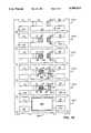
- FIG. 1is a top and partial cut-away view and FIG. 2 is a partial cross-sectional view, as indicated on FIG. 1, of a portion of an electronic device according to the prior art.
- FIG. 3is a top view and FIGS. 4-5 are partial cross-sectional views, as indicated on FIG. 3, of a portion of an electronic device according to the present invention.
- FIG. 6is a top and partial cutaway view and FIG. 7 is a partial cross-sectional view, as indicated in FIG. 6, of a portion of an electronic device according to a further embodiment of the present invention.
- FIG. 8is a top and partial cutaway view and FIG. 9 is a partial cross-sectional view, as indicated in FIG. 8, of a portion of an electronic device according to a still further embodiment of the present invention.
- FIG. 10is a top plan view of a portion of an electronic leadframe having multiple sections and showing and example of the method of the present invention.
- FIGS. 1shows a partial cut-away top view and FIG. 2 shows a cross-sectional view of portion 10 of a prior art electronic device, for example a semiconductor device, comprising die support means 12 having die bond region 13, electronic die (e.g., semiconductor chip) 16, and conductive electrode 14.
- Die support lead 12 and contact lead 14are typically made of metals well known in the art. Copper is an example.
- Die 16is attached to support 12 by attachment means 19. Contact 22 on die 16 is bonded to lead 14 by bonding material 26, for example, a solder. In the example shown, die 16 has raised dielectric 18 surrounding contact 22, but this is not essential.
- die support 12 and lead 14are generally made of comparatively thick metals, as for example, copper or KovarTM or other metals having thicknesses in the order of 10 to hundreds of mils (0.25 to several millimeters).
- Such leadsare comparatively stiff and alignment of the die flag, the die and the contact lead can be a problem in manufacturing.
- the prior art arrangement shown in FIGS. 1-2has the additional disadvantage that it promotes run-out of solder 26 onto the upper surface of dielectric 18, which is undesirable for good manufacturing yield and reliability.
- FIGS. 1-2The prior art arrangement of FIGS. 1-2 is also difficult to assemble since leads 12 and 14 must overlap with die 16 in between. In these circumstances, after die 16 is mounted on die flag 13, lead 14 must either be folded over from another part of the leadframe or provided separately. Both operations require additional steps and care must be taken to properly align lead 14 above die 16 and die flag 13.
- FIG. 5is a cross-sectional view similar to FIG. 4 but illustrating a further embodiment.
- attachment means 20may be conductive or insulating, but conductive solder is frequently used when die support 12, 13 is also intended to serve as one of the electrical leads of the device coupled to die 16.
- Lead 30, 50is provided extending toward die 16 and is intended to serve as an external connection to die 16. Conveniently located near the end of lead 30, 50 closest to die 16 is alignment means 32, 52. In the example shown in FIGS. 3-5, alignment means 32, 52 has the shape of a depression in lead 30, 50 but other shapes such as a protrusion could also be used. In FIGS. 3-4, alignment means 32 has the shape of a substantially hemi-cylindrical groove or other rounded two dimensional shape whose long dimension extends transverse to the direction from lead 30 toward die 16. In FIG.
- alignment means 52has a the shape of a two dimensional notch or fold-like depression whose long dimension extends transverse to the direction from lead 50 toward die 16 While alignment means 32, 42 and 52, 62 are shown as being convex downward, they could also be convex upward, i.e., bumps or protrusions rather than depressions.
- connection means or clip 40, 60extends from lead 30, 50 to contact region 22 on die 16.
- Connection clip or means 40, 60has alignment means 42, 62 at a first end which mates with alignment means 32, 52 of lead 30, 50 and, at a second end, has attachment means 46, 66 which is coupled to die contact or bonding pad 22.
- the shapes of alignment means 42, 62are such that they engage alignment means 32, 52. As can be seen in FIG.
- connection means 40, 60to move transverse to the direction extending from lead 30, 50 toward die contact 22 on die 16, but restrain movement of clip 40, 60 relative to lead 30, 50 and die contact 22 in the direction toward die contact 22 and restrain horizontal (azimuthal) rotation of connection means 40, 60 relative to lead 30, 50 or bonding pad 22 in the plane of FIG. 3.
- connection means 40, 60is able to rotate during assembly in the vertical plane, that is in the plane of FIGS. 4- 5. This is desirable since it permits substantial variations in the thickness of die 16 to be accommodated with no change in the leadframe or connection means. This simplifies manufacturing.
- connection means 40which attaches to bonding pad 22 also be curved, as illustrated by attachment means 46 in FIG. 4.
- Connection means 40, 60has attachment means 46, 66 for making connection to die contact or bonding pad 22.
- FIG. 4illustrates the situation where attachment means 46 has bottom 48 which is slightly rounded and
- FIG. 5illustrates the situation where die attachment means 66 has bottom 68 which is substantially flat.
- attachment means 46, 66be convexly shaped toward die contact 22 so as to prevent solder encroachment onto the upper surface of dielectric 18. This is explained more fully in co-pending application to Kalfus et al., entitled “Formed Top Contact for Non-Flat Semiconductor Devices," Application Ser. No. 478,852 filed Feb. 12, 1990 which is incorporated herein by reference.
- Attachment means 46, 66may be hemi-cylindrical or other substantially two dimensional shape or may be hemi-ellipsoidal or other substantially three dimensional shape, as explained in Kalfus et al., supra.
- Connection clip 40, 60is attached to lead 30, 50 by attachment or bonding material 36, 56 and to die contact 22 by attachment or bonding material 38, 58.
- Electrically conductive soldersare examples of suitable attachment or bonding materials. It is important that materials 36, 56 and 38, 58 be capable of being liquified or maintained as liquids, at the same time. It is desirable that die bonding material 20 also have the property of being liquid at the same time as materials 36, 56 and 38, 58. While bonding material 20 may be an electrically conductive material, this is not essential, since in many cases, other electrical contact may be made to terminals (not shown) elsewhere on the die.
- solderswhich have a common liquification or melting temperature.
- one of more of these attachment or bonding materialsare glasses or plastics, whether electrically conductive or not, it is important that they be temporarily, at least partially liquid at the same time during assembly that the other, electrically conductive bonding materials are also liquid or partially liquid.
- the attachment or bonding materialshave a common state, e.g., a temperature range or curing or bonding condition or the like, where they are semi-solid or at least partially liquid.
- connection clipand desirably also the die
- the bonding materialsshould be sufficiently liquid that the connection clip (and desirably also the die) can float on the semi-solid or partially liquid bonding material and be free to move laterally with respect to leads 12 and 30, 50.
- the bonding materialsare temporarily liquified or temporarily maintained as liquids to permit clip 40, 60 to float on liquified bonding materials 36, 56 and 38, 58 and to permit die 16 to float on liquified bonding material 20, so that the die, clip and leads self-align by surface tension and the action of the mating alignment means. While best results are obtained when the die bonding material as well as the connection clip bonding materials are simultaneously liquid, some improvement is obtained with just connection clip bonding materials simultaneously liquid.
- metal alloy soldersare particularly suitable but other solders are also believed to be useful.
- a solderit is important to choose materials that readily wet the electrical leads and which do not readily wet regions of the die adjacent to the bonding location where contact with the leads or solder is not wanted. Since the electrical leads are usually of high conductivity metals and adjacent die regions are often covered by a passivation dielectric, solders which preferentially wet such metals and do not significantly wet passivation dielectrics are preferred in such locations. In these circumstances metal alloy solders usually perform better than most conductive plastics or glasses of which we are aware.
- FIGS. 6-9show further embodiments of the present invention.
- FIGS. 6 and 8are partial cut-away top views similar to FIG. 3 and FIGS. 7, 9 are cross-sectional views similar to FIGS. 4-5.
- die 16is mounted on die flag 13 of support member 12 by bonding material 20. Die 16 has upward facing contact region or bonding pad 22, as before.
- Connection clip 80, 100bridges between lead 70, 90 and bonding pad 22.
- lead 70has alignment means 72 in the form of a depression with a long dimension directed toward die 16 and bonding pad 22.
- Mating alignment means 82 in clip 80has bottom and sides 84 which engage bottom and sides 74 of alignment means 72.
- alignment depression 82is shorter than alignment depression 72 so that connection clip 80 may move in the direction of bonding pad 22 but not transversely to such direction or azimuthally with respect to lead 70 and pad 22.
- Alignment means 72 and 82are joined by electrically conductive bonding material 76, as for example a solder.
- Connection clip 80has dimple or convex downward formed region 86 having bottom 88 for bonding to pad 22 by means of bonding material 78.
- Bottom 88may be substantially flat or rounded.
- FIGS. 6-9illustrate the situation where attachment region 86 extends laterally beyond pad 22. When this is the case, it is important that region 86 be dimpled, i.e., convexly shaped toward pad 22, so as to provide increasing separation between lower surface 88 and the upper surface of dielectric 18 as one moves laterally away from the center of bonding pad 22. This prevents solder run-out or creep onto the upper surface of dielectric 18, This is explained more fully in the co-pending application of Kalfus et al., supra.
- FIGS. 8-9show a further embodiment of the present invention in which mating alignment means 92 and 102 in lead 90 and connection clip 100 have substantially circular symmetry. Bottom and sides 94 of alignment dimple 92 mate with bottom and sides 104 of alignment dimple 102. This arrangement permits angular movement between clip 100 and lead 90, but no lateral displacement. Lead 90 and clip 100 are joined by electrically conductive bonding material 96.
- the degrees of freedom of relative movement permitted by the alignment meansmay be selected to correspond to the types of die placement and lead alignment errors most likely to be found in production.
- FIG. 10illustrates the method of the present invention.
- Leadframe 120is shown as having separate sections 120A-F. Each section illustrates a step for preparing a finished electronic device according to the present invention. As those of skill in the art will appreciate, in actual practice sections 120A-F. of leadframe 120 would all undergo the different steps as a group. Showing a different step at each of the positions 120A-F. is merely for simplicity of explanation.
- Sampleswere built using silicon rectifier die having lateral dimensions in the range of about 37 ⁇ 37 to 105 ⁇ 105 mils (0.94 to 2.7 mm square) with a raised dielectric periphery as described in Kalfus et al., supra. Bonding pad 22 was typically in the range of about 29 to 94 mils (0.74 to 2.4 mm) square.
- Leadframe 120corresponds to the configuration shown in FIGS. 3 and 5 but, as those of skill in the art will appreciate, this is merely for convenience of explanation and not intended to be limiting and any of the described lead and connection clip configurations or equivalents can also be used.
- Leadframe 120has conventional dam bars 122, 124 and indexing holes 126 in side rails 128.
- die support member 12 having die bonding region 13 and lead 50 having alignment means 52are provided.
- region 13is referred to as the die flag.
- lead 12, 13may serve merely as a mechanical support or thermal connection for die 16.
- Die flag 13is typically 80 ⁇ 90 to 115 ⁇ 135 mils (2.0 ⁇ 2, 2 to 2.9 ⁇ 3.4 mm).
- Leadframe 120typically has a thickness in the range 5 to 15 mils (0.13 to 0.38 mm) or larger.
- die bonding material 20is applied to die flag 13.
- Die bonding material 20is conveniently a solder paste or solder preform.
- Solder paste having a composition of 88:10:2 (pb:Sn:Ag)is suitable for use with silicon semiconductor die, but other well known die bonding materials may also be used.
- Solder paste in the amount of about 0.5 to 3.0 milligramsis dispensed onto die flag 13 gives satisfactory results for die bonding material 20, but larger or smaller amounts may also be used.
- the same solder paste and similar amountsis used for bonding material 56 and 58, taking into account the relative sizes of the different bonding areas.
- die 16is placed on die bonding material 20 with or without lead bonding material 58.
- Lead bonding material 58may be provided as a part of the manufacture of die 16 or later.
- Die 16is deliberately shown as being slightly misaligned on die flag 13 to illustrate the subsequent self-aligning action of the invented structure and method.
- connection clip 60is placed in position on bonding material 56, 58.
- Copper connection clips 60having a thickness in the range 5 to 15 mils (0.13 to 0.48 mm) or thicker are suitable. It is desirable that bonding pad attachment region 66 be about 5-15 mils (0.13 to 0.38 mm) narrower than bonding pad 22. Clip 60 and alignment regions 62 may be slightly narrower than lead 50 but this is not essential. Although not illustrated here, clips of the type illustrated in FIGS. 6-9 are also believed to give good results.
- Alignment means 62rests on bonding material 56 on alignment means 52, and attachment means 66 rests on bonding material 58 on contact 22. Perfect positioning of die 16 and connection clip 60 is not required. In 120D, connection clip 60 is deliberately shown as being slightly misaligned with respect to die 16 and lead 50 to illustrate the subsequent self-aligning action of the invented structure and method.
- connection clip, leadframe and solder bonding materials therebetweenare heated, die 16 floats on solder 20, clip 60 floats on solder 56, 58 and groove 62 engages groove 52.
- a peak temperature of about 340° C. for a time of about three minutesis sufficient.
- a twenty foot long, four zone hydrogen belt furnace with a two inch wide belt manufactured by the Lindberg Company of Milwaukee, WIwas used to melt the solder paste, but such furnace is not essential. Means and methods for melting solder pastes under controlled atmospheres are well known in the art.
- Alignment means 52, 62are designed to have a larger mutually solder wetted periphery than between die bond pad 22 and attachment means 66, or between die 16 and die flag 13. This insures that the surface tension force aligning clip 60 into groove 52 of lead 50 will predominate. Thus, clip 60 tends to automatically center on lead 50 and, because of alignment groove or depression 52, point directly toward the center of die flag 13.
- die 16Because die flag 13 is substantially covered (and wetted) by solder 20, die 16 has no singular preferred location on flag 20 and can skate to any part of the solder wetted area where it still rests on solder, i.e., not hanging over an edge. Die 16 is substantially mobile within the solder wetted area on flag 13 so long as the solder is liquid.
- attachment means 66 on clip 60 and die bond pad 22are joined by liquified solder 58. Because the portion 66 of clip 60 in proximity to pad 22 is slightly smaller than pad 22 and because region 66 is bent up away from pad 22 toward its periphery, die pad 22 and attachment region 66 tend to self-align, that is, align themselves so that attachment region 66 is centered over pad 22.
- clip 60Since clip 60 is restrained by alignment means 52, 62 and the surface tension forces therebetween, it tends to remain centered on lead 50 while die 60 skates on die bond region 13 t ⁇ center pad 22 under attachment means 66. Thus, the cooperative action of die 16, clip 60 and lead 50, coupled with the liquid state of bonding materials 20, 56 and 58 which float die 16 and clip 60, produces automatic self-alignment of the several parts. This is illustrated in 120E.
- Self alignmentoccurs rapidly after liquification of the bonding materials. Thereafter the assembly is cooled to freeze the bonding materials, thereby electrically connecting the parts and preserving their alignment.
- die attachment step illustrated at 120B-Cis shown as utilizing a solder paste that substantially covers die flange 13, but this is not essential. Good results are also obtained by placing a centrally located drop of solder paste on die flag 13 which is then pressed out laterally when die 16 is applied thereto. However, with this procedure, greater care must be taken to centrally locate the solder paste and die on flag 13 since the area over which die 16 may skate during solder melting and automatic alignment is reduced by any reduction in the solder wetted area on flag 13.
- the invented means and methodprovides an improved, self-aligning device structure having the die centered on the die flag, the connecting lead centered on the bonding pad, and the connecting lead aligned with the external lead of the package. This reduces manufacturing defects and improves reliability since more consistent solder joints are obtained.
- the self-centering action between the die pad and the connecting leadimproves the surge capabilities of the device.
- the lead to be connected to the bonding pad on the diemust be made smaller than the bonding pad to insure that it does not, through misalignment for example, touch the surrounding dielectric.
- the connecting lead portionmay be made larger as compared to non-self-centering arrangements. This permits a comparatively large amount of high conductivity metal (e.g., the copper connecting lead) to be in close proximity with the contact pad and good solder filling of the pad-lead contact region, without allowing solder flow onto the adjacent dielectric on the chip. This combination improves the surge resistance without increasing the probability of die shorts due to solder creep.
- connection clipFurther, the vertical motion of the connection clip permitted by the invented arrangement improves manufacturing tolerance.
Landscapes
- Engineering & Computer Science (AREA)
- Computer Hardware Design (AREA)
- Microelectronics & Electronic Packaging (AREA)
- Power Engineering (AREA)
- Physics & Mathematics (AREA)
- Condensed Matter Physics & Semiconductors (AREA)
- General Physics & Mathematics (AREA)
- Lead Frames For Integrated Circuits (AREA)
Abstract
Description
Claims (13)
Priority Applications (1)
| Application Number | Priority Date | Filing Date | Title |
|---|---|---|---|
| US07/477,397US4994412A (en) | 1990-02-09 | 1990-02-09 | Self-centering electrode for power devices |
Applications Claiming Priority (1)
| Application Number | Priority Date | Filing Date | Title |
|---|---|---|---|
| US07/477,397US4994412A (en) | 1990-02-09 | 1990-02-09 | Self-centering electrode for power devices |
Publications (1)
| Publication Number | Publication Date |
|---|---|
| US4994412Atrue US4994412A (en) | 1991-02-19 |
Family
ID=23895753
Family Applications (1)
| Application Number | Title | Priority Date | Filing Date |
|---|---|---|---|
| US07/477,397Expired - LifetimeUS4994412A (en) | 1990-02-09 | 1990-02-09 | Self-centering electrode for power devices |
Country Status (1)
| Country | Link |
|---|---|
| US (1) | US4994412A (en) |
Cited By (35)
| Publication number | Priority date | Publication date | Assignee | Title |
|---|---|---|---|---|
| US5240881A (en)* | 1991-07-05 | 1993-08-31 | Thomson-Csf | Method of wiring between package outputs and hybrid elements |
| US5403785A (en)* | 1991-03-03 | 1995-04-04 | Matsushita Electric Works, Ltd. | Process of fabrication IC chip package from an IC chip carrier substrate and a leadframe and the IC chip package fabricated thereby |
| US5506174A (en)* | 1994-07-12 | 1996-04-09 | General Instrument Corp. | Automated assembly of semiconductor devices using a pair of lead frames |
| EP0794571A1 (en)* | 1996-03-06 | 1997-09-10 | Itt Manufacturing Enterprises, Inc. | Prepunched leadframe for making electronic components |
| US5691117A (en)* | 1993-12-22 | 1997-11-25 | International Business Machines Corporation | Method for stripping photoresist employing a hot hydrogen atmosphere |
| DE19638090A1 (en)* | 1996-09-18 | 1998-03-26 | Siemens Ag | Power connection for power semiconductor component |
| US5885893A (en)* | 1997-06-09 | 1999-03-23 | Highlight Optoelectronics, Inc. | Impact-free wire bonding of microelectronic devices |
| US5900351A (en)* | 1995-01-17 | 1999-05-04 | International Business Machines Corporation | Method for stripping photoresist |
| US6294409B1 (en)* | 2000-01-27 | 2001-09-25 | Siliconware Precisionware Industries Co., Ltd. | Method of forming a constricted-mouth dimple structure on a leadframe die pad |
| US6335223B1 (en)* | 1997-01-20 | 2002-01-01 | Matsushita Electronics Corporation | Method for producing a resin-sealed semiconductor device |
| US6475834B2 (en)* | 2000-12-04 | 2002-11-05 | Semiconductor Components Industries Llc | Method of manufacturing a semiconductor component and semiconductor component thereof |
| WO2003105225A1 (en)* | 2002-06-07 | 2003-12-18 | Bourns Limited | Lead frame |
| US6897567B2 (en)* | 2000-07-31 | 2005-05-24 | Romh Co., Ltd. | Method of making wireless semiconductor device, and leadframe used therefor |
| US20050217288A1 (en)* | 2004-03-31 | 2005-10-06 | Denso Corporation & Nippon Soken, Inc. | System utilizing waste heat of internal combustion engine |
| US20080054420A1 (en)* | 2006-08-23 | 2008-03-06 | Semiconductor Components Industries, Llc. | Semiconductor package structure and method of manufacture |
| US20080209511A1 (en)* | 2004-05-18 | 2008-08-28 | Silverbrook Research Pty Ltd | Authentication method for pharmaceutical products having coded packaging |
| US20110008936A1 (en)* | 2007-10-05 | 2011-01-13 | Texas Instruments Incorporated | Semiconductor Device Having Grooved Leads to Confine Solder Wicking |
| US20110042793A1 (en)* | 2009-08-21 | 2011-02-24 | Freescale Semiconductor, Inc | Lead frame assembly for a semiconductor package |
| US20110227205A1 (en)* | 2010-03-18 | 2011-09-22 | Jun Lu | Multi-layer lead frame package and method of fabrication |
| US20110227207A1 (en)* | 2010-03-18 | 2011-09-22 | Alpha And Omega Semiconductor Incorporated | Stacked dual chip package and method of fabrication |
| US20120025358A1 (en)* | 2010-07-29 | 2012-02-02 | Stmicroelectronics S.R.L. | Semiconductor element with semiconductor die and lead frames |
| US8436429B2 (en) | 2011-05-29 | 2013-05-07 | Alpha & Omega Semiconductor, Inc. | Stacked power semiconductor device using dual lead frame and manufacturing method |
| DE102013211117A1 (en)* | 2013-06-14 | 2014-12-18 | Robert Bosch Gmbh | Support plate for electrical circuits with spacers for mounting components |
| US9870985B1 (en)* | 2016-07-11 | 2018-01-16 | Amkor Technology, Inc. | Semiconductor package with clip alignment notch |
| CN108059124A (en)* | 2016-11-08 | 2018-05-22 | 盾安美斯泰克股份有限公司 | Method for Self-Aligning Solder Attached MEMS Die to Mounting Surface |
| EP3336881A1 (en)* | 2016-12-19 | 2018-06-20 | Nexperia B.V. | Semiconductor device and method with clip arrangement in ic package |
| US20180331022A1 (en)* | 2017-05-09 | 2018-11-15 | Taiwan Semiconductor Co., Ltd. | Die package component with jumper structure and manufacturing method thereof |
| US10211128B2 (en) | 2017-06-06 | 2019-02-19 | Amkor Technology, Inc. | Semiconductor package having inspection structure and related methods |
| US10340152B1 (en) | 2017-12-29 | 2019-07-02 | Texas Instruments Incorporated | Mechanical couplings designed to resolve process constraints |
| EP3671829A1 (en)* | 2018-12-17 | 2020-06-24 | Nexperia B.V. | Leadframe assembly for a semiconductor device |
| US10910294B2 (en) | 2019-06-04 | 2021-02-02 | Amkor Technology Singapore Holding Pte. Ltd. | Semiconductor device and method of manufacturing semiconductor device |
| US20210313294A1 (en)* | 2020-04-07 | 2021-10-07 | Infineon Technologies Ag | Semiconductor package and method for fabricating the same |
| US11735506B2 (en) | 2018-05-15 | 2023-08-22 | Texas Instruments Incorporated | Packages with multiple exposed pads |
| EP4376108A1 (en)* | 2022-11-23 | 2024-05-29 | AZUR SPACE Solar Power GmbH | Diode arrangement |
| WO2024176740A1 (en)* | 2023-02-20 | 2024-08-29 | ローム株式会社 | Semiconductor device and vehicle |
Citations (6)
| Publication number | Priority date | Publication date | Assignee | Title |
|---|---|---|---|---|
| US2352640A (en)* | 1942-11-03 | 1944-07-04 | Fed Telephone & Radio Corp | Plate rectifier |
| US3869787A (en)* | 1973-01-02 | 1975-03-11 | Honeywell Inf Systems | Method for precisely aligning circuit devices coarsely positioned on a substrate |
| US4633582A (en)* | 1985-08-14 | 1987-01-06 | General Instrument Corporation | Method for assembling an optoisolator and leadframe therefor |
| DE3528427A1 (en)* | 1985-08-08 | 1987-04-02 | Bbc Brown Boveri & Cie | Electrical connecting tab for semiconductor components |
| WO1988002929A1 (en)* | 1986-10-14 | 1988-04-21 | Hughes Aircraft Company | Low resistance electrical interconnection for synchronous rectifiers |
| US4754316A (en)* | 1982-06-03 | 1988-06-28 | Texas Instruments Incorporated | Solid state interconnection system for three dimensional integrated circuit structures |
- 1990
- 1990-02-09USUS07/477,397patent/US4994412A/ennot_activeExpired - Lifetime
Patent Citations (6)
| Publication number | Priority date | Publication date | Assignee | Title |
|---|---|---|---|---|
| US2352640A (en)* | 1942-11-03 | 1944-07-04 | Fed Telephone & Radio Corp | Plate rectifier |
| US3869787A (en)* | 1973-01-02 | 1975-03-11 | Honeywell Inf Systems | Method for precisely aligning circuit devices coarsely positioned on a substrate |
| US4754316A (en)* | 1982-06-03 | 1988-06-28 | Texas Instruments Incorporated | Solid state interconnection system for three dimensional integrated circuit structures |
| DE3528427A1 (en)* | 1985-08-08 | 1987-04-02 | Bbc Brown Boveri & Cie | Electrical connecting tab for semiconductor components |
| US4633582A (en)* | 1985-08-14 | 1987-01-06 | General Instrument Corporation | Method for assembling an optoisolator and leadframe therefor |
| WO1988002929A1 (en)* | 1986-10-14 | 1988-04-21 | Hughes Aircraft Company | Low resistance electrical interconnection for synchronous rectifiers |
Cited By (56)
| Publication number | Priority date | Publication date | Assignee | Title |
|---|---|---|---|---|
| US5403785A (en)* | 1991-03-03 | 1995-04-04 | Matsushita Electric Works, Ltd. | Process of fabrication IC chip package from an IC chip carrier substrate and a leadframe and the IC chip package fabricated thereby |
| US5240881A (en)* | 1991-07-05 | 1993-08-31 | Thomson-Csf | Method of wiring between package outputs and hybrid elements |
| US5691117A (en)* | 1993-12-22 | 1997-11-25 | International Business Machines Corporation | Method for stripping photoresist employing a hot hydrogen atmosphere |
| US5614759A (en)* | 1994-07-12 | 1997-03-25 | General Instrument Corp. | Automated assembly of semiconductor devices using a pair of lead frames |
| US5506174A (en)* | 1994-07-12 | 1996-04-09 | General Instrument Corp. | Automated assembly of semiconductor devices using a pair of lead frames |
| US5900351A (en)* | 1995-01-17 | 1999-05-04 | International Business Machines Corporation | Method for stripping photoresist |
| EP0794571A1 (en)* | 1996-03-06 | 1997-09-10 | Itt Manufacturing Enterprises, Inc. | Prepunched leadframe for making electronic components |
| FR2745954A1 (en)* | 1996-03-06 | 1997-09-12 | Itt Composants Instr | PRE-CUT METAL STRIP FOR THE MANUFACTURE OF ELECTRONIC COMPONENTS, METHOD FOR MANUFACTURING SUCH COMPONENTS THUS OBTAINED |
| DE19638090A1 (en)* | 1996-09-18 | 1998-03-26 | Siemens Ag | Power connection for power semiconductor component |
| US6175148B1 (en) | 1996-09-18 | 2001-01-16 | Siemens Aktiengesellschaft | Electrical connection for a power semiconductor component |
| DE19638090C2 (en)* | 1996-09-18 | 2001-11-29 | Infineon Technologies Ag | Power connection for power semiconductor component |
| US6335223B1 (en)* | 1997-01-20 | 2002-01-01 | Matsushita Electronics Corporation | Method for producing a resin-sealed semiconductor device |
| US5885893A (en)* | 1997-06-09 | 1999-03-23 | Highlight Optoelectronics, Inc. | Impact-free wire bonding of microelectronic devices |
| US6294409B1 (en)* | 2000-01-27 | 2001-09-25 | Siliconware Precisionware Industries Co., Ltd. | Method of forming a constricted-mouth dimple structure on a leadframe die pad |
| US7675144B2 (en) | 2000-07-31 | 2010-03-09 | Rohm Co., Ltd. | Method of making wireless semiconductor device, and leadframe used therefor |
| US6897567B2 (en)* | 2000-07-31 | 2005-05-24 | Romh Co., Ltd. | Method of making wireless semiconductor device, and leadframe used therefor |
| US6475834B2 (en)* | 2000-12-04 | 2002-11-05 | Semiconductor Components Industries Llc | Method of manufacturing a semiconductor component and semiconductor component thereof |
| US20030234444A1 (en)* | 2002-06-07 | 2003-12-25 | Smith Jeremy Paul | Lead frame |
| WO2003105225A1 (en)* | 2002-06-07 | 2003-12-18 | Bourns Limited | Lead frame |
| US20050217288A1 (en)* | 2004-03-31 | 2005-10-06 | Denso Corporation & Nippon Soken, Inc. | System utilizing waste heat of internal combustion engine |
| US20080209511A1 (en)* | 2004-05-18 | 2008-08-28 | Silverbrook Research Pty Ltd | Authentication method for pharmaceutical products having coded packaging |
| US20080054420A1 (en)* | 2006-08-23 | 2008-03-06 | Semiconductor Components Industries, Llc. | Semiconductor package structure and method of manufacture |
| US20110008936A1 (en)* | 2007-10-05 | 2011-01-13 | Texas Instruments Incorporated | Semiconductor Device Having Grooved Leads to Confine Solder Wicking |
| US8129227B2 (en)* | 2007-10-05 | 2012-03-06 | Texas Instruments Incorporated | Semiconductor device having grooved leads to confine solder wicking |
| US20110042793A1 (en)* | 2009-08-21 | 2011-02-24 | Freescale Semiconductor, Inc | Lead frame assembly for a semiconductor package |
| US20110227205A1 (en)* | 2010-03-18 | 2011-09-22 | Jun Lu | Multi-layer lead frame package and method of fabrication |
| US20110227207A1 (en)* | 2010-03-18 | 2011-09-22 | Alpha And Omega Semiconductor Incorporated | Stacked dual chip package and method of fabrication |
| US8581376B2 (en) | 2010-03-18 | 2013-11-12 | Alpha & Omega Semiconductor Incorporated | Stacked dual chip package and method of fabrication |
| US8513784B2 (en) | 2010-03-18 | 2013-08-20 | Alpha & Omega Semiconductor Incorporated | Multi-layer lead frame package and method of fabrication |
| US8471370B2 (en)* | 2010-07-29 | 2013-06-25 | Stmicroelectronics S.R.L. | Semiconductor element with semiconductor die and lead frames |
| US20120025358A1 (en)* | 2010-07-29 | 2012-02-02 | Stmicroelectronics S.R.L. | Semiconductor element with semiconductor die and lead frames |
| US8436429B2 (en) | 2011-05-29 | 2013-05-07 | Alpha & Omega Semiconductor, Inc. | Stacked power semiconductor device using dual lead frame and manufacturing method |
| DE102013211117A1 (en)* | 2013-06-14 | 2014-12-18 | Robert Bosch Gmbh | Support plate for electrical circuits with spacers for mounting components |
| US9870985B1 (en)* | 2016-07-11 | 2018-01-16 | Amkor Technology, Inc. | Semiconductor package with clip alignment notch |
| CN108059124B (en)* | 2016-11-08 | 2023-03-14 | 盾安美斯泰克股份有限公司 | Method of self-aligning a solder-attached MEMS die to a mounting surface |
| CN108059124A (en)* | 2016-11-08 | 2018-05-22 | 盾安美斯泰克股份有限公司 | Method for Self-Aligning Solder Attached MEMS Die to Mounting Surface |
| CN108206163A (en)* | 2016-12-19 | 2018-06-26 | 安世有限公司 | Semiconductor device and method for clip arrangement in IC package |
| CN117059597A (en)* | 2016-12-19 | 2023-11-14 | 安世有限公司 | Semiconductor device and method for clip arrangement in IC package |
| US10825757B2 (en)* | 2016-12-19 | 2020-11-03 | Nexperia B.V. | Semiconductor device and method with clip arrangement in IC package |
| EP3336881A1 (en)* | 2016-12-19 | 2018-06-20 | Nexperia B.V. | Semiconductor device and method with clip arrangement in ic package |
| US20180331022A1 (en)* | 2017-05-09 | 2018-11-15 | Taiwan Semiconductor Co., Ltd. | Die package component with jumper structure and manufacturing method thereof |
| US10297535B2 (en)* | 2017-05-09 | 2019-05-21 | Taiwan Semiconductor Co., Ltd. | Die package component with jumper structure and manufacturing method thereof |
| US10312183B2 (en)* | 2017-05-09 | 2019-06-04 | Taiwan Semiconductor Co., Ltd. | Die package component with jumper structure |
| US10490487B2 (en) | 2017-06-06 | 2019-11-26 | Amkor Technology, Inc. | Semiconductor package having inspection structure and related methods |
| US10211128B2 (en) | 2017-06-06 | 2019-02-19 | Amkor Technology, Inc. | Semiconductor package having inspection structure and related methods |
| US10340152B1 (en) | 2017-12-29 | 2019-07-02 | Texas Instruments Incorporated | Mechanical couplings designed to resolve process constraints |
| US12040197B2 (en) | 2017-12-29 | 2024-07-16 | Texas Instruments Incorporated | Mechanical couplings designed to resolve process constraints |
| US11735506B2 (en) | 2018-05-15 | 2023-08-22 | Texas Instruments Incorporated | Packages with multiple exposed pads |
| US10714413B2 (en) | 2018-12-17 | 2020-07-14 | Nexperia B.V. | Leadframe assembly for a semiconductor device |
| EP3671829A1 (en)* | 2018-12-17 | 2020-06-24 | Nexperia B.V. | Leadframe assembly for a semiconductor device |
| US10910294B2 (en) | 2019-06-04 | 2021-02-02 | Amkor Technology Singapore Holding Pte. Ltd. | Semiconductor device and method of manufacturing semiconductor device |
| US11715676B2 (en) | 2019-06-04 | 2023-08-01 | Amkor Technology Singapore Holding Pte. Ltd. | Semiconductor device |
| US20210313294A1 (en)* | 2020-04-07 | 2021-10-07 | Infineon Technologies Ag | Semiconductor package and method for fabricating the same |
| DE102020109703A1 (en) | 2020-04-07 | 2021-10-07 | Infineon Technologies Ag | SEMI-CONDUCTOR ENCLOSURE AND METHOD OF MANUFACTURING IT |
| EP4376108A1 (en)* | 2022-11-23 | 2024-05-29 | AZUR SPACE Solar Power GmbH | Diode arrangement |
| WO2024176740A1 (en)* | 2023-02-20 | 2024-08-29 | ローム株式会社 | Semiconductor device and vehicle |
Similar Documents
| Publication | Publication Date | Title |
|---|---|---|
| US4935803A (en) | Self-centering electrode for power devices | |
| US4994412A (en) | Self-centering electrode for power devices | |
| EP0358077B1 (en) | Semiconductor device and method of forming it | |
| US7221045B2 (en) | Flat chip semiconductor device and manufacturing method thereof | |
| US6740541B2 (en) | Unmolded package for a semiconductor device | |
| US3922712A (en) | Plastic power semiconductor flip chip package | |
| US6762067B1 (en) | Method of packaging a plurality of devices utilizing a plurality of lead frames coupled together by rails | |
| US5902959A (en) | Lead frame with waffled front and rear surfaces | |
| US4346396A (en) | Electronic device assembly and methods of making same | |
| US5731631A (en) | Semiconductor device with tape automated bonding element | |
| US5103290A (en) | Hermetic package having a lead extending through an aperture in the package lid and packaged semiconductor chip | |
| US6060775A (en) | Semiconductor device | |
| US8384206B2 (en) | Semiconductor package | |
| US4439918A (en) | Methods of packaging an electronic device | |
| US5110761A (en) | Formed top contact for non-flat semiconductor devices | |
| US6501160B1 (en) | Semiconductor device and a method of manufacturing the same and a mount structure | |
| US4067041A (en) | Semiconductor device package and method of making same | |
| US6373125B1 (en) | Chip scale package with direct attachment of chip to lead frame | |
| US20010023985A1 (en) | Assemblies for temporarily connecting microelectronic elements for testing and methods therefor | |
| US6365965B1 (en) | Power semiconductor module with terminals having holes for better adhesion | |
| US6511865B1 (en) | Method for forming a ball bond connection joint on a conductive trace and conductive pad in a semiconductor chip assembly | |
| US10978380B2 (en) | Semiconductor package with multi-level conductive clip for top side cooling | |
| EP0810660A1 (en) | Surface mount semiconductor diode device | |
| US7906423B2 (en) | Semiconductor device and method of manufacturing the same | |
| JPH06204385A (en) | Semiconductor device mounted pin grid array package substrate |
Legal Events
| Date | Code | Title | Description |
|---|---|---|---|
| STCF | Information on status: patent grant | Free format text:PATENTED CASE | |
| FPAY | Fee payment | Year of fee payment:4 | |
| FPAY | Fee payment | Year of fee payment:8 | |
| AS | Assignment | Owner name:CHASE MANHATTAN BANK, THE, AS COLLATERAL AGENT, NE Free format text:SECURITY AGREEMENT;ASSIGNOR:SEMICONDUCTOR COMPONENTS INDUSTRIES, LLC;REEL/FRAME:010281/0057 Effective date:19990804 | |
| FEPP | Fee payment procedure | Free format text:PAYOR NUMBER ASSIGNED (ORIGINAL EVENT CODE: ASPN); ENTITY STATUS OF PATENT OWNER: LARGE ENTITY | |
| AS | Assignment | Owner name:SEMICONDUCTOR COMPONENTS INDUSTRIES, LLC, ARIZONA Free format text:ASSIGNMENT OF ASSIGNORS INTEREST;ASSIGNOR:MOTOROLA, INC.;REEL/FRAME:010776/0122 Effective date:20000414 | |
| AS | Assignment | Owner name:JPMORGAN CHASE BANK, AS COLLATERAL AGENT, NEW YORK Free format text:SUPPLEMENT TO SECURITY AGREEMENT;ASSIGNORS:SEMICONDUCTOR COMPONENTS INDUSTRIES, LLC;SEMICONDUCTOR COMPONENTS OF RHODE ISLAND, INC.;REEL/FRAME:012991/0180 Effective date:20020505 | |
| AS | Assignment | Owner name:WELLS FARGO BANK MINNESOTA, NATIONAL ASSOCIATION, Free format text:SECURITY AGREEMENT;ASSIGNORS:SEMICONDUCTOR COMPONENTS INDUSTRIES, LLC;SEMICONDUCTOR COMPONENTS INDUSTRIES OF RHODE ISLAND, INC.;REEL/FRAME:012958/0638 Effective date:20020506 | |
| FPAY | Fee payment | Year of fee payment:12 | |
| AS | Assignment | Owner name:JPMORGAN CHASE BANK, NEW YORK Free format text:SECURITY INTEREST;ASSIGNOR:SEMICONDUCTOR COMPONENTS INDUSTRIES, LLC;REEL/FRAME:014007/0239 Effective date:20030303 | |
| AS | Assignment | Owner name:SEMICONDUCTOR COMPONENTS INDUSTRIES, LLC, ARIZONA Free format text:RELEASE BY SECURED PARTY;ASSIGNOR:WELLS FARGO BANK MINNESOTA, NATIONAL ASSOCIATION, AS COLLATERAL AGENT;REEL/FRAME:038543/0039 Effective date:20050217 |