US4990976A - Semiconductor device including a field effect transistor having a protective diode between source and drain thereof - Google Patents
Semiconductor device including a field effect transistor having a protective diode between source and drain thereofDownload PDFInfo
- Publication number
- US4990976A US4990976AUS07/274,918US27491888AUS4990976AUS 4990976 AUS4990976 AUS 4990976AUS 27491888 AUS27491888 AUS 27491888AUS 4990976 AUS4990976 AUS 4990976A
- Authority
- US
- United States
- Prior art keywords
- region
- semiconductor
- source
- type
- semiconductor substrate
- Prior art date
- Legal status (The legal status is an assumption and is not a legal conclusion. Google has not performed a legal analysis and makes no representation as to the accuracy of the status listed.)
- Expired - Lifetime
Links
Images


Classifications
- H—ELECTRICITY
- H10—SEMICONDUCTOR DEVICES; ELECTRIC SOLID-STATE DEVICES NOT OTHERWISE PROVIDED FOR
- H10D—INORGANIC ELECTRIC SEMICONDUCTOR DEVICES
- H10D84/00—Integrated devices formed in or on semiconductor substrates that comprise only semiconducting layers, e.g. on Si wafers or on GaAs-on-Si wafers
- H10D84/101—Integrated devices comprising main components and built-in components, e.g. IGBT having built-in freewheel diode
- H10D84/141—VDMOS having built-in components
- H10D84/148—VDMOS having built-in components the built-in components being breakdown diodes, e.g. Zener diodes
- H—ELECTRICITY
- H10—SEMICONDUCTOR DEVICES; ELECTRIC SOLID-STATE DEVICES NOT OTHERWISE PROVIDED FOR
- H10D—INORGANIC ELECTRIC SEMICONDUCTOR DEVICES
- H10D30/00—Field-effect transistors [FET]
- H10D30/60—Insulated-gate field-effect transistors [IGFET]
- H10D30/64—Double-diffused metal-oxide semiconductor [DMOS] FETs
- H10D30/66—Vertical DMOS [VDMOS] FETs
- H10D30/663—Vertical DMOS [VDMOS] FETs having both source contacts and drain contacts on the same surface, i.e. up-drain VDMOS
- H—ELECTRICITY
- H10—SEMICONDUCTOR DEVICES; ELECTRIC SOLID-STATE DEVICES NOT OTHERWISE PROVIDED FOR
- H10D—INORGANIC ELECTRIC SEMICONDUCTOR DEVICES
- H10D84/00—Integrated devices formed in or on semiconductor substrates that comprise only semiconducting layers, e.g. on Si wafers or on GaAs-on-Si wafers
- H10D84/101—Integrated devices comprising main components and built-in components, e.g. IGBT having built-in freewheel diode
- H10D84/151—LDMOS having built-in components
- H10D84/158—LDMOS having built-in components the built-in components being breakdown diodes, e.g. Zener diodes
- H—ELECTRICITY
- H10—SEMICONDUCTOR DEVICES; ELECTRIC SOLID-STATE DEVICES NOT OTHERWISE PROVIDED FOR
- H10D—INORGANIC ELECTRIC SEMICONDUCTOR DEVICES
- H10D84/00—Integrated devices formed in or on semiconductor substrates that comprise only semiconducting layers, e.g. on Si wafers or on GaAs-on-Si wafers
- H10D84/80—Integrated devices formed in or on semiconductor substrates that comprise only semiconducting layers, e.g. on Si wafers or on GaAs-on-Si wafers characterised by the integration of at least one component covered by groups H10D12/00 or H10D30/00, e.g. integration of IGFETs
- H10D84/811—Combinations of field-effect devices and one or more diodes, capacitors or resistors
- H—ELECTRICITY
- H10—SEMICONDUCTOR DEVICES; ELECTRIC SOLID-STATE DEVICES NOT OTHERWISE PROVIDED FOR
- H10D—INORGANIC ELECTRIC SEMICONDUCTOR DEVICES
- H10D89/00—Aspects of integrated devices not covered by groups H10D84/00 - H10D88/00
- H10D89/60—Integrated devices comprising arrangements for electrical or thermal protection, e.g. protection circuits against electrostatic discharge [ESD]
- H10D89/601—Integrated devices comprising arrangements for electrical or thermal protection, e.g. protection circuits against electrostatic discharge [ESD] for devices having insulated gate electrodes, e.g. for IGFETs or IGBTs
- H10D89/611—Integrated devices comprising arrangements for electrical or thermal protection, e.g. protection circuits against electrostatic discharge [ESD] for devices having insulated gate electrodes, e.g. for IGFETs or IGBTs using diodes as protective elements
- H—ELECTRICITY
- H10—SEMICONDUCTOR DEVICES; ELECTRIC SOLID-STATE DEVICES NOT OTHERWISE PROVIDED FOR
- H10D—INORGANIC ELECTRIC SEMICONDUCTOR DEVICES
- H10D62/00—Semiconductor bodies, or regions thereof, of devices having potential barriers
- H10D62/10—Shapes, relative sizes or dispositions of the regions of the semiconductor bodies; Shapes of the semiconductor bodies
- H10D62/102—Constructional design considerations for preventing surface leakage or controlling electric field concentration
- H10D62/103—Constructional design considerations for preventing surface leakage or controlling electric field concentration for increasing or controlling the breakdown voltage of reverse-biased devices
- H10D62/105—Constructional design considerations for preventing surface leakage or controlling electric field concentration for increasing or controlling the breakdown voltage of reverse-biased devices by having particular doping profiles, shapes or arrangements of PN junctions; by having supplementary regions, e.g. junction termination extension [JTE]
- H10D62/108—Constructional design considerations for preventing surface leakage or controlling electric field concentration for increasing or controlling the breakdown voltage of reverse-biased devices by having particular doping profiles, shapes or arrangements of PN junctions; by having supplementary regions, e.g. junction termination extension [JTE] having localised breakdown regions, e.g. built-in avalanching regions
- H—ELECTRICITY
- H10—SEMICONDUCTOR DEVICES; ELECTRIC SOLID-STATE DEVICES NOT OTHERWISE PROVIDED FOR
- H10D—INORGANIC ELECTRIC SEMICONDUCTOR DEVICES
- H10D62/00—Semiconductor bodies, or regions thereof, of devices having potential barriers
- H10D62/10—Shapes, relative sizes or dispositions of the regions of the semiconductor bodies; Shapes of the semiconductor bodies
- H10D62/124—Shapes, relative sizes or dispositions of the regions of semiconductor bodies or of junctions between the regions
- H10D62/126—Top-view geometrical layouts of the regions or the junctions
- H10D62/127—Top-view geometrical layouts of the regions or the junctions of cellular field-effect devices, e.g. multicellular DMOS transistors or IGBTs
- H—ELECTRICITY
- H10—SEMICONDUCTOR DEVICES; ELECTRIC SOLID-STATE DEVICES NOT OTHERWISE PROVIDED FOR
- H10D—INORGANIC ELECTRIC SEMICONDUCTOR DEVICES
- H10D62/00—Semiconductor bodies, or regions thereof, of devices having potential barriers
- H10D62/10—Shapes, relative sizes or dispositions of the regions of the semiconductor bodies; Shapes of the semiconductor bodies
- H10D62/13—Semiconductor regions connected to electrodes carrying current to be rectified, amplified or switched, e.g. source or drain regions
- H10D62/149—Source or drain regions of field-effect devices
- H10D62/151—Source or drain regions of field-effect devices of IGFETs
- H10D62/156—Drain regions of DMOS transistors
- H10D62/157—Impurity concentrations or distributions
Definitions
- the present inventionrelates to a semiconductor device, and more particularly, to a semiconductor device containing a field effect transistor equipped with a protective diode.
- FIG. 1is a sectional view of this conventional semiconductor device.
- a drain electrode 9"is formed on the lower surface of a semiconductor substrate 4" consisting of an N + -type layer 21" and an N-type drain region 22" formed on this N + -type substrate 21".
- a plurality of P-type base regions 3"are formed with a predetermined space between them by diffusion from the upper surface of the semiconductor substrate 4".
- an N + -type source regions 10"are formed by impurity diffusion from the surface side, and a P + -type base contact diffused region 11" is formed in the N + -source region 10".
- a gate polysilicon electrode 5"is formed with a gate oxide film 6" interlaid between them.
- a source electrode 8"is formed on the substrate 4" to contact with both the source region 10" and the P + -base contact diffused region 11", while an interlayer insulation film 12" is formed between this source electrode 8" and the gate electrode 5".
- the bottom part of the P-type base region 3"is so formed as to contact with the N + -drain layer 21", to form a Zener diode at the bottom part of each base region 3". Therefore, the Zener diode having a lower breakdown voltage than that determined by the drain region 22" and the base region 3" is formed between the source and the drain, and a breakdown resistance between the source and the drain of the vertical-type field effect transistor is increased. Additionally, numeral 14" denotes a field thermal oxide film.
- An equivalent circuit of the semiconductor device of this prior arthas a construction wherein a Zener diode D Z for protection is connected between the drain D and the source S of FET 30 as shown in FIG. 2.
- N-type wells 52" and 56"are provided in a P-type semiconductor substrate 51".
- a P-type base 53", an N-type high impurity concentration source 54" and an N-type high impurity concentration impurity regions 55"are formed in the surface portion of the well 52".
- a gate 58"is formed at least on a channel-forming region of the base 53" with a gate insulation film interlaid therebetween.
- a P-type high impurity concentration region 53a” and an N-type high impurity concentration region 55"are provided in the surface portion of the well 56".
- a source electrode 59s"is connected to the P-type high impurity concentration region 53a" in the well 56", the source 54" and base 53".
- a drain electrode 59d"is connected to a drain contact region 55" in the well 52" and the N-type high impurity concentration region 55" in the well 56".
- the N-type well 56" and the P-type high impurity concentration regions 53a"constitute a Zener diode for protection, for which the former operates as a cathode and the latter as an anode.
- an equivalent circuit of this semiconductor devicealso has a construction wherein a Zener diode D Z for protection is connected between the drain D and the source S of FET 30 as shown in FIG. 2.
- the Zener diode for protection against a surge and the horizontal-type field effect transistorare formed separately on the same semiconductor substrate 51" in the semiconductor device described above, the area occupied by those diode and transistor is increased when the current capacity of the Zener diode is made large sufficiently. This obstructs the attainment of high density of the device, and makes the structure complicated to result in a fault of tending to cause an unstable operation, such as latch-up.
- a primary object of the present inventionto provide a semiconductor device having a field effect transistor and a protective diode thereof in the same chip, in which the breakdown voltage of the protective diode can be altered without changing the threshold voltage of the field effect transistor.
- the semiconductor device in accordance with the present inventionincludes a semiconductor substrate of one conductivity type, a first semiconductor region of the other conductivity type formed in a main surface of the semiconductor substrate, a second semiconductor region of the one conductivity type formed in the first semiconductor region, a gate electrode formed on a portion of the first semiconductor region between the second semiconductor region and the semiconductor substrate, a third semiconductor region of the one conductivity type having higher impurity concentration than the semiconductor substrate and formed in the main surface of the first semiconductor region with the third semiconductor region in contact with the semiconductor substrate, a first electrode formed on the main surface to connect the first and second semiconductor regions, and a second electrode connected to the semiconductor substrate.
- the semiconductor substrateoperates as a drain region and the first semiconductor region, as a base region. Since the first semiconductor region of the base region is connected to the source region by the first electrode and the third semiconductor region is formed in contact with the semiconductor substrate of the drain region, a protective Zener diode is formed between the source and drain by using the first semiconductor region and the third semiconductor region. Since the third semiconductor region is formed in the first semiconductor region of the base region, and can be formed in the outside periphery portion of the first semiconductor region surrounding the gate electrode, a protective Zener diode having a large current capacity can be formed without increasing the device area.
- this third semiconductor region for a protective Zener diodeis formed on the main surface, this third semiconductor region can be formed independently of the first semiconductor region of the base region. Therefore, the breakdown voltage of the Zener diode can be altered without changing the threshold voltage of the field effect transistor.
- the structure of the deviceis simple and the latch-up can be prevented.
- FIG. 1is a sectional view of a semiconductor device in the prior art
- FIG. 2is an equivalent circuit diagram for explaining the prior art and the present invention
- FIG. 3is a sectional view for explaining a conceivable device structure in relation to the present invention.
- FIG. 4is a sectional view for explaining a first embodiment of the present invention.
- FIG. 5is a plan view of FIG. 4, FIG. 4 being taken along the line A--A' of FIG. 5;
- FIG. 6is a sectional view for explaining a second embodiment of the present invention.
- FIG. 7is a sectional view for explaining a third embodiment of the present invention.
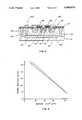
- FIG. 8is a graph showing a relationship between a dosage of an ion implantation and a Zener voltage of the semiconductor device according to the first, second and third embodiments of the present invention.
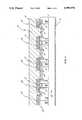
- a drain region of an N-type well 2is formed in a P-type semiconductor substrate 1.
- a P-type base 3, an N-type high impurity concentration source 10 and a P-type high impurity concentration region 11are formed in the surface portion of the N-well 2.
- a gate electrode 5is formed on the surface of the N-well 2, with a gate insulation film 6 interlaid between them.
- An N-type high impurity concentration region 13is also formed to operate as a cathode of a protective Zener diode having the base 3 as its anode.
- the base 3 and the source 10are connected together by a source electrode 8, while the drain region of the N-type well 2 and the impurity region 13 operating as the cathode of the Zener diode are connected to a drain electrode 9 through an N + impurity region 7.
- Numerals 12 and 14denote an interlayer insulator film and a field thermal oxide film, respectively.
- the P-type substrate 1has a resistivity of about 11.0 to 15.0 ⁇ cm.
- the N-type well region 2is formed by diffusion from the surface of the substrate 1.
- the well region 2is about 6 ⁇ m deep, the surface concentration thereof being 2 to 4 ⁇ 10 16 atms/cm 2 .
- the base region 3is about 2.5 ⁇ m deep, the surface concentration thereof being 5 to 8 ⁇ 10 17 atms/cm 2 .
- the threshold voltage V T of the transistoris controlled by the surface concentration of this base region 3.
- Both the source region 10 and the P-type high impurity concentration region 11are about 1.0 ⁇ m deep, the surface concentration thereof being about 1 ⁇ 10 20 atms/cm 2 .
- the N-type high impurity concentration region 7 of the drain regionis formed simultaneously with the source 10.
- the concentration of the region 13, which determines a Zener voltage,can be controlled accurately by an ion implantation method.
- the region 13is formed with an acceleration voltage of 50 keV and a dose of 2 ⁇ 10 13 cm -2 , the depth being about 2 ⁇ m, and the surface concentration being controlled to be about 1 ⁇ 10 17 atm/cm 2 .
- the gate electrode 5is 10 ⁇ m wide and spaced from one another by 15 ⁇ m.
- the dimensions of a contact holeare 10 ⁇ m on the source side and 6 ⁇ m on the drain side, while an aluminum electrode has a width of 10 ⁇ m on the drain side and of 15 ⁇ m on the source side.
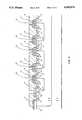
- FIG. 5is a plan view of the present embodiment. Each region corresponds to that of FIG. 4.
- the high impurity concentration region 13 for forming the Zener diodeis so formed as to surround the gate electrode 5.
- the width of about 5 to 10 ⁇ mis sufficient for this region, and the formation of this region does not need an additional device element area. This is because the Zener diode can be formed between the source and the drain by utilizing a region which is necessitated for spacing the high impurity concentration region 7 and the base region 3 by 10 ⁇ m or more so as to allow a sufficient value of current.
- numeral 15represents a drain contact region and 16 a source contact region, and other numerals correspond to those of the regions of FIG. 4, respectively.
- a drain region of an N-type epitaxial layer 62'is formed on an N-type high impurity concentration buried region 62a' buried on the P-type semiconductor substrate 61' with the epitaxial layer 62' isolated by an element isolation region 61a'.
- a drain lead-out region of an N-type high impurity concentration region 65'is formed extending from the buried layer 62a' to the surface of the epitaxial layer 62'.
- a P-type base 63', an N-type high impurity concentration source 64' and a cathode of a Zener diode of an N-type high impurity concentration regions 66'are formed on the surface of the epitaxial layer 62'.
- a gate 68'is formed on the epitaxial layer 62' with the gate insulation film between them.
- a source electrode 69s' connecting the source 64' and the base 63' together and a drain electrode 69d' connected to the impurity region 65'are provided.
- a semiconductor substrate 4'consists of an N + -type substrate 21' and an N-type drain region 22' formed on the N + -type substrate 21'.
- a drain electrode 9'is formed on the lower surface of this substrate 4', while a P-type base region 3', an N + -type source region 10', and a gate polysilicon electrode 5' and a source aluminum electrode electrode 8', are formed in the upper surface thereof.
- Numeral 12'represents an interlayer insulation film, and 11' a high-concentration P + -type base region.
- the characteristic feature of the present embodimentis that the impurity region 13' is provided, and a Zener diode is formed between a source and a drain by making the P-type base region 3' contact with an N-type impurity region 13'.
- the voltage of the Zener diodecan be controlled independent of the threshold voltage V T of the vertical field effect transistor by varying the concentration of the N-type impurity region 13'.
- An equivalent circuit of the semiconductor device of the first, second and third embodiments of the present inventionalso has a construction wherein a Zener diode D Z for protection is connected between the drain D and the source S of FET 30 as shown in FIG. 2.
- FIG. 8is a characteristic graph showing the relationship between a dose of ion implantation and a Zener voltage when an ccceleration voltage is 100 keV.
- the Zener voltagecan be set at a desired value on the basis of the relationship shown in FIG. 8.
Landscapes
- Metal-Oxide And Bipolar Metal-Oxide Semiconductor Integrated Circuits (AREA)
- Insulated Gate Type Field-Effect Transistor (AREA)
- Semiconductor Integrated Circuits (AREA)
Abstract
Description
Claims (9)
Applications Claiming Priority (2)
| Application Number | Priority Date | Filing Date | Title |
|---|---|---|---|
| JP29701187 | 1987-11-24 | ||
| JP62-297011 | 1987-11-24 |
Publications (1)
| Publication Number | Publication Date |
|---|---|
| US4990976Atrue US4990976A (en) | 1991-02-05 |
Family
ID=17841093
Family Applications (1)
| Application Number | Title | Priority Date | Filing Date |
|---|---|---|---|
| US07/274,918Expired - LifetimeUS4990976A (en) | 1987-11-24 | 1988-11-22 | Semiconductor device including a field effect transistor having a protective diode between source and drain thereof |
Country Status (3)
| Country | Link |
|---|---|
| US (1) | US4990976A (en) |
| EP (1) | EP0318297B1 (en) |
| DE (1) | DE3877533T2 (en) |
Cited By (17)
| Publication number | Priority date | Publication date | Assignee | Title |
|---|---|---|---|---|
| US5191395A (en)* | 1990-04-02 | 1993-03-02 | Fuji Electric Co., Ltd. | Mos type semiconductor device with means to prevent parasitic bipolar transistor |
| US5357393A (en)* | 1992-05-05 | 1994-10-18 | Xerox Corporation | Integrated ultra low leakage high voltage protection circuit |
| US5410275A (en)* | 1993-12-13 | 1995-04-25 | Motorola Inc. | Amplifier circuit suitable for use in a radiotelephone |
| US5416351A (en)* | 1991-10-30 | 1995-05-16 | Harris Corporation | Electrostatic discharge protection |
| US5475258A (en)* | 1992-10-30 | 1995-12-12 | Nippondenso Co., Ltd. | Power semiconductor device with protective element |
| US5616943A (en)* | 1993-09-29 | 1997-04-01 | At&T Global Information Solutions Company | Electrostatic discharge protection system for mixed voltage application specific integrated circuit design |
| US5629544A (en)* | 1995-04-25 | 1997-05-13 | International Business Machines Corporation | Semiconductor diode with silicide films and trench isolation |
| US5701071A (en)* | 1995-08-21 | 1997-12-23 | Fujitsu Limited | Systems for controlling power consumption in integrated circuits |
| US5767550A (en)* | 1996-04-12 | 1998-06-16 | National Semiconductor Corporation | Integrated zener diode overvoltage protection structures in power DMOS device applications |
| US5907174A (en)* | 1993-10-21 | 1999-05-25 | Hyundai Electronics Industries Co., Ltd. | Electrostatic discharge protecting transistor |
| US6229182B1 (en)* | 1998-06-09 | 2001-05-08 | U.S. Philips Corporation | Semiconductor device having protection against electrostatic discharge |
| US6271999B1 (en) | 1998-11-20 | 2001-08-07 | Taiwan Semiconductor Manufacturing Company | ESD protection circuit for different power supplies |
| US20020093094A1 (en)* | 2001-01-16 | 2002-07-18 | Hitachi, Ltd. | Semiconductor device |
| US20100059875A1 (en)* | 2008-09-10 | 2010-03-11 | Renesas Technology Corp. | Semiconductor device |
| US20130264645A1 (en)* | 2006-08-24 | 2013-10-10 | Infineon Technologies Ag | Diode Biased ESD Protection Device and Method |
| US20180040601A1 (en)* | 2015-04-15 | 2018-02-08 | Sharp Kabushiki Kaisha | Semiconductor device and composite semiconductor device |
| US20200105740A1 (en)* | 2018-09-28 | 2020-04-02 | Taiwan Semiconductor Manufacturing Co., Ltd. | Integrated esd enhancement circuit for soi device |
Families Citing this family (6)
| Publication number | Priority date | Publication date | Assignee | Title |
|---|---|---|---|---|
| IT1237666B (en)* | 1989-10-31 | 1993-06-15 | Sgs Thomson Microelectronics | PROCESS FOR THE MANUFACTURE OF A PROGRAMMING VOLTAGE LIMITER COMPONENT AND BUILT-IN VOLTAGE STABILIZER IN AN ELECTRIC DEVICE WITH EEPROM MEMORY CELLS |
| DE4120394A1 (en)* | 1991-06-20 | 1992-12-24 | Bosch Gmbh Robert | MONOLITHICALLY INTEGRATED CIRCUIT ARRANGEMENT |
| US5399893A (en)* | 1993-08-24 | 1995-03-21 | Motorola, Inc. | Diode protected semiconductor device |
| EP0765025A3 (en)* | 1995-09-21 | 1998-12-30 | Siemens Aktiengesellschaft | Start-up circuit and semiconductor device for such a start-up circuit |
| TW530405B (en)* | 2000-10-16 | 2003-05-01 | Koninkl Philips Electronics Nv | Integrated circuit provided with overvoltage protection and method for manufacture thereof |
| DE102004011703A1 (en)* | 2004-03-10 | 2005-09-29 | Austriamicrosystems Ag | Semiconductor device with integrated zener diode and method of manufacture |
Citations (6)
| Publication number | Priority date | Publication date | Assignee | Title |
|---|---|---|---|---|
| US4100561A (en)* | 1976-05-24 | 1978-07-11 | Rca Corp. | Protective circuit for MOS devices |
| US4145703A (en)* | 1977-04-15 | 1979-03-20 | Supertex, Inc. | High power MOS device and fabrication method therefor |
| JPS5548474A (en)* | 1978-09-29 | 1980-04-07 | Mitsubishi Electric Corp | Plasma arc welding unit |
| JPS5998557A (en)* | 1982-11-27 | 1984-06-06 | Nissan Motor Co Ltd | Mos transistor |
| JPS613469A (en)* | 1984-06-15 | 1986-01-09 | Rohm Co Ltd | bidirectional zener diode |
| JPS62102555A (en)* | 1985-10-30 | 1987-05-13 | Nissan Motor Co Ltd | Semiconductor device |
Family Cites Families (1)
| Publication number | Priority date | Publication date | Assignee | Title |
|---|---|---|---|---|
| US4712124A (en)* | 1986-12-22 | 1987-12-08 | North American Philips Corporation | Complementary lateral insulated gate rectifiers with matched "on" resistances |
- 1988
- 1988-11-22USUS07/274,918patent/US4990976A/ennot_activeExpired - Lifetime
- 1988-11-24EPEP88311152Apatent/EP0318297B1/ennot_activeExpired - Lifetime
- 1988-11-24DEDE8888311152Tpatent/DE3877533T2/ennot_activeExpired - Fee Related
Patent Citations (6)
| Publication number | Priority date | Publication date | Assignee | Title |
|---|---|---|---|---|
| US4100561A (en)* | 1976-05-24 | 1978-07-11 | Rca Corp. | Protective circuit for MOS devices |
| US4145703A (en)* | 1977-04-15 | 1979-03-20 | Supertex, Inc. | High power MOS device and fabrication method therefor |
| JPS5548474A (en)* | 1978-09-29 | 1980-04-07 | Mitsubishi Electric Corp | Plasma arc welding unit |
| JPS5998557A (en)* | 1982-11-27 | 1984-06-06 | Nissan Motor Co Ltd | Mos transistor |
| JPS613469A (en)* | 1984-06-15 | 1986-01-09 | Rohm Co Ltd | bidirectional zener diode |
| JPS62102555A (en)* | 1985-10-30 | 1987-05-13 | Nissan Motor Co Ltd | Semiconductor device |
Non-Patent Citations (2)
| Title |
|---|
| Sze "Physics of Semiconductor Dev.", pp. 494-495, (1981). |
| Sze Physics of Semiconductor Dev. , pp. 494 495, (1981).* |
Cited By (31)
| Publication number | Priority date | Publication date | Assignee | Title |
|---|---|---|---|---|
| US5191395A (en)* | 1990-04-02 | 1993-03-02 | Fuji Electric Co., Ltd. | Mos type semiconductor device with means to prevent parasitic bipolar transistor |
| US5416351A (en)* | 1991-10-30 | 1995-05-16 | Harris Corporation | Electrostatic discharge protection |
| US5357393A (en)* | 1992-05-05 | 1994-10-18 | Xerox Corporation | Integrated ultra low leakage high voltage protection circuit |
| US5475258A (en)* | 1992-10-30 | 1995-12-12 | Nippondenso Co., Ltd. | Power semiconductor device with protective element |
| US5616943A (en)* | 1993-09-29 | 1997-04-01 | At&T Global Information Solutions Company | Electrostatic discharge protection system for mixed voltage application specific integrated circuit design |
| US6515839B1 (en) | 1993-09-29 | 2003-02-04 | Hoang P. Nguyen | Electronic discharge protection system for mixed voltage application specific circuit design |
| US5907174A (en)* | 1993-10-21 | 1999-05-25 | Hyundai Electronics Industries Co., Ltd. | Electrostatic discharge protecting transistor |
| US5410275A (en)* | 1993-12-13 | 1995-04-25 | Motorola Inc. | Amplifier circuit suitable for use in a radiotelephone |
| US5477192A (en)* | 1993-12-13 | 1995-12-19 | Motorola | Amplifier suitable for use in a radiotelephone |
| US5629544A (en)* | 1995-04-25 | 1997-05-13 | International Business Machines Corporation | Semiconductor diode with silicide films and trench isolation |
| US5701071A (en)* | 1995-08-21 | 1997-12-23 | Fujitsu Limited | Systems for controlling power consumption in integrated circuits |
| US5767550A (en)* | 1996-04-12 | 1998-06-16 | National Semiconductor Corporation | Integrated zener diode overvoltage protection structures in power DMOS device applications |
| US6229182B1 (en)* | 1998-06-09 | 2001-05-08 | U.S. Philips Corporation | Semiconductor device having protection against electrostatic discharge |
| US6271999B1 (en) | 1998-11-20 | 2001-08-07 | Taiwan Semiconductor Manufacturing Company | ESD protection circuit for different power supplies |
| US6400542B1 (en) | 1998-11-20 | 2002-06-04 | Taiwan Semiconductor Manufacturing Company | ESD protection circuit for different power supplies |
| US6426855B2 (en) | 1998-11-20 | 2002-07-30 | Taiwan Semiconductor Manufacturing Company | ESD protection circuit for different power supplies |
| US20020093094A1 (en)* | 2001-01-16 | 2002-07-18 | Hitachi, Ltd. | Semiconductor device |
| US20040135248A1 (en)* | 2001-01-16 | 2004-07-15 | Renesas Technology Corporation | Semiconductor device |
| US6842346B2 (en) | 2001-01-16 | 2005-01-11 | Renesas Technology Corp. | Semiconductor device |
| US6700793B2 (en)* | 2001-01-16 | 2004-03-02 | Renesas Technology Corporation | Semiconductor device |
| US9263428B2 (en)* | 2006-08-24 | 2016-02-16 | Infineon Technologies Ag | Diode biased ESD protection device and method |
| US9859270B2 (en) | 2006-08-24 | 2018-01-02 | Infineon Technologies Ag | Diode biased ESD protection devices and methods |
| US20130264645A1 (en)* | 2006-08-24 | 2013-10-10 | Infineon Technologies Ag | Diode Biased ESD Protection Device and Method |
| US20130264646A1 (en)* | 2006-08-24 | 2013-10-10 | Infineon Technologies Ag | Diode Biased ESD Protection Device and Method |
| US9129805B2 (en)* | 2006-08-24 | 2015-09-08 | Infineon Technologies Ag | Diode biased ESD protection device and method |
| US20100059875A1 (en)* | 2008-09-10 | 2010-03-11 | Renesas Technology Corp. | Semiconductor device |
| US9478483B2 (en) | 2008-09-10 | 2016-10-25 | Renesas Electronics Corporation | Semiconductor device having a chip mounting portion on which a separated plated layer is disposed |
| US8040708B2 (en)* | 2008-09-10 | 2011-10-18 | Renesas Electronics Corporation | Semiconductor device |
| US20180040601A1 (en)* | 2015-04-15 | 2018-02-08 | Sharp Kabushiki Kaisha | Semiconductor device and composite semiconductor device |
| US20200105740A1 (en)* | 2018-09-28 | 2020-04-02 | Taiwan Semiconductor Manufacturing Co., Ltd. | Integrated esd enhancement circuit for soi device |
| US10867988B2 (en)* | 2018-09-28 | 2020-12-15 | Taiwan Semiconductor Manufacturing Co., Ltd. | Integrated ESD enhancement circuit for SOI device |
Also Published As
| Publication number | Publication date |
|---|---|
| EP0318297A2 (en) | 1989-05-31 |
| EP0318297B1 (en) | 1993-01-13 |
| DE3877533T2 (en) | 1993-06-09 |
| DE3877533D1 (en) | 1993-02-25 |
| EP0318297A3 (en) | 1989-07-26 |
Similar Documents
| Publication | Publication Date | Title |
|---|---|---|
| US4990976A (en) | Semiconductor device including a field effect transistor having a protective diode between source and drain thereof | |
| US5998836A (en) | Trench-gated power MOSFET with protective diode | |
| US6072215A (en) | Semiconductor device including lateral MOS element | |
| US5920087A (en) | Lateral IGBT | |
| US5283201A (en) | High density power device fabrication process | |
| US6140678A (en) | Trench-gated power MOSFET with protective diode | |
| US5016066A (en) | Vertical power MOSFET having high withstand voltage and high switching speed | |
| US6642599B1 (en) | Semiconductor device and method of manufacturing the same | |
| JP2968222B2 (en) | Semiconductor device and method for preparing silicon wafer | |
| US6884683B2 (en) | Trench DMOS transistor having a zener diode for protection from electro-static discharge | |
| EP0484321B1 (en) | Method of fabricating insulated gate semiconductor device | |
| US20030207538A1 (en) | Trench DMOS transistor with embedded trench schottky rectifier | |
| US20020055232A1 (en) | Method of operation of punch-through field effect transistor | |
| US5191395A (en) | Mos type semiconductor device with means to prevent parasitic bipolar transistor | |
| US5686750A (en) | Power semiconductor device having improved reverse recovery voltage | |
| JP2007318158A (en) | Lateral MOS field effect transistor having a lightly doped drain and method of manufacturing the same | |
| JPH0336311B2 (en) | ||
| US5545915A (en) | Semiconductor device having field limiting ring and a process therefor | |
| KR20060040592A (en) | Semiconductor device having edge termination structure and method for forming same | |
| JPH0817233B2 (en) | Insulated gate bipolar transistor | |
| US7276772B2 (en) | Semiconductor device | |
| US5410171A (en) | Vertical type semiconductor with main current section and emulation current section | |
| US5156992A (en) | Process for forming poly-sheet pillar transistor DRAM cell | |
| JP2000077663A (en) | Field effect type semiconductor device | |
| EP0193172A2 (en) | Vertical MOS transistor with peripheral circuit |
Legal Events
| Date | Code | Title | Description |
|---|---|---|---|
| AS | Assignment | Owner name:NEC CORPORATION, 33-1, SHIBA 5-CHOME, MINATO-KU, T Free format text:ASSIGNMENT OF ASSIGNORS INTEREST.;ASSIGNOR:HATTORI, MASAYUKI;REEL/FRAME:004971/0320 Effective date:19881118 Owner name:NEC CORPORATION, JAPAN Free format text:ASSIGNMENT OF ASSIGNORS INTEREST;ASSIGNOR:HATTORI, MASAYUKI;REEL/FRAME:004971/0320 Effective date:19881118 | |
| STCF | Information on status: patent grant | Free format text:PATENTED CASE | |
| FEPP | Fee payment procedure | Free format text:PAYOR NUMBER ASSIGNED (ORIGINAL EVENT CODE: ASPN); ENTITY STATUS OF PATENT OWNER: LARGE ENTITY | |
| FPAY | Fee payment | Year of fee payment:4 | |
| FEPP | Fee payment procedure | Free format text:PAYOR NUMBER ASSIGNED (ORIGINAL EVENT CODE: ASPN); ENTITY STATUS OF PATENT OWNER: LARGE ENTITY | |
| REMI | Maintenance fee reminder mailed | ||
| FPAY | Fee payment | Year of fee payment:8 | |
| SULP | Surcharge for late payment | ||
| FPAY | Fee payment | Year of fee payment:12 | |
| AS | Assignment | Owner name:NEC ELECTRONICS CORPORATION, JAPAN Free format text:ASSIGNMENT OF ASSIGNORS INTEREST;ASSIGNOR:NEC CORPORATION;REEL/FRAME:013758/0440 Effective date:20021101 |