US4989985A - Densitometer for measuring specular reflectivity - Google Patents
Densitometer for measuring specular reflectivityDownload PDFInfo
- Publication number
- US4989985A US4989985AUS07/246,242US24624288AUS4989985AUS 4989985 AUS4989985 AUS 4989985AUS 24624288 AUS24624288 AUS 24624288AUS 4989985 AUS4989985 AUS 4989985A
- Authority
- US
- United States
- Prior art keywords
- light rays
- densitometer
- photosensor
- collector lens
- light
- Prior art date
- Legal status (The legal status is an assumption and is not a legal conclusion. Google has not performed a legal analysis and makes no representation as to the accuracy of the status listed.)
- Expired - Lifetime
Links
- 238000002310reflectometryMethods0.000titleclaimsabstractdescription27
- 239000002245particleSubstances0.000claimsabstractdescription67
- 230000004907fluxEffects0.000claimsabstractdescription23
- 230000009467reductionEffects0.000claimsabstractdescription5
- 238000012360testing methodMethods0.000description15
- 239000000463materialSubstances0.000description12
- 238000011161developmentMethods0.000description10
- 230000018109developmental processEffects0.000description10
- 108091008695photoreceptorsProteins0.000description9
- 230000032258transportEffects0.000description8
- 239000000843powderSubstances0.000description7
- 238000012546transferMethods0.000description7
- 239000008187granular materialSubstances0.000description5
- 230000005291magnetic effectEffects0.000description5
- 230000000875corresponding effectEffects0.000description4
- 238000000034methodMethods0.000description4
- 239000000203mixtureSubstances0.000description4
- 230000008569processEffects0.000description4
- 238000012986modificationMethods0.000description3
- 230000004048modificationEffects0.000description3
- 238000012545processingMethods0.000description3
- 230000032683agingEffects0.000description2
- 238000004140cleaningMethods0.000description2
- 238000010586diagramMethods0.000description2
- 230000007246mechanismEffects0.000description2
- 230000003287optical effectEffects0.000description2
- 230000003134recirculating effectEffects0.000description2
- 238000000926separation methodMethods0.000description2
- 238000001228spectrumMethods0.000description2
- 229920002799BoPETPolymers0.000description1
- 239000005041Mylar™Substances0.000description1
- BUGBHKTXTAQXES-UHFFFAOYSA-NSeleniumChemical compound[Se]BUGBHKTXTAQXES-UHFFFAOYSA-N0.000description1
- RTAQQCXQSZGOHL-UHFFFAOYSA-NTitaniumChemical compound[Ti]RTAQQCXQSZGOHL-UHFFFAOYSA-N0.000description1
- NIXOWILDQLNWCW-UHFFFAOYSA-Nacrylic acid groupChemical groupC(C=C)(=O)ONIXOWILDQLNWCW-UHFFFAOYSA-N0.000description1
- 238000013459approachMethods0.000description1
- 239000003086colorantSubstances0.000description1
- 230000002596correlated effectEffects0.000description1
- 230000007423decreaseEffects0.000description1
- 238000001739density measurementMethods0.000description1
- 230000000694effectsEffects0.000description1
- 230000005294ferromagnetic effectEffects0.000description1
- 238000005286illuminationMethods0.000description1
- 230000006872improvementEffects0.000description1
- 150000002500ionsChemical class0.000description1
- 238000005259measurementMethods0.000description1
- 229920000515polycarbonatePolymers0.000description1
- 239000004417polycarbonateSubstances0.000description1
- 229910052711seleniumInorganic materials0.000description1
- 239000011669seleniumSubstances0.000description1
- 150000003384small moleculesChemical class0.000description1
- 230000003595spectral effectEffects0.000description1
- 239000007921spraySubstances0.000description1
- 229920001169thermoplasticPolymers0.000description1
- 239000004416thermosoftening plasticSubstances0.000description1
- 229910052719titaniumInorganic materials0.000description1
- 239000010936titaniumSubstances0.000description1
- 239000012780transparent materialSubstances0.000description1
Images


Classifications
- G—PHYSICS
- G01—MEASURING; TESTING
- G01N—INVESTIGATING OR ANALYSING MATERIALS BY DETERMINING THEIR CHEMICAL OR PHYSICAL PROPERTIES
- G01N21/00—Investigating or analysing materials by the use of optical means, i.e. using sub-millimetre waves, infrared, visible or ultraviolet light
- G01N21/17—Systems in which incident light is modified in accordance with the properties of the material investigated
- G01N21/55—Specular reflectivity
- G—PHYSICS
- G03—PHOTOGRAPHY; CINEMATOGRAPHY; ANALOGOUS TECHNIQUES USING WAVES OTHER THAN OPTICAL WAVES; ELECTROGRAPHY; HOLOGRAPHY
- G03G—ELECTROGRAPHY; ELECTROPHOTOGRAPHY; MAGNETOGRAPHY
- G03G15/00—Apparatus for electrographic processes using a charge pattern
- G03G15/06—Apparatus for electrographic processes using a charge pattern for developing
- G03G15/08—Apparatus for electrographic processes using a charge pattern for developing using a solid developer, e.g. powder developer
- G03G15/0822—Arrangements for preparing, mixing, supplying or dispensing developer
- G03G15/0848—Arrangements for testing or measuring developer properties or quality, e.g. charge, size, flowability
- G03G15/0849—Detection or control means for the developer concentration
- G03G15/0855—Detection or control means for the developer concentration the concentration being measured by optical means
- G—PHYSICS
- G01—MEASURING; TESTING
- G01N—INVESTIGATING OR ANALYSING MATERIALS BY DETERMINING THEIR CHEMICAL OR PHYSICAL PROPERTIES
- G01N21/00—Investigating or analysing materials by the use of optical means, i.e. using sub-millimetre waves, infrared, visible or ultraviolet light
- G01N21/17—Systems in which incident light is modified in accordance with the properties of the material investigated
- G01N21/55—Specular reflectivity
- G01N2021/559—Determining variation of specular reflection within diffusively reflecting sample
- G—PHYSICS
- G01—MEASURING; TESTING
- G01N—INVESTIGATING OR ANALYSING MATERIALS BY DETERMINING THEIR CHEMICAL OR PHYSICAL PROPERTIES
- G01N21/00—Investigating or analysing materials by the use of optical means, i.e. using sub-millimetre waves, infrared, visible or ultraviolet light
- G01N21/17—Systems in which incident light is modified in accordance with the properties of the material investigated
- G01N21/59—Transmissivity
- G01N21/5907—Densitometers
- G01N2021/5957—Densitometers using an image detector type detector, e.g. CCD
- G—PHYSICS
- G01—MEASURING; TESTING
- G01N—INVESTIGATING OR ANALYSING MATERIALS BY DETERMINING THEIR CHEMICAL OR PHYSICAL PROPERTIES
- G01N21/00—Investigating or analysing materials by the use of optical means, i.e. using sub-millimetre waves, infrared, visible or ultraviolet light
- G01N21/17—Systems in which incident light is modified in accordance with the properties of the material investigated
- G01N21/25—Colour; Spectral properties, i.e. comparison of effect of material on the light at two or more different wavelengths or wavelength bands
- G01N21/31—Investigating relative effect of material at wavelengths characteristic of specific elements or molecules, e.g. atomic absorption spectrometry
- G01N21/35—Investigating relative effect of material at wavelengths characteristic of specific elements or molecules, e.g. atomic absorption spectrometry using infrared light
- G01N21/359—Investigating relative effect of material at wavelengths characteristic of specific elements or molecules, e.g. atomic absorption spectrometry using infrared light using near infrared light
- G—PHYSICS
- G01—MEASURING; TESTING
- G01N—INVESTIGATING OR ANALYSING MATERIALS BY DETERMINING THEIR CHEMICAL OR PHYSICAL PROPERTIES
- G01N2201/00—Features of devices classified in G01N21/00
- G01N2201/06—Illumination; Optics
- G01N2201/062—LED's
- G01N2201/0621—Supply
- G—PHYSICS
- G03—PHOTOGRAPHY; CINEMATOGRAPHY; ANALOGOUS TECHNIQUES USING WAVES OTHER THAN OPTICAL WAVES; ELECTROGRAPHY; HOLOGRAPHY
- G03G—ELECTROGRAPHY; ELECTROPHOTOGRAPHY; MAGNETOGRAPHY
- G03G15/00—Apparatus for electrographic processes using a charge pattern
- G03G15/50—Machine control of apparatus for electrographic processes using a charge pattern, e.g. regulating differents parts of the machine, multimode copiers, microprocessor control
- G03G15/5033—Machine control of apparatus for electrographic processes using a charge pattern, e.g. regulating differents parts of the machine, multimode copiers, microprocessor control by measuring the photoconductor characteristics, e.g. temperature, or the characteristics of an image on the photoconductor
- G03G15/5041—Detecting a toner image, e.g. density, toner coverage, using a test patch
Definitions
- This inventionrelates generally to an electrophotographic printing machine, and more particularly concerns an improved infrared densitometer for use therein to detect a reduction in the specular reflectivity as toner particles are progressively deposited on a photoconductive member.
- the photoconductive memberis charged to a substantially uniform potential to sensitize the surface thereof.
- the charged portion of the photoconductive memberis exposed to a light image of an original document being reproduced. Exposure of the charged photoconductive member selectively dissipates the charge thereon in the irradiated areas.
- the latent imageis developed by bringing marking or toner particles into contact therewith. This forms a powder image on the photoconductive member which is subsequently transferred to a copy sheet.
- the copy sheetis heated to permanently affix the marking particles thereto in image configuration.
- Typical two component developer mixes employedare well known in the art, and generally comprise dyed or colored thermoplastic powders, known in the art as toner particles, which are mixed with coarser carrier granules, such as ferromagnetic granules.
- the toner particles and carrier granulesare selected such that the toner particles acquire the appropriate charge relative to the electrostatic latent image recorded on the photoconductive surface.
- the developer mixis brought into contact with the charged photoconductive surface the greater attractive force of the electrostatic latent image recorded thereon causes the toner particles to transfer from the carrier granules and adhere to the electrostatic latent image.
- Multi-color electrophotographic printingis substantially identical to the foregoing process of black and white printing. However, rather than forming a single latent image on the photoconductive surface, successive latent images corresponding to different colors are recorded thereon. Each single color electrostatic latent image is developed with toner particles of a color complimentary thereto. This process is repeated a plurality of cycles for differently colored images and their respective complimentarily colored toner particles. For example, a red filtered light image is developed with cyan toner particles, while a green filtered light image is developed with magenta toner particles and a blue filtered light image with yellow toner particles. Each single color toner powder image is transferred to the copy sheet in superimposed registration with the prior toner powder image.
- An illustrative electrophotographic printing machine for producing color copiesis the Model No. 1005 made by the Xerox Corporation.
- densitometersfor measuring the optical density of black toner particles is well known. However, densitometers used for black toner particles are generally unsuitable for use with colored toner particles. Densitometers of this type are generally sensitive to the large component of diffusely reflected flux in the infrared from colored toner particles which gives false density measurements. There do not appear to be any comparable densitometers for measuring the density of colored toner particles. Various approaches have been used to measure density. The following disclosures appear to be relevant.
- US-A-4,054,391discloses a specular reflectance micordensitometer wherein the amount of light specularly reflected by a test surface is correlated to the density of particle coverage on the surface.
- Light incident on the test surface from an illuminating microscopespecularly reflects into a collecting microscope and is compared to the light reflected from a clean test surface.
- the reflectance of a clean photoreceptor surface and a toned photoreceptor surfaceis measured and the ratio determined.
- US-A-4,284,356describes light sources and light detectors for illuminating and comparing surface reflectivity. First and second reflects light beams are compared to determine the greater reflectivity of the first and second respective sheet surfaces.
- the light beams from the light sourcemay be either collimated light beams or non-collimated (diffuse) light beams.
- the light detectorshave an electrical output signal responsive to the intensity or density of the light beams incident thereon.
- US-A-4,553,033discloses an infrared reflectance densitometer including a light emitting diode, a collimating lens through which light is projected to a photosensitive surface, a collector lens and a field lens through which reflected light is focused onto a signal photodiode, and a control photodiode onto which a portion of reflected light is directed to control light output.
- the mount of light received on the signal photodiodeis a measurement of the reflectance from the surface of the photoreceptor which, in turn, is proportional to the density of the toner particles thereon.
- an apparatus for measuring the reduction in the specular reflectance of particles deposited on a surfaceincludes means for projecting light rays onto the particles on the surface. Means are provided for detecting the total reflectivity of at least the particles and the diffuse component of the total reflectivity of at least the particles and generating a total signal indicative of the total reflectivity of at least the particles and a diffuse signal indicative of the diffuse component of the total reflectivity of at least the particles. Means, responsive to the difference between the total signal and the diffuse signal, generate a specular signal indicative of the specular component of the total reflectivity of at least the particles.
- an electrophotographic printing machineof the type in which the density of marking particles deposited on a moving photoconductive member is detected.
- the improvementincludes means for projecting light rays onto the marking particles on the moving photoconductive member.
- Meansare provided for detecting the total reflectivity of at least the marking particles and the diffuse component of the total reflectivity of at least the marking particles and generating a total signal indicative of the total reflectivity of at least the marking particles and a diffuse signal indicative of the diffuse component of the total reflectivity of at least the marking particles.
- Meansresponsive to the difference between the total signal and the diffuse signal, generate a specular signal indicative of the specular component of the total reflectivity of at least the marking particles.
- the densitometerincludes a collimating lens and a light source positioned to project light rays though the collimating lens onto the marking particles deposited on the moving photoconductive belt.
- a collector lensis positioned to receive the light rays reflected from at least the marking particles deposited on the moving photoconductive belt.
- a photosensor arrayis positioned to receive the light rays transmitted through the collector lens. The photosensor array generates a total signal proportional to the total reflectivity of at least the marking particles and a diffuse signal proportional to the diffuse component of the total reflectivity of at least the marking particles.
- Control circuitryelectrically connected to the photosensor array, compares the total signal and the diffuse signal to determine the difference therebetween for generating a specular signal proportional to the specular component of the total reflectivity of at least the marking particles.
- Still another aspect of the present inventionis a densitometer which includes a collimating lens.
- a light sourceis positioned to project light rays through the collimating lens.
- a collector lensis positioned to receive reflected light rays.
- a photosensor arrayis positioned to receive the reflected light rays transmitted through the collector lens.
- the photosensor arrayis adapted to generate a total signal proportional to the total flux of the light rays transmitted through the collector lens and a diffuse signal proportional to the diffuse component of the total flux of the light rays transmitted through the collector lens.
- Control circuitryelectrically connected to the photosensor array, compares the total signal and the diffuse signal to determine the difference therebetween for generating a specular signal proportional to the specular component of the total flux of the light rays transmitted through the collector lens.
- FIG. 1is a schematic elevational view depicting an electrophotographic printing machine incorporating the infrared densitometer of the present invention therein;
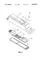
- FIG. 2is a schematic perspective view showing the densitometer used in the FIG. 1 printing machine
- FIG. 3is a fragmentary, sectional elevational view of the FIG. 2 densitometer
- FIG. 4is an enlarged plan view of the photodiode array used in the FIG. 3 densitometer.
- FIG. 5is a block diagram of the control logic associated with the FIG. 3 densitometer.
- FIG. 1schematically depicts the various components of an illustrative electrophotographic printing machine incorporating the infrared densitometer of the present invention therein. It will become evident from the following discussion that the densitometer of the present invention is equally well suited for use in a wide variety of electrostatographic printing machines, and is not necessarily limited in its application to the particular electrophotographic printing machine shown herein.
- the electrophotographic printing machineemploys a photoreceptor, i.e. a photoconductive belt 10.
- the photoconductive belt 10is made from a photoconductive material coated on a grounding layer, which, in turn, is coated on an anti-curl backing layer.
- the photoconductive materialis made from a transport layer coated on a generator layer.
- the transport layertransports positive charges from the generator layer.
- the interface layeris coated on the grounding layer.
- the transport layercontains small molecules of di-m-tolydihenylbiphenyldiamine dispersed in a polycarbonate.
- the generation layeris made from trigonal selenium.
- the grounding layeris made form a titanium coated Mylar.
- the grounding layeris very thin and allows light to pass therethrough.
- Other suitable photoconductive materials, grounding layers, and anti-curl backing layersmay also be employed.
- Belt 10moves in the direction of arrow 12 to advance successive portions of the photoconductive surface sequentially through the various processing stations disposed about the path of movement thereof.
- Belt 10is entrained about idler roller 14 and drive roller 16.
- Idler roller 14is mounted rotatably so as to rotate with belt 10.
- Drive roller 16is rotated by a motor coupled thereto by suitable means such as a belt drive. As roller 16 rotates, it advances belt 10 in the direction of arrow 12.
- corona generating devices 18 and 20charge photoconductive belt 10 to a relatively high, substantially uniform potential.
- Corona generating device 18places all of the required charge on photoconductive belt 10.
- Corona generating device 20acts as a leveling device, and fills in any areas missed by corona generating device 18.
- Exposure station Bincludes a moving lens system, generally designated by the reference number 22, and a color filter mechanism, shown generally by the reference numeral 24.
- An original document 26is supported stationarily upon a transparent viewing platen 28. Successive incremental areas of the original document are illuminated by means of a moving lamp assembly, shown generally by the reference numeral 30.
- Mirrors 32, 34 and 36reflect the light rays through lens 22.
- Lens 22is adapted to scan successive areas of illumination of platen 28. The light rays from lens 22 are reflected by mirrors 38, 40, and 42 to be focused on the charged portion of photoconductive belt 10.
- Lamp assembly 30, mirrors 32, 34 and 36, lens 22, and filter 24are moved in a timed relationship with respect to the movement of photoconductive belt 10 to produce a flowing light image of the original document on photoconductive belt 10 in a non-distorted manner.
- filter mechanism 24interposes selected color filters into the optical light path of lens 22.
- the color filtersoperate on the light rays passing through the lens to record an electrostatic latent image, i.e. a latent electrostatic charge pattern, on the photoconductive belt corresponding to a specific color of the flowing light image of the original document.
- Exposure station Balso includes a test area generator, indicated generally by the reference numeral 43, comprising a light source to project a test light image onto the charged portion of the photoconductive surface in the inter-image region, i.e. the region between successive electrostatic latent images recorded on photoconductive belt 10, to record a test area.
- the test area, as well as the electrostatic latent image recorded on the photoconductive surface of belt 10are developed with toner particles at the development stations.
- Development station Cincludes four individual developer units generally indicated by the reference numerals 44, 46, 48 and 50.
- the developer unitsare of a type generally referred to in the art as "magnetic brush development units.”
- a magnetic brush development systememploys a magnetizable developer material including magnetic carrier granules having toner particles adhering triboelectrically thereto.
- the developer materialis continually brought through a directional flux field to form a brush of developer material.
- the developer particlesare continually moving so as to provide the brush consistently with fresh developer material. Development is achieved by bringing the brush of developer material into contact with the photoconductive surface.
- Developer units 44, 46 and 48apply toner particles of a specific color which corresponds to the compliment of the specific color separated electrostatic latent image recorded on the photoconductive surface.
- the color of each of the toner particlesis adapted to absorb light within a preselected spectral region of the electromagnetic wave spectrum corresponding to the wave length of light transmitted through the filter. For example, an electrostatic latent image formed by passing the light image through a green filter will record the red and blue portions of the spectrums as areas of relatively high charge density on photoconductive belt 10, while the green light rays will pass through the filter and cause the charge density on the photoconductive belt 10 to be reduced to a voltage level ineffective for development.
- developer unit 44applies green absorbing (magenta) toner particles onto the electrostatic latent image recorded on photoconductive belt 10.
- a blue separationis developed by developer unit 46 with blue absorbing (yellow) toner particles, while the red separation is developed by developer unit 48 with red absorbing (cyan) toner particles.
- Developer unit 50contains black toner particles and may be used to develop the electrostatic latent image formed from a black and white original document.
- Each of the developer unitsis moved into and out of the operative position. In the operative position, the magnetic brush is closely adjacent the photoconductive belt, while, in the non-operative position, the magnetic brush is spaced therefrom.
- each electrostatic latent imageonly one developer unit is in the operative position, the remaining developer units are in the non-operative position. This insures that each electrostatic latent image and successive test areas are developed with toner particles of the appropriate color without co-mingling.
- developer unit 44is shown in the operative position with developer units 46, 48 and 50 being in the non-operative position.
- the developed test areapasses beneath an infrared densitometer, indicated generally by the reference number 51.
- Infrared densitometer 51is positioned adjacent the photoconductive surface of belt 10 to generate electrical signals proportional to the developed toner mass of the test area. The detailed structure of densitometer 51 will be described hereinafter with reference to FIGS. 2 through 5, inclusive.
- the toner imageis moved to transfer station D where the toner image is transferred to a sheet of support material 52, such as plain paper amongst others.
- the sheet transport apparatusindicated generally by the reference numeral 54, moves sheet 52 into contact with photoconductive belt 10.
- Sheet transport 54has a pair of spaced belts 56 entrained about three rolls 58, 60 and 62.
- a gripper 64extends between belts 56 and moves in unison therewith.
- Sheet 52is advanced from a stack of sheets 72 disposed on ray 74.
- Feed roll 77advances the uppermost sheet from stack 72 into the nip defined by forwarding rollers 76 and 78. Forwarding rollers 76 and 78 advance sheet 52 to sheet transport 54.
- Sheet 52is advanced by forwarding rollers 76 and 78 in synchronism with the movement of gripper 64. In this way, the leading edge of sheet 52 arrives at a preselected position to be received by the open gripper 64. The gripper then closes securing the sheet thereto for movement therewith in a recirculating path. The leading edge of the sheet is secured releasably by gripper 64. As the belts move in the direction of arrow 66, the sheet 52 moves into contact with the photoconductive belt, in synchronism with the toner image developed thereon, at the transfer zone 68.
- a corona generating device 70sprays ions onto the backside of the sheet so as to charge the sheet to the proper magnitude and polarity for attracting the toner image from photoconductive belt 10 thereto.
- Sheet 52remains secured to gripper 64 so as to move in a recirculating path for three cycles. In this way, three different color toner images are transferred to sheet 52 in superimposed registration with one another.
- the aforementioned steps of charging, exposing, developing, and transferringare repeated a plurality of cycles to form a multi-color copy of a colored original document.
- Conveyor 80transports sheet 52, in the direction of arrow 82, to fusing station E where the transferred image is permanently fused to sheet 52.
- Fusing station Eincludes a heated fuser roll 84 and a pressure roll 86.
- Sheet 52passes through the nip defined by fuser roll 84 and pressure roll 86.
- the toner imagecontacts fuser roll 84 so as to be affixed to sheet 52.
- sheet 52is advanced by forwarding roll pairs 88 to catch tray 90 for subsequent removal therefrom by the machine operator.
- the last processing station in the direction of movement of belt 10, as indicated by arrow 12is cleaning station F.
- a rotatably mounted fibrous brush 92is positioned in cleaning station F and maintained in contact with photoconductive belt 10 to remove residual toner particles remaining after the transfer operation.
- lamp 94illuminates photoconductive belt 10 to remove any residual charge remaining thereon prior to the start of the next successive cycle.
- Densitometer 51includes a generally rectangularly shaped molded housing 96 made preferably from an acrylic material or any other suitable optically transparent material. Housing 96 defines a chamber 97. A cover 98 encloses the bottom of housing 96. A printed circuit writing board 100 is mounted between cover 98 and housing 96 in chamber 97. Printed circuit board 100 supports a suitable light emitting diode (LED) 102 for providing light rays to illuminate the marking particles adhering to the photoconductive surface of belt 10. A control photodiode 104 and a photodiode array 106 are also mounted on printed circuit board 100.
- LEDlight emitting diode
- photodiode array 106The details of photodiode array 106 will be described hereinafter with reference to FIG. 4.
- Connector 108is also mounted on printed circuit board 100.
- An integrated circuit chipindicated generally by the reference numeral 107, is electrically connected to LED 102, photodiode 104 and photodiode array 106 to provide drive current to LED 102 and to process the signals from photodiode 104 and photodiode array 106.
- the top surface 110 of housing 96defines a V-shaped recess, generally indicated by the reference numeral 112.
- One surface of the V-shaped recess 112supports a condenser lens 116 which is an integral collimating lens.
- the other surface of the V-shaped recess 112supports another condenser lens 114 which is an integral collector lens.
- LED 102generates near infrared light rays which are transmitted through an aperture 118 in cavity 120 onto condenser lens 116.
- Condenser lens 116collimates the light rays and focuses the light rays onto the marking or toner particles deposited on the test area recorded on the photoconductive surface of belt 10.
- Photodiode 104is positioned to receive a portion of the LED radiant flux reflected from the walls of cavity 120. The output signal from photodiode 104 is compared with a reference signal and the resultant error signal used to regulate the input current to LED 102 to compensate for LED aging and thermal effects.
- the light rays reflected from the toner particlesare collected by condenser lens 114 and directed onto the surface of photodiode array 106.
- the specular component of the reflected light rays or fluxis focused on a small spot on surface of the central segment of photodiode array 106.
- the diffuse components of the reflected light rays or fluxas shown by arrows 124, flood the entire surface of photodiode array 106. Further details of the structure of the densitometer, exclusive of photodiode array 106, may be found in U.S. Pat. No. 4,553,033 issued to Hubble, III et al. on Nov. 12, 1985, the relevant portions thereof being hereby incorporated into the present application.
- photodiode array 106is about 5 millimeter square.
- Photodiode array 106receives the light rays transmitted through condenser lens 116. These light rays are reflected from the toner particles adhering to the photoconductive surface of belt 10 and the exposed portion of the photoconductive surface of belt 10.
- a central photodiode 126receives the total reflected light rays or flux. The total reflected light rays or flux includes the specular component and the diffuse component of the reflected light rays or flux. Thus, central photodiode 126 generates an electrical signal proportional to the total reflected flux including the diffuse component and the specular component thereof.
- central photodiode 126is preferably substantially elliptical.
- Edge photodiodes 128 and 130are configured to compliment central photodiode 126 to complete photodiode array 106 which is substantially square in shape.
- Edge photodiodes 128 and 130are substantially identical to one another, being shaped as mirror images of one another.
- Edge photodiodes 128 and 130are positioned to receive only the diffuse component of the reflected light rays or flux transmitted through condenser lens 116. Hence, the electrical signal generated by edge photodiodes 128 and 130 is proportional to only the diffuse component of the reflected light rays or flux.
- FIG. 5A block diagram reflecting the integrated circuit 107 used to measure the specular component of the light rays is shown in FIG. 5.
- central photodiode 126generates an electrical signal proportional to the the sum of the specular and diffuse components of the light rays.
- Central photodiode 126is electrically connected to difference amplifier 132.
- the electrical output signals from photodiodes 128 and 130are proportional to the diffuse component of the light rays.
- Photodiodes 128 and 130are electrically connected to difference amplifier 132.
- the electrical signals from photodiodes 128 and 130are combined and transmitted to difference amplifier 132.
- the voltage output, V out , from difference amplifier 132may be expressed as:
- G 1 and G 2are gains of difference amplifier 132;
- i sis the specular component of the current output from central photodiode 126;
- i dis the diffuse component of the current output from central photodiode 126.
- i d'is the diffuse components of the combined current output from edge photodiodes 128 and 130.
- G 1 and G 2are set such that
- the voltage output from difference amplifier 132is proportional only to the specular component of the current output. This voltage output provides a measure of the area coverage of colored toner particles deposited on the photoconductive surface. This may be seen more clearly from the following Table which provides the approximate reflective properties of selected photoreceptor and toner materials at 880 nanometers incident wavelength.
- the specular reflectivityis zero and the output from difference amplifier 132 will be zero.
- the outputwill correspond to the specular reflectivity of the photoreceptor whose specular reflectivity is non-zero.
- the electrical signal from control photodiode 104is transmitted through suitable circuitry to generate a voltage output which regulates a current source 134.
- the current sourceenergizes LED 102.
- a feedback loopis formed for driving LED 102 to provide a relatively constant output.
- the output from current source 134is suitably adjusted to maintain a relatively constant light output from the LED 102.
- the densitometer of the present inventiondetects the total and diffuse components of the reflectivity of the light rays. The difference is obtained and a signal generated proportional to the specular component of the reflectivity of the light rays generated. In this way, the densitometer is capable of sensing the presence or absence of both colored or black toner particles on a photoreceptor surface.
Landscapes
- Physics & Mathematics (AREA)
- General Physics & Mathematics (AREA)
- Biochemistry (AREA)
- Life Sciences & Earth Sciences (AREA)
- Chemical & Material Sciences (AREA)
- Analytical Chemistry (AREA)
- Health & Medical Sciences (AREA)
- General Health & Medical Sciences (AREA)
- Immunology (AREA)
- Pathology (AREA)
- Control Or Security For Electrophotography (AREA)
- Investigating Or Analysing Materials By Optical Means (AREA)
- Dry Development In Electrophotography (AREA)
- Color Electrophotography (AREA)
Abstract
Description
______________________________________ U.S. Pat. No. 4,054,391 Patentee: Witte Issued: October 18, 1977 U.S. Pat. No. 4,284,356 Patentee: Heilman Issued: August 18, 1981 U.S. Pat. No. 4,553,033 Patentee: Hubble, III et al. Issued: November 12, 1985 ______________________________________
V.sub.out =G.sub.1 (i.sub.s +i.sub.d)-G.sub.2 (i.sub.d')
G.sub.1 (i.sub.d)=G.sub.2 (i.sub.d').
V.sub.out =G.sub.1 (i.sub.s).
______________________________________ SPECULAR DIFFUSE SURFACE REFLECTIVITY REFLECTIVITY ______________________________________ Photoreceptor 5-16% 12-26% Yellow Toner 0% 60% Magenta Toner 0% 64% Cyan Toner 0% 44% Black Toner 0% 1% ______________________________________
Claims (6)
Priority Applications (4)
| Application Number | Priority Date | Filing Date | Title |
|---|---|---|---|
| US07/246,242US4989985A (en) | 1988-09-19 | 1988-09-19 | Densitometer for measuring specular reflectivity |
| EP89309255AEP0360484B1 (en) | 1988-09-19 | 1989-09-12 | Densitometer for measuring specular reflectivity |
| JP1236809AJP3043766B2 (en) | 1988-09-19 | 1989-09-12 | Density meter for specular reflectance measurement |
| DE68923236TDE68923236T2 (en) | 1988-09-19 | 1989-09-12 | Densitometer for measuring specular reflectance. |
Applications Claiming Priority (1)
| Application Number | Priority Date | Filing Date | Title |
|---|---|---|---|
| US07/246,242US4989985A (en) | 1988-09-19 | 1988-09-19 | Densitometer for measuring specular reflectivity |
Publications (1)
| Publication Number | Publication Date |
|---|---|
| US4989985Atrue US4989985A (en) | 1991-02-05 |
Family
ID=22929874
Family Applications (1)
| Application Number | Title | Priority Date | Filing Date |
|---|---|---|---|
| US07/246,242Expired - LifetimeUS4989985A (en) | 1988-09-19 | 1988-09-19 | Densitometer for measuring specular reflectivity |
Country Status (4)
| Country | Link |
|---|---|
| US (1) | US4989985A (en) |
| EP (1) | EP0360484B1 (en) |
| JP (1) | JP3043766B2 (en) |
| DE (1) | DE68923236T2 (en) |
Cited By (48)
| Publication number | Priority date | Publication date | Assignee | Title |
|---|---|---|---|---|
| US5053822A (en)* | 1990-12-24 | 1991-10-01 | Xerox Corporation | Densitometer for measuring marking particle density on a photoreceptor having a compensation ratio which adjusts for changing environmental conditions and variability between machines |
| US5078497A (en)* | 1989-08-25 | 1992-01-07 | Xerox Corporation | Densitometer for a liquid developer material |
| US5083161A (en)* | 1989-08-25 | 1992-01-21 | Xerox Corporation | Densitometer for measuring developability |
| US5204538A (en)* | 1992-05-18 | 1993-04-20 | Xerox Corporation | Densitometer for an electrophotographic printer using focused and unfocused reflecting beams |
| US5260574A (en)* | 1992-06-26 | 1993-11-09 | The United States Of America As Represented By The Secretary Of The Air Force | Infrared densitometer |
| US5519497A (en)* | 1994-11-25 | 1996-05-21 | Xerox Corporation | Control develop mass in a color system |
| US5566372A (en)* | 1994-03-25 | 1996-10-15 | Canon Kabushiki Kaisha | Image forming apparatus and method having gradation control in a dense area in which gradation characteristics are non-linear |
| US5574527A (en)* | 1995-09-25 | 1996-11-12 | Xerox Corporation | Multiple use of a sensor in a printing machine |
| US5666194A (en)* | 1996-05-30 | 1997-09-09 | Xerox Corporation | Apparatus for detecting marking material |
| US5689757A (en)* | 1994-07-18 | 1997-11-18 | Xerox Corporation | Method and apparatus for detecting substrate roughness and controlling print quality |
| US5697012A (en)* | 1991-02-22 | 1997-12-09 | Canon Kabushiki Kaisha | Method and apparatus for color image formation with gradation control capability |
| US5751492A (en)* | 1996-06-14 | 1998-05-12 | Eastman Kodak Company | Diffractive/Refractive lenslet array incorporating a second aspheric surface |
| US5760812A (en)* | 1993-11-01 | 1998-06-02 | Xerox Corporation | Two-input, two-output fuzzy logic print quality controller for an electrophotographic printer |
| US5773827A (en)* | 1996-12-16 | 1998-06-30 | Xerox Corporation | Xerographic infrared reflectance densitometer (IRD) sensor |
| US5839016A (en)* | 1997-11-24 | 1998-11-17 | Xerox Corporation | Fused image sensing |
| US5856876A (en)* | 1995-04-06 | 1999-01-05 | Canon Kabushiki Kaisha | Image processing apparatus and method with gradation characteristic adjustment |
| US5925889A (en)* | 1997-10-21 | 1999-07-20 | Hewlett-Packard Company | Printer and method with media gloss and color determination |
| US5966573A (en)* | 1998-10-08 | 1999-10-12 | Xerox Corporation | Seamed flexible electrostatographic imaging belt having a permanent localized solid attribute |
| US6034788A (en)* | 1994-03-25 | 2000-03-07 | Canon Kabushiki Kaisha | Image forming apparatus and method |
| US6215552B1 (en) | 1994-07-18 | 2001-04-10 | Xerox Corporation | Electrostatic process control based upon both the roughness and the thickness of a substrate |
| US6384918B1 (en) | 1999-11-24 | 2002-05-07 | Xerox Corporation | Spectrophotometer for color printer color control with displacement insensitive optics |
| US6434347B2 (en) | 2000-07-03 | 2002-08-13 | Fujitsu Limited | Printing apparatus and toner density measuring method |
| US6462821B1 (en) | 2000-04-20 | 2002-10-08 | Xerox Corporation | Developability sensor with diffuse and specular optics array |
| US6556300B2 (en) | 2001-05-22 | 2003-04-29 | Xerox Corporation | Color imager bar based spectrophotometer photodetector optical orientation |
| US6567170B2 (en) | 2001-06-25 | 2003-05-20 | Xerox Corporation | Simultaneous plural colors analysis spectrophotometer |
| US6603551B2 (en) | 2001-05-22 | 2003-08-05 | Xerox Corporation | Color measurement of angularly color variant textiles |
| US6606463B2 (en) | 2001-12-12 | 2003-08-12 | Xerox Corporation | Optical toner concentration sensor |
| US6628398B1 (en) | 2000-11-01 | 2003-09-30 | Lexmark International, Inc. | Toner patch sensor with integrating optical collection geometry |
| US20030184756A1 (en)* | 2002-03-28 | 2003-10-02 | Samsung Electronics Co. | Optical transceiver and method for image density measurement |
| US20040135106A1 (en)* | 2003-01-15 | 2004-07-15 | Bolash John Philip | Media type sensing method for an imaging apparatus |
| US20040146796A1 (en)* | 2001-12-12 | 2004-07-29 | Xerox Corporation | Developer composition having improved noise signal ratio in an optical toner concentration sensing system |
| US6794669B2 (en) | 2002-07-24 | 2004-09-21 | Lexmark International, Inc. | Media sensing apparatus for detecting an absence of print media |
| US20040264985A1 (en)* | 2003-06-26 | 2004-12-30 | Xerox Corporation | Compensating optical measurements of toner concentration for toner impaction |
| US20050046832A1 (en)* | 2003-07-09 | 2005-03-03 | Carl Zeiss Smt Ag | Apparatus for scattered light inspection of optical elements |
| US20050160092A1 (en)* | 2004-01-16 | 2005-07-21 | Xerox Corporation | Reference database and method for determining spectra using measurements from an LED color sensor, and method of generating a reference database |
| US20050211931A1 (en)* | 2004-03-29 | 2005-09-29 | Mahesan Chelvayohan | Media sensor apparatus using a two component media sensor for media absence detection |
| US20050214015A1 (en)* | 2004-03-25 | 2005-09-29 | Eastman Kodak Company | Densitometer for use in a printer |
| US20060127110A1 (en)* | 2004-12-14 | 2006-06-15 | Xerox Corporation | In-situ optical sensor for measurement of toner concentration |
| US20060152724A1 (en)* | 2003-09-23 | 2006-07-13 | X-Rite, Incorporated | Color measurement instrument |
| US20060153582A1 (en)* | 2005-01-11 | 2006-07-13 | Xerox Corporation | Method and system for using toner concentration as an active control actuator for TRC control |
| US20060152718A1 (en)* | 2005-01-13 | 2006-07-13 | Xerox Corporation | Systems and methods for selecting a reference database for determining a spectrum of an object based on fluorescence of the object |
| US7142307B1 (en)* | 1991-03-01 | 2006-11-28 | Stark Edward W | Method and apparatus for optical interactance and transmittance measurements |
| US20070003302A1 (en)* | 2005-06-30 | 2007-01-04 | Xerox Corporation | Image quality measurements using linear array in specular mode |
| US9316942B2 (en) | 2014-05-07 | 2016-04-19 | Canon Kabushiki Kaisha | Reflection detection apparatus and apparatus using the same |
| US9606487B2 (en)* | 2014-12-10 | 2017-03-28 | Canon Kabushiki Kaisha | Optical apparatus and image forming apparatus including the optical apparatus |
| US20170131657A1 (en)* | 2015-11-06 | 2017-05-11 | Canon Kabushiki Kaisha | Image forming apparatus |
| US20180113407A1 (en)* | 2016-10-20 | 2018-04-26 | Canon Kabushiki Kaisha | Image forming apparatus and control method of image forming apparatus |
| DE102017222252A1 (en)* | 2017-12-08 | 2019-06-13 | Robert Bosch Gmbh | Optical element, spectrometric measuring device and method for the spectral analysis of a medium |
Families Citing this family (6)
| Publication number | Priority date | Publication date | Assignee | Title |
|---|---|---|---|---|
| JP3027161B2 (en)* | 1989-07-14 | 2000-03-27 | 株式会社リコー | Image density detecting device in image forming apparatus |
| JPH0666722A (en)* | 1992-08-20 | 1994-03-11 | Sharp Corp | Toner density detector |
| US5909235A (en)* | 1995-05-26 | 1999-06-01 | Xerox Corporation | Wide area beam sensor method and apparatus for image registration calibration in a color printer |
| US6597878B2 (en)* | 2000-09-29 | 2003-07-22 | Seiko Epson Corporation | Apparatus for measuring quantity of toner, and image forming apparatus comprising measuring apparatus |
| JP4293767B2 (en) | 2002-08-30 | 2009-07-08 | シャープ株式会社 | Image forming control method and image forming apparatus |
| US7995940B2 (en)* | 2007-08-14 | 2011-08-09 | Xerox Corporation | System for measuring marking material on a surface, such as in color xerography |
Citations (7)
| Publication number | Priority date | Publication date | Assignee | Title |
|---|---|---|---|---|
| US2315282A (en)* | 1939-10-21 | 1943-03-30 | Harold A Snow | Method of and apparatus for determining characteristics of surfaces |
| US4054391A (en)* | 1975-12-18 | 1977-10-18 | Xerox Corporation | Specular reflectance microdensitometer |
| US4226541A (en)* | 1978-08-11 | 1980-10-07 | Tisue James G | Method and apparatus for suppressing the effects of surface light scatter in optical reflective scanning system |
| US4284356A (en)* | 1979-09-26 | 1981-08-18 | Ppg Industries, Inc. | Method of and apparatus for comparing surface reflectivity |
| US4553033A (en)* | 1983-08-24 | 1985-11-12 | Xerox Corporation | Infrared reflectance densitometer |
| US4652115A (en)* | 1985-10-25 | 1987-03-24 | Colorocs Corporation | Print engine for color electrophotography |
| US4796065A (en)* | 1986-03-10 | 1989-01-03 | Minolta Camera Kabushiki Kaisha | Apparatus for detecting image density in an image-forming machine |
Family Cites Families (2)
| Publication number | Priority date | Publication date | Assignee | Title |
|---|---|---|---|---|
| US4677298A (en)* | 1983-12-13 | 1987-06-30 | Kollmorgen Technologies Corporation | Method of monitoring ink-water balance on a lithographic printing press |
| GB2177793B (en)* | 1985-06-28 | 1990-03-28 | Ando Electric | Reflected light type surface roughness analyzer |
- 1988
- 1988-09-19USUS07/246,242patent/US4989985A/ennot_activeExpired - Lifetime
- 1989
- 1989-09-12JPJP1236809Apatent/JP3043766B2/ennot_activeExpired - Fee Related
- 1989-09-12DEDE68923236Tpatent/DE68923236T2/ennot_activeExpired - Fee Related
- 1989-09-12EPEP89309255Apatent/EP0360484B1/ennot_activeExpired - Lifetime
Patent Citations (7)
| Publication number | Priority date | Publication date | Assignee | Title |
|---|---|---|---|---|
| US2315282A (en)* | 1939-10-21 | 1943-03-30 | Harold A Snow | Method of and apparatus for determining characteristics of surfaces |
| US4054391A (en)* | 1975-12-18 | 1977-10-18 | Xerox Corporation | Specular reflectance microdensitometer |
| US4226541A (en)* | 1978-08-11 | 1980-10-07 | Tisue James G | Method and apparatus for suppressing the effects of surface light scatter in optical reflective scanning system |
| US4284356A (en)* | 1979-09-26 | 1981-08-18 | Ppg Industries, Inc. | Method of and apparatus for comparing surface reflectivity |
| US4553033A (en)* | 1983-08-24 | 1985-11-12 | Xerox Corporation | Infrared reflectance densitometer |
| US4652115A (en)* | 1985-10-25 | 1987-03-24 | Colorocs Corporation | Print engine for color electrophotography |
| US4796065A (en)* | 1986-03-10 | 1989-01-03 | Minolta Camera Kabushiki Kaisha | Apparatus for detecting image density in an image-forming machine |
Cited By (76)
| Publication number | Priority date | Publication date | Assignee | Title |
|---|---|---|---|---|
| US5078497A (en)* | 1989-08-25 | 1992-01-07 | Xerox Corporation | Densitometer for a liquid developer material |
| US5083161A (en)* | 1989-08-25 | 1992-01-21 | Xerox Corporation | Densitometer for measuring developability |
| US5053822A (en)* | 1990-12-24 | 1991-10-01 | Xerox Corporation | Densitometer for measuring marking particle density on a photoreceptor having a compensation ratio which adjusts for changing environmental conditions and variability between machines |
| US5697012A (en)* | 1991-02-22 | 1997-12-09 | Canon Kabushiki Kaisha | Method and apparatus for color image formation with gradation control capability |
| US7397566B2 (en) | 1991-03-01 | 2008-07-08 | Stark Edward W | Method and apparatus for optical interactance and transmittance measurements |
| US20070052967A1 (en)* | 1991-03-01 | 2007-03-08 | Stark Edward W | Method and apparatus for optical interactance and transmittance measurements |
| US7142307B1 (en)* | 1991-03-01 | 2006-11-28 | Stark Edward W | Method and apparatus for optical interactance and transmittance measurements |
| US5204538A (en)* | 1992-05-18 | 1993-04-20 | Xerox Corporation | Densitometer for an electrophotographic printer using focused and unfocused reflecting beams |
| US5260574A (en)* | 1992-06-26 | 1993-11-09 | The United States Of America As Represented By The Secretary Of The Air Force | Infrared densitometer |
| US5760812A (en)* | 1993-11-01 | 1998-06-02 | Xerox Corporation | Two-input, two-output fuzzy logic print quality controller for an electrophotographic printer |
| US5566372A (en)* | 1994-03-25 | 1996-10-15 | Canon Kabushiki Kaisha | Image forming apparatus and method having gradation control in a dense area in which gradation characteristics are non-linear |
| US6034788A (en)* | 1994-03-25 | 2000-03-07 | Canon Kabushiki Kaisha | Image forming apparatus and method |
| US5689757A (en)* | 1994-07-18 | 1997-11-18 | Xerox Corporation | Method and apparatus for detecting substrate roughness and controlling print quality |
| US6215552B1 (en) | 1994-07-18 | 2001-04-10 | Xerox Corporation | Electrostatic process control based upon both the roughness and the thickness of a substrate |
| US5519497A (en)* | 1994-11-25 | 1996-05-21 | Xerox Corporation | Control develop mass in a color system |
| US5856876A (en)* | 1995-04-06 | 1999-01-05 | Canon Kabushiki Kaisha | Image processing apparatus and method with gradation characteristic adjustment |
| US5574527A (en)* | 1995-09-25 | 1996-11-12 | Xerox Corporation | Multiple use of a sensor in a printing machine |
| US5666194A (en)* | 1996-05-30 | 1997-09-09 | Xerox Corporation | Apparatus for detecting marking material |
| US5751492A (en)* | 1996-06-14 | 1998-05-12 | Eastman Kodak Company | Diffractive/Refractive lenslet array incorporating a second aspheric surface |
| US5773827A (en)* | 1996-12-16 | 1998-06-30 | Xerox Corporation | Xerographic infrared reflectance densitometer (IRD) sensor |
| US5925889A (en)* | 1997-10-21 | 1999-07-20 | Hewlett-Packard Company | Printer and method with media gloss and color determination |
| US5839016A (en)* | 1997-11-24 | 1998-11-17 | Xerox Corporation | Fused image sensing |
| US5966573A (en)* | 1998-10-08 | 1999-10-12 | Xerox Corporation | Seamed flexible electrostatographic imaging belt having a permanent localized solid attribute |
| US6384918B1 (en) | 1999-11-24 | 2002-05-07 | Xerox Corporation | Spectrophotometer for color printer color control with displacement insensitive optics |
| US6462821B1 (en) | 2000-04-20 | 2002-10-08 | Xerox Corporation | Developability sensor with diffuse and specular optics array |
| US6434347B2 (en) | 2000-07-03 | 2002-08-13 | Fujitsu Limited | Printing apparatus and toner density measuring method |
| US6628398B1 (en) | 2000-11-01 | 2003-09-30 | Lexmark International, Inc. | Toner patch sensor with integrating optical collection geometry |
| US6809855B2 (en) | 2001-05-22 | 2004-10-26 | Xerox Corporation | Angular, azimuthal and displacement insensitive spectrophotometer for color printer color control systems |
| US6603551B2 (en) | 2001-05-22 | 2003-08-05 | Xerox Corporation | Color measurement of angularly color variant textiles |
| US6633382B2 (en) | 2001-05-22 | 2003-10-14 | Xerox Corporation | Angular, azimuthal and displacement insensitive spectrophotometer for color printer color control systems |
| US6650416B2 (en) | 2001-05-22 | 2003-11-18 | Xerox Corporation | Color image bar based spectrophotometer photodetector optical orientation |
| US6556300B2 (en) | 2001-05-22 | 2003-04-29 | Xerox Corporation | Color imager bar based spectrophotometer photodetector optical orientation |
| US6567170B2 (en) | 2001-06-25 | 2003-05-20 | Xerox Corporation | Simultaneous plural colors analysis spectrophotometer |
| US20040146796A1 (en)* | 2001-12-12 | 2004-07-29 | Xerox Corporation | Developer composition having improved noise signal ratio in an optical toner concentration sensing system |
| US6606463B2 (en) | 2001-12-12 | 2003-08-12 | Xerox Corporation | Optical toner concentration sensor |
| US20030184756A1 (en)* | 2002-03-28 | 2003-10-02 | Samsung Electronics Co. | Optical transceiver and method for image density measurement |
| US7061616B2 (en) | 2002-03-28 | 2006-06-13 | Samsung Electronics Co., Ltd. | Optical transceiver and method for image density measurement |
| US6794669B2 (en) | 2002-07-24 | 2004-09-21 | Lexmark International, Inc. | Media sensing apparatus for detecting an absence of print media |
| US20040135106A1 (en)* | 2003-01-15 | 2004-07-15 | Bolash John Philip | Media type sensing method for an imaging apparatus |
| US6900449B2 (en) | 2003-01-15 | 2005-05-31 | Lexmark International Inc. | Media type sensing method for an imaging apparatus |
| US7049620B2 (en) | 2003-01-15 | 2006-05-23 | Lexmark International, Inc. | Media type sensing method for an imaging apparatus |
| US20050201223A1 (en)* | 2003-01-15 | 2005-09-15 | Lexmark International, Inc. | Media type sensing method for an imaging apparatus |
| US6941084B2 (en) | 2003-06-26 | 2005-09-06 | Xerox Corporation | Compensating optical measurements of toner concentration for toner impaction |
| US20040264985A1 (en)* | 2003-06-26 | 2004-12-30 | Xerox Corporation | Compensating optical measurements of toner concentration for toner impaction |
| US7443500B2 (en)* | 2003-07-09 | 2008-10-28 | Carl Zeiss Smt Ag | Apparatus for scattered light inspection of optical elements |
| US20050046832A1 (en)* | 2003-07-09 | 2005-03-03 | Carl Zeiss Smt Ag | Apparatus for scattered light inspection of optical elements |
| US7092097B2 (en) | 2003-09-23 | 2006-08-15 | X-Rite, Incorporated | Color measurement instrument |
| US20060152724A1 (en)* | 2003-09-23 | 2006-07-13 | X-Rite, Incorporated | Color measurement instrument |
| US20060152725A1 (en)* | 2003-09-23 | 2006-07-13 | X-Rite, Incorporated | Color measurement instrument |
| US7262853B2 (en) | 2003-09-23 | 2007-08-28 | X-Rite, Inc. | Color measurement instrument |
| US7145657B2 (en) | 2003-09-23 | 2006-12-05 | X-Rite, Incorporated | Color measurement instrument |
| US20070203905A1 (en)* | 2004-01-16 | 2007-08-30 | Xerox Corporation | Reference database and method for determining spectra using measurements from an LED color sensor, and method of generating a reference database |
| US7839498B2 (en) | 2004-01-16 | 2010-11-23 | Xerox Corporation | Reference database and method for determining spectra using measurements from an LED color sensor, and method of generating a reference database |
| US20050160092A1 (en)* | 2004-01-16 | 2005-07-21 | Xerox Corporation | Reference database and method for determining spectra using measurements from an LED color sensor, and method of generating a reference database |
| US7383261B2 (en) | 2004-01-16 | 2008-06-03 | Xerox Corporation | Reference database and method for determining spectra using measurements from an LED color sensor, and method of generating a reference database |
| US20050214015A1 (en)* | 2004-03-25 | 2005-09-29 | Eastman Kodak Company | Densitometer for use in a printer |
| US7205561B2 (en) | 2004-03-29 | 2007-04-17 | Lexmark International, Inc. | Media sensor apparatus using a two component media sensor for media absence detection |
| US20050211931A1 (en)* | 2004-03-29 | 2005-09-29 | Mahesan Chelvayohan | Media sensor apparatus using a two component media sensor for media absence detection |
| US20060127110A1 (en)* | 2004-12-14 | 2006-06-15 | Xerox Corporation | In-situ optical sensor for measurement of toner concentration |
| EP1681602A1 (en) | 2004-12-14 | 2006-07-19 | Xerox Corporation | Optical sensor in a developer apparatus for measurement of toner concentration |
| US7158732B2 (en) | 2005-01-11 | 2007-01-02 | Xerox Corporation | Method and system for using toner concentration as an active control actuator for TRC control |
| US20060153582A1 (en)* | 2005-01-11 | 2006-07-13 | Xerox Corporation | Method and system for using toner concentration as an active control actuator for TRC control |
| US7471385B2 (en) | 2005-01-13 | 2008-12-30 | Xerox Corporation | Systems and methods for selecting a reference database for determining a spectrum of an object based on fluorescence of the object |
| US20060152718A1 (en)* | 2005-01-13 | 2006-07-13 | Xerox Corporation | Systems and methods for selecting a reference database for determining a spectrum of an object based on fluorescence of the object |
| US7272333B2 (en) | 2005-06-30 | 2007-09-18 | Xerox Corporation | Image quality measurements using linear array in specular mode |
| US20070003302A1 (en)* | 2005-06-30 | 2007-01-04 | Xerox Corporation | Image quality measurements using linear array in specular mode |
| US9316942B2 (en) | 2014-05-07 | 2016-04-19 | Canon Kabushiki Kaisha | Reflection detection apparatus and apparatus using the same |
| US20170153569A1 (en)* | 2014-12-10 | 2017-06-01 | Canon Kabushiki Kaisha | Optical apparatus and image forming apparatus including the optical apparatus |
| US9606487B2 (en)* | 2014-12-10 | 2017-03-28 | Canon Kabushiki Kaisha | Optical apparatus and image forming apparatus including the optical apparatus |
| US9904226B2 (en)* | 2014-12-10 | 2018-02-27 | Canon Kabushiki Kaisha | Optical apparatus and image forming apparatus including the optical apparatus |
| US20170131657A1 (en)* | 2015-11-06 | 2017-05-11 | Canon Kabushiki Kaisha | Image forming apparatus |
| US9971293B2 (en)* | 2015-11-06 | 2018-05-15 | Canon Kabushiki Kaisha | Image forming apparatus including optical sensor |
| US20180113407A1 (en)* | 2016-10-20 | 2018-04-26 | Canon Kabushiki Kaisha | Image forming apparatus and control method of image forming apparatus |
| US10459390B2 (en)* | 2016-10-20 | 2019-10-29 | Canon Kabushiki Kaisha | Image forming apparatus having reduced sensitivity to leak light and control method of image forming apparatus |
| DE102017222252A1 (en)* | 2017-12-08 | 2019-06-13 | Robert Bosch Gmbh | Optical element, spectrometric measuring device and method for the spectral analysis of a medium |
| CN110018125A (en)* | 2017-12-08 | 2019-07-16 | 罗伯特·博世有限公司 | Optical element, spectrometric measuring device and the method for for spectrum analyzing medium |
Also Published As
| Publication number | Publication date |
|---|---|
| JP3043766B2 (en) | 2000-05-22 |
| DE68923236T2 (en) | 1996-02-01 |
| EP0360484A3 (en) | 1991-07-03 |
| DE68923236D1 (en) | 1995-08-03 |
| JPH02256076A (en) | 1990-10-16 |
| EP0360484A2 (en) | 1990-03-28 |
| EP0360484B1 (en) | 1995-06-28 |
Similar Documents
| Publication | Publication Date | Title |
|---|---|---|
| US4989985A (en) | Densitometer for measuring specular reflectivity | |
| US5083161A (en) | Densitometer for measuring developability | |
| US5519497A (en) | Control develop mass in a color system | |
| US5204538A (en) | Densitometer for an electrophotographic printer using focused and unfocused reflecting beams | |
| US5162874A (en) | Electrophotographic machine having a method and apparatus for measuring toner density by using diffuse electromagnetic energy | |
| US5078497A (en) | Densitometer for a liquid developer material | |
| US5574527A (en) | Multiple use of a sensor in a printing machine | |
| US5119132A (en) | Densitometer and circuitry with improved measuring capabilities of marking particle density on a photoreceptor | |
| US4652115A (en) | Print engine for color electrophotography | |
| US5053822A (en) | Densitometer for measuring marking particle density on a photoreceptor having a compensation ratio which adjusts for changing environmental conditions and variability between machines | |
| US5065185A (en) | Multi-function detecting device for a document reproduction machine | |
| US4974024A (en) | Predictive toner dispenser controller | |
| US5839016A (en) | Fused image sensing | |
| US4111151A (en) | Multi-particle developability regulating system | |
| US5666194A (en) | Apparatus for detecting marking material | |
| US4705385A (en) | Print engine for color electrophotography | |
| US4697920A (en) | Improved print quality monitoring for color electrophotography | |
| US20040253014A1 (en) | Detection of background toner particles | |
| US5699450A (en) | Detector array method and apparatus for real time in situ color control in printers and copiers | |
| US3825337A (en) | Color balance display | |
| US4575224A (en) | Electrographic apparatus having an on-line densitometer | |
| US4699079A (en) | Toner modules for electrophotographic print engine | |
| US4806097A (en) | Fuser assembly for an electrophotographic print engine | |
| US3817616A (en) | Thermal chamber for a developability regulating apparatus | |
| JPS6031161A (en) | Color toner concentration detecting device |
Legal Events
| Date | Code | Title | Description |
|---|---|---|---|
| AS | Assignment | Owner name:XEROX CORPORATION, STAMFORD, CT, A CORP. OF NY Free format text:ASSIGNMENT OF ASSIGNORS INTEREST.;ASSIGNOR:CARPENTER, SARAH E.;REEL/FRAME:004982/0985 Effective date:19880911 Owner name:XEROX CORPORATION, STAMFORD, CT, A CORP. OF NY Free format text:ASSIGNMENT OF ASSIGNORS INTEREST.;ASSIGNORS:HUBBLE, FRED F. III;MATTIOLI, THERESA K.;REEL/FRAME:004982/0986 Effective date:19880902 Owner name:XEROX CORPORATION, STAMFORD, CT, A CORP. OF NY, CO Free format text:ASSIGNMENT OF ASSIGNORS INTEREST;ASSIGNOR:CARPENTER, SARAH E.;REEL/FRAME:004982/0985 Effective date:19880911 Owner name:XEROX CORPORATION, STAMFORD, CT, A CORP. OF NY, CO Free format text:ASSIGNMENT OF ASSIGNORS INTEREST;ASSIGNORS:HUBBLE, FRED F. III;MATTIOLI, THERESA K.;REEL/FRAME:004982/0986 Effective date:19880902 | |
| STCF | Information on status: patent grant | Free format text:PATENTED CASE | |
| FEPP | Fee payment procedure | Free format text:PAYOR NUMBER ASSIGNED (ORIGINAL EVENT CODE: ASPN); ENTITY STATUS OF PATENT OWNER: LARGE ENTITY | |
| FPAY | Fee payment | Year of fee payment:4 | |
| FPAY | Fee payment | Year of fee payment:8 | |
| FPAY | Fee payment | Year of fee payment:12 | |
| AS | Assignment | Owner name:BANK ONE, NA, AS ADMINISTRATIVE AGENT, ILLINOIS Free format text:SECURITY INTEREST;ASSIGNOR:XEROX CORPORATION;REEL/FRAME:013153/0001 Effective date:20020621 | |
| AS | Assignment | Owner name:JPMORGAN CHASE BANK, AS COLLATERAL AGENT, TEXAS Free format text:SECURITY AGREEMENT;ASSIGNOR:XEROX CORPORATION;REEL/FRAME:015134/0476 Effective date:20030625 Owner name:JPMORGAN CHASE BANK, AS COLLATERAL AGENT,TEXAS Free format text:SECURITY AGREEMENT;ASSIGNOR:XEROX CORPORATION;REEL/FRAME:015134/0476 Effective date:20030625 | |
| AS | Assignment | Owner name:XEROX CORPORATION, CONNECTICUT Free format text:RELEASE BY SECURED PARTY;ASSIGNOR:JPMORGAN CHASE BANK, N.A. AS SUCCESSOR-IN-INTEREST ADMINISTRATIVE AGENT AND COLLATERAL AGENT TO JPMORGAN CHASE BANK;REEL/FRAME:066728/0193 Effective date:20220822 |